EP2438663B1 - Laser diode and method of fabrication the laser diode - Google Patents
Laser diode and method of fabrication the laser diode Download PDFInfo
- Publication number
- EP2438663B1 EP2438663B1 EP10728441.6A EP10728441A EP2438663B1 EP 2438663 B1 EP2438663 B1 EP 2438663B1 EP 10728441 A EP10728441 A EP 10728441A EP 2438663 B1 EP2438663 B1 EP 2438663B1
- Authority
- EP
- European Patent Office
- Prior art keywords
- layer
- laser diode
- type conductivity
- gao
- waveguide
- Prior art date
- Legal status (The legal status is an assumption and is not a legal conclusion. Google has not performed a legal analysis and makes no representation as to the accuracy of the status listed.)
- Not-in-force
Links
- 238000004519 manufacturing process Methods 0.000 title claims description 6
- 238000005253 cladding Methods 0.000 claims description 36
- 238000000034 method Methods 0.000 claims description 20
- 229910002601 GaN Inorganic materials 0.000 claims description 19
- 229910005535 GaOx Inorganic materials 0.000 claims description 18
- JMASRVWKEDWRBT-UHFFFAOYSA-N Gallium nitride Chemical compound [Ga]#N JMASRVWKEDWRBT-UHFFFAOYSA-N 0.000 claims description 10
- 230000000903 blocking effect Effects 0.000 claims description 9
- 150000004767 nitrides Chemical class 0.000 claims description 9
- GYHNNYVSQQEPJS-UHFFFAOYSA-N Gallium Chemical compound [Ga] GYHNNYVSQQEPJS-UHFFFAOYSA-N 0.000 claims description 7
- 229910052733 gallium Inorganic materials 0.000 claims description 7
- 239000000463 material Substances 0.000 claims description 7
- 229910045601 alloy Inorganic materials 0.000 claims description 6
- 239000000956 alloy Substances 0.000 claims description 6
- 239000000370 acceptor Substances 0.000 claims description 3
- 229910001199 N alloy Inorganic materials 0.000 claims 1
- 239000000758 substrate Substances 0.000 description 19
- 239000011777 magnesium Substances 0.000 description 7
- 229910002704 AlGaN Inorganic materials 0.000 description 6
- IJGRMHOSHXDMSA-UHFFFAOYSA-N Atomic nitrogen Chemical compound N#N IJGRMHOSHXDMSA-UHFFFAOYSA-N 0.000 description 6
- 239000013078 crystal Substances 0.000 description 6
- 230000003287 optical effect Effects 0.000 description 5
- 229910001218 Gallium arsenide Inorganic materials 0.000 description 4
- FYYHWMGAXLPEAU-UHFFFAOYSA-N Magnesium Chemical compound [Mg] FYYHWMGAXLPEAU-UHFFFAOYSA-N 0.000 description 4
- 229910052749 magnesium Inorganic materials 0.000 description 4
- 229910000980 Aluminium gallium arsenide Inorganic materials 0.000 description 3
- XUIMIQQOPSSXEZ-UHFFFAOYSA-N Silicon Chemical compound [Si] XUIMIQQOPSSXEZ-UHFFFAOYSA-N 0.000 description 3
- 229910052782 aluminium Inorganic materials 0.000 description 3
- XAGFODPZIPBFFR-UHFFFAOYSA-N aluminium Chemical compound [Al] XAGFODPZIPBFFR-UHFFFAOYSA-N 0.000 description 3
- 238000005336 cracking Methods 0.000 description 3
- 230000003247 decreasing effect Effects 0.000 description 3
- 238000002488 metal-organic chemical vapour deposition Methods 0.000 description 3
- 239000000203 mixture Substances 0.000 description 3
- 229910052757 nitrogen Inorganic materials 0.000 description 3
- 239000004065 semiconductor Substances 0.000 description 3
- 229910052710 silicon Inorganic materials 0.000 description 3
- 239000010703 silicon Substances 0.000 description 3
- 238000002248 hydride vapour-phase epitaxy Methods 0.000 description 2
- 238000005498 polishing Methods 0.000 description 2
- 230000000630 rising effect Effects 0.000 description 2
- RNQKDQAVIXDKAG-UHFFFAOYSA-N aluminum gallium Chemical compound [Al].[Ga] RNQKDQAVIXDKAG-UHFFFAOYSA-N 0.000 description 1
- 238000000137 annealing Methods 0.000 description 1
- 230000004888 barrier function Effects 0.000 description 1
- 239000000969 carrier Substances 0.000 description 1
- 150000001875 compounds Chemical class 0.000 description 1
- 238000010276 construction Methods 0.000 description 1
- 230000007547 defect Effects 0.000 description 1
- 230000001627 detrimental effect Effects 0.000 description 1
- 238000009826 distribution Methods 0.000 description 1
- 230000008030 elimination Effects 0.000 description 1
- 238000003379 elimination reaction Methods 0.000 description 1
- 230000005693 optoelectronics Effects 0.000 description 1
- 230000005855 radiation Effects 0.000 description 1
- 230000003595 spectral effect Effects 0.000 description 1
- 230000007847 structural defect Effects 0.000 description 1
Images


Classifications
-
- H—ELECTRICITY
- H01—ELECTRIC ELEMENTS
- H01S—DEVICES USING THE PROCESS OF LIGHT AMPLIFICATION BY STIMULATED EMISSION OF RADIATION [LASER] TO AMPLIFY OR GENERATE LIGHT; DEVICES USING STIMULATED EMISSION OF ELECTROMAGNETIC RADIATION IN WAVE RANGES OTHER THAN OPTICAL
- H01S5/00—Semiconductor lasers
- H01S5/30—Structure or shape of the active region; Materials used for the active region
- H01S5/32—Structure or shape of the active region; Materials used for the active region comprising PN junctions, e.g. hetero- or double- heterostructures
- H01S5/323—Structure or shape of the active region; Materials used for the active region comprising PN junctions, e.g. hetero- or double- heterostructures in AIIIBV compounds, e.g. AlGaAs-laser, InP-based laser
- H01S5/32308—Structure or shape of the active region; Materials used for the active region comprising PN junctions, e.g. hetero- or double- heterostructures in AIIIBV compounds, e.g. AlGaAs-laser, InP-based laser emitting light at a wavelength less than 900 nm
- H01S5/32341—Structure or shape of the active region; Materials used for the active region comprising PN junctions, e.g. hetero- or double- heterostructures in AIIIBV compounds, e.g. AlGaAs-laser, InP-based laser emitting light at a wavelength less than 900 nm blue laser based on GaN or GaP
-
- H—ELECTRICITY
- H01—ELECTRIC ELEMENTS
- H01S—DEVICES USING THE PROCESS OF LIGHT AMPLIFICATION BY STIMULATED EMISSION OF RADIATION [LASER] TO AMPLIFY OR GENERATE LIGHT; DEVICES USING STIMULATED EMISSION OF ELECTROMAGNETIC RADIATION IN WAVE RANGES OTHER THAN OPTICAL
- H01S2304/00—Special growth methods for semiconductor lasers
- H01S2304/04—MOCVD or MOVPE
-
- H—ELECTRICITY
- H01—ELECTRIC ELEMENTS
- H01S—DEVICES USING THE PROCESS OF LIGHT AMPLIFICATION BY STIMULATED EMISSION OF RADIATION [LASER] TO AMPLIFY OR GENERATE LIGHT; DEVICES USING STIMULATED EMISSION OF ELECTROMAGNETIC RADIATION IN WAVE RANGES OTHER THAN OPTICAL
- H01S5/00—Semiconductor lasers
- H01S5/20—Structure or shape of the semiconductor body to guide the optical wave ; Confining structures perpendicular to the optical axis, e.g. index or gain guiding, stripe geometry, broad area lasers, gain tailoring, transverse or lateral reflectors, special cladding structures, MQW barrier reflection layers
- H01S5/2004—Confining in the direction perpendicular to the layer structure
- H01S5/2009—Confining in the direction perpendicular to the layer structure by using electron barrier layers
-
- H—ELECTRICITY
- H01—ELECTRIC ELEMENTS
- H01S—DEVICES USING THE PROCESS OF LIGHT AMPLIFICATION BY STIMULATED EMISSION OF RADIATION [LASER] TO AMPLIFY OR GENERATE LIGHT; DEVICES USING STIMULATED EMISSION OF ELECTROMAGNETIC RADIATION IN WAVE RANGES OTHER THAN OPTICAL
- H01S5/00—Semiconductor lasers
- H01S5/30—Structure or shape of the active region; Materials used for the active region
- H01S5/32—Structure or shape of the active region; Materials used for the active region comprising PN junctions, e.g. hetero- or double- heterostructures
- H01S5/3201—Structure or shape of the active region; Materials used for the active region comprising PN junctions, e.g. hetero- or double- heterostructures incorporating bulkstrain effects, e.g. strain compensation, strain related to polarisation
-
- H—ELECTRICITY
- H01—ELECTRIC ELEMENTS
- H01S—DEVICES USING THE PROCESS OF LIGHT AMPLIFICATION BY STIMULATED EMISSION OF RADIATION [LASER] TO AMPLIFY OR GENERATE LIGHT; DEVICES USING STIMULATED EMISSION OF ELECTROMAGNETIC RADIATION IN WAVE RANGES OTHER THAN OPTICAL
- H01S5/00—Semiconductor lasers
- H01S5/30—Structure or shape of the active region; Materials used for the active region
- H01S5/32—Structure or shape of the active region; Materials used for the active region comprising PN junctions, e.g. hetero- or double- heterostructures
- H01S5/3202—Structure or shape of the active region; Materials used for the active region comprising PN junctions, e.g. hetero- or double- heterostructures grown on specifically orientated substrates, or using orientation dependent growth
- H01S5/320275—Structure or shape of the active region; Materials used for the active region comprising PN junctions, e.g. hetero- or double- heterostructures grown on specifically orientated substrates, or using orientation dependent growth semi-polar orientation
-
- H—ELECTRICITY
- H01—ELECTRIC ELEMENTS
- H01S—DEVICES USING THE PROCESS OF LIGHT AMPLIFICATION BY STIMULATED EMISSION OF RADIATION [LASER] TO AMPLIFY OR GENERATE LIGHT; DEVICES USING STIMULATED EMISSION OF ELECTROMAGNETIC RADIATION IN WAVE RANGES OTHER THAN OPTICAL
- H01S5/00—Semiconductor lasers
- H01S5/30—Structure or shape of the active region; Materials used for the active region
- H01S5/32—Structure or shape of the active region; Materials used for the active region comprising PN junctions, e.g. hetero- or double- heterostructures
- H01S5/3211—Structure or shape of the active region; Materials used for the active region comprising PN junctions, e.g. hetero- or double- heterostructures characterised by special cladding layers, e.g. details on band-discontinuities
Definitions
- the subject of this invention is a AlInGaN laser diode and a method of fabrication such laser diode.
- Present-day semiconductor laser diodes are usually fabricated as Separate Confinement Heterostructures, which means that the confinement for carriers and for the optical mode are determined separately by applying materials which differ in refractive index.
- a sequence of thin semiconductor films is deposited on a monocrystalline substrate, for example on GaAs, InP or GaN.
- a detail description of the method can be found, for example in: L. A. Coldren, S. W. Corzine, "Diode Lasers and Photonic Integrated Circuits" (Wiley Series in Microwave and Optical Engineering ).
- the active region of such devices consist of quantum wells, bounded by quantum barriers.
- the electromagnetic mode propagates within the waveguide, which consists of high index layers enclosing the active region and which is then surrounded by low index layers.
- laser waveguide will be strictly referred to the transversal direction, which is the direction of the structure growth.
- the electromagnetic mode, or simply the mode will be referred to a specific spatial field distribution, which constitutes a solution to the wave equation in the waveguide.
- the lateral confinement can be obtained by any other means (index guiding, gain guiding, mesa, buried ridge) without loss of generality of the subsequently given reasoning/arguments.
- the electron blocking layer does not have to necessarily appear in all of the constructions.
- the above mentioned layers are realized using a specific method, which is described, among others, in: S. Nakamura, J. Mater. Res. 14, 2716 (1999 ) and in the patent publication US 6,838,693 B2 .
- a 50 to 200 ⁇ m thick crystalline gallium nitride is used as a substrate.
- Cladding layers consist of aluminum-gallium nitride, Al x Ga 1-x N, for which x is from 0.05 to 0.12. The thickness of the cladding layers is from 0.5 to 5 ⁇ m.
- the bottom cladding layer is doped with silicon with doping level from 5 x 10 19 cm -3 to 1 x 10 20 cm -3 .
- Waveguide layers usually consist of gallium nitride of thicknesses from 0.05 to 0.15 ⁇ m.
- the bottom waveguide can be silicon doped, and the upper waveguide can be magnesium doped. Both waveguide layers may also be undoped.
- the electron blocking layer is made of Al x Ga 1-x N, where x is from 0 to 0.3.
- the quantum well layer in case of lasers emitting in the range of 400-500 nm is made of In x Ga 1-x N, where x ranging from 0 to 0.3 and its thickness ranges from 2 to 10 nm.
- the upper cladding layer is made of Al x Ga 1-x N, for which x is from 0.09 to 0.35 and its thickness is from 8 to 30 nm.
- the waveguide is made of GaAs layers and AlGaAs cladding layers of high aluminum content.
- the high aluminum composition ensures the high refractive index contrast between the GaAs-core and the AlGaAs claddings. For example, laser emitting infrared radiation of the wavelength of around 900 nm that uses claddings with 50% aluminum content has the refractive index contrast of around 9% between the GaAs waveguide and AlGaAs claddings.
- GaAs-AlAs system The advantage of the GaAs-AlAs system is that the both compounds have closely matched lattice constants (the difference is only 0.2%). Due to this fact the whole structure can be strain-free. The situation is very different in case of gallium nitride structures.
- AlGaN which serves for cladding layers, is lattice-mismatched to gallium nitride substrates (the lattice mismatch between GaN and AIN is of 2.5%). In consequence a strong tensile strain appears in AlGaN layers. If we go beyond a certain value of combination of the layer thickness and composition, a relaxation of strain occurs. This relaxation is realized through macroscopic cracking of the structure and/or generation of misfit dislocations.
- the maximal thickness and composition of AlGaN can be deduced from literature, for example from the paper: " Elimination of AlGaN epilayer cracking by spatially patterned AIN mask” by Marcin Sarzy ⁇ ski et al. Appl. Phys. Lett. 88, 121124 (2006 ), according to which obtaining a 40% AlGaN layer of thickness of 1 ⁇ m without cracking and other defects is not possible. Additional problem arising in nitride lasers, and which is a consequence of weak vertical confinement of the mode, is the mode leakage into the GaN substrate.
- Gallium nitride comprises both the waveguide core and the substrate and thus a strong tendency to the leaking of part of the mode into the substrate is observed, which at the same time significantly delimits the r factor describing the overlap between the optical mode and the active region.
- claddings for example 2 ⁇ m thick with 5% AlGaN. From the paper Appl. Phys. Lett. 88, 121124 (2006 ) a conclusion can be made that such layer would not be cracked, however the amount of elastic energy accumulated in this layer must certainly lead to macroscopic bowing of the whole structure, which has detrimental influence on laser structure processing feasibility.
- US2008/0192788 A1 and US2002/0109146A1 also disclose nitride semiconductor laser diodes.
- An object of the invention was to fabricate a laser structure featuring better optoelectronic parameters, such as the threshold current and improved structure quality leading to better reliability of the device.
- the object is realized through a laser diode based on a AlInGaN alloy.
- the structure consists of the bottom cladding layer, which has a n-type conductivity, a bottom waveguide layer having also n-type conductivity, a light emitting (active) layer, an electron blocking layer of p-type conductivity, an upper waveguide layer and a subcontact layer, doped with acceptors with concentration level above 10 20 cm -3 .
- the bottom cladding layer is made of GaO x N 1-x alloy, where x>0.0005
- a material of the bottom cladding layer has the refractive index at least one percent smaller (at wavelength of 405 nm) than the refractive index of a material comprising the upper and the bottom waveguide layer, and the bottom cladding layer thickness equals at least 10 ⁇ m.
- the diode comprises first additional layer not thinner than 0.8 ⁇ m, which is made of Al y Ga 1-y N, where 0 ⁇ y ⁇ 0.1, and which is placed between the bottom cladding layer and the bottom waveguide layer.
- the diode comprises two additional layers, the second and the third, which are placed below the bottom cladding layer.
- the second bottom cladding layer made of 100 to 400 ⁇ m thick gallium nitride, is placed directly below the bottom cladding layer.
- the third additional layer which is made of GaO x N 1-x , where x > 0.0005, is placed directly below the second additional layer.
- the second and the third additional layer have dislocation density lower than 1 x 10 7 cm -2 .
- a fabrication method of a laser diode based on AlInGaN alloy according to the invention relays on epitaxial growth of: a layer structure comprising at least the bottom cladding layer of n-type conductivity having at least one layer of GaO x N 1-x , where x > 0.0005, a bottom waveguide layer of n-type conductivity, a light emitting layer, an electron blocking layer of p-type conductivity, an upper waveguide layer, an upper cladding layer of p-type conductivity and a subcontact layer doped with acceptors of concentration above 10 20 cm -3 .
- At least one of the layers of the GaO x N 1-x is obtained using a high pressure method of nitride solution in gallium at pressures of 800 MPa.
- This method is characterized by that the bottom cladding layer is fabricated as a three layer structure.
- This structure contains two GaO x N 1-x layers obtained from a nitride solution in gallium using the high pressure method at pressure above 800 MPa, which are grown on the inner gallium nitride layer of thickness of 100 to 400 ⁇ m.
- the upper GaO x N 1-x layer has thickness from 2 to 100 ⁇ m.
- the invention entirely eliminates the mode leakage into the substrate, improving the optical confinement factor r and also improves the flatness of the surface leading to easier device processing and to a decrease of structural defects in a laser due to reduction of the lattice mismatch between the material of the lower waveguide cladding and the materials of other layers, including waveguide layers.
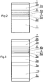
- Fig.1 , Fig.2 and Fig. 3 schematically show three embodiments of the laser structure according to the invention, while Fig.4 and Fig.5 show two optical characteristics of the laser diodes according to the invention.
- a GaO 0.0005 N 0 . 9995 substrate has been fabricated using the growth method from a nitride solution in gallium under the pressure of 1000 MPa and at temperature of 1500°C.
- the fabricated crystal has been cut and polished in order to obtain an optically flat platelet of typical thickness of 150-350 ⁇ m.
- the gallium site surface of the crystal after a proper mechanocemical polishing, featured atomic flatness, visible as atomic steps in the image of the Atomic Force Microscope.
- the crystal surface was disoriented by at least 0.5 deg. with respect to the crystallografic c axis of the hexagonal Wurzite structure.
- This substrate is marked in Fig.1 using reference number 1.
- the substrate 1 was placed in a MOVPE reactor, where a 600 nm thick Ga 0.2 Al 0.08 N layer 2a was grown at temperature about 1050°C and which was silicon-doped with the level of concentration reaching 5 x 10 18 cm -3 . Then, applying the same temperature growth, was fabricated an undoped GaN layer 3a of thickness about 100 nm and serving as the lower waveguide layer. After decreasing the temperature to 820°C the active region with multi quantum wells made of In 0.1 Ga 0.9 N/In 0.01 Ga 0.99 N, and number of repetition of the multi-quantum-well was three (layers 4a, 5, and 4b have been made three times).
- an 350 nm electron blocking layer 6 of Al 0.08 Ga 0.98 N was fabricated.
- upper waveguide layer 3b and upper cladding layer 2b were grown.
- the growth of the structure was terminated in a thin subcontact layer 7 of GaN:Mg with magnesium concentration larger than 10 20 cm -3 .
- the reactor chamber was cooled down in nitrogen ambient.
- the surfaces of the laser structure were patterned with metallic layers forming contacts to the n- and p- side of the crystal, in such a way that the upper contact was in a shape of a stripe of the length from 300 to 2000 ⁇ m and the width from 1 and 100 ⁇ m.
- Annealing of the contacts was performed under temperatures lower than 390°C.
- the laser can be etched with mesa, which then can be of 300-450 nm high, in order to improve lateral confinement of the electromagnetic mode.
- the threshold current density has been lowered by about 30% (see fig 4 , A - laser diode according to the invention, B-a known diode). Have been improved also near and far field patterns which indicate the mode leakage suppresion.
- a substrate 1 of GaO x N 1-x was fabricated and prepared in a way described in Example 1.
- the substrate 1 was placed in a MOVPE reactor, where at temperature about 1050°C an undoped 100 nm thick layer of GaN forming a lower waveguide layer 3a was fabricated.
- the active region with multi quantum wells of In 0.1 Ga 0.9 N/In 0.01 Ga 0.99 N was made, and the number of repetition of the multi-quantum-well was three (layers 4a, 5, and 4b were fabricated three times).
- the reactor temperature was risen to 1050°C and an electron blocking layer 6 of Al 0.12 Ga 0.88 N was fabricated.
- the upper waveguide 3b On the layer 6 an undoped GaN layer forming the upper waveguide 3b was grown.
- the next layer was the upper cladding layer 2b, which was made of 350 nm thick Al 0.08 Ga 0.98 N.
- the structure growth was terminated in a thin subcontact layer 7 of GaN:Mg with magnesium concentration larger than 10 20 cm -3 .
- the reactor chamber was cooled down in nitrogen ambient.
- the n- and p- side contacts were fabricated in the same way as described in Example 1. Also in this case the laser can be etched with mesa of 300-450 nm height, in order to improve lateral confinement of the electromagnetic mode.
- a silicon doped GaN crystal with the doping level of 5 x 10 18 cm -3 has been synthesized using HVPE method at temperature of 1050°C.
- the growth surface of this crystal was prepared in a way described in Example 1 and this substrate was marked in Fig.3 using reference number 1 b.
- the substrate 1 b was introduced into a high pressure reactor chamber, where using the growth method from a nitride solution in gallium under pressure of 1000 MPa and at temperature of 1500°C, on both sides of the HVPE seed GaO 0.005 N 0.995 layers were fabricated (layers 1a and 1c).
- the substrate 1 was placed in a MOVPE reactor, where a silicon-doped GaO 0.92 Al 008 N layer 2a of a thickness of 600 nm was grown at temperature 1050°C. Next, at the same temperature an undoped 100 nm thick GaN layer forming the bottom waveguide 3a was fabricated. After decreasing the temperature to 820°C the active region with multi quantum wells of In 0.1 Ga 0.9 N/In 0.01 Ga 0.99 N, and the number of repetition of the multi-quantum-well was three (layers 4a, 5, and 4b were fabricated three times).
- an electron blocking layer 6 of Al 0.12 Ga 0.88 N was fabricated, on which subsequently an undoped GaN layer forming the upper waveguide 3b was grown.
- the structure growth was terminated in a thin subcontact layer 7 of GaN:Mg with magnesium concentration larger than 10 20 cm -3 .
- the reactor chamber was cooled down in nitrogen ambient.
- the n- and p- side contacts were fabricated in the same way as described in Example 1. Also in this case the laser can be etched with mesa of 300-450 nm height, in order to improve lateral confinement of the electromagnetic mode.
- the threshold current density has been lowered by about 25% (see Fig.5 , A - a laser diode according to the invention, B - a known diode).
- the improved near and far field patterns indicate the mode leakage suppresion.
Landscapes
- Physics & Mathematics (AREA)
- Condensed Matter Physics & Semiconductors (AREA)
- General Physics & Mathematics (AREA)
- Electromagnetism (AREA)
- Optics & Photonics (AREA)
- Semiconductor Lasers (AREA)
Description
- The subject of this invention is a AlInGaN laser diode and a method of fabrication such laser diode.
- Present-day semiconductor laser diodes are usually fabricated as Separate Confinement Heterostructures, which means that the confinement for carriers and for the optical mode are determined separately by applying materials which differ in refractive index. A sequence of thin semiconductor films is deposited on a monocrystalline substrate, for example on GaAs, InP or GaN. A detail description of the method can be found, for example in: L. A. Coldren, S. W. Corzine, "Diode Lasers and Photonic Integrated Circuits" (Wiley Series in Microwave and Optical Engineering). The active region of such devices consist of quantum wells, bounded by quantum barriers. The electromagnetic mode propagates within the waveguide, which consists of high index layers enclosing the active region and which is then surrounded by low index layers. In the subsequent part of this description "laser waveguide" will be strictly referred to the transversal direction, which is the direction of the structure growth. The electromagnetic mode, or simply the mode will be referred to a specific spatial field distribution, which constitutes a solution to the wave equation in the waveguide. The lateral confinement can be obtained by any other means (index guiding, gain guiding, mesa, buried ridge) without loss of generality of the subsequently given reasoning/arguments. The electron blocking layer does not have to necessarily appear in all of the constructions. In case of lasers based on group III nitrides, emitting light within the spectral range between 400-500 nm, the above mentioned layers are realized using a specific method, which is described, among others, in: S. Nakamura, J. Mater. Res. 14, 2716 (1999) and in the patent publication
US 6,838,693 B2 . A 50 to 200 µm thick crystalline gallium nitride is used as a substrate. Cladding layers consist of aluminum-gallium nitride, AlxGa1-xN, for which x is from 0.05 to 0.12. The thickness of the cladding layers is from 0.5 to 5 µm. The bottom cladding layer is doped with silicon with doping level from 5 x 1019cm-3 to 1 x 1020cm-3. Waveguide layers usually consist of gallium nitride of thicknesses from 0.05 to 0.15 µm. The bottom waveguide can be silicon doped, and the upper waveguide can be magnesium doped. Both waveguide layers may also be undoped. The electron blocking layer is made of AlxGa1-xN, where x is from 0 to 0.3. The quantum well layer, in case of lasers emitting in the range of 400-500 nm is made of InxGa1-xN, where x ranging from 0 to 0.3 and its thickness ranges from 2 to 10 nm. The upper cladding layer is made of AlxGa1-xN, for which x is from 0.09 to 0.35 and its thickness is from 8 to 30 nm. In case of infrared lasers fabricated on a GaAs substrate, the waveguide is made of GaAs layers and AlGaAs cladding layers of high aluminum content. The high aluminum composition ensures the high refractive index contrast between the GaAs-core and the AlGaAs claddings. For example, laser emitting infrared radiation of the wavelength of around 900 nm that uses claddings with 50% aluminum content has the refractive index contrast of around 9% between the GaAs waveguide and AlGaAs claddings. The advantage of the GaAs-AlAs system is that the both compounds have closely matched lattice constants (the difference is only 0.2%). Due to this fact the whole structure can be strain-free. The situation is very different in case of gallium nitride structures. AlGaN, which serves for cladding layers, is lattice-mismatched to gallium nitride substrates (the lattice mismatch between GaN and AIN is of 2.5%). In consequence a strong tensile strain appears in AlGaN layers. If we go beyond a certain value of combination of the layer thickness and composition, a relaxation of strain occurs. This relaxation is realized through macroscopic cracking of the structure and/or generation of misfit dislocations. The maximal thickness and composition of AlGaN can be deduced from literature, for example from the paper: "Elimination of AlGaN epilayer cracking by spatially patterned AIN mask" by Marcin Sarzyński et al. Appl. Phys. Lett. 88, 121124 (2006), according to which obtaining a 40% AlGaN layer of thickness of 1 µm without cracking and other defects is not possible. Additional problem arising in nitride lasers, and which is a consequence of weak vertical confinement of the mode, is the mode leakage into the GaN substrate. Gallium nitride comprises both the waveguide core and the substrate and thus a strong tendency to the leaking of part of the mode into the substrate is observed, which at the same time significantly delimits the r factor describing the overlap between the optical mode and the active region. In order to avoid claddings, for example 2 µm thick with 5% AlGaN. From the paper Appl. Phys. Lett. 88, 121124 (2006) a conclusion can be made that such layer would not be cracked, however the amount of elastic energy accumulated in this layer must certainly lead to macroscopic bowing of the whole structure, which has detrimental influence on laser structure processing feasibility.US2008/0192788 A1 andUS2002/0109146A1 also disclose nitride semiconductor laser diodes. - An object of the invention was to fabricate a laser structure featuring better optoelectronic parameters, such as the threshold current and improved structure quality leading to better reliability of the device.
- The object is realized through a laser diode based on a AlInGaN alloy. The structure consists of the bottom cladding layer, which has a n-type conductivity, a bottom waveguide layer having also n-type conductivity, a light emitting (active) layer, an electron blocking layer of p-type conductivity, an upper waveguide layer and a subcontact layer, doped with acceptors with concentration level above 1020cm-3. In such diode the bottom cladding layer is made of GaOxN1-x alloy, where x>0.0005, a material of the bottom cladding layer has the refractive index at least one percent smaller (at wavelength of 405 nm) than the refractive index of a material comprising the upper and the bottom waveguide layer, and the bottom cladding layer thickness equals at least 10 µm.
- In one variant of the laser diode according to the invention the diode comprises first additional layer not thinner than 0.8 µm, which is made of AlyGa1-yN, where 0<y<0.1, and which is placed between the bottom cladding layer and the bottom waveguide layer.
- In another variant of the laser diode according to the invention the diode comprises two additional layers, the second and the third, which are placed below the bottom cladding layer. The second bottom cladding layer, made of 100 to 400 µm thick gallium nitride, is placed directly below the bottom cladding layer. The third additional layer, which is made of GaOxN1-x, where x > 0.0005, is placed directly below the second additional layer.
- In yet another variant of the laser diode according to the invention the second and the third additional layer have dislocation density lower than 1 x 107cm-2.
- A fabrication method of a laser diode based on AlInGaN alloy according to the invention relays on epitaxial growth of: a layer structure comprising at least the bottom cladding layer of n-type conductivity having at least one layer of GaOxN1-x, where x > 0.0005, a bottom waveguide layer of n-type conductivity, a light emitting layer, an electron blocking layer of p-type conductivity, an upper waveguide layer, an upper cladding layer of p-type conductivity and a subcontact layer doped with acceptors of concentration above 1020cm-3. At least one of the layers of the GaOxN1-x, is obtained using a high pressure method of nitride solution in gallium at pressures of 800 MPa. This method is characterized by that the bottom cladding layer is fabricated as a three layer structure. This structure contains two GaOxN1-x layers obtained from a nitride solution in gallium using the high pressure method at pressure above 800 MPa, which are grown on the inner gallium nitride layer of thickness of 100 to 400 µm.
- In a variant of the method according to the invention, in the fabricated three-layer structure of the bottom cladding layer, the upper GaOxN1-x layer has thickness from 2 to 100 µm.
- The invention entirely eliminates the mode leakage into the substrate, improving the optical confinement factor r and also improves the flatness of the surface leading to easier device processing and to a decrease of structural defects in a laser due to reduction of the lattice mismatch between the material of the lower waveguide cladding and the materials of other layers, including waveguide layers.
- The invention is presented in the accompanying drawings, where
Fig.1 ,Fig.2 and Fig. 3 schematically show three embodiments of the laser structure according to the invention, whileFig.4 and Fig.5 show two optical characteristics of the laser diodes according to the invention. - Below have been presented three laser diode structures according to the invention and method of their fabrication.
- In first step a GaO0.0005N0.9995 substrate has been fabricated using the growth method from a nitride solution in gallium under the pressure of 1000 MPa and at temperature of 1500°C. The fabricated crystal has been cut and polished in order to obtain an optically flat platelet of typical thickness of 150-350 µm. The gallium site surface of the crystal, after a proper mechanocemical polishing, featured atomic flatness, visible as atomic steps in the image of the Atomic Force Microscope. The crystal surface was disoriented by at least 0.5 deg. with respect to the crystallografic c axis of the hexagonal Wurzite structure. This substrate is marked in
Fig.1 usingreference number 1. Next, thesubstrate 1 was placed in a MOVPE reactor, where a 600 nm thick Ga0.2Al0.08N layer 2a was grown at temperature about 1050°C and which was silicon-doped with the level of concentration reaching 5 x 1018cm-3. Then, applying the same temperature growth, was fabricated anundoped GaN layer 3a of thickness about 100 nm and serving as the lower waveguide layer. After decreasing the temperature to 820°C the active region with multi quantum wells made of In0.1Ga0.9N/In0.01Ga0.99N, and number of repetition of the multi-quantum-well was three (layers electron blocking layer 6 of Al0.08Ga0.98N was fabricated. As next layers of the laser structureupper waveguide layer 3b andupper cladding layer 2b were grown. The growth of the structure was terminated in athin subcontact layer 7 of GaN:Mg with magnesium concentration larger than 1020cm-3. After termination the growth process, the reactor chamber was cooled down in nitrogen ambient. Next, the surfaces of the laser structure were patterned with metallic layers forming contacts to the n- and p- side of the crystal, in such a way that the upper contact was in a shape of a stripe of the length from 300 to 2000 µm and the width from 1 and 100 µm. Annealing of the contacts was performed under temperatures lower than 390°C. The laser can be etched with mesa, which then can be of 300-450 nm high, in order to improve lateral confinement of the electromagnetic mode. Using the GaOxN1-x substrate, the threshold current density has been lowered by about 30% (seefig 4 , A - laser diode according to the invention, B-a known diode). Have been improved also near and far field patterns which indicate the mode leakage suppresion. - In the first step a
substrate 1 of GaOxN1-x was fabricated and prepared in a way described in Example 1. Next, thesubstrate 1 was placed in a MOVPE reactor, where at temperature about 1050°C an undoped 100 nm thick layer of GaN forming alower waveguide layer 3a was fabricated. After decreasing the temperature to 820°C the active region with multi quantum wells of In0.1Ga0.9N/In0.01Ga0.99N was made, and the number of repetition of the multi-quantum-well was three (layers electron blocking layer 6 of Al0.12Ga0.88N was fabricated. On thelayer 6 an undoped GaN layer forming theupper waveguide 3b was grown. The next layer was theupper cladding layer 2b, which was made of 350 nm thick Al0.08Ga0.98N. The structure growth was terminated in athin subcontact layer 7 of GaN:Mg with magnesium concentration larger than 1020cm-3. After termination the growth process, the reactor chamber was cooled down in nitrogen ambient. The n- and p- side contacts were fabricated in the same way as described in Example 1. Also in this case the laser can be etched with mesa of 300-450 nm height, in order to improve lateral confinement of the electromagnetic mode. - In the first step of the laser diode structure fabrication, a silicon doped GaN crystal with the doping level of 5 x 1018cm-3 has been synthesized using HVPE method at temperature of 1050°C. The growth surface of this crystal was prepared in a way described in Example 1 and this substrate was marked in
Fig.3 usingreference number 1 b. Thesubstrate 1 b was introduced into a high pressure reactor chamber, where using the growth method from a nitride solution in gallium under pressure of 1000 MPa and at temperature of 1500°C, on both sides of the HVPE seed GaO0.005N0.995 layers were fabricated (layers layers substrate 1 was placed in a MOVPE reactor, where a silicon-doped GaO0.92Al008N layer 2a of a thickness of 600 nm was grown at temperature 1050°C. Next, at the same temperature an undoped 100 nm thick GaN layer forming thebottom waveguide 3a was fabricated. After decreasing the temperature to 820°C the active region with multi quantum wells of In0.1Ga0.9N/In0.01Ga0.99N, and the number of repetition of the multi-quantum-well was three (layers electron blocking layer 6 of Al0.12Ga0.88N was fabricated, on which subsequently an undoped GaN layer forming theupper waveguide 3b was grown. Next layer was anupper cladding layer 2b, which was made of 350 nm thick Al0.08Ga0.98N. The structure growth was terminated in athin subcontact layer 7 of GaN:Mg with magnesium concentration larger than 1020cm-3. After termination the growth process, the reactor chamber was cooled down in nitrogen ambient. The n- and p- side contacts were fabricated in the same way as described in Example 1. Also in this case the laser can be etched with mesa of 300-450 nm height, in order to improve lateral confinement of the electromagnetic mode. Using the GaOxN1-x substrate, the threshold current density has been lowered by about 25% (seeFig.5 , A - a laser diode according to the invention, B - a known diode). The improved near and far field patterns indicate the mode leakage suppresion.
Claims (6)
- A laser diode based on AlInGaN alloy, comprising a bottom cladding layer (1) of n-type conductivity made of GaOxN1-x alloy, in which x>0.0005, a bottom waveguide layer (3a) of n-type conductivity, a light emitting layer (4a,5,46), an electron blocking layer (6) of p-type conductivity, an upper waveguide layer (3b) of p-type conductivity, an upper cladding layer (2b) of p-type conductivity and a subcontact layer (7), doped with acceptors with concentration level above 1020cm-3, characterized in that thickness of the bottom cladding layer (1) is at least 10 µm and a material of the bottom cladding layer (1) possess the refractive index at least one percent lower (at the wavelength of 405 nm) than the refractive index of a material constituting the bottom waveguide layer (3a) and the upper (3b) waveguide layer.
- The laser diode according to one of Claim 1, characterized in that it comprises a first additional layer (2a) of thickness not smaller than 0.8 µm, made of AlyGa1-yN alloy for which 0<y<1, and situated between the bottom cladding layer (1) and the bottom waveguide layer (3a).
- The laser diode according to Claim 1 or 2, characterized in that it comprises two additional layers, the second (1a) and the third (1c), situated below the bottom cladding layer (1), and in that directly under the bottom cladding layer (1) the second additional layer (1 a) of a gallium nitride seed of the thickness of 100 to 400 µm is located while directly underneath there is the third additional layer (1c) of 2 to 100 µm thick GaOxN1-x in which x>0.0005.
- The laser diode according to Claim 3, characterized in that the second additional layer (1a) and the third additional layer (1c) have dislocation densities lower than 1 x 107cm-2.
- A method of fabricating a laser diode based on AlInGaN alloy, consisting in epitaxial growth of a layer structure consisting of at least one bottom cladding layer of n-type conductivity comprising at least one GaOxN1-x layer (1, 1a, 1c) in which x>0.0005, a bottom waveguide layer of n-type conductivity, a light emitting layer, an electron blocking layer of p-type conductivity and an acceptor-doped subcontact layer with concentrations above 1020cm-3, in which at least one layer is grown using a high pressure method of nitride solution in gallium at pressures of 800 MPa, characterized in that the bottom cladding layer (1a, 1b, 1c) is fabricated as three layer structure comprising two layers (1a, 1c) of GaOxN1-x deposited on the middle (inner) layer (1b) of gallium nitride of thickness of 100 to 400 µm, using the high pressure method of nitride solution in gallium at pressures of 800 MPa.
- The method according to Claim 5, characterized in that the fabricated three layer structure of the bottom cladding layer (1a, 1b, 1c) the upper layer (1a), made of GaOxN1-x is at least 10 µm thick, and the bottom layer (1c), made of GaOxN1-x is of 2 to 100 µm thick.
Applications Claiming Priority (2)
| Application Number | Priority Date | Filing Date | Title |
|---|---|---|---|
| PL388149A PL217437B1 (en) | 2009-05-30 | 2009-05-30 | Laser diode and method for production thereof |
| PCT/PL2010/050018 WO2010140909A1 (en) | 2009-05-30 | 2010-05-22 | Laser diode and method of fabrication the laser diode |
Publications (2)
| Publication Number | Publication Date |
|---|---|
| EP2438663A1 EP2438663A1 (en) | 2012-04-11 |
| EP2438663B1 true EP2438663B1 (en) | 2014-12-31 |
Family
ID=42872444
Family Applications (1)
| Application Number | Title | Priority Date | Filing Date |
|---|---|---|---|
| EP10728441.6A Not-in-force EP2438663B1 (en) | 2009-05-30 | 2010-05-22 | Laser diode and method of fabrication the laser diode |
Country Status (4)
| Country | Link |
|---|---|
| US (1) | US20120147915A1 (en) |
| EP (1) | EP2438663B1 (en) |
| PL (1) | PL217437B1 (en) |
| WO (1) | WO2010140909A1 (en) |
Families Citing this family (3)
| Publication number | Priority date | Publication date | Assignee | Title |
|---|---|---|---|---|
| DE102010043693A1 (en) * | 2010-09-29 | 2012-03-29 | Robert Bosch Gmbh | A semiconductor laser device and method of manufacturing a semiconductor laser device |
| CN114825048B (en) * | 2022-04-08 | 2025-03-14 | 安徽格恩半导体有限公司 | A semiconductor laser element |
| CN114825049B (en) * | 2022-04-20 | 2025-03-14 | 安徽格恩半导体有限公司 | A semiconductor laser |
Family Cites Families (4)
| Publication number | Priority date | Publication date | Assignee | Title |
|---|---|---|---|---|
| US6586762B2 (en) | 2000-07-07 | 2003-07-01 | Nichia Corporation | Nitride semiconductor device with improved lifetime and high output power |
| JP3639789B2 (en) * | 2001-01-31 | 2005-04-20 | シャープ株式会社 | Nitride semiconductor light emitting device |
| JP2004014938A (en) * | 2002-06-10 | 2004-01-15 | Matsushita Electric Ind Co Ltd | Semiconductor device and manufacturing method thereof |
| US7408199B2 (en) * | 2004-04-02 | 2008-08-05 | Nichia Corporation | Nitride semiconductor laser device and nitride semiconductor device |
-
2009
- 2009-05-30 PL PL388149A patent/PL217437B1/en unknown
-
2010
- 2010-05-22 EP EP10728441.6A patent/EP2438663B1/en not_active Not-in-force
- 2010-05-22 US US13/261,057 patent/US20120147915A1/en not_active Abandoned
- 2010-05-22 WO PCT/PL2010/050018 patent/WO2010140909A1/en not_active Ceased
Also Published As
| Publication number | Publication date |
|---|---|
| PL217437B1 (en) | 2014-07-31 |
| EP2438663A1 (en) | 2012-04-11 |
| PL388149A1 (en) | 2010-12-06 |
| WO2010140909A1 (en) | 2010-12-09 |
| US20120147915A1 (en) | 2012-06-14 |
Similar Documents
| Publication | Publication Date | Title |
|---|---|---|
| EP1184913B1 (en) | Nitride semiconductor laser diode | |
| US8410523B2 (en) | Misfit dislocation forming interfacial self-assembly for growth of highly-mismatched III-SB alloys | |
| JP4173445B2 (en) | Nitride semiconductor substrate, method for manufacturing the same, and semiconductor light emitting device using the same | |
| US11201261B2 (en) | Deep ultraviolet light emitting element and method of manufacturing the same | |
| US20010032975A1 (en) | Nitride based semiconductor photo-luminescent device | |
| KR100705886B1 (en) | Nitride semiconductor layer structure and nitride semiconductor laser | |
| Shang et al. | Low-threshold epitaxially grown 1.3-μm InAs quantum dot lasers on patterned (001) Si | |
| JP2004111766A (en) | Gallium nitride based semiconductor device and method of manufacturing the same | |
| US20070160100A1 (en) | Misfit dislocation forming interfacial self-assembly for growth of highly-mismatched III-Sb alloys | |
| JP6248148B2 (en) | Optoelectronic semiconductor body and method of manufacturing optoelectronic semiconductor body | |
| US8268659B2 (en) | Edge-emitting semiconductor laser chip | |
| CN115548877A (en) | Laser radar-oriented 1550nm waveband high-power semiconductor laser epitaxial structure and method | |
| US7588954B2 (en) | InGaAs/GaAs lasers on silicon produced by LEPECVD and MOCVD | |
| US9099842B2 (en) | Laser emission systems, heterostructure and active zone having coupled quantum-wells, and use for 1.55 mm laser emission | |
| US20120147915A1 (en) | Laser diode and method of fabrication the laser diode | |
| EP3375056B1 (en) | Alingan alloy based laser diode | |
| Tang et al. | Investigation into the InAs/GaAs quantum dot material epitaxially grown on silicon for O band lasers | |
| EP0945939A2 (en) | Semiconductor light-emitting device | |
| US8895335B1 (en) | Impurity-induced disorder in III-nitride materials and devices | |
| KR20040093671A (en) | Vertical Cavity Surface Emitting Laser Including Indium In The Active Region | |
| EP4049083B1 (en) | Semiconductor structure and fabrication of a semiconductor structure with multiple quantum wells | |
| KR20100063058A (en) | Compound semiconductor epitaxial wafer and process for producing the same | |
| Jia et al. | InAs/InAlGaAs quantum dot lasers on InP and Si | |
| Perlin et al. | Plasmonic cladding InGaN MQW laser diodes | |
| JP2005191499A (en) | Compound semiconductor, compound semiconductor crystal, and semiconductor device and semiconductor laser using the compound semiconductor and compound semiconductor crystal |
Legal Events
| Date | Code | Title | Description |
|---|---|---|---|
| PUAI | Public reference made under article 153(3) epc to a published international application that has entered the european phase |
Free format text: ORIGINAL CODE: 0009012 |
|
| 17P | Request for examination filed |
Effective date: 20111227 |
|
| AK | Designated contracting states |
Kind code of ref document: A1 Designated state(s): AL AT BE BG CH CY CZ DE DK EE ES FI FR GB GR HR HU IE IS IT LI LT LU LV MC MK MT NL NO PL PT RO SE SI SK SM TR |
|
| DAX | Request for extension of the european patent (deleted) | ||
| GRAP | Despatch of communication of intention to grant a patent |
Free format text: ORIGINAL CODE: EPIDOSNIGR1 |
|
| INTG | Intention to grant announced |
Effective date: 20140718 |
|
| GRAS | Grant fee paid |
Free format text: ORIGINAL CODE: EPIDOSNIGR3 |
|
| GRAA | (expected) grant |
Free format text: ORIGINAL CODE: 0009210 |
|
| AK | Designated contracting states |
Kind code of ref document: B1 Designated state(s): AL AT BE BG CH CY CZ DE DK EE ES FI FR GB GR HR HU IE IS IT LI LT LU LV MC MK MT NL NO PL PT RO SE SI SK SM TR |
|
| REG | Reference to a national code |
Ref country code: CH Ref legal event code: EP Ref country code: GB Ref legal event code: FG4D |
|
| REG | Reference to a national code |
Ref country code: IE Ref legal event code: FG4D |
|
| REG | Reference to a national code |
Ref country code: AT Ref legal event code: REF Ref document number: 704882 Country of ref document: AT Kind code of ref document: T Effective date: 20150215 |
|
| REG | Reference to a national code |
Ref country code: DE Ref legal event code: R096 Ref document number: 602010021425 Country of ref document: DE Effective date: 20150219 |
|
| PG25 | Lapsed in a contracting state [announced via postgrant information from national office to epo] |
Ref country code: NO Free format text: LAPSE BECAUSE OF FAILURE TO SUBMIT A TRANSLATION OF THE DESCRIPTION OR TO PAY THE FEE WITHIN THE PRESCRIBED TIME-LIMIT Effective date: 20150331 Ref country code: FI Free format text: LAPSE BECAUSE OF FAILURE TO SUBMIT A TRANSLATION OF THE DESCRIPTION OR TO PAY THE FEE WITHIN THE PRESCRIBED TIME-LIMIT Effective date: 20141231 Ref country code: LT Free format text: LAPSE BECAUSE OF FAILURE TO SUBMIT A TRANSLATION OF THE DESCRIPTION OR TO PAY THE FEE WITHIN THE PRESCRIBED TIME-LIMIT Effective date: 20141231 |
|
| REG | Reference to a national code |
Ref country code: NL Ref legal event code: VDEP Effective date: 20141231 |
|
| REG | Reference to a national code |
Ref country code: LT Ref legal event code: MG4D |
|
| PG25 | Lapsed in a contracting state [announced via postgrant information from national office to epo] |
Ref country code: LV Free format text: LAPSE BECAUSE OF FAILURE TO SUBMIT A TRANSLATION OF THE DESCRIPTION OR TO PAY THE FEE WITHIN THE PRESCRIBED TIME-LIMIT Effective date: 20141231 Ref country code: HR Free format text: LAPSE BECAUSE OF FAILURE TO SUBMIT A TRANSLATION OF THE DESCRIPTION OR TO PAY THE FEE WITHIN THE PRESCRIBED TIME-LIMIT Effective date: 20141231 Ref country code: GR Free format text: LAPSE BECAUSE OF FAILURE TO SUBMIT A TRANSLATION OF THE DESCRIPTION OR TO PAY THE FEE WITHIN THE PRESCRIBED TIME-LIMIT Effective date: 20150401 Ref country code: SE Free format text: LAPSE BECAUSE OF FAILURE TO SUBMIT A TRANSLATION OF THE DESCRIPTION OR TO PAY THE FEE WITHIN THE PRESCRIBED TIME-LIMIT Effective date: 20141231 |
|
| REG | Reference to a national code |
Ref country code: AT Ref legal event code: MK05 Ref document number: 704882 Country of ref document: AT Kind code of ref document: T Effective date: 20141231 |
|
| PG25 | Lapsed in a contracting state [announced via postgrant information from national office to epo] |
Ref country code: NL Free format text: LAPSE BECAUSE OF FAILURE TO SUBMIT A TRANSLATION OF THE DESCRIPTION OR TO PAY THE FEE WITHIN THE PRESCRIBED TIME-LIMIT Effective date: 20141231 |
|
| PG25 | Lapsed in a contracting state [announced via postgrant information from national office to epo] |
Ref country code: SK Free format text: LAPSE BECAUSE OF FAILURE TO SUBMIT A TRANSLATION OF THE DESCRIPTION OR TO PAY THE FEE WITHIN THE PRESCRIBED TIME-LIMIT Effective date: 20141231 Ref country code: CZ Free format text: LAPSE BECAUSE OF FAILURE TO SUBMIT A TRANSLATION OF THE DESCRIPTION OR TO PAY THE FEE WITHIN THE PRESCRIBED TIME-LIMIT Effective date: 20141231 Ref country code: RO Free format text: LAPSE BECAUSE OF FAILURE TO SUBMIT A TRANSLATION OF THE DESCRIPTION OR TO PAY THE FEE WITHIN THE PRESCRIBED TIME-LIMIT Effective date: 20141231 Ref country code: ES Free format text: LAPSE BECAUSE OF FAILURE TO SUBMIT A TRANSLATION OF THE DESCRIPTION OR TO PAY THE FEE WITHIN THE PRESCRIBED TIME-LIMIT Effective date: 20141231 |
|
| PG25 | Lapsed in a contracting state [announced via postgrant information from national office to epo] |
Ref country code: IS Free format text: LAPSE BECAUSE OF FAILURE TO SUBMIT A TRANSLATION OF THE DESCRIPTION OR TO PAY THE FEE WITHIN THE PRESCRIBED TIME-LIMIT Effective date: 20150430 Ref country code: AT Free format text: LAPSE BECAUSE OF FAILURE TO SUBMIT A TRANSLATION OF THE DESCRIPTION OR TO PAY THE FEE WITHIN THE PRESCRIBED TIME-LIMIT Effective date: 20141231 Ref country code: PL Free format text: LAPSE BECAUSE OF FAILURE TO SUBMIT A TRANSLATION OF THE DESCRIPTION OR TO PAY THE FEE WITHIN THE PRESCRIBED TIME-LIMIT Effective date: 20141231 |
|
| REG | Reference to a national code |
Ref country code: DE Ref legal event code: R097 Ref document number: 602010021425 Country of ref document: DE |
|
| PG25 | Lapsed in a contracting state [announced via postgrant information from national office to epo] |
Ref country code: DK Free format text: LAPSE BECAUSE OF FAILURE TO SUBMIT A TRANSLATION OF THE DESCRIPTION OR TO PAY THE FEE WITHIN THE PRESCRIBED TIME-LIMIT Effective date: 20141231 Ref country code: EE Free format text: LAPSE BECAUSE OF FAILURE TO SUBMIT A TRANSLATION OF THE DESCRIPTION OR TO PAY THE FEE WITHIN THE PRESCRIBED TIME-LIMIT Effective date: 20141231 |
|
| PLBE | No opposition filed within time limit |
Free format text: ORIGINAL CODE: 0009261 |
|
| STAA | Information on the status of an ep patent application or granted ep patent |
Free format text: STATUS: NO OPPOSITION FILED WITHIN TIME LIMIT |
|
| 26N | No opposition filed |
Effective date: 20151001 |
|
| PG25 | Lapsed in a contracting state [announced via postgrant information from national office to epo] |
Ref country code: IT Free format text: LAPSE BECAUSE OF FAILURE TO SUBMIT A TRANSLATION OF THE DESCRIPTION OR TO PAY THE FEE WITHIN THE PRESCRIBED TIME-LIMIT Effective date: 20141231 |
|
| REG | Reference to a national code |
Ref country code: CH Ref legal event code: PL |
|
| PG25 | Lapsed in a contracting state [announced via postgrant information from national office to epo] |
Ref country code: CH Free format text: LAPSE BECAUSE OF NON-PAYMENT OF DUE FEES Effective date: 20150531 Ref country code: LU Free format text: LAPSE BECAUSE OF FAILURE TO SUBMIT A TRANSLATION OF THE DESCRIPTION OR TO PAY THE FEE WITHIN THE PRESCRIBED TIME-LIMIT Effective date: 20150522 Ref country code: LI Free format text: LAPSE BECAUSE OF NON-PAYMENT OF DUE FEES Effective date: 20150531 Ref country code: MC Free format text: LAPSE BECAUSE OF FAILURE TO SUBMIT A TRANSLATION OF THE DESCRIPTION OR TO PAY THE FEE WITHIN THE PRESCRIBED TIME-LIMIT Effective date: 20141231 |
|
| REG | Reference to a national code |
Ref country code: IE Ref legal event code: MM4A |
|
| PG25 | Lapsed in a contracting state [announced via postgrant information from national office to epo] |
Ref country code: SI Free format text: LAPSE BECAUSE OF FAILURE TO SUBMIT A TRANSLATION OF THE DESCRIPTION OR TO PAY THE FEE WITHIN THE PRESCRIBED TIME-LIMIT Effective date: 20141231 |
|
| PG25 | Lapsed in a contracting state [announced via postgrant information from national office to epo] |
Ref country code: IE Free format text: LAPSE BECAUSE OF NON-PAYMENT OF DUE FEES Effective date: 20150522 |
|
| REG | Reference to a national code |
Ref country code: FR Ref legal event code: PLFP Year of fee payment: 7 |
|
| PG25 | Lapsed in a contracting state [announced via postgrant information from national office to epo] |
Ref country code: BE Free format text: LAPSE BECAUSE OF FAILURE TO SUBMIT A TRANSLATION OF THE DESCRIPTION OR TO PAY THE FEE WITHIN THE PRESCRIBED TIME-LIMIT Effective date: 20141231 |
|
| PG25 | Lapsed in a contracting state [announced via postgrant information from national office to epo] |
Ref country code: MT Free format text: LAPSE BECAUSE OF FAILURE TO SUBMIT A TRANSLATION OF THE DESCRIPTION OR TO PAY THE FEE WITHIN THE PRESCRIBED TIME-LIMIT Effective date: 20141231 |
|
| REG | Reference to a national code |
Ref country code: FR Ref legal event code: PLFP Year of fee payment: 8 |
|
| PG25 | Lapsed in a contracting state [announced via postgrant information from national office to epo] |
Ref country code: HU Free format text: LAPSE BECAUSE OF FAILURE TO SUBMIT A TRANSLATION OF THE DESCRIPTION OR TO PAY THE FEE WITHIN THE PRESCRIBED TIME-LIMIT; INVALID AB INITIO Effective date: 20100522 Ref country code: SM Free format text: LAPSE BECAUSE OF FAILURE TO SUBMIT A TRANSLATION OF THE DESCRIPTION OR TO PAY THE FEE WITHIN THE PRESCRIBED TIME-LIMIT Effective date: 20141231 Ref country code: BG Free format text: LAPSE BECAUSE OF FAILURE TO SUBMIT A TRANSLATION OF THE DESCRIPTION OR TO PAY THE FEE WITHIN THE PRESCRIBED TIME-LIMIT Effective date: 20141231 |
|
| PG25 | Lapsed in a contracting state [announced via postgrant information from national office to epo] |
Ref country code: CY Free format text: LAPSE BECAUSE OF FAILURE TO SUBMIT A TRANSLATION OF THE DESCRIPTION OR TO PAY THE FEE WITHIN THE PRESCRIBED TIME-LIMIT Effective date: 20141231 |
|
| PG25 | Lapsed in a contracting state [announced via postgrant information from national office to epo] |
Ref country code: TR Free format text: LAPSE BECAUSE OF FAILURE TO SUBMIT A TRANSLATION OF THE DESCRIPTION OR TO PAY THE FEE WITHIN THE PRESCRIBED TIME-LIMIT Effective date: 20141231 |
|
| REG | Reference to a national code |
Ref country code: FR Ref legal event code: PLFP Year of fee payment: 9 |
|
| PG25 | Lapsed in a contracting state [announced via postgrant information from national office to epo] |
Ref country code: MK Free format text: LAPSE BECAUSE OF FAILURE TO SUBMIT A TRANSLATION OF THE DESCRIPTION OR TO PAY THE FEE WITHIN THE PRESCRIBED TIME-LIMIT Effective date: 20141231 |
|
| PG25 | Lapsed in a contracting state [announced via postgrant information from national office to epo] |
Ref country code: PT Free format text: LAPSE BECAUSE OF FAILURE TO SUBMIT A TRANSLATION OF THE DESCRIPTION OR TO PAY THE FEE WITHIN THE PRESCRIBED TIME-LIMIT Effective date: 20141231 |
|
| PG25 | Lapsed in a contracting state [announced via postgrant information from national office to epo] |
Ref country code: AL Free format text: LAPSE BECAUSE OF FAILURE TO SUBMIT A TRANSLATION OF THE DESCRIPTION OR TO PAY THE FEE WITHIN THE PRESCRIBED TIME-LIMIT Effective date: 20141231 |
|
| PGFP | Annual fee paid to national office [announced via postgrant information from national office to epo] |
Ref country code: GB Payment date: 20220630 Year of fee payment: 13 |
|
| PGFP | Annual fee paid to national office [announced via postgrant information from national office to epo] |
Ref country code: FR Payment date: 20220813 Year of fee payment: 13 |
|
| PGFP | Annual fee paid to national office [announced via postgrant information from national office to epo] |
Ref country code: DE Payment date: 20221117 Year of fee payment: 13 |
|
| REG | Reference to a national code |
Ref country code: DE Ref legal event code: R119 Ref document number: 602010021425 Country of ref document: DE |
|
| GBPC | Gb: european patent ceased through non-payment of renewal fee |
Effective date: 20230522 |
|
| PG25 | Lapsed in a contracting state [announced via postgrant information from national office to epo] |
Ref country code: DE Free format text: LAPSE BECAUSE OF NON-PAYMENT OF DUE FEES Effective date: 20231201 Ref country code: GB Free format text: LAPSE BECAUSE OF NON-PAYMENT OF DUE FEES Effective date: 20230522 |
|
| PG25 | Lapsed in a contracting state [announced via postgrant information from national office to epo] |
Ref country code: FR Free format text: LAPSE BECAUSE OF NON-PAYMENT OF DUE FEES Effective date: 20230531 |