EP2434318A2 - Production method of optical waveguide for connector - Google Patents
Production method of optical waveguide for connector Download PDFInfo
- Publication number
- EP2434318A2 EP2434318A2 EP11182149A EP11182149A EP2434318A2 EP 2434318 A2 EP2434318 A2 EP 2434318A2 EP 11182149 A EP11182149 A EP 11182149A EP 11182149 A EP11182149 A EP 11182149A EP 2434318 A2 EP2434318 A2 EP 2434318A2
- Authority
- EP
- European Patent Office
- Prior art keywords
- cladding layer
- optical waveguide
- cores
- core
- over
- Prior art date
- Legal status (The legal status is an assumption and is not a legal conclusion. Google has not performed a legal analysis and makes no representation as to the accuracy of the status listed.)
- Withdrawn
Links
- 230000003287 optical effect Effects 0.000 title claims abstract description 131
- 238000004519 manufacturing process Methods 0.000 title claims abstract description 28
- 238000005253 cladding Methods 0.000 claims abstract description 114
- 229920005989 resin Polymers 0.000 claims abstract description 47
- 239000011347 resin Substances 0.000 claims abstract description 47
- 230000015572 biosynthetic process Effects 0.000 claims abstract description 43
- 238000010438 heat treatment Methods 0.000 claims abstract description 36
- 239000011162 core material Substances 0.000 claims description 167
- 239000000463 material Substances 0.000 claims description 34
- 239000000758 substrate Substances 0.000 claims description 29
- 230000005855 radiation Effects 0.000 claims description 25
- 239000000203 mixture Substances 0.000 claims description 8
- 230000008878 coupling Effects 0.000 abstract description 8
- 238000010168 coupling process Methods 0.000 abstract description 8
- 238000005859 coupling reaction Methods 0.000 abstract description 8
- 239000010410 layer Substances 0.000 description 212
- 230000000052 comparative effect Effects 0.000 description 55
- 239000011342 resin composition Substances 0.000 description 30
- 230000005540 biological transmission Effects 0.000 description 19
- 238000005259 measurement Methods 0.000 description 15
- 238000009826 distribution Methods 0.000 description 12
- 239000002904 solvent Substances 0.000 description 12
- 229920003207 poly(ethylene-2,6-naphthalate) Polymers 0.000 description 11
- 229920000139 polyethylene terephthalate Polymers 0.000 description 11
- 239000003822 epoxy resin Substances 0.000 description 9
- 238000011156 evaluation Methods 0.000 description 9
- 239000011521 glass Substances 0.000 description 9
- 238000000034 method Methods 0.000 description 9
- 229920000647 polyepoxide Polymers 0.000 description 9
- 229910001220 stainless steel Inorganic materials 0.000 description 9
- 239000010935 stainless steel Substances 0.000 description 9
- 238000003756 stirring Methods 0.000 description 7
- 239000000126 substance Substances 0.000 description 7
- LZCLXQDLBQLTDK-UHFFFAOYSA-N ethyl 2-hydroxypropanoate Chemical compound CCOC(=O)C(C)O LZCLXQDLBQLTDK-UHFFFAOYSA-N 0.000 description 6
- 230000001186 cumulative effect Effects 0.000 description 5
- QSHDDOUJBYECFT-UHFFFAOYSA-N mercury Chemical compound [Hg] QSHDDOUJBYECFT-UHFFFAOYSA-N 0.000 description 5
- 229910052753 mercury Inorganic materials 0.000 description 5
- 239000011247 coating layer Substances 0.000 description 4
- 238000010586 diagram Methods 0.000 description 4
- 230000010365 information processing Effects 0.000 description 4
- -1 polyethylene terephthalates Polymers 0.000 description 4
- 229920001187 thermosetting polymer Polymers 0.000 description 4
- 125000002723 alicyclic group Chemical group 0.000 description 3
- 229940116333 ethyl lactate Drugs 0.000 description 3
- 239000000835 fiber Substances 0.000 description 3
- 230000006870 function Effects 0.000 description 3
- 239000003960 organic solvent Substances 0.000 description 3
- 238000000206 photolithography Methods 0.000 description 3
- 239000007787 solid Substances 0.000 description 3
- YEJRWHAVMIAJKC-UHFFFAOYSA-N 4-Butyrolactone Chemical compound O=C1CCCO1 YEJRWHAVMIAJKC-UHFFFAOYSA-N 0.000 description 2
- 241001050985 Disco Species 0.000 description 2
- DXXIFYGOFNDTND-UHFFFAOYSA-N carbonic acid;pentan-3-one Chemical compound OC(O)=O.CCC(=O)CC DXXIFYGOFNDTND-UHFFFAOYSA-N 0.000 description 2
- 239000011248 coating agent Substances 0.000 description 2
- 238000000576 coating method Methods 0.000 description 2
- JHIVVAPYMSGYDF-UHFFFAOYSA-N cyclohexanone Chemical compound O=C1CCCCC1 JHIVVAPYMSGYDF-UHFFFAOYSA-N 0.000 description 2
- 230000003247 decreasing effect Effects 0.000 description 2
- 238000011161 development Methods 0.000 description 2
- 238000007598 dipping method Methods 0.000 description 2
- 230000015654 memory Effects 0.000 description 2
- QWVGKYWNOKOFNN-UHFFFAOYSA-N o-cresol Chemical compound CC1=CC=CC=C1O QWVGKYWNOKOFNN-UHFFFAOYSA-N 0.000 description 2
- 125000003566 oxetanyl group Chemical group 0.000 description 2
- 125000005409 triarylsulfonium group Chemical group 0.000 description 2
- 125000003118 aryl group Chemical group 0.000 description 1
- 238000010276 construction Methods 0.000 description 1
- 239000013256 coordination polymer Substances 0.000 description 1
- 238000005520 cutting process Methods 0.000 description 1
- 229910003460 diamond Inorganic materials 0.000 description 1
- GYZLOYUZLJXAJU-UHFFFAOYSA-N diglycidyl ether Chemical compound C1OC1COCC1CO1 GYZLOYUZLJXAJU-UHFFFAOYSA-N 0.000 description 1
- 230000000694 effects Effects 0.000 description 1
- 230000005284 excitation Effects 0.000 description 1
- 239000011888 foil Substances 0.000 description 1
- 230000010354 integration Effects 0.000 description 1
- 239000007788 liquid Substances 0.000 description 1
- 239000004850 liquid epoxy resins (LERs) Substances 0.000 description 1
- 229910052751 metal Inorganic materials 0.000 description 1
- 239000002184 metal Substances 0.000 description 1
- 150000002739 metals Chemical class 0.000 description 1
- 238000012986 modification Methods 0.000 description 1
- 230000004048 modification Effects 0.000 description 1
- 229920003986 novolac Polymers 0.000 description 1
- 239000010453 quartz Substances 0.000 description 1
- 229910052710 silicon Inorganic materials 0.000 description 1
- 239000010703 silicon Substances 0.000 description 1
- VYPSYNLAJGMNEJ-UHFFFAOYSA-N silicon dioxide Inorganic materials O=[Si]=O VYPSYNLAJGMNEJ-UHFFFAOYSA-N 0.000 description 1
- 230000008961 swelling Effects 0.000 description 1
- 238000009966 trimming Methods 0.000 description 1
Images





Classifications
-
- G—PHYSICS
- G02—OPTICS
- G02B—OPTICAL ELEMENTS, SYSTEMS OR APPARATUS
- G02B6/00—Light guides; Structural details of arrangements comprising light guides and other optical elements, e.g. couplings
- G02B6/10—Light guides; Structural details of arrangements comprising light guides and other optical elements, e.g. couplings of the optical waveguide type
- G02B6/12—Light guides; Structural details of arrangements comprising light guides and other optical elements, e.g. couplings of the optical waveguide type of the integrated circuit kind
- G02B6/122—Basic optical elements, e.g. light-guiding paths
-
- G—PHYSICS
- G02—OPTICS
- G02B—OPTICAL ELEMENTS, SYSTEMS OR APPARATUS
- G02B6/00—Light guides; Structural details of arrangements comprising light guides and other optical elements, e.g. couplings
- G02B6/10—Light guides; Structural details of arrangements comprising light guides and other optical elements, e.g. couplings of the optical waveguide type
- G02B6/12—Light guides; Structural details of arrangements comprising light guides and other optical elements, e.g. couplings of the optical waveguide type of the integrated circuit kind
- G02B6/13—Integrated optical circuits characterised by the manufacturing method
- G02B6/138—Integrated optical circuits characterised by the manufacturing method by using polymerisation
-
- G—PHYSICS
- G02—OPTICS
- G02B—OPTICAL ELEMENTS, SYSTEMS OR APPARATUS
- G02B6/00—Light guides; Structural details of arrangements comprising light guides and other optical elements, e.g. couplings
- G02B6/10—Light guides; Structural details of arrangements comprising light guides and other optical elements, e.g. couplings of the optical waveguide type
- G02B6/12—Light guides; Structural details of arrangements comprising light guides and other optical elements, e.g. couplings of the optical waveguide type of the integrated circuit kind
- G02B6/122—Basic optical elements, e.g. light-guiding paths
- G02B6/1221—Basic optical elements, e.g. light-guiding paths made from organic materials
-
- G—PHYSICS
- G02—OPTICS
- G02B—OPTICAL ELEMENTS, SYSTEMS OR APPARATUS
- G02B6/00—Light guides; Structural details of arrangements comprising light guides and other optical elements, e.g. couplings
- G02B6/10—Light guides; Structural details of arrangements comprising light guides and other optical elements, e.g. couplings of the optical waveguide type
- G02B6/12—Light guides; Structural details of arrangements comprising light guides and other optical elements, e.g. couplings of the optical waveguide type of the integrated circuit kind
- G02B6/122—Basic optical elements, e.g. light-guiding paths
- G02B6/1228—Tapered waveguides, e.g. integrated spot-size transformers
-
- G—PHYSICS
- G02—OPTICS
- G02B—OPTICAL ELEMENTS, SYSTEMS OR APPARATUS
- G02B6/00—Light guides; Structural details of arrangements comprising light guides and other optical elements, e.g. couplings
- G02B6/10—Light guides; Structural details of arrangements comprising light guides and other optical elements, e.g. couplings of the optical waveguide type
- G02B6/12—Light guides; Structural details of arrangements comprising light guides and other optical elements, e.g. couplings of the optical waveguide type of the integrated circuit kind
- G02B2006/12133—Functions
- G02B2006/1215—Splitter
Definitions
- the present invention relates to a production method of a film-shaped optical waveguide for a connector which connects components (e.g., information processing components, information transmitting components and the like) to each other for light transmission between these components.
- components e.g., information processing components, information transmitting components and the like
- Optical waveguides for connectors typically include an under-cladding layer, cores provided on a surface of the under-cladding layer and serving as optical paths, and an over-cladding layer provided over the cores.
- an optical waveguide having optical interconnections (cores) of a predetermined linear pattern is provided on a surface of an electric circuit board having electric wirings in an opto-electric hybrid board
- the optical waveguide is produced in the following manner.
- an under-cladding layer 31 is formed on a surface of an electric circuit board 20 opposite from an electric circuit formation surface on which an electric circuit 21 is provided.
- cores 32 are formed in a predetermined pattern on a surface of the under-cladding layer 31 by a photolithography process. Then, as shown in FIG.
- an over-cladding layer photosensitive resin is applied over the cores 32 on the surface of the under-cladding layer 31 to form a photosensitive resin layer 33A.
- a heat treatment is performed to increase the temperature of the photosensitive resin layer 33A to evaporate a solvent contained in the photosensitive resin layer 33A.
- a photosensitive resin component of the photosensitive resin layer 33A penetrates into a surface portion of each of the cores 32 to form a mixed layer 34 composed of a mixture of the photosensitive resin component and the core material.
- the photosensitive resin layer 33A is exposed by irradiation with radiation, whereby an over-cladding layer 33 is formed from the photosensitive resin layer 33A.
- the optical waveguide 30 is produced on the surface of the electric circuit board 20 to provide the opto-electric hybrid board (see, for example, JP-A-2009-103827 ).
- the refractive index of the mixed layer 34 formed in the over-cladding layer forming step is intermediate between the refractive index of the core 32 and the refractive index of the over-cladding layer 33, and is lower than the refractive index of the core 32. Therefore, light in the core 32 is less liable to pass through the mixed layer 34 formed in the surface portion of the core 32, so that the intensity of light transmitted through the mixed layer 34 is much lower than the intensity of light transmitted through a portion of the core 32 inside the mixed layer 34. This prevents scattering of light on a surface of the core 32, thereby reducing the light transmission loss.
- components e.g., information processing components or the like
- a film-shaped connector optical waveguide produced by forming an over-cladding layer in the same manner as the over-cladding layer 33 of the opto-electric hybrid board described above, it is sometimes impossible to properly transmit light between the components.
- the temperature of the heat treatment of the over-cladding layer photosensitive resin for the opto-electric hybrid board (at 140°C for 30 minutes, see the paragraph [0071] in JP-A-2009-103827 ) is too high for the film-shaped connector optical waveguide. More specifically, the mixed layer 34 occupies a higher percentage of the core 32 in the opto-electric hybrid board disclosed in JP-A-2009-103827 , so that the area of a portion of the core 32 having a higher transmission light intensity is correspondingly reduced in the cross section of the core 32.
- the cores 32 are formed in an unbendable state on a rigid substrate (electric circuit board 20). Therefore, even if the higher transmission light intensity portion has a smaller area, there is no problem.
- the connector optical waveguide In applications of the connector optical waveguide, however, the components are connected to each other with their optical axes slightly misaligned (it is difficult to connect the components without the misalignment). Therefore, if the higher transmission light intensity portion has a smaller area, the light coupling loss of the connector optical waveguide is increased (the proper light transmission between the components is impossible). Further, the size of the mixed layer 34, which depends on the heat treatment temperature, is increased as the heat treatment temperature becomes higher.
- a connector optical waveguide production method which reduces the optical coupling loss.
- a production method of an optical waveguide for a connector includes the steps of: forming an under-cladding layer on a surface of a substrate; forming a core in a predetermined pattern on a surface of the under-cladding layer; forming an over-cladding layer formation photosensitive resin layer over the core; performing a heat treatment at a temperature of 70°C to 130°C to form a mixed layer of a mixture of a core material and a photosensitive resin layer material in an interface between the core and the photosensitive resin layer; exposing a part of the photosensitive resin layer by irradiation with radiation to form an over-cladding layer from the exposed part; and removing the substrate from the under-cladding layer to provide a film-shaped optical waveguide connector including the under-cladding layer, the core, the mixed layer and the over-cladding layer.
- film-shaped of the film-shaped connector optical waveguide means that the optical waveguide has a thickness of 40 to 200 ⁇ m.
- Formation of the mixed layer in the connector optical waveguide production method was studied in consideration of the results of the studies conducted to reduce the optical coupling loss of the connector optical waveguide. If the temperature of the heat treatment for the formation of the mixed layer is set at a lower level on the order of 70°C to 130°C, it is possible to form the mixed layer while permitting the higher transmission light intensity portion of the core to have a sufficiently large area in the cross section of the core to ensure the function of the connector optical waveguide, and attained the present invention.
- the temperature of the heat treatment for the formation of the mixed layer in the interface between the core and the photosensitive resin layer is set at a lower level on the order of 70°C to 130°C. This makes it possible to form the mixed layer in the interface between the core and the photosensitive resin layer while permitting the higher transmission light intensity portion of the core to have a sufficiently large area in the cross section of the core to ensure the function of the connector optical waveguide. Therefore, even if components are connected to each other via the thus produced connector optical waveguide with their optical axes slightly misaligned, the optical coupling loss can be reduced for proper light transmission between the components.
- the mixed layer is optimized, thereby further reducing the optical coupling loss.
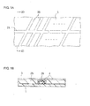
- FIGS. 1A and 1B are a plan view and an enlarged X1-X1 sectional view, respectively, which schematically illustrate a connector optical waveguide produced by a connector optical waveguide production method according to a first embodiment.
- the connector optical waveguide includes an under-cladding layer 1, cores 2A, 2B provided in a crossing pattern on a surface of the under-cladding layer 1, and an over-cladding layer 3 provided over the cores 2A, 2B.
- the cores 2A, 2B include mixed layers 4 of a mixture of a core material and an over-cladding layer material provided in portions of the cores 2A, 2B adjacent to interfaces between the cores 2A, 2B and the over-cladding layer 3.
- the crossing pattern of the cores 2A, 2B is such that a plurality of parallel cores 2B cross a single linear core 2A in the same plane.
- a planar substrate 10 (see FIG. 2A ) to be used for formation of the under-cladding layer 1 is prepared.
- Exemplary materials for the substrate 10 include glass, resins such as polyethylene terephthalates (PET) and polyethylene naphthalates (PEN), metals such as stainless steel, quartz and silicon.
- the substrate 10 has a thickness of, for example, 20 ⁇ m to 1.5 mm.
- the under-cladding layer 1 is formed on a surface of the substrate 10.
- a thermosetting resin composition or a photosensitive resin composition is used as a material for the under-cladding layer 1.
- the formation of the under-cladding layer 1 is achieved by applying the thermosetting resin composition on the surface of the substrate 10, and then heating the applied thermosetting resin composition.
- the formation of the under-cladding layer is achieved by applying the photosensitive resin composition on the surface of the substrate 10, and then exposing the applied photosensitive resin composition to radiation such as ultraviolet radiation.
- the under-cladding layer 1 has a thickness of, for example, 5 to 60 ⁇ m, preferably about 25 ⁇ m.
- the cores 2A, 2B are formed in the crossing pattern (see FIG. 1A ) on the surface of the under-cladding layer 1 by a photolithography process.
- a photosensitive resin composition which is excellent in patternability, is preferably used as a material for the cores 2A, 2B.
- the photosensitive resin composition include photosensitive epoxy resin compositions, photosensitive acryl resin compositions and photosensitive oxetanyl resin compositions, which may be used either alone or in combination.
- the cores 2A, 2B each have a trapezoidal or rectangular cross section, which ensures excellent patternability.
- the cores 2A, 2B each have a thickness (height) of, for example, 30 to 80 ⁇ m, preferably about 50 ⁇ m.
- the cores 2A, 2B each have a width of, for example, 30 to 70 ⁇ m, preferably about 50 ⁇ m.
- the crossing pattern is, for example, such that one to thirty cores 2B cross a single core 2A at a crossing angle of 30 to 90 degrees.
- the material for the cores 2A, 2B has a higher refractive index than the material for the under-cladding layer 1 and a material for the over-cladding layer 3 (see FIG. 2D ) to be described later.
- the refractive index may be adjusted, for example, by selection of the types of the materials for the under-cladding layer 1, the cores 2A, 2B and the over-cladding layer 3 and adjustment of the composition ratio of the materials.
- a material for the photosensitive resin layer 3A is a photosensitive resin composition
- examples of the photosensitive resin composition include photosensitive epoxy resin compositions, photosensitive acryl resin compositions and photosensitive oxetanyl resin compositions, which may be used either alone or in combination.
- the photosensitive resin composition may be of a solvent type which contains an organic solvent such as ethyl lactate for adjustment of the viscosity of the photosensitive resin composition, or may be of a non-solvent type which contains no organic solvent.
- the organic solvent is nonreactive with a photosensitive resin as a primary component of the photosensitive resin composition, and has a resin swelling/plasticizing effect.
- the formation of the photosensitive resin layer 3A is achieved by applying the photosensitive resin composition over the cores 2A, 2B on the surface of the under-cladding layer 1.
- a heat treatment is performed at a temperature of 70°C to 130°C, whereby mixed layers 4 are formed in portions of the cores 2A, 2B of the crossing pattern adjacent to interfaces between the cores 2A, 2B and the photosensitive resin layer 3A as shown in Fig. 2D . That is, the heat treatment causes the over-cladding layer photosensitive resin composition applied in an uncured state to penetrate into the interfacial portions of the cores 2A, 2B to be thereby mixed with the core resin material.
- the interfacial portions which are composed of a mixture of the over-cladding layer photosensitive resin composition and the core resin material, serve as the mixed layers 4.
- the thickness of each of the mixed layers 4 is controlled by the heat treatment temperature (i.e., the mixed layer thickness is increased with the heat treatment temperature).
- the mixed layer thickness is typically 2 to 20 ⁇ m. If the heat treatment temperature is lower than 70°C, it is impossible to properly form the mixed layers 4.
- the heat treatment period is preferably 1 to 20 minutes, and more preferably 5 to 10 minutes. This ensures the proper formation of the mixed layers 4, thereby further reducing an optical coupling loss occurring when components (e.g., information processing components and the like) are connected to each other via the resulting connector optical waveguide.
- components e.g., information processing components and the like
- the over-cladding layer 3 has a thickness of, for example, 5 to 60 ⁇ m, preferably about 25 ⁇ m as measured from top surfaces of the cores 2A, 2B.
- the substrate 10 is removed from the under-cladding layer 1.
- the film-shaped connector optical waveguide (see FIGS. 1A and 1B ) is produced, which includes the under-cladding layer 1, the cores 2A, 2B, the mixed layers 4 and the over-cladding layer 3.
- the refractive index of the mixed layers 4 is intermediate between the refractive index of the cores 2A, 2B and the refractive index of the over-cladding layer 3, and is lower than the refractive index of the cores 2A, 2B.
- the light transmission loss herein means a light loss occurring when the light is transmitted through the cores, and a major cause of the light transmission loss is the scattering of the light on the surfaces of the cores.
- the optical excess loss herein means a light loss occurring due to the configuration of the core pattern, e.g., a crossing core pattern, a branched core pattern, a bent core pattern or the like. In general, the light is likely to partly leak out of the cores into the cladding layer at the intersections, branch points and bent portions of the cores, and the optical loss occurs due to the leak of the light.
- the core pattern is such that the cores 2B each cross the core 2A at a single point, but may be such that three or more cores cross at a single point.
- the film-shaped connector optical waveguide has a thickness of, for example, 40 to 200 ⁇ m, preferably about 100 ⁇ m.
- the connector optical waveguide having the cores 2A, 2B arranged in the crossing pattern is usable, for example, instead of a backplane for connection between circuit boards.
- the sequence of the cores 2A, 2B optical interconnections
- the cores 2A, 2B are not arranged in a multi-level crossing pattern, it is possible to achieve the higher density integration of the optical interconnections, simplify the step of forming the optical interconnections, and reduce the thickness of the connector optical waveguide.
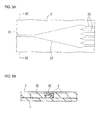
- FIGS. 3A and 3B are a plan view and an X2-X2 sectional view, respectively, which schematically illustrate a connector optical waveguide produced by a connector optical waveguide production method according to a second embodiment.
- a single core 2C is branched into a plurality of cores 2D (five cores 2D in FIG. 2A ).
- the branched pattern is such that a single core 2C having a constant width is connected at its distal end to a generally isosceles triangular portion 2E having a progressively increasing width, and the generally isosceles triangular portion 2E has a distal portion branched into a plurality of portions (five portions in FIG. 3A ) which each have a progressively decreasing width and are respectively connected to cores 2D each having a constant width.
- the other components of the connector optical waveguide are the same as in the first embodiment shown in FIGS. 1A and 1B .
- the connector optical waveguide is produced as having mixed layers 4 in portions of the cores 2C, 2E, 2D of the branched pattern adjacent to interfaces between the cores 2C, 2E, 2D and the over-cladding layer 3 by the same method as shown in FIGS. 2A to 2D .
- the provision of the mixed layers 4 prevents scattering of light on surfaces of the cores 2C, 2E, 2D to reduce the light transmission loss, and suppresses leak of light at branch points of the cores to significantly reduce the optical excess loss.
- the branched core pattern is such that the single core 2C is branched into the plurality of cores 2D via the generally isosceles triangular portion 2E, but may be such that a generally trapezoidal portion 2F is provided instead of the generally isosceles triangular portion 2E as shown in FIG. 4A .
- the branched core pattern may be a so-called Y-branched pattern such that the single core 2C is branched into two cores 2D as shown in FIG. 4B , or may include a plurality of Y-branched patterns in combination as shown in FIG. 4C .
- the connector optical waveguide including the cores 2C, 2D of the branched pattern may be used, for example, for connection between a single CPU and a plurality of memories. In this case, the same signals are simultaneously transmitted to the plurality of memories from the single CPU.
- FIGS. 5A and 5B are a plan view and an X3-X3 sectional view, respectively, which illustrate a connector optical waveguide produced by a connector optical waveguide production method according to a third embodiment.
- the connector optical waveguide has substantially the same construction as in the first embodiment shown in FIGS. 1A and 1B , except that a plurality of linear cores 2G (three cores 2G in FIG. 5A ) are provided parallel to each other.
- the connector optical waveguide is produced as having mixed layers 4 in portions of the cores 2G of the parallel pattern adjacent to interfaces between the cores 2G and the over-cladding layer 3 by the same method shown in FIGS. 2A to 2D .
- a connector optical waveguide (not shown) including cores 2A to 2D arranged in a combination of the crossing pattern and the branched pattern may be produced by a connector optical waveguide production method according to a fourth embodiment.
- the connector optical waveguides produced by the connector optical waveguide production methods according to the first to fourth embodiments are cut by means of a dicing saw or a laser so as to be properly trimmed. Then, an optical 1 waveguide connector is produced by mounting a ferrule (connecting part) having a connecting function onto any of the connector optical waveguides.
- the ferrule preferably has a configuration connectable to an MT ferrule specified by IEC 61754-5, or a PMT ferrule specified by JPCA-PE03-01-07S.
- Another exemplary method for trimming the connector optical waveguides is to pattern the under-cladding layer and the over-cladding layer by a photolithography process.
- Component A solid epoxy resin: an epoxy resin containing an aromatic ring skeleton (EPICOAT 1002 available from Mitsubishi Chemical Corporation)
- Component B solid epoxy resin: an epoxy resin containing an alicyclic skeleton (EHPE 3150 available from Daicel Chemical Industries, Ltd.)
- Component C photoacid generator: a 50% propione carbonate solution of a triarylsulfonium salt (CPI-200K available from San Apro Ltd.)
- a photosensitive resin composition was prepared as an under-cladding layer material and an over-cladding layer material by dissolving 70 parts by weight of Component A, 30 parts by weight of Component B, and 2 parts by weight of Component C in 55 parts by weight of ethyl lactate (available from Musashino Chemical Laboratory, Ltd.) with stirring at a temperature of 80°C at a stirring speed of 250 rmp for 3 hours.
- the photosensitive resin composition thus prepared had a viscosity of 1320 mPa ⁇ s as measured by a Brookfield's digital viscometer (HBDV-I+CP).
- Component D o-cresol novolak glycidyl ether (YDCN-700-10 available from Shinnittetsu Kagaku K.K.)
- a photosensitive resin composition was prepared as a core material by dissolving 100 parts by weight of Component D and 1 part by weight of Component C in 60 parts by weight of ethyl lactate (available from Musashino Chemical Laboratory, Ltd.) with stirring at a temperature of 80°C at a stirring speed of 250 rmp for 3 hours.
- the photosensitive resin composition thus prepared had a viscosity of 1900 mPa ⁇ s as measured by the digital viscometer described above.
- the under-cladding layer material was applied onto a surface of a glass substrate (available from Central Glass Co., Ltd. and having a size of 140 mm ⁇ 140 mm ⁇ 1.1 mm (thickness)) by means of a spin coater (1X-DX2 available from Mikasa Co., Ltd.) and dried at 130°C for 10 minutes to form a coating layer.
- the coating layer was entirely irradiated with ultraviolet radiation (at a wavelength of 365 nm) at a cumulative dose of 2000 mJ/cm 2 by means of an exposure machine (MA-60F available from Mikasa Co., Ltd.) and an ultra-high pressure mercury lamp (USH-250D available from Ushio Inc.) for exposure. Then, the resulting coating film was heat-treated at 130°C for 10 minutes. Thus, an under-cladding layer was formed.
- the core material was applied onto a surface of the under-cladding layer by means of the spin coater, and then dried at 130°C for 5 minutes to form a photosensitive resin layer.
- the photosensitive resin layer was exposed via a photomask by irradiation with ultraviolet radiation (at a wavelength of 365 nm) at a cumulative dose of 4000 mJ/cm 2 by means of the exposure machine and the ultra-thigh pressure mercury lamp, and then heat-treated 130°C for 15 minutes.
- a development process (dipping development process) was performed by dipping the resulting photosensitive resin layer in a developing liquid of ⁇ -butyrolactone (available from Mitsubishi Chemical Corporation) for 3 minutes, whereby an unexposed portion of the photosensitive resin layer was dissolved away.
- the resulting photosensitive resin layer was heat-treated at 120°C for 10 minutes.
- cores 2A, 2B were formed in a crossing pattern, and a core 2 was formed in a linear pattern (see FIG. 6 ).
- the crossing pattern was such that 30 parallel cores 2B crossed a single linear core 2A at an angle of 90 degrees.
- the 30 parallel cores 2B were spaced 0.2 mm from one another.
- the linear pattern was such that the single core 2 extends parallel to the linear core 2A.
- the cores 2A, 2B, 2 each had a height of 50 ⁇ m and a width of 50 ⁇ m.
- the over-cladding layer material was applied over the cores 2A, 2B, 2 onto the surface of the under-cladding layer by means of the spin coater to form an over-cladding layer formation photosensitive resin layer, and then heat-treated at 70°C for 10 minutes.
- Mixed layers 4 (see FIG. 6 ) were formed in interfaces between the cores 2A, 2B, 2 and the photosensitive resin layer by the heat treatment.
- the resulting photosensitive resin layer was exposed by irradiation with ultraviolet radiation (at a wavelength of 365 nm) at a cumulative dose of 2000 mJ/cm 2 by means of the exposure machine and the ultra-high pressure mercury lamp, and then heat-treated at 130°C for 10 minutes.
- an over-cladding layer 3 (see FIG. 6 ) was formed.
- a film-shaped connector optical waveguide was produced, which included the under-cladding layer 1, the cores 2A, 2B, 2, the mixed layers 4 and the over-cladding layer 3 as shown in Fig. 6 .
- the connector optical waveguide was bonded onto a dicing tape (UE-111AJ available from Nitto Denko Corporation), and cut to a length of 30 mm at a cutting rate of 0.3 mm/second so as to contain all intersections of the crossing pattern by means of a dicing saw (DAD522 available from Disco Corporation) and a dicing blade (NBC-Z2050 available from Disco Corporation and having a size of 50.6 ⁇ 0. 025 ⁇ 40 mm), whereby longitudinally opposite end faces of the linear core 2A of the crossing pattern and the core 2 of the linear pattern were exposed.
- a dicing tape UE-111AJ available from Nitto Denko Corporation
- a connector optical waveguide having a length of 30 mm was produced in substantially the same manner as in Example 1, except that the heat treatment (for the formation of the mixed layers) was performed at 100°C for 10 minutes before the irradiation with the ultraviolet radiation in the over-cladding layer forming step.
- a connector optical waveguide having a length of 30 mm was produced in substantially the same manner as in Example 1, except that the heat treatment (for the formation of the mixed layers) was performed at 130°C for 10 minutes before the irradiation with the ultraviolet radiation in the over-cladding layer forming step.
- a connector optical waveguide having a length of 30 mm was produced in substantially the same manner as in Example 1, except that the heat treatment (for the formation of the mixed layers) was performed at 150°C for 10 minutes before the irradiation with the ultraviolet radiation in the over-cladding layer forming step.
- a colorless transparent PET substrate (Model No. 188 of Type T60 available from TORAY Industries, Inc., and having a thickness of 188 ⁇ m) was prepared.
- a connector optical waveguide having a length of 30 mm was produced in substantially the same manner as in Example 1, except that the under-cladding layer, the cores 2A, 2B, 2, the mixed layers 4 and the over-cladding layer 3 were formed on a surface of the PET substrate.
- a connector optical waveguide having a length of 30 mm was produced in substantially the same manner as in Example 4, except that the heat treatment (for the formation of the mixed layers) was performed at 100°C for 10 minutes before the irradiation with the ultraviolet radiation in the over-cladding layer forming step.
- a connector optical waveguide having a length of 30 mm was produced in substantially the same manner as in Example 4, except that the heat treatment (for the formation of the mixed layers) was performed at 130°C for 10 minutes before the irradiation with the ultraviolet radiation in the over-cladding layer forming step.
- a colorless transparent PEN substrate (Model No. C4368 of Type Q51 available from Teijin DuPont Films Limited, and having a thickness of 188 ⁇ m) was prepared.
- a connector optical waveguide having a length of 30 mm was produced in substantially the same manner as in Example 1, except that the under-cladding layer, the cores 2A, 2B, 2, the mixed layers 4 and the over-cladding layer 3 were formed on a surface of the PEN substrate.
- a connector optical waveguide having a length of 30 mm was produced in substantially the same manner as in Example 7, except that the heat treatment (for the formation of the mixed layers) was performed at 100°C for 10 minutes before the irradiation with the ultraviolet radiation in the over-cladding layer forming step.
- a connector optical waveguide having a length of 30 mm was produced in substantially the same manner as in Example 7, except that the heat treatment (for the formation of the mixed layers) was performed at 130°C for 10 minutes before the irradiation with the ultraviolet radiation in the over-cladding layer forming step.
- a stainless steel substrate of a SUS304 foil (available from Toyo Seihaku Co., Ltd., and having a thickness of 20 ⁇ m) was prepared.
- a connector optical waveguide having a length of 30 mm was produced in substantially the same manner as in Example 1, except that the under-cladding layer, the cores 2A, 2B, 2, the mixed layers 4 and the over-cladding layer 3 were formed on a surface of the stainless steel substrate.
- a connector optical waveguide having a length of 30 mm was produced in substantially the same manner as in Example 10, except that the heat treatment (for the formation of the mixed layers) was performed at 100°C for 10 minutes before the irradiation with the ultraviolet radiation in the over-cladding layer forming step.
- a connector optical waveguide having a length of 30 mm was produced in substantially the same manner as in Example 10, except that the heat treatment (for the formation of the mixed layers) was performed at 130°C for 10 minutes before the irradiation with the ultraviolet radiation in the over-cladding layer forming step.
- a connector optical waveguide having a length of 30 mm was produced in substantially the same manner as in Example 10, except that the heat treatment (for the formation of the mixed layers) was performed at 150°C for 10 minutes before the irradiation with the ultraviolet radiation in the over-cladding layer forming step.
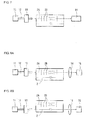
- a light intensity distribution in the linear core 2A of the crossing pattern in each of the 30-mm long connector optical waveguides of Examples 1 to 12 and Comparative Examples 1 and 4 was measured by means of a light beam measurement system (LEPAS-12 available from Hamamatsu Photonics Co. Ltd.) 14 as shown in FIG. 7 . Since it was impossible to provide the connector optical waveguides of Comparative Examples 2 and 3, the measurement was not carried out for Comparative Examples 2 and 3.
- a VCSEL O250 available from Miki Inc.
- the light emitted from the light source 11 was guided to an input end face of the core 2A via a 5- ⁇ m ⁇ graded multimode fiber 12.
- a mode scrambler (0600123 available from Diamond Co., Ltd.) 13 was disposed in the fiber 12 for proper excitation conditions.
- cores 2A, 2B, 2 are shown by broken lines, and the thicknesses of the cores 2A, 2B, 2 are indicated by the thicknesses of the broken lines.
- the percentage of the area of the mixed layer in the cross section of the core 2A was calculated based on the measurement of the light intensity distribution. The calculation results are shown below in Table 1.
- the light transmission loss (total loss) of each of the 30-mm long connector optical waveguides of Examples 1 to 12 and Comparative Examples 1 and 4 was measured by means of an optical multi-power meter (Q822 available from Advantest Corporation) 15 as shown in FIGS. 8A and 8B . Since it was impossible to provide the connector optical waveguides of Comparative Examples 2 and 3, the measurement was not carried out for Comparative Examples 2 and 3.
- the light source 11, the fiber 12 and the mode scrambler 13 described above were used for the measurement of the light transmission loss. Further, a lens 16 was disposed between an outlet end face and the optical multi-power meter 15.
- the cores 2A, 2B, 2 are indicated by broken lines
- the thicknesses of the cores 2A, 2B, 2 are indicated by the thicknesses of the broken lines.
- the light emitted from the light source 11 was inputted to the input end face of the linear core 2A of the crossing pattern via the mode scrambler 13 and outputted from the output end face.
- the outputted light was inputted to the optical multi-power meter 15 via the lens 16, and the total loss A of the single linear core 2A of the crossing pattern was measured.
- the light emitted from the light source 11 was inputted to the optical multi-power meter 15 via the mode scrambler 13, the core 2 of the linear pattern and the lens 16, and the total loss B of the core 2 of the linear pattern was measured.
- a value obtained by subtracting the total loss B of the core 2 of the linear pattern from the total loss A of the linear core 2A of the crossing pattern was defined as an optical excess loss occurring due to the crossing (crossing loss).
- the crossing losses of the connector optical waveguides are shown below in Table 1.
- a connector optical waveguide rated as excellent is indicated by “A” and a connector optical waveguide rated as particularly excellent is indicated by “AA” in Table 1. Further, a connector optical waveguide rated as inferior is indicated by “B” in Table 1.
- Example 1 (Solvent type/Crossing pattern) Material for substrate Mixed layer formation Temperature (°C) Mixed layer percentage (%) Crossing loss (dB) Comprehensive evaluation Example 1 Glass 70 35.9 2.0 A Example 2 100 62.7 0.7 AA Example 3 130 73.7 0.3 AA Comparative Example 1 150 91.5 3.0 B Example 4 PET 70 35.9 2.5 A Example 5 100 62.7 0.9 AA Example 6 130 73.7 0.5 AA Comparative Example 2 150 - - B Example 7 PEN 70 35.9 2.7 A Example 8 100 62.7 1.0 AA Example 9 130 73.7 0.4 AA Comparative Example 3 150 - - B Example 10 Stainless steel 70 35.9 2.8 A Example 11 100 62.7 0.8 AA Example 12 130 73.7 0.5 AA Comparative Example 4 150 91.5 1.0 B
- Connector optical waveguide production processes according to Examples 13 to 24 and Comparative Examples 5 to 8 were performed in substantially the same manner as in Examples 1 to 12 and Comparative Examples 1 to 4, respectively, except that cores 2C, 2D of a branched pattern and a core 2 of a linear pattern were formed as shown in FIG. 9 .
- a single linear core 2C having a constant width of 50 ⁇ m was connected at its distal end to a generally isosceles triangular portion 2E diverged at an angle of 4 degrees as having a progressively increasing width, and the generally isosceles triangular portion 2E was branched into five core portions each tapered at a taper angle of 2 degrees as having a progressively decreasing width and respectively connected to linear cores 2D each having a constant width of 50 ⁇ m.
- the cores 2C, 2D, 2 each had a height of 50 ⁇ m.
- Connector optical waveguide production processes according to Examples 25 to 36 and Comparative Examples 9 to 12 were performed in substantially the same manner as in Examples 1 to 12 and Comparative Examples 1 to 4, respectively, except that three linear cores 2G were formed parallel to each other (see FIGS. 5A and 5B ).
- the cores 2G each had a height of 50 ⁇ m and a width of 50 ⁇ m.
- under-cladding layer material and over-cladding layer material were prepared, and the same core material as used in Examples 1 to 12 and Comparative Examples 1 to 4 were prepared.
- Component B solid epoxy resin: 65 parts by weight of an epoxy resin containing an alicyclic skeleton (EHPE3150 available from Daicel Chemical Industries, Ltd.)
- Component C photoacid generator: 1 part by weight of a 50% propione carbonate solution of a triarylsulfonium salt (CPI-200K available from San Apro Ltd.)
- a photosensitive resin composition was prepared as an under-cladding layer material by dissolving Components B and C in 35 parts by weight of cyclohexanone (available from Wako Pure Chemical Industries, Ltd.) with stirring at a temperature of 80°C at a stirring speed of 250 rmp for 3 hours.
- the photosensitive resin composition thus prepared had a viscosity of 1800 mPa ⁇ s as measured by the digital viscometer described above.
- Component E liquid epoxy resin: 100 parts by weight of an epoxy resin containing an alicyclic skeleton (ADEKA RESIN EP4080E available from Adeka Corporation)
- a photosensitive resin composition was prepared as an over-cladding layer material by mixing Components E and C at a temperature of 60°C with stirring in an ultrasonic cleaner for 2 hours.
- the photosensitive resin composition thus prepared had a viscosity of 1850 mPa ⁇ s as measured by the digital viscometer described above.
- the under-cladding layer material was applied onto a surface of each of the various types of substrates used in Examples 1 to 12 and Comparative Examples 1 to 4 (see Table 4) by means of a spin coater (1X-DX2 available from Mikasa Co., Ltd.) and dried at 100°C for 5 minutes to form a coating layer.
- the coating layer was entirely irradiated with ultraviolet radiation (at a wavelength of 365 nm) at a cumulative dose of 2000 mJ/cm 2 by means of an exposure machine (MA-60F available from Mikasa Co., Ltd.) and an ultra-high pressure mercury lamp (USH-250D available from Ushio Inc.) for exposure. Then, the resulting coating film was heat-treated at 100°C for 5 minutes. Thus, an under-cladding layer was formed.
- Cores 2A, 2B of a crossing pattern and a core 2 of a linear pattern were formed in substantially the same manner as in Examples 1 to 12 and Comparative Examples 1 to 4 (see FIG. 6 ).
- the over-cladding layer material was applied over the cores 2A, 2B, 2 onto the surface of the under-cladding layer by means of the spin coater to form an over-cladding layer formation photosensitive resin layer, which was in turn heat-treated at different temperatures shown in Table 4 for 10 minutes.
- Mixed layers 4 (see FIG. 6 ) were formed in portions of the cores 2A, 2B, 2 adjacent to interfaces between the cores 2A, 2B, 2 and the photosensitive resin layer by the heat treatment.
- the resulting photosensitive resin layer was exposed by irradiation with ultraviolet radiation (at a wavelength of 365 nm) at a cumulative dose of 1000 mJ/cm 2 by means of the exposure machine and the ultra-high pressure mercury lamp, and then heat-treated at 120°C for 10 minutes.
- ultraviolet radiation at a wavelength of 365 nm
- an over-cladding layer 3 at 120°C for 10 minutes.
- Example 4 (Non-solvent type/Crossing pattern) Material for substrate Mixed layer formation Temperature (°C) Mixed layer percentage (%) Crossing loss (dB) Comprehensive evaluation Example 37 Glass 90 24.6 2.8 A Example 38 100 35.6 2.6 A Example 39 120 53.9 0.8 AA Comparative Example 13 150 87.0 0.4 B Example 40 PET 90 24.6 4.0 A Example 41 100 35.6 2.9 A Example 42 120 53.9 1.1 AA Comparative Example 14 150 - - B Example 43 PEN 90 24.6 3.2 A Example 44 100 35.6 2.7 A Example 45 120 53.9 1.0 AA Comparative Example 15 150 - - B Example 46 Stainless steel 90 24.6 3.8 A Example 47 100 35.6 2.9 A Example 48 120 53.9 1.2 AA Comparative Example 16 150 87.0 1.0 B
- Connector optical waveguide production processes according to Examples 49 to 60 and Comparative Examples 17 to 20 were performed in substantially the same manner as in Examples 37 to 48 and Comparative Examples 13 to 16, respectively, except that cores 2C, 2D of a branched pattern and a core 2 of a linear pattern were formed as in Examples 13 to 24 and Comparative Examples 5 to 8 (see FIG. 9 ).
- Connector optical waveguide production processes according to Examples 61 to 72 and Comparative Examples 21 to 24 were performed in substantially the same manner as in Examples 37 to 48 and Comparative Examples 13 to 16, respectively, except that cores 2G were formed in a linear pattern as in Examples 25 to 36 and Comparative Examples 9 to 12 (see FIGS. 5A and 5B ).
- the mixed layer percentage was reduced when the temperature of the heat treatment performed before the irradiation with the ultraviolet radiation was in the range of 70°C to 130°C in the over-cladding layer formation step in the methods of producing a connector optical waveguide including cores formed in the crossing pattern, the branched pattern or the linear pattern. Further, the cores formed in the crossing pattern each had a reduced crossing loss, and the cores formed in the branched pattern each had a reduced branching loss.
- the connector optical waveguide production processes of Examples 1 to 72 were performed by employing different heat treatment periods for the heat treatment before the irradiation with the ultraviolet radiation in the over-cladding layer formation step. As a result, a further reduced mixed layer percentage was observed when the heat treatment period was 1 to 20 minutes.
- the connector optical waveguide production method according to the present invention can be employed for production of a film-shaped connector optical waveguide which connects components (e.g., information processing components, information transmitting components and the like) to each other for light transmission between these components.
- components e.g., information processing components, information transmitting components and the like
Landscapes
- Physics & Mathematics (AREA)
- Engineering & Computer Science (AREA)
- Microelectronics & Electronic Packaging (AREA)
- General Physics & Mathematics (AREA)
- Optics & Photonics (AREA)
- Power Engineering (AREA)
- Optical Integrated Circuits (AREA)
Abstract
Description
- The present invention relates to a production method of a film-shaped optical waveguide for a connector which connects components (e.g., information processing components, information transmitting components and the like) to each other for light transmission between these components.
- Optical waveguides for connectors typically include an under-cladding layer, cores provided on a surface of the under-cladding layer and serving as optical paths, and an over-cladding layer provided over the cores.
- On the other hand, where an optical waveguide having optical interconnections (cores) of a predetermined linear pattern is provided on a surface of an electric circuit board having electric wirings in an opto-electric hybrid board, the optical waveguide is produced in the following manner. As shown in
FIG. 10A , an under-cladding layer 31 is formed on a surface of anelectric circuit board 20 opposite from an electric circuit formation surface on which anelectric circuit 21 is provided. In turn, as shown inFIG. 10B ,cores 32 are formed in a predetermined pattern on a surface of the under-claddinglayer 31 by a photolithography process. Then, as shown inFIG. 10C , an over-cladding layer photosensitive resin is applied over thecores 32 on the surface of the under-cladding layer 31 to form aphotosensitive resin layer 33A. Subsequently, a heat treatment is performed to increase the temperature of thephotosensitive resin layer 33A to evaporate a solvent contained in thephotosensitive resin layer 33A. At this time, as shown inFIG. 10D , a photosensitive resin component of thephotosensitive resin layer 33A penetrates into a surface portion of each of thecores 32 to form amixed layer 34 composed of a mixture of the photosensitive resin component and the core material. Thereafter, thephotosensitive resin layer 33A is exposed by irradiation with radiation, whereby an over-claddinglayer 33 is formed from thephotosensitive resin layer 33A. Thus, theoptical waveguide 30 is produced on the surface of theelectric circuit board 20 to provide the opto-electric hybrid board (see, for example,JP-A-2009-103827 - The refractive index of the
mixed layer 34 formed in the over-cladding layer forming step is intermediate between the refractive index of thecore 32 and the refractive index of the over-claddinglayer 33, and is lower than the refractive index of thecore 32. Therefore, light in thecore 32 is less liable to pass through themixed layer 34 formed in the surface portion of thecore 32, so that the intensity of light transmitted through themixed layer 34 is much lower than the intensity of light transmitted through a portion of thecore 32 inside themixed layer 34. This prevents scattering of light on a surface of thecore 32, thereby reducing the light transmission loss. - However, if components (e.g., information processing components or the like) are connected to each other via a film-shaped connector optical waveguide produced by forming an over-cladding layer in the same manner as the over-cladding
layer 33 of the opto-electric hybrid board described above, it is sometimes impossible to properly transmit light between the components. - To cope with this, the cause of the impossibility of the proper light transmission between the components via the film-shaped connector optical waveguide was studied. The temperature of the heat treatment of the over-cladding layer photosensitive resin for the opto-electric hybrid board (at 140°C for 30 minutes, see the paragraph [0071] in
JP-A-2009-103827 layer 34 occupies a higher percentage of thecore 32 in the opto-electric hybrid board disclosed inJP-A-2009-103827 core 32 having a higher transmission light intensity is correspondingly reduced in the cross section of thecore 32. In applications of the opto-electric hybrid board disclosed inJP-A-2009-103827 cores 32 are formed in an unbendable state on a rigid substrate (electric circuit board 20). Therefore, even if the higher transmission light intensity portion has a smaller area, there is no problem. In applications of the connector optical waveguide, however, the components are connected to each other with their optical axes slightly misaligned (it is difficult to connect the components without the misalignment). Therefore, if the higher transmission light intensity portion has a smaller area, the light coupling loss of the connector optical waveguide is increased (the proper light transmission between the components is impossible). Further, the size of the mixedlayer 34, which depends on the heat treatment temperature, is increased as the heat treatment temperature becomes higher. - In view of the foregoing, a connector optical waveguide production method is provided which reduces the optical coupling loss.
- A production method of an optical waveguide for a connector includes the steps of: forming an under-cladding layer on a surface of a substrate; forming a core in a predetermined pattern on a surface of the under-cladding layer; forming an over-cladding layer formation photosensitive resin layer over the core; performing a heat treatment at a temperature of 70°C to 130°C to form a mixed layer of a mixture of a core material and a photosensitive resin layer material in an interface between the core and the photosensitive resin layer; exposing a part of the photosensitive resin layer by irradiation with radiation to form an over-cladding layer from the exposed part; and removing the substrate from the under-cladding layer to provide a film-shaped optical waveguide connector including the under-cladding layer, the core, the mixed layer and the over-cladding layer.
- The term "film-shaped" of the film-shaped connector optical waveguide means that the optical waveguide has a thickness of 40 to 200 µm.
- Formation of the mixed layer in the connector optical waveguide production method was studied in consideration of the results of the studies conducted to reduce the optical coupling loss of the connector optical waveguide. If the temperature of the heat treatment for the formation of the mixed layer is set at a lower level on the order of 70°C to 130°C, it is possible to form the mixed layer while permitting the higher transmission light intensity portion of the core to have a sufficiently large area in the cross section of the core to ensure the function of the connector optical waveguide, and attained the present invention.
- In the connector optical waveguide production method, the temperature of the heat treatment for the formation of the mixed layer in the interface between the core and the photosensitive resin layer is set at a lower level on the order of 70°C to 130°C. This makes it possible to form the mixed layer in the interface between the core and the photosensitive resin layer while permitting the higher transmission light intensity portion of the core to have a sufficiently large area in the cross section of the core to ensure the function of the connector optical waveguide. Therefore, even if components are connected to each other via the thus produced connector optical waveguide with their optical axes slightly misaligned, the optical coupling loss can be reduced for proper light transmission between the components.
- Particularly, where the heat treatment is performed for a period of 1 to 20 minutes, the mixed layer is optimized, thereby further reducing the optical coupling loss.
- Where the core is formed in a crossing pattern, an optical excess loss occurring due to the crossing can be reduced.
- Similarly, where the core is formed in a branched pattern, an optical excess loss occurring due to the branching can be reduced.
-
-
FIGS. 1A and 1B are a plan view and an enlarged X1-X1 sectional view, respectively, which schematically illustrate a connector optical waveguide produced by a connector optical waveguide production method according to a first embodiment. -
FIGS. 2A to 2D are schematic diagrams for explaining the connector optical waveguide production method according to the first embodiment. -
FIGS. 3A and 3B are a plan view and an enlarged X2-X2 sectional view, respectively, which schematically illustrate a connector optical waveguide produced by a connector optical waveguide production method according to a second embodiment. -
FIGS. 4A to 4C are schematic plan views showing variations of a branched core pattern. -
FIGS. 5A and 5B are a plan view and an enlarged X3-X3 sectional view, respectively, which schematically illustrate a connector optical waveguide produced by a connector optical waveguide production method according to a third embodiment. -
FIG. 6 is a schematic plan view showing connector optical waveguides of Examples 1 to 12 and 37 to 48, and Comparative Examples 1 to 4 and 13 to 16. -
FIG. 7 is a diagram for explaining how to measure a light intensity distribution. -
FIGS. 8A and 8B are diagrams for explaining how to measure a light transmission loss. -
FIG. 9 is a schematic plan view showing connector optical waveguides of Examples 13 to 24 and 49 to 60, and Comparative Examples 5 to 8 and 17 to 20. -
FIGS. 10A to 10D are schematic diagrams for explaining the step of forming an optical waveguide in an opto-electric hybrid board. - With reference to the attached drawings, the present invention will hereinafter be described in detail by way of embodiments.
-
FIGS. 1A and 1B are a plan view and an enlarged X1-X1 sectional view, respectively, which schematically illustrate a connector optical waveguide produced by a connector optical waveguide production method according to a first embodiment. The connector optical waveguide includes an under-cladding layer 1,cores cladding layer 1, and an over-claddinglayer 3 provided over thecores cores mixed layers 4 of a mixture of a core material and an over-cladding layer material provided in portions of thecores cores over-cladding layer 3. In this embodiment, the crossing pattern of thecores parallel cores 2B cross a singlelinear core 2A in the same plane. - Next, the connector optical waveguide production method according to this embodiment will be described in detail.
- First, a planar substrate 10 (see
FIG. 2A ) to be used for formation of the under-cladding layer 1 is prepared. Exemplary materials for thesubstrate 10 include glass, resins such as polyethylene terephthalates (PET) and polyethylene naphthalates (PEN), metals such as stainless steel, quartz and silicon. Thesubstrate 10 has a thickness of, for example, 20 µm to 1.5 mm. - Then, as shown in
FIG. 2A , the under-cladding layer 1 is formed on a surface of thesubstrate 10. A thermosetting resin composition or a photosensitive resin composition is used as a material for the under-cladding layer 1. Where the thermosetting resin composition is used, the formation of the under-cladding layer 1 is achieved by applying the thermosetting resin composition on the surface of thesubstrate 10, and then heating the applied thermosetting resin composition. Where the photosensitive resin composition is used, on the other hand, the formation of the under-cladding layer is achieved by applying the photosensitive resin composition on the surface of thesubstrate 10, and then exposing the applied photosensitive resin composition to radiation such as ultraviolet radiation. The under-cladding layer 1 has a thickness of, for example, 5 to 60 µm, preferably about 25 µm. - In turn, as shown in
FIG.2B , thecores FIG. 1A ) on the surface of the under-cladding layer 1 by a photolithography process. A photosensitive resin composition, which is excellent in patternability, is preferably used as a material for thecores cores cores cores cores 2B cross asingle core 2A at a crossing angle of 30 to 90 degrees. - The material for the
cores cladding layer 1 and a material for the over-cladding layer 3 (seeFIG. 2D ) to be described later. The refractive index may be adjusted, for example, by selection of the types of the materials for the under-cladding layer 1, thecores over-cladding layer 3 and adjustment of the composition ratio of the materials. - Subsequently, as shown in
FIG. 2C , aphotosensitive resin layer 3A for formation of the over-cladding layer is formed over thecores cladding layer 1. A material for thephotosensitive resin layer 3A is a photosensitive resin composition, and examples of the photosensitive resin composition include photosensitive epoxy resin compositions, photosensitive acryl resin compositions and photosensitive oxetanyl resin compositions, which may be used either alone or in combination. The photosensitive resin composition may be of a solvent type which contains an organic solvent such as ethyl lactate for adjustment of the viscosity of the photosensitive resin composition, or may be of a non-solvent type which contains no organic solvent. The organic solvent is nonreactive with a photosensitive resin as a primary component of the photosensitive resin composition, and has a resin swelling/plasticizing effect. The formation of thephotosensitive resin layer 3A is achieved by applying the photosensitive resin composition over thecores cladding layer 1. - In turn, a heat treatment is performed at a temperature of 70°C to 130°C, whereby
mixed layers 4 are formed in portions of thecores cores photosensitive resin layer 3A as shown inFig. 2D . That is, the heat treatment causes the over-cladding layer photosensitive resin composition applied in an uncured state to penetrate into the interfacial portions of thecores mixed layers 4 is controlled by the heat treatment temperature (i.e., the mixed layer thickness is increased with the heat treatment temperature). The mixed layer thickness is typically 2 to 20 µm. If the heat treatment temperature is lower than 70°C, it is impossible to properly form the mixed layers 4. - The heat treatment period is preferably 1 to 20 minutes, and more preferably 5 to 10 minutes. This ensures the proper formation of the
mixed layers 4, thereby further reducing an optical coupling loss occurring when components (e.g., information processing components and the like) are connected to each other via the resulting connector optical waveguide. - After the
mixed layers 4 are formed in this manner, thephotosensitive resin layer 3A is exposed by irradiation with radiation, whereby themixed layers 4 and the other portion of thephotosensitive resin layer 3A are cured. Thus, theover-cladding layer 3 is formed. Theover-cladding layer 3 has a thickness of, for example, 5 to 60 µm, preferably about 25 µm as measured from top surfaces of thecores - Then, the
substrate 10 is removed from the under-cladding layer 1. Thus, the film-shaped connector optical waveguide (seeFIGS. 1A and 1B ) is produced, which includes the under-cladding layer 1, thecores mixed layers 4 and theover-cladding layer 3. In the connector optical waveguide, the refractive index of themixed layers 4 is intermediate between the refractive index of thecores over-cladding layer 3, and is lower than the refractive index of thecores cores mixed layers 4 provided in the interfacial portions of thecores mixed layers 4 is much lower than the intensity of light transmitted through portions of thecores cores mixed layers 4 suppresses leak of light at intersections of thecores - The light transmission loss herein means a light loss occurring when the light is transmitted through the cores, and a major cause of the light transmission loss is the scattering of the light on the surfaces of the cores. The optical excess loss herein means a light loss occurring due to the configuration of the core pattern, e.g., a crossing core pattern, a branched core pattern, a bent core pattern or the like. In general, the light is likely to partly leak out of the cores into the cladding layer at the intersections, branch points and bent portions of the cores, and the optical loss occurs due to the leak of the light.
- In the first embodiment, the core pattern is such that the
cores 2B each cross thecore 2A at a single point, but may be such that three or more cores cross at a single point. The film-shaped connector optical waveguide has a thickness of, for example, 40 to 200 µm, preferably about 100 µm. - The connector optical waveguide having the
cores cores cores -
FIGS. 3A and 3B are a plan view and an X2-X2 sectional view, respectively, which schematically illustrate a connector optical waveguide produced by a connector optical waveguide production method according to a second embodiment. In the connector optical waveguide, asingle core 2C is branched into a plurality ofcores 2D (fivecores 2D inFIG. 2A ). In this embodiment, the branched pattern is such that asingle core 2C having a constant width is connected at its distal end to a generally isoscelestriangular portion 2E having a progressively increasing width, and the generally isoscelestriangular portion 2E has a distal portion branched into a plurality of portions (five portions inFIG. 3A ) which each have a progressively decreasing width and are respectively connected tocores 2D each having a constant width. The other components of the connector optical waveguide are the same as in the first embodiment shown inFIGS. 1A and 1B . - In this embodiment, the connector optical waveguide is produced as having
mixed layers 4 in portions of thecores cores over-cladding layer 3 by the same method as shown inFIGS. 2A to 2D . The provision of themixed layers 4 prevents scattering of light on surfaces of thecores - In the second embodiment, the branched core pattern is such that the
single core 2C is branched into the plurality ofcores 2D via the generally isoscelestriangular portion 2E, but may be such that a generallytrapezoidal portion 2F is provided instead of the generally isoscelestriangular portion 2E as shown inFIG. 4A . Further, the branched core pattern may be a so-called Y-branched pattern such that thesingle core 2C is branched into twocores 2D as shown inFIG. 4B , or may include a plurality of Y-branched patterns in combination as shown inFIG. 4C . - The connector optical waveguide including the
cores -
FIGS. 5A and 5B are a plan view and an X3-X3 sectional view, respectively, which illustrate a connector optical waveguide produced by a connector optical waveguide production method according to a third embodiment. The connector optical waveguide has substantially the same construction as in the first embodiment shown inFIGS. 1A and 1B , except that a plurality oflinear cores 2G (threecores 2G inFIG. 5A ) are provided parallel to each other. - In this embodiment, the connector optical waveguide is produced as having
mixed layers 4 in portions of thecores 2G of the parallel pattern adjacent to interfaces between thecores 2G and theover-cladding layer 3 by the same method shown inFIGS. 2A to 2D . - A connector optical waveguide (not shown) including
cores 2A to 2D arranged in a combination of the crossing pattern and the branched pattern may be produced by a connector optical waveguide production method according to a fourth embodiment. - The connector optical waveguides produced by the connector optical waveguide production methods according to the first to fourth embodiments are cut by means of a dicing saw or a laser so as to be properly trimmed. Then, an optical 1 waveguide connector is produced by mounting a ferrule (connecting part) having a connecting function onto any of the connector optical waveguides. The ferrule preferably has a configuration connectable to an MT ferrule specified by IEC 61754-5, or a PMT ferrule specified by JPCA-PE03-01-07S. Another exemplary method for trimming the connector optical waveguides is to pattern the under-cladding layer and the over-cladding layer by a photolithography process.
- Next, Inventive Examples will be described in conjunction with Comparative Examples. It should be understood that the present invention be not limited to these inventive examples.
- Component A (solid epoxy resin): an epoxy resin containing an aromatic ring skeleton (EPICOAT 1002 available from Mitsubishi Chemical Corporation)
Component B (solid epoxy resin): an epoxy resin containing an alicyclic skeleton (EHPE 3150 available from Daicel Chemical Industries, Ltd.)
Component C (photoacid generator): a 50% propione carbonate solution of a triarylsulfonium salt (CPI-200K available from San Apro Ltd.) - A photosensitive resin composition was prepared as an under-cladding layer material and an over-cladding layer material by dissolving 70 parts by weight of Component A, 30 parts by weight of Component B, and 2 parts by weight of Component C in 55 parts by weight of ethyl lactate (available from Musashino Chemical Laboratory, Ltd.) with stirring at a temperature of 80°C at a stirring speed of 250 rmp for 3 hours. The photosensitive resin composition thus prepared had a viscosity of 1320 mPa·s as measured by a Brookfield's digital viscometer (HBDV-I+CP).
- A photosensitive resin composition was prepared as a core material by dissolving 100 parts by weight of Component D and 1 part by weight of Component C in 60 parts by weight of ethyl lactate (available from Musashino Chemical Laboratory, Ltd.) with stirring at a temperature of 80°C at a stirring speed of 250 rmp for 3 hours. The photosensitive resin composition thus prepared had a viscosity of 1900 mPa·s as measured by the digital viscometer described above.
- The under-cladding layer material was applied onto a surface of a glass substrate (available from Central Glass Co., Ltd. and having a size of 140 mm × 140 mm × 1.1 mm (thickness)) by means of a spin coater (1X-DX2 available from Mikasa Co., Ltd.) and dried at 130°C for 10 minutes to form a coating layer. In turn, the coating layer was entirely irradiated with ultraviolet radiation (at a wavelength of 365 nm) at a cumulative dose of 2000 mJ/cm2 by means of an exposure machine (MA-60F available from Mikasa Co., Ltd.) and an ultra-high pressure mercury lamp (USH-250D available from Ushio Inc.) for exposure. Then, the resulting coating film was heat-treated at 130°C for 10 minutes. Thus, an under-cladding layer was formed.
- Next, the core material was applied onto a surface of the under-cladding layer by means of the spin coater, and then dried at 130°C for 5 minutes to form a photosensitive resin layer. In turn, the photosensitive resin layer was exposed via a photomask by irradiation with ultraviolet radiation (at a wavelength of 365 nm) at a cumulative dose of 4000 mJ/cm2 by means of the exposure machine and the ultra-thigh pressure mercury lamp, and then heat-treated 130°C for 15 minutes. Thereafter, a development process (dipping development process) was performed by dipping the resulting photosensitive resin layer in a developing liquid of γ-butyrolactone (available from Mitsubishi Chemical Corporation) for 3 minutes, whereby an unexposed portion of the photosensitive resin layer was dissolved away. Then, the resulting photosensitive resin layer was heat-treated at 120°C for 10 minutes. Thus,
cores core 2 was formed in a linear pattern (seeFIG. 6 ). - The crossing pattern was such that 30
parallel cores 2B crossed a singlelinear core 2A at an angle of 90 degrees. The 30parallel cores 2B were spaced 0.2 mm from one another. The linear pattern was such that thesingle core 2 extends parallel to thelinear core 2A. Thecores - The over-cladding layer material was applied over the
cores FIG. 6 ) were formed in interfaces between thecores FIG. 6 ) was formed. - Thereafter, the glass substrate was removed from the under-cladding layer. Thus, a film-shaped connector optical waveguide was produced, which included the under-
cladding layer 1, thecores mixed layers 4 and theover-cladding layer 3 as shown inFig. 6 . Then, the connector optical waveguide was bonded onto a dicing tape (UE-111AJ available from Nitto Denko Corporation), and cut to a length of 30 mm at a cutting rate of 0.3 mm/second so as to contain all intersections of the crossing pattern by means of a dicing saw (DAD522 available from Disco Corporation) and a dicing blade (NBC-Z2050 available from Disco Corporation and having a size of 50.6 × 0. 025 × 40 mm), whereby longitudinally opposite end faces of thelinear core 2A of the crossing pattern and thecore 2 of the linear pattern were exposed. - A connector optical waveguide having a length of 30 mm was produced in substantially the same manner as in Example 1, except that the heat treatment (for the formation of the mixed layers) was performed at 100°C for 10 minutes before the irradiation with the ultraviolet radiation in the over-cladding layer forming step.
- A connector optical waveguide having a length of 30 mm was produced in substantially the same manner as in Example 1, except that the heat treatment (for the formation of the mixed layers) was performed at 130°C for 10 minutes before the irradiation with the ultraviolet radiation in the over-cladding layer forming step.
- A connector optical waveguide having a length of 30 mm was produced in substantially the same manner as in Example 1, except that the heat treatment (for the formation of the mixed layers) was performed at 150°C for 10 minutes before the irradiation with the ultraviolet radiation in the over-cladding layer forming step.
- A colorless transparent PET substrate (Model No. 188 of Type T60 available from TORAY Industries, Inc., and having a thickness of 188 µm) was prepared. A connector optical waveguide having a length of 30 mm was produced in substantially the same manner as in Example 1, except that the under-cladding layer, the
cores mixed layers 4 and theover-cladding layer 3 were formed on a surface of the PET substrate. - A connector optical waveguide having a length of 30 mm was produced in substantially the same manner as in Example 4, except that the heat treatment (for the formation of the mixed layers) was performed at 100°C for 10 minutes before the irradiation with the ultraviolet radiation in the over-cladding layer forming step.
- A connector optical waveguide having a length of 30 mm was produced in substantially the same manner as in Example 4, except that the heat treatment (for the formation of the mixed layers) was performed at 130°C for 10 minutes before the irradiation with the ultraviolet radiation in the over-cladding layer forming step.
- An attempt was made to produce a connector optical waveguide in substantially the same manner as in Example 4, except that the heat treatment (for the formation of the mixed layers) was performed at 150°C for 10 minutes before the irradiation with the ultraviolet radiation in the over-cladding layer forming step. However, it was impossible to produce the connector optical waveguide, because a laminate including the PET substrate, the under-cladding layer, the
cores - A colorless transparent PEN substrate (Model No. C4368 of Type Q51 available from Teijin DuPont Films Limited, and having a thickness of 188 µm) was prepared. A connector optical waveguide having a length of 30 mm was produced in substantially the same manner as in Example 1, except that the under-cladding layer, the
cores mixed layers 4 and theover-cladding layer 3 were formed on a surface of the PEN substrate. - A connector optical waveguide having a length of 30 mm was produced in substantially the same manner as in Example 7, except that the heat treatment (for the formation of the mixed layers) was performed at 100°C for 10 minutes before the irradiation with the ultraviolet radiation in the over-cladding layer forming step.
- A connector optical waveguide having a length of 30 mm was produced in substantially the same manner as in Example 7, except that the heat treatment (for the formation of the mixed layers) was performed at 130°C for 10 minutes before the irradiation with the ultraviolet radiation in the over-cladding layer forming step.
- An attempt was made to produce a connector optical waveguide in substantially the same manner as in Example 7, except that the heat treatment (for the formation of the mixed layers) was performed at 150°C for 10 minutes before the irradiation with the ultraviolet radiation in the over-cladding layer forming step. However, it was impossible to produce the connector optical waveguide, because a laminate including the PEN substrate, the under-cladding layer, the
cores - A stainless steel substrate of a SUS304 foil (available from Toyo Seihaku Co., Ltd., and having a thickness of 20 µm) was prepared. A connector optical waveguide having a length of 30 mm was produced in substantially the same manner as in Example 1, except that the under-cladding layer, the
cores mixed layers 4 and theover-cladding layer 3 were formed on a surface of the stainless steel substrate. - A connector optical waveguide having a length of 30 mm was produced in substantially the same manner as in Example 10, except that the heat treatment (for the formation of the mixed layers) was performed at 100°C for 10 minutes before the irradiation with the ultraviolet radiation in the over-cladding layer forming step.
- A connector optical waveguide having a length of 30 mm was produced in substantially the same manner as in Example 10, except that the heat treatment (for the formation of the mixed layers) was performed at 130°C for 10 minutes before the irradiation with the ultraviolet radiation in the over-cladding layer forming step.
- A connector optical waveguide having a length of 30 mm was produced in substantially the same manner as in Example 10, except that the heat treatment (for the formation of the mixed layers) was performed at 150°C for 10 minutes before the irradiation with the ultraviolet radiation in the over-cladding layer forming step.
- A light intensity distribution in the
linear core 2A of the crossing pattern in each of the 30-mm long connector optical waveguides of Examples 1 to 12 and Comparative Examples 1 and 4 was measured by means of a light beam measurement system (LEPAS-12 available from Hamamatsu Photonics Co. Ltd.) 14 as shown inFIG. 7 . Since it was impossible to provide the connector optical waveguides of Comparative Examples 2 and 3, the measurement was not carried out for Comparative Examples 2 and 3. A VCSEL (OP250 available from Miki Inc.) capable of emitting light at a wavelength of 850 nm was used as alight source 11. The light emitted from thelight source 11 was guided to an input end face of thecore 2A via a 5-µmφ gradedmultimode fiber 12. Further, a mode scrambler (0600123 available from Diamond Co., Ltd.) 13 was disposed in thefiber 12 for proper excitation conditions. InFIG. 7 ,cores cores - The percentage of the area of the mixed layer in the cross section of the
core 2A was calculated based on the measurement of the light intensity distribution. The calculation results are shown below in Table 1. - The light transmission loss (total loss) of each of the 30-mm long connector optical waveguides of Examples 1 to 12 and Comparative Examples 1 and 4 was measured by means of an optical multi-power meter (Q822 available from Advantest Corporation) 15 as shown in
FIGS. 8A and 8B . Since it was impossible to provide the connector optical waveguides of Comparative Examples 2 and 3, the measurement was not carried out for Comparative Examples 2 and 3. Thelight source 11, thefiber 12 and themode scrambler 13 described above were used for the measurement of the light transmission loss. Further, alens 16 was disposed between an outlet end face and the opticalmulti-power meter 15. InFIGS. 8A and 8B , thecores cores - As shown in
FIG. 8A , the light emitted from thelight source 11 was inputted to the input end face of thelinear core 2A of the crossing pattern via themode scrambler 13 and outputted from the output end face. The outputted light was inputted to the opticalmulti-power meter 15 via thelens 16, and the total loss A of the singlelinear core 2A of the crossing pattern was measured. Then, as shown inFIG. 8B , the light emitted from thelight source 11 was inputted to the opticalmulti-power meter 15 via themode scrambler 13, thecore 2 of the linear pattern and thelens 16, and the total loss B of thecore 2 of the linear pattern was measured. A value obtained by subtracting the total loss B of thecore 2 of the linear pattern from the total loss A of thelinear core 2A of the crossing pattern was defined as an optical excess loss occurring due to the crossing (crossing loss). The crossing losses of the connector optical waveguides are shown below in Table 1. - In consideration of the results of the evaluation of the crossing loss and the light intensity distribution, a connector optical waveguide rated as excellent is indicated by "A" and a connector optical waveguide rated as particularly excellent is indicated by "AA" in Table 1. Further, a connector optical waveguide rated as inferior is indicated by "B" in Table 1.
Table 1 (Solvent type/Crossing pattern) Material for substrate Mixed layer formation Temperature (°C) Mixed layer percentage (%) Crossing loss (dB) Comprehensive evaluation Example 1 Glass 70 35.9 2.0 A Example 2 100 62.7 0.7 AA Example 3 130 73.7 0.3 AA Comparative Example 1 150 91.5 3.0 B Example 4 PET 70 35.9 2.5 A Example 5 100 62.7 0.9 AA Example 6 130 73.7 0.5 AA Comparative Example 2 150 - - B Example 7 PEN 70 35.9 2.7 A Example 8 100 62.7 1.0 AA Example 9 130 73.7 0.4 AA Comparative Example 3 150 - - B Example 10 Stainless steel 70 35.9 2.8 A Example 11 100 62.7 0.8 AA Example 12 130 73.7 0.5 AA Comparative Example 4 150 91.5 1.0 B - Connector optical waveguide production processes according to Examples 13 to 24 and Comparative Examples 5 to 8 were performed in substantially the same manner as in Examples 1 to 12 and Comparative Examples 1 to 4, respectively, except that
cores core 2 of a linear pattern were formed as shown inFIG. 9 . In the branched pattern, a singlelinear core 2C having a constant width of 50 µm was connected at its distal end to a generally isoscelestriangular portion 2E diverged at an angle of 4 degrees as having a progressively increasing width, and the generally isoscelestriangular portion 2E was branched into five core portions each tapered at a taper angle of 2 degrees as having a progressively decreasing width and respectively connected tolinear cores 2D each having a constant width of 50 µm. Thecores - Then, the measurement of the light intensity distribution, the calculation of the mixed layer percentage, the calculation of the optical excess loss occurring due to the branching (branching loss), and the comprehensive evaluation were carried out in the same manner as described above. The results are shown below in Table 2. In the measurement of the light intensity distribution and the calculation of the branching loss, light outputted from one of the five
branch cores 2D was inputted to the lightbeam measurement system 14 and the opticalmulti-power meter 15.Table 2 (Solvent type/Branched pattern) Material for substrate Mixed layer formation Temperature (°C) Mixed layer percentage (%) Branching loss (dB) Comprehensive evaluation Example 13 Glass 70 35.9 0.6 A Example 14 100 62.7 0.5 A Example 15 130 73.7 0.5 AA Comparative Example 5 150 91. 5 2.8 B Example 16 PET 70 35.9 0.9 A Example 17 100 62.7 0.7 A Example 18 130 73.7 0.5 AA Comparative Example 6 150 - - B Example 19 PEN 70 35.9 0.7 A Example 20 100 62.7 0.7 A Example 21 130 73.7 0.5 AA Comparative Example 7 150 - - B Example 22 Stainless steel 70 35.9 1.0 A Example 23 100 62.7 0.9 A Example 24 130 73.7 0.7 AA Comparative Example 8 150 91.5 3.4 B - Connector optical waveguide production processes according to Examples 25 to 36 and Comparative Examples 9 to 12 were performed in substantially the same manner as in Examples 1 to 12 and Comparative Examples 1 to 4, respectively, except that three
linear cores 2G were formed parallel to each other (seeFIGS. 5A and 5B ). Thecores 2G each had a height of 50 µm and a width of 50 µm. - Then, the measurement of the light intensity distribution and the calculation of the mixed layer percentage were carried out in the same manner as described above. The results are shown below in Table 3. In the measurement of the light intensity distribution, light emitted from the
light source 11 was inputted to one of thecores 2G, and light outputted from the onecore 2G was inputted to the lightbeam measurement system 14.Table 3 (Solvent type/Linear pattern) Material for substrate Mixed layer formation Temperature (°C) Mixed layer percentage (%) Example 25 Glass 70 35.9 Example 26 100 62.7 Example 27 130 73.7 Comparative Example 9 150 91.5 Example 28 PET 70 35.9 Example 29 100 62.7 Example 30 130 73.7 Comparative Example 10 150 - Example 31 PEN 70 35.9 Example 32 100 62.7 Example 33 130 73.7 Comparative Example 11 150 - Example 34 Stainless steel 70 35.9 Example 35 100 62.7 Example 36 130 73.7 Comparative Example 12 150 91.5 - The following under-cladding layer material and over-cladding layer material were prepared, and the same core material as used in Examples 1 to 12 and Comparative Examples 1 to 4 were prepared.
- Component B (solid epoxy resin): 65 parts by weight of an epoxy resin containing an alicyclic skeleton (EHPE3150 available from Daicel Chemical Industries, Ltd.)
- Component C (photoacid generator): 1 part by weight of a 50% propione carbonate solution of a triarylsulfonium salt (CPI-200K available from San Apro Ltd.)
- A photosensitive resin composition was prepared as an under-cladding layer material by dissolving Components B and C in 35 parts by weight of cyclohexanone (available from Wako Pure Chemical Industries, Ltd.) with stirring at a temperature of 80°C at a stirring speed of 250 rmp for 3 hours. The photosensitive resin composition thus prepared had a viscosity of 1800 mPa·s as measured by the digital viscometer described above.
- Component E (liquid epoxy resin): 100 parts by weight of an epoxy resin containing an alicyclic skeleton (ADEKA RESIN EP4080E available from Adeka Corporation)
- A photosensitive resin composition was prepared as an over-cladding layer material by mixing Components E and C at a temperature of 60°C with stirring in an ultrasonic cleaner for 2 hours. The photosensitive resin composition thus prepared had a viscosity of 1850 mPa·s as measured by the digital viscometer described above.
- The under-cladding layer material was applied onto a surface of each of the various types of substrates used in Examples 1 to 12 and Comparative Examples 1 to 4 (see Table 4) by means of a spin coater (1X-DX2 available from Mikasa Co., Ltd.) and dried at 100°C for 5 minutes to form a coating layer. In turn, the coating layer was entirely irradiated with ultraviolet radiation (at a wavelength of 365 nm) at a cumulative dose of 2000 mJ/cm2 by means of an exposure machine (MA-60F available from Mikasa Co., Ltd.) and an ultra-high pressure mercury lamp (USH-250D available from Ushio Inc.) for exposure. Then, the resulting coating film was heat-treated at 100°C for 5 minutes. Thus, an under-cladding layer was formed.
-
Cores core 2 of a linear pattern were formed in substantially the same manner as in Examples 1 to 12 and Comparative Examples 1 to 4 (seeFIG. 6 ). - The over-cladding layer material was applied over the
cores FIG. 6 ) were formed in portions of thecores cores FIG. 6 ) was formed. - Then, a 30-mm long connector optical waveguide was produced in the same manner as described above. The measurement of the light intensity distribution, the calculation of the mixed layer percentage, the calculation of the optical excess loss occurring due to the crossing (crossing loss), and the comprehensive evaluation were carried out in the same manner as described above. The results are shown below in Table 4.
Table 4 (Non-solvent type/Crossing pattern) Material for substrate Mixed layer formation Temperature (°C) Mixed layer percentage (%) Crossing loss (dB) Comprehensive evaluation Example 37 Glass 90 24.6 2.8 A Example 38 100 35.6 2.6 A Example 39 120 53.9 0.8 AA Comparative Example 13 150 87.0 0.4 B Example 40 PET 90 24.6 4.0 A Example 41 100 35.6 2.9 A Example 42 120 53.9 1.1 AA Comparative Example 14 150 - - B Example 43 PEN 90 24.6 3.2 A Example 44 100 35.6 2.7 A Example 45 120 53.9 1.0 AA Comparative Example 15 150 - - B Example 46 Stainless steel 90 24.6 3.8 A Example 47 100 35.6 2.9 A Example 48 120 53.9 1.2 AA Comparative Example 16 150 87.0 1.0 B - Connector optical waveguide production processes according to Examples 49 to 60 and Comparative Examples 17 to 20 were performed in substantially the same manner as in Examples 37 to 48 and Comparative Examples 13 to 16, respectively, except that
cores core 2 of a linear pattern were formed as in Examples 13 to 24 and Comparative Examples 5 to 8 (seeFIG. 9 ). - Then, the measurement of the light intensity distribution, the calculation of the mixed layer percentage, the calculation of the optical excess loss occurring due to the branching (branching loss), and the comprehensive evaluation were carried out. The results are shown below in Table 5.
Table 5 (Non-solvent type/Branched pattern Material for substrate Mixed layer formation Temperature (°C) Mixed layer percentage (%) Branching loss (dB) Comprehensive evaluation Example 49 Glass 90 24.6 0.8 A Example 50 100 35.6 0.4 AA Example 51 120 53.9 0.4 AA Comparative Example 17 150 87.0 1.5 B Example 52 PET 90 24.6 1.0 A Example 53 100 35.6 0.5 AA Example 54 120 53.9 0.5 AA Comparative Example 18 150 - - B Example 55 PEN 90 24.6 0.9 A Example 56 100 35.6 0.5 AA Example 57 120 53.9 0.5 AA Comparative Example 19 150 - - B Example 58 Stainless steel 90 24.6 1.2 A Example 59 100 35.6 0.6 AA Example 60 120 53.9 0.6 AA Comparative Example 20 150 87.0 1.9 B - Connector optical waveguide production processes according to Examples 61 to 72 and Comparative Examples 21 to 24 were performed in substantially the same manner as in Examples 37 to 48 and Comparative Examples 13 to 16, respectively, except that
cores 2G were formed in a linear pattern as in Examples 25 to 36 and Comparative Examples 9 to 12 (seeFIGS. 5A and 5B ). - Then, the measurement of the light intensity distribution and the calculation of the mixed layer percentage were carried out in the same manner as described above. The results are shown below in Table 6.
Table 6 (Non-solvent type/Linear pattern) Material for substrate Mixed layer formation Temperature (°C) Mixed layer percentage (%) Example 61 Glass 90 24.6 Example 62 100 35.6 Example 63 120 53.9 Comparative Example 21 150 87.0 Example 64 PET 90 24.6 Example 65 100 35.6 Example 66 120 53.9 Comparative Example 22 150 - Example 67 PEN 90 24.6 Example 68 100 35.6 Example 69 120 53.9 Comparative Example 23 150 - Example 70 Stainless steel 90 24.6 Example 71 100 35.6 Example 72 120 53.9 Comparative Example 24 150 87.0 - As can be understood from Tables 1 to 6, the mixed layer percentage was reduced when the temperature of the heat treatment performed before the irradiation with the ultraviolet radiation was in the range of 70°C to 130°C in the over-cladding layer formation step in the methods of producing a connector optical waveguide including cores formed in the crossing pattern, the branched pattern or the linear pattern. Further, the cores formed in the crossing pattern each had a reduced crossing loss, and the cores formed in the branched pattern each had a reduced branching loss.
- Further, the connector optical waveguide production processes of Examples 1 to 72 were performed by employing different heat treatment periods for the heat treatment before the irradiation with the ultraviolet radiation in the over-cladding layer formation step. As a result, a further reduced mixed layer percentage was observed when the heat treatment period was 1 to 20 minutes.
- The connector optical waveguide production method according to the present invention can be employed for production of a film-shaped connector optical waveguide which connects components (e.g., information processing components, information transmitting components and the like) to each other for light transmission between these components.
- Although specific forms of embodiments of the instant invention have been described above and illustrated in the accompanying drawings in order to be more clearly understood, the above description is made by way of example and not as a limitation to the scope of the instant invention. It is contemplated that various modifications apparent to one of ordinary skill in the art could be made without departing from the scope of the invention.
Claims (4)
- A production method of an optical waveguide for a connector comprising the steps of:forming an under-cladding layer on a surface of a substrate;forming a core in a predetermined pattern on a surface of the under-cladding layer;forming an over-cladding layer formation photosensitive resin layer over the core;performing a heat treatment at a temperature of 70°C to 130°C to form a mixed layer of a mixture of a core material and a photosensitive resin layer material in an interface between the core and the photosensitive resin layer;exposing a part of the photosensitive resin layer by irradiation with radiation to form an over-cladding layer from the exposed part; andremoving the substrate from the under-cladding layer to provide a film-shaped optical waveguide connector including the under-cladding layer, the core, the mixed layer and the over-cladding layer.
- The connector optical waveguide production method according to claim 1, wherein the heat treatment is performed for a period of 1 to 20 minutes.
- The connector optical waveguide production method according to claim 1 or 2, wherein the core is formed in a crossing pattern.
- The connector optical waveguide production method according to claim 1 or 2, wherein the core is formed in a branched pattern.
Applications Claiming Priority (1)
| Application Number | Priority Date | Filing Date | Title |
|---|---|---|---|
| JP2010217372A JP2012073358A (en) | 2010-09-28 | 2010-09-28 | Method for manufacturing optical waveguide for connector |
Publications (2)
| Publication Number | Publication Date |
|---|---|
| EP2434318A2 true EP2434318A2 (en) | 2012-03-28 |
| EP2434318A3 EP2434318A3 (en) | 2013-02-06 |
Family
ID=44735843
Family Applications (1)
| Application Number | Title | Priority Date | Filing Date |
|---|---|---|---|
| EP11182149A Withdrawn EP2434318A3 (en) | 2010-09-28 | 2011-09-21 | Production method of optical waveguide for connector |
Country Status (5)
| Country | Link |
|---|---|
| US (1) | US8415090B2 (en) |
| EP (1) | EP2434318A3 (en) |
| JP (1) | JP2012073358A (en) |
| KR (1) | KR101843583B1 (en) |
| CN (1) | CN102419461B (en) |
Cited By (1)
| Publication number | Priority date | Publication date | Assignee | Title |
|---|---|---|---|---|
| EP3961277A1 (en) * | 2020-08-25 | 2022-03-02 | Rohm and Haas Electronic Materials LLC | Waveguide with trapezoidal core |
Families Citing this family (4)
| Publication number | Priority date | Publication date | Assignee | Title |
|---|---|---|---|---|
| US20140119703A1 (en) * | 2012-10-26 | 2014-05-01 | Cisco Technology, Inc. | Printed Circuit Board Comprising Both Conductive Metal and Optical Elements |
| CH710969B1 (en) * | 2014-02-21 | 2019-08-30 | Dow Corning | A method of preparing an optical connector and optical devices comprising the optical connector thus prepared. |
| JP6959731B2 (en) * | 2016-11-30 | 2021-11-05 | 日東電工株式会社 | Optical-electric mixed board |
| JP7002886B2 (en) | 2017-08-22 | 2022-01-20 | 日東電工株式会社 | Optical Waveguide, Opto-Electricity Consolidation Board, and Opto-Electricity Consolidation Module |
Citations (1)
| Publication number | Priority date | Publication date | Assignee | Title |
|---|---|---|---|---|
| JP2009103827A (en) | 2007-10-22 | 2009-05-14 | Panasonic Electric Works Co Ltd | Photoelectric composite substrate and manufacturing method thereof |
Family Cites Families (28)
| Publication number | Priority date | Publication date | Assignee | Title |
|---|---|---|---|---|
| US5143577A (en) | 1991-02-08 | 1992-09-01 | Hoechst Celanese Corporation | Smooth-wall polymeric channel and rib waveguides exhibiting low optical loss |
| JPH10186187A (en) * | 1996-12-24 | 1998-07-14 | Nippon Telegr & Teleph Corp <Ntt> | Flexible optical waveguide device |
| JPH11183747A (en) | 1997-12-22 | 1999-07-09 | Nippon Telegr & Teleph Corp <Ntt> | Three-dimensional polymer optical waveguide array and method of manufacturing the same |
| JP2000241647A (en) * | 1999-02-17 | 2000-09-08 | Sony Corp | Optical component manufacturing apparatus and method, and optical component |
| CA2415700A1 (en) | 2000-07-10 | 2002-01-17 | Massachusetts Institute Of Technology | Graded index waveguide |
| DE10043267A1 (en) | 2000-08-28 | 2002-03-14 | Infineon Technologies Ag | Light waveguide arrangement has refractive index inside overlapping region that is greater than in light conducting core regions of light waveguides outside overlapping region |
| DE60008121T2 (en) | 2000-11-28 | 2004-09-16 | National University Of Ireland, Cork | Manufacture of materials for step refractive index waveguides |
| DE10103273A1 (en) | 2001-01-25 | 2002-08-01 | Sel Alcatel Ag | Optical waveguide structure, has planar waveguides, each with interruption in waveguide core intersection area at input to intersection and at output from intersection area |
| US6542684B2 (en) * | 2001-05-01 | 2003-04-01 | Corning Incorporated | Optimized multi-layer optical waveguiding system |
| JP4539031B2 (en) | 2002-05-28 | 2010-09-08 | パナソニック電工株式会社 | Manufacturing method of opto-electric hybrid board |
| KR100730320B1 (en) | 2002-05-28 | 2007-06-19 | 마츠시다 덴코 가부시키가이샤 | Material for substrate mounting optical circuit-electric circuit mixedly and substrate mounting optical circuit-electric circuit mixedly |
| US7037637B2 (en) * | 2002-07-17 | 2006-05-02 | Nitto Denko Corporation | Photosensitive polyimide resin precursor composition, optical polyimide obtained from the composition, optical waveguide using the polyimide, and process for producing the optical waveguide |
| US7776236B2 (en) | 2003-07-25 | 2010-08-17 | General Electric Company | Index contrast enhanced optical waveguides and fabrication methods |
| US7496266B2 (en) * | 2004-06-25 | 2009-02-24 | Omron Corporation | Film waveguide, method of manufacturing film waveguide, and electronic device |
| JP4388867B2 (en) * | 2004-07-22 | 2009-12-24 | 日東電工株式会社 | Optical waveguide with protective layer |
| JP2006063288A (en) * | 2004-08-30 | 2006-03-09 | Jsr Corp | Photosensitive resin composition, optical waveguide and method for producing the same |
| JP2006099009A (en) | 2004-09-30 | 2006-04-13 | Sanyo Electric Co Ltd | Optical branching device and optical coupler module |
| US7400809B2 (en) | 2004-12-10 | 2008-07-15 | General Electric Company | Optical waveguide devices and method of making the same |
| JP2007191432A (en) * | 2006-01-19 | 2007-08-02 | Nitto Denko Corp | Bisoxetane ether compound having fluorene structure, process for producing the same, and optical waveguide using the same |
| JP5000195B2 (en) * | 2006-05-09 | 2012-08-15 | 日東電工株式会社 | Bisoxetane compound and process for producing the same, and resin composition for optical waveguide and optical waveguide using the same |
| US8885994B2 (en) | 2007-11-30 | 2014-11-11 | Dow Corning Corporation | Integrated planar polymer waveguide for low-loss, low-crosstalk optical signal routing |
| JP2009276724A (en) | 2008-05-19 | 2009-11-26 | Nitto Denko Corp | Method of manufacturing optical waveguide device |
| JP4994310B2 (en) * | 2008-06-10 | 2012-08-08 | 日東電工株式会社 | Manufacturing method of optical waveguide |
| JP2010066667A (en) | 2008-09-12 | 2010-03-25 | Nitto Denko Corp | Method of manufacturing optical waveguide device |
| JP5106332B2 (en) | 2008-09-18 | 2012-12-26 | 日東電工株式会社 | Manufacturing method of optical waveguide device and optical waveguide device obtained thereby |
| JP2010091734A (en) * | 2008-10-07 | 2010-04-22 | Hitachi Chem Co Ltd | Resin composition for forming core part and resin film for forming core part using the same, and optical waveguide using these |
| JP2010117380A (en) | 2008-10-14 | 2010-05-27 | Nitto Denko Corp | Method for manufacturing light guide device |
| JP2011039489A (en) * | 2009-07-17 | 2011-02-24 | Nitto Denko Corp | Method of manufacturing optical waveguide device |
-
2010
- 2010-09-28 JP JP2010217372A patent/JP2012073358A/en active Pending
-
2011
- 2011-09-19 US US13/235,932 patent/US8415090B2/en not_active Expired - Fee Related
- 2011-09-21 EP EP11182149A patent/EP2434318A3/en not_active Withdrawn
- 2011-09-26 KR KR1020110096792A patent/KR101843583B1/en not_active Expired - Fee Related
- 2011-09-26 CN CN201110294172.0A patent/CN102419461B/en not_active Expired - Fee Related
Patent Citations (1)
| Publication number | Priority date | Publication date | Assignee | Title |
|---|---|---|---|---|
| JP2009103827A (en) | 2007-10-22 | 2009-05-14 | Panasonic Electric Works Co Ltd | Photoelectric composite substrate and manufacturing method thereof |
Cited By (1)
| Publication number | Priority date | Publication date | Assignee | Title |
|---|---|---|---|---|
| EP3961277A1 (en) * | 2020-08-25 | 2022-03-02 | Rohm and Haas Electronic Materials LLC | Waveguide with trapezoidal core |
Also Published As
| Publication number | Publication date |
|---|---|
| CN102419461B (en) | 2016-01-20 |
| US20120077129A1 (en) | 2012-03-29 |
| KR20120032432A (en) | 2012-04-05 |
| US8415090B2 (en) | 2013-04-09 |
| KR101843583B1 (en) | 2018-03-29 |
| JP2012073358A (en) | 2012-04-12 |
| EP2434318A3 (en) | 2013-02-06 |
| CN102419461A (en) | 2012-04-18 |
Similar Documents
| Publication | Publication Date | Title |
|---|---|---|
| JP5486359B2 (en) | Optical waveguide for optical connector, optical connector using the same, and method for manufacturing optical waveguide for optical connector | |
| CN102597827B (en) | Optical waveguide substrate and method for manufacturing same | |
| US8845208B2 (en) | Optical connector and method of manufacturing same | |
| KR101258036B1 (en) | Optical waveguide and the production method thereof | |
| KR101430266B1 (en) | Method for manufacturing optical waveguide | |
| US8644662B2 (en) | Optical connection structure and production method of optical waveguide to be used for the optical connection structure | |
| US20070227193A1 (en) | Process for producing optical waveguide | |
| US8415090B2 (en) | Production method of optical waveguide for connector | |
| JP2005352453A (en) | Optical fiber component, optical waveguide module, and manufacturing method | |
| JP2012168294A (en) | Manufacturing method of optical connector | |
| EP2098897B1 (en) | Method of manufacturing optical waveguide device using die cutting | |
| CN101806941A (en) | Photoelectric hybrid component and its manufacturing method | |
| US8606063B2 (en) | Manufacturing method for an optical waveguide and optical waveguide body used therefor | |
| US9182548B2 (en) | Optical waveguide production method | |
| US20090116799A1 (en) | Manufacturing method of optical waveguide device and optical waveguide device obtained thereby | |
| JP2010044279A (en) | Optical waveguide and method for manufacturing same | |
| US8586286B2 (en) | Resin composition for optical waveguide, and optical waveguide produced by using the resin composition | |
| JP2013257433A (en) | Optical waveguide and processing method of optical waveguide | |
| JP2005165133A (en) | Optical waveguide manufacturing method | |
| JP4458328B2 (en) | Optical waveguide manufacturing method | |
| JP2010032582A (en) | Method of manufacturing optical module | |
| Brusberg et al. | Electro-optical circuit boards with single-or multi-mode optical interconnects |
Legal Events
| Date | Code | Title | Description |
|---|---|---|---|
| PUAI | Public reference made under article 153(3) epc to a published international application that has entered the european phase |
Free format text: ORIGINAL CODE: 0009012 |
|
| AK | Designated contracting states |
Kind code of ref document: A2 Designated state(s): AL AT BE BG CH CY CZ DE DK EE ES FI FR GB GR HR HU IE IS IT LI LT LU LV MC MK MT NL NO PL PT RO RS SE SI SK SM TR |
|
| AX | Request for extension of the european patent |
Extension state: BA ME |
|
| PUAL | Search report despatched |
Free format text: ORIGINAL CODE: 0009013 |
|
| AK | Designated contracting states |
Kind code of ref document: A3 Designated state(s): AL AT BE BG CH CY CZ DE DK EE ES FI FR GB GR HR HU IE IS IT LI LT LU LV MC MK MT NL NO PL PT RO RS SE SI SK SM TR |
|
| AX | Request for extension of the european patent |
Extension state: BA ME |
|
| RIC1 | Information provided on ipc code assigned before grant |
Ipc: G02B 6/136 20060101AFI20130102BHEP Ipc: G02B 6/138 20060101ALI20130102BHEP |
|
| 17P | Request for examination filed |
Effective date: 20130725 |
|
| RBV | Designated contracting states (corrected) |
Designated state(s): AL AT BE BG CH CY CZ DE DK EE ES FI FR GB GR HR HU IE IS IT LI LT LU LV MC MK MT NL NO PL PT RO RS SE SI SK SM TR |
|
| STAA | Information on the status of an ep patent application or granted ep patent |
Free format text: STATUS: THE APPLICATION HAS BEEN WITHDRAWN |
|
| 18W | Application withdrawn |
Effective date: 20160502 |