EP2432057A1 - Lithium secondary battery and anode therefor - Google Patents
Lithium secondary battery and anode therefor Download PDFInfo
- Publication number
- EP2432057A1 EP2432057A1 EP11181491A EP11181491A EP2432057A1 EP 2432057 A1 EP2432057 A1 EP 2432057A1 EP 11181491 A EP11181491 A EP 11181491A EP 11181491 A EP11181491 A EP 11181491A EP 2432057 A1 EP2432057 A1 EP 2432057A1
- Authority
- EP
- European Patent Office
- Prior art keywords
- active material
- material layer
- anode
- opening
- current collector
- Prior art date
- Legal status (The legal status is an assumption and is not a legal conclusion. Google has not performed a legal analysis and makes no representation as to the accuracy of the status listed.)
- Granted
Links
- 229910052744 lithium Inorganic materials 0.000 title claims abstract description 35
- WHXSMMKQMYFTQS-UHFFFAOYSA-N Lithium Chemical compound [Li] WHXSMMKQMYFTQS-UHFFFAOYSA-N 0.000 title claims abstract description 34
- 239000011149 active material Substances 0.000 claims abstract description 99
- 230000000052 comparative effect Effects 0.000 description 18
- RYGMFSIKBFXOCR-UHFFFAOYSA-N Copper Chemical compound [Cu] RYGMFSIKBFXOCR-UHFFFAOYSA-N 0.000 description 16
- 239000010949 copper Substances 0.000 description 14
- 239000011889 copper foil Substances 0.000 description 14
- 238000004519 manufacturing process Methods 0.000 description 11
- 229910020888 Sn-Cu Inorganic materials 0.000 description 9
- 229910019204 Sn—Cu Inorganic materials 0.000 description 9
- 238000000635 electron micrograph Methods 0.000 description 9
- 230000008602 contraction Effects 0.000 description 7
- 239000000956 alloy Substances 0.000 description 5
- 229910045601 alloy Inorganic materials 0.000 description 5
- XUIMIQQOPSSXEZ-UHFFFAOYSA-N Silicon Chemical compound [Si] XUIMIQQOPSSXEZ-UHFFFAOYSA-N 0.000 description 4
- ATJFFYVFTNAWJD-UHFFFAOYSA-N Tin Chemical compound [Sn] ATJFFYVFTNAWJD-UHFFFAOYSA-N 0.000 description 4
- 229910052710 silicon Inorganic materials 0.000 description 4
- 239000010703 silicon Substances 0.000 description 4
- 239000000243 solution Substances 0.000 description 4
- OIFBSDVPJOWBCH-UHFFFAOYSA-N Diethyl carbonate Chemical compound CCOC(=O)OCC OIFBSDVPJOWBCH-UHFFFAOYSA-N 0.000 description 3
- KMTRUDSVKNLOMY-UHFFFAOYSA-N Ethylene carbonate Chemical compound O=C1OCCO1 KMTRUDSVKNLOMY-UHFFFAOYSA-N 0.000 description 3
- HEMHJVSKTPXQMS-UHFFFAOYSA-M Sodium hydroxide Chemical compound [OH-].[Na+] HEMHJVSKTPXQMS-UHFFFAOYSA-M 0.000 description 3
- 239000011248 coating agent Substances 0.000 description 3
- 238000000576 coating method Methods 0.000 description 3
- 230000007423 decrease Effects 0.000 description 3
- 238000009713 electroplating Methods 0.000 description 3
- 229910052751 metal Inorganic materials 0.000 description 3
- 239000002184 metal Substances 0.000 description 3
- -1 oxide Substances 0.000 description 3
- 238000007747 plating Methods 0.000 description 3
- 239000011800 void material Substances 0.000 description 3
- XEEYBQQBJWHFJM-UHFFFAOYSA-N Iron Chemical compound [Fe] XEEYBQQBJWHFJM-UHFFFAOYSA-N 0.000 description 2
- AFVFQIVMOAPDHO-UHFFFAOYSA-N Methanesulfonic acid Chemical compound CS(O)(=O)=O AFVFQIVMOAPDHO-UHFFFAOYSA-N 0.000 description 2
- PXHVJJICTQNCMI-UHFFFAOYSA-N Nickel Chemical compound [Ni] PXHVJJICTQNCMI-UHFFFAOYSA-N 0.000 description 2
- 229910001128 Sn alloy Inorganic materials 0.000 description 2
- 239000007864 aqueous solution Substances 0.000 description 2
- 239000012300 argon atmosphere Substances 0.000 description 2
- YCIMNLLNPGFGHC-UHFFFAOYSA-N catechol Chemical compound OC1=CC=CC=C1O YCIMNLLNPGFGHC-UHFFFAOYSA-N 0.000 description 2
- 229910052802 copper Inorganic materials 0.000 description 2
- SDFNZYMSEOUVIF-UHFFFAOYSA-N copper;methanesulfonic acid Chemical compound [Cu].CS(O)(=O)=O SDFNZYMSEOUVIF-UHFFFAOYSA-N 0.000 description 2
- 238000005520 cutting process Methods 0.000 description 2
- 238000002149 energy-dispersive X-ray emission spectroscopy Methods 0.000 description 2
- 238000011156 evaluation Methods 0.000 description 2
- 239000011888 foil Substances 0.000 description 2
- 239000011159 matrix material Substances 0.000 description 2
- 239000000203 mixture Substances 0.000 description 2
- 229920002120 photoresistant polymer Polymers 0.000 description 2
- 238000004080 punching Methods 0.000 description 2
- 239000000126 substance Substances 0.000 description 2
- UMGDCJDMYOKAJW-UHFFFAOYSA-N thiourea Chemical compound NC(N)=S UMGDCJDMYOKAJW-UHFFFAOYSA-N 0.000 description 2
- XLYOFNOQVPJJNP-UHFFFAOYSA-N water Substances O XLYOFNOQVPJJNP-UHFFFAOYSA-N 0.000 description 2
- 229930185605 Bisphenol Natural products 0.000 description 1
- OKTJSMMVPCPJKN-UHFFFAOYSA-N Carbon Chemical compound [C] OKTJSMMVPCPJKN-UHFFFAOYSA-N 0.000 description 1
- 229910001290 LiPF6 Inorganic materials 0.000 description 1
- 239000004698 Polyethylene Substances 0.000 description 1
- 229910000676 Si alloy Inorganic materials 0.000 description 1
- BQCADISMDOOEFD-UHFFFAOYSA-N Silver Chemical compound [Ag] BQCADISMDOOEFD-UHFFFAOYSA-N 0.000 description 1
- XSQUKJJJFZCRTK-UHFFFAOYSA-N Urea Natural products NC(N)=O XSQUKJJJFZCRTK-UHFFFAOYSA-N 0.000 description 1
- HCHKCACWOHOZIP-UHFFFAOYSA-N Zinc Chemical compound [Zn] HCHKCACWOHOZIP-UHFFFAOYSA-N 0.000 description 1
- 229910052782 aluminium Inorganic materials 0.000 description 1
- XAGFODPZIPBFFR-UHFFFAOYSA-N aluminium Chemical compound [Al] XAGFODPZIPBFFR-UHFFFAOYSA-N 0.000 description 1
- 230000015572 biosynthetic process Effects 0.000 description 1
- JALQQBGHJJURDQ-UHFFFAOYSA-L bis(methylsulfonyloxy)tin Chemical compound [Sn+2].CS([O-])(=O)=O.CS([O-])(=O)=O JALQQBGHJJURDQ-UHFFFAOYSA-L 0.000 description 1
- 229910052797 bismuth Inorganic materials 0.000 description 1
- JCXGWMGPZLAOME-UHFFFAOYSA-N bismuth atom Chemical compound [Bi] JCXGWMGPZLAOME-UHFFFAOYSA-N 0.000 description 1
- IISBACLAFKSPIT-UHFFFAOYSA-N bisphenol A Chemical compound C=1C=C(O)C=CC=1C(C)(C)C1=CC=C(O)C=C1 IISBACLAFKSPIT-UHFFFAOYSA-N 0.000 description 1
- 229910052799 carbon Inorganic materials 0.000 description 1
- 239000008199 coating composition Substances 0.000 description 1
- 239000012141 concentrate Substances 0.000 description 1
- 239000006185 dispersion Substances 0.000 description 1
- 230000000694 effects Effects 0.000 description 1
- 238000007772 electroless plating Methods 0.000 description 1
- 239000008151 electrolyte solution Substances 0.000 description 1
- 229910052732 germanium Inorganic materials 0.000 description 1
- GNPVGFCGXDBREM-UHFFFAOYSA-N germanium atom Chemical compound [Ge] GNPVGFCGXDBREM-UHFFFAOYSA-N 0.000 description 1
- 229910052742 iron Inorganic materials 0.000 description 1
- 150000002641 lithium Chemical class 0.000 description 1
- 230000000873 masking effect Effects 0.000 description 1
- 229940098779 methanesulfonic acid Drugs 0.000 description 1
- 238000000034 method Methods 0.000 description 1
- 238000012986 modification Methods 0.000 description 1
- 230000004048 modification Effects 0.000 description 1
- 229910052759 nickel Inorganic materials 0.000 description 1
- 238000000206 photolithography Methods 0.000 description 1
- 229920000573 polyethylene Polymers 0.000 description 1
- 238000007639 printing Methods 0.000 description 1
- 230000007261 regionalization Effects 0.000 description 1
- 229910052709 silver Inorganic materials 0.000 description 1
- 239000004332 silver Substances 0.000 description 1
- 239000002904 solvent Substances 0.000 description 1
- 238000004544 sputter deposition Methods 0.000 description 1
- 238000003756 stirring Methods 0.000 description 1
- 238000007740 vapor deposition Methods 0.000 description 1
- 229910052725 zinc Inorganic materials 0.000 description 1
- 239000011701 zinc Substances 0.000 description 1
Images


Classifications
-
- H—ELECTRICITY
- H01—ELECTRIC ELEMENTS
- H01M—PROCESSES OR MEANS, e.g. BATTERIES, FOR THE DIRECT CONVERSION OF CHEMICAL ENERGY INTO ELECTRICAL ENERGY
- H01M4/00—Electrodes
- H01M4/02—Electrodes composed of, or comprising, active material
- H01M4/13—Electrodes for accumulators with non-aqueous electrolyte, e.g. for lithium-accumulators; Processes of manufacture thereof
- H01M4/134—Electrodes based on metals, Si or alloys
-
- H—ELECTRICITY
- H01—ELECTRIC ELEMENTS
- H01M—PROCESSES OR MEANS, e.g. BATTERIES, FOR THE DIRECT CONVERSION OF CHEMICAL ENERGY INTO ELECTRICAL ENERGY
- H01M4/00—Electrodes
- H01M4/02—Electrodes composed of, or comprising, active material
- H01M4/13—Electrodes for accumulators with non-aqueous electrolyte, e.g. for lithium-accumulators; Processes of manufacture thereof
-
- H—ELECTRICITY
- H01—ELECTRIC ELEMENTS
- H01M—PROCESSES OR MEANS, e.g. BATTERIES, FOR THE DIRECT CONVERSION OF CHEMICAL ENERGY INTO ELECTRICAL ENERGY
- H01M10/00—Secondary cells; Manufacture thereof
- H01M10/05—Accumulators with non-aqueous electrolyte
- H01M10/052—Li-accumulators
-
- H—ELECTRICITY
- H01—ELECTRIC ELEMENTS
- H01M—PROCESSES OR MEANS, e.g. BATTERIES, FOR THE DIRECT CONVERSION OF CHEMICAL ENERGY INTO ELECTRICAL ENERGY
- H01M4/00—Electrodes
- H01M4/02—Electrodes composed of, or comprising, active material
- H01M4/64—Carriers or collectors
- H01M4/66—Selection of materials
- H01M4/661—Metal or alloys, e.g. alloy coatings
-
- H—ELECTRICITY
- H01—ELECTRIC ELEMENTS
- H01M—PROCESSES OR MEANS, e.g. BATTERIES, FOR THE DIRECT CONVERSION OF CHEMICAL ENERGY INTO ELECTRICAL ENERGY
- H01M4/00—Electrodes
- H01M4/02—Electrodes composed of, or comprising, active material
- H01M4/64—Carriers or collectors
- H01M4/66—Selection of materials
- H01M4/665—Composites
- H01M4/667—Composites in the form of layers, e.g. coatings
-
- H—ELECTRICITY
- H01—ELECTRIC ELEMENTS
- H01M—PROCESSES OR MEANS, e.g. BATTERIES, FOR THE DIRECT CONVERSION OF CHEMICAL ENERGY INTO ELECTRICAL ENERGY
- H01M4/00—Electrodes
- H01M4/02—Electrodes composed of, or comprising, active material
- H01M4/64—Carriers or collectors
- H01M4/70—Carriers or collectors characterised by shape or form
-
- H—ELECTRICITY
- H01—ELECTRIC ELEMENTS
- H01M—PROCESSES OR MEANS, e.g. BATTERIES, FOR THE DIRECT CONVERSION OF CHEMICAL ENERGY INTO ELECTRICAL ENERGY
- H01M4/00—Electrodes
- H01M4/02—Electrodes composed of, or comprising, active material
- H01M2004/021—Physical characteristics, e.g. porosity, surface area
-
- H—ELECTRICITY
- H01—ELECTRIC ELEMENTS
- H01M—PROCESSES OR MEANS, e.g. BATTERIES, FOR THE DIRECT CONVERSION OF CHEMICAL ENERGY INTO ELECTRICAL ENERGY
- H01M4/00—Electrodes
- H01M4/02—Electrodes composed of, or comprising, active material
- H01M2004/026—Electrodes composed of, or comprising, active material characterised by the polarity
- H01M2004/027—Negative electrodes
-
- H—ELECTRICITY
- H01—ELECTRIC ELEMENTS
- H01M—PROCESSES OR MEANS, e.g. BATTERIES, FOR THE DIRECT CONVERSION OF CHEMICAL ENERGY INTO ELECTRICAL ENERGY
- H01M4/00—Electrodes
- H01M4/02—Electrodes composed of, or comprising, active material
- H01M4/36—Selection of substances as active materials, active masses, active liquids
- H01M4/38—Selection of substances as active materials, active masses, active liquids of elements or alloys
-
- Y—GENERAL TAGGING OF NEW TECHNOLOGICAL DEVELOPMENTS; GENERAL TAGGING OF CROSS-SECTIONAL TECHNOLOGIES SPANNING OVER SEVERAL SECTIONS OF THE IPC; TECHNICAL SUBJECTS COVERED BY FORMER USPC CROSS-REFERENCE ART COLLECTIONS [XRACs] AND DIGESTS
- Y02—TECHNOLOGIES OR APPLICATIONS FOR MITIGATION OR ADAPTATION AGAINST CLIMATE CHANGE
- Y02E—REDUCTION OF GREENHOUSE GAS [GHG] EMISSIONS, RELATED TO ENERGY GENERATION, TRANSMISSION OR DISTRIBUTION
- Y02E60/00—Enabling technologies; Technologies with a potential or indirect contribution to GHG emissions mitigation
- Y02E60/10—Energy storage using batteries
Definitions
- the present invention relates to a lithium secondary battery and an anode thereof.
- the present invention also relates to a sheet useful for producing an anode of a lithium secondary battery (i.e., sheet for anode of lithium secondary battery) .
- An anode of a lithium secondary battery comprises a current collector (for example, copper foil) and an active material layer (for example, carbon, tin alloy and the like) laminated on the current collector.
- a current collector for example, copper foil
- an active material layer for example, carbon, tin alloy and the like
- expansion/contraction of the active material layer occurs since lithium enters and exits the active material layer during charge and discharge.
- the active material layer gets broken due to the stress produced by the expansion/contraction.
- the charge and discharge capacity of the lithium secondary battery decreases after many repeats of charge and discharge cycle.
- Patent document 1 describes configuration of a void (opening) with a given pattern in an active material layer to alleviate the above-mentioned stress.
- a stripe-shape shape of opening: stripe-shape
- a grid-shape shape of opening: square
- a square dot-shape shape of opening: grid-shape
- patent document 2 configuration of a void (opening) in a current collector itself in an attempt to alleviate the above-mentioned stress and prevent fracture of a current collector is described (particularly, patent document 2, Fig. 1 ) .
- charge-discharge-cycle property the performance to prevent decrease of the charge and discharge capacity due to repeated charge and discharge cycle
- the "opening of the active material layer” means a part free of an active material
- the "shape of the opening in a planar view” means a shape of the opening when the active material layer is seen from the perpendicular direction.
- a "network structure having an opening" in the active material layer means that, when the active material layer is seen from the perpendicular direction, plural openings are regularly aligned, and the periphery of the individual openings form a part covering the current collector layer (part where active material is present).
- a lithium secondary battery superior in the charge-discharge-cycle property can be produced.
- the present invention relates to an anode of a lithium secondary battery and a sheet for the anode.
- a sheet for an anode of a lithium secondary battery is a sheet used for producing "an anode of a lithium secondary battery”
- an anode of a lithium secondary battery can be produced by cutting or punching out a sheet in a desired size.
- anode is used to show a concept encompassing an anode of a lithium secondary battery and a sheet for the anode, unless particularly specified.
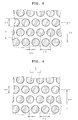
- Fig. 1 is a schematic plane view of the main part of the anode of the lithium secondary battery in the first specific example of the present invention ( Fig. 1 (A) ) and a schematic sectional view thereof ( Fig. 1 (B) )
- Fig. 2 is a schematic plane view of the main part of the anode of the lithium secondary battery in the second specific example of the present invention ( Fig. 2 (A) ) and a schematic sectional view thereof ( Fig. 2 (B) ).
- Fig. 1 (B) shows a sectional view along the line Ib-Ib in Fig. 1 (A)
- Fig. 2 (B) shows a sectional view along the line IIb-IIb in Fig. 2 (A) .
- the anode of the present invention comprises a current collector layer 1 and an active material layer 2 laminated on the current collector layer 1.
- An active material layer 2 may be formed on one surface of a current collector layer, or may be formed on both surfaces of the current collector layer.
- the current collector layer 1 does not have an opening. As a result, the current collector layer 1 can maintain its electrical resistance at a low level as well as sufficient intensity.
- the current collector layer 1 can be generally formed from an electrically conductive metal or alloy. Preferred is a metal foil or alloy foil, more preferred is a copper foil, and still more preferred is an electrolytic copper foil.
- the thickness of the current collector layer is preferably not less than 1 ⁇ m, more preferably not less than 5 ⁇ m, still more preferably not less than 8 ⁇ m, and preferably not more than 50 ⁇ m, more preferably not more than 30 ⁇ m, still more preferably not more than 20 ⁇ m.
- a network structure has an opening 2A. That is, when the active material layer 2 is seen from the perpendicular direction, plural openings 2A are regularly aligned, and the periphery of the individual openings 2A are covering parts 2B covering the current collector layer 1.
- the regular alignment of the openings 2A in the network structure is zigzag alignment, matrix alignment and the like, with preference given to zigzag alignment.
- openings 2A are aligned in a zigzag manner.
- the shape of the opening in the active material layer in a planar view is a substantially regular polygon of pentagon or above and/or a substantial circle.
- the "substantially regular polygon” means a polygon wherein the length of the longest side is not more than 1.1 times the length of the shortest side, and includes, besides regular polygons, polygons similar to regular polygons.
- the length of the longest side of a substantially regular polygon is preferably not more than 1.05 times the length of the shortest side, and the substantially regular polygon is more preferably a regular polygon.
- the "substantial circle” means an ellipse or oval wherein the major axis thereof (long axis) is not more than 1.1 times the length of the minor axis (short axis), and includes circles.
- the major axis of the substantial circle is preferably not more than 1.05 times the length of the minor axis, and the substantial circle is more preferably a circle.
- the shape of the opening 2A is a regular hexagon
- the shape of the opening 2A is a circle.
- the opening in the active material layer is a substantially regular polygon of pentagon or above and/or a substantial circle (the following Examples 1 - 12), the charge-discharge-cycle property of the lithium secondary battery can be improved, as compared to when the opening is square as described in patent document 1 (following Comparative Examples 2 and 3). While the mechanism thereof is not certain, it is assumed since a substantially regular polygon of pentagon or above has more corners than do squares (rectangles), at which the stress is considered to concentrate, the concentration of stress is reduced, and particularly, the breakage of the active material layer is further prevented.
- the substantial circle can be considered to have an infinitely increasing number of corners of the substantially regular polygon, and therefore, even a substantial circle is considered to reduce the stress concentration.
- the substantially regular polygon of pentagon or above is preferably a substantially regular hexagon and/or substantially regular octagon, more preferably substantially regular hexagon.
- the shape of the opening in the active material layer is preferably at least one selected from the group consisting of a substantially regular hexagon, a substantially regular octagon and a substantial circle, more preferably a substantially regular hexagon (particularly a regular hexagon) and/or a substantial circle (particularly a circle).
- the shape of the opening is more preferably a substantially regular hexagon (particularly a regular hexagon).
- the shape of the opening in the active material layer be basically a single shape (namely, plural openings have the same shape).
- two or more kinds of openings having different shapes may also be present.
- an opening of a substantially regular hexagon and an opening of a substantial circle may be present, and an opening of a substantially regular hexagon and an opening of a substantially regular octagon may be present.
- the longest distance across the corners of the opening which is a substantially regular polygon (A1 in Fig. 1 (A) ), is preferably not less than 1 ⁇ m, more preferably not less than 50 ⁇ m, still more preferably not less than 100 ⁇ m, and preferably not more than 1000 ⁇ m, more preferably not more than 900 ⁇ m, more preferably not more than 800 ⁇ m.
- the diameter or long axis (A2 in Fig.
- 2 (A) ) of the opening which is a substantial circle, is preferably not less than 1 ⁇ m, more preferably not less than 50 ⁇ m, still more preferably not less than 100 ⁇ m, and preferably not more than 1000 ⁇ m, more preferably not more than 900 ⁇ m, still more preferably not more than 800 ⁇ m.
- the active material layer preferably has uniform property in the entirety thereof.
- the maximum length (maximum distance across corners, or diameter or long axis) of the maximum opening in the active material layer is preferably not more than 2.0 times, more preferably not more than 1.5 times, the maximum length (maximum distance across corners, or diameter or long axis) of the minimum opening, wherein each opening more preferably has substantially the same size. That "each opening has substantially the same size” means the difference in the size of each opening is within the range of production error. In actual production, even if the openings are set to the same size, the size dispersion may occur due to a production error.
- the minimum width of the covering part of the active material layer is preferably not less than 1 ⁇ m, more preferably not less than 10 ⁇ m, still more preferably not less than 20 ⁇ m, and preferably not more than 500 ⁇ m, more preferably not more than 300 ⁇ m, still more preferably not more than 100 ⁇ m.
- the minimum width of the covering part means the smallest distance between adjacent two openings (e.g., B1 in Fig. 1 (A) , B2 in Fig. 2 (A) ).
- the covering rate is preferably not less than 5 area %, more preferably not less than 10 area %, more preferably not less than 15 area %, and preferably not more than 70 area %, more preferably not more than 65 area %, more preferably not more than 60 area %.
- the thickness of the active material layer is preferably not less than 1 ⁇ m, more preferably not less than 3 ⁇ m, still more preferably not less than 5 ⁇ m, and preferably not more than 100 ⁇ m, more preferably not more than 80 ⁇ m, still more preferably not more than 60 ⁇ m.
- a simple substance, oxide, alloy or eutectoid of tin, or a mixture thereof, or a simple substance, oxide, alloy or eutectoid of silicon, or a mixture thereof is preferable.
- the elements other than tin and silicon to be contained in the aforementioned alloy or eutectoid include copper, silver, bismuth, nickel, zinc, aluminum, iron and germanium and the like. Of these, copper is preferable.
- the amount of the elements other tin and silicon to be contained in the total active material of a lithium secondary battery to secure sufficient charge and discharge capacity is preferably not more than 50 wt%, more preferably not more than 40 wt%, still more preferably not more than 30 wt%.
- Tin alloy or eutectoid may contain silicon, and silicon alloy or eutectoid may contain tin.
- the sheet for anode of the present invention can be produced by forming an active material layer, having openings formed by a known pattern formation method, on a current collector layer.
- a resist film having openings and covering parts with shapes reverse to those of the active material layer is formed on a current collector layer by photolithography, an active material layer is formed thereon by electroplating, electroless plating, sputtering, vapor deposition, coating or printing and the like, and then, the resist film is removed to form openings of the active material layer, whereby a sheet for anode can be produced.
- An active material layer having openings formed in a given pattern can also be produced by pattern coating or masking coating using a coating composition containing an active material.
- the anode of the present invention can be produced by cutting or punching out a sheet for anode produced as mentioned above to a desired size by a known means.
- the present invention further provides a lithium secondary battery containing the above-mentioned anode.
- the lithium secondary battery of the present invention characteristically contains the above-mentioned anode, and other constitution is not particularly limited.
- the constitution of the lithium secondary battery and the production method thereof are known and are described, for example, in patent documents 1 and 2 and the like. Examples
- a negative resist film (thickness: 25 ⁇ m) was laminated on an electrolytic copper foil (thickness: 20 ⁇ m).
- the resist film was exposed and developed to form a developed resist film (shape of covering part: regular hexagon) with a pattern inverted to the photomask.
- the electrolytic copper foil having the developed resist film was immersed in a plating solution (aqueous solution containing tin(II) methanesulfonate: 39 g/L, copper(II) methanesulfonate: 6.6 g/L, methanesulfonic acid: 100 g/L, bisphenol: 5 g/L, thiourea: 10 g/L, catechol 1 g/L), and electroplating was carried out to form an Sn-Cu eutectoid plated layer (thickness: 10 ⁇ m) on the electrolytic copper foil.
- a plating solution aqueous solution containing tin(II) methanesulfonate: 39 g/L, copper(II) methanesulfonate: 6.6 g/L, methanesulfonic acid: 100 g/L, bisphenol: 5 g/L, thiourea: 10 g/L, catechol 1 g/L
- the electroplating was carried out while adjusting the temperature of the plating solution to 30°C and stirring with a stirrer for 20 min at current density of 1 A/dm 2 .
- the electrolytic copper foil having the Sn-Cu eutectoid plated layer was washed with water, and the developed resist film was detached with 3 - 5 wt% NaOH aqueous solution and further washed with water to give an electrolytic copper foil (current collector layer) having the Sn-Cu eutectoid plated layer (active material layer), wherein regular hexagon openings were aligned in a zigzag manner; that is, a sheet for anode having an active material layer with the network structure shown in Fig. 1 (A) was produced.
- each part (A1, B1, C1 and D1 in Fig. 1 (A) ) of the active material layer, and the amount of Cu in the active material layer are shown in the following Table 1.
- the size of each part of the active material layer was calculated from an electron micrograph taken by an electron microscope: "JSM-6390A” manufactured by JEOL, and the amount of Cu in the active material layer was measured by EDX (energy dispersive X-ray spectroscopy).
- EDX energy dispersive X-ray spectroscopy
- Example 6 In the same manner as in Example 2 except that the concentration of copper(II) methanesulfonate in the plating solution was changed to 0 (Example 6), 3.3 g/L (Example 7), 5.0 g/L (Example 8) or 6.6 g/L (Example 9), an electrolytic copper foil (current collector layer, thickness: 20 ⁇ m) having an Sn plated layer or Sn-Cu eutectoid plated layer (active material layer, thickness: 10 ⁇ m), wherein regular hexagon openings were aligned in a zigzag manner; that is, a sheet for anode having an active material layer with a network structure shown in Fig. 1 (A) , was produced.
- the size and covering rate of each part (A1, B1, C1 and D1 in Fig. 1 (A) ) of the active material layer, and the amount of Cu in the active material layer are shown in the following Table 1.
- Comparative Example 1 Production of sheet for anode having active material layer with circular covering parts
- Fig. 5 is a schematic plane view of the main part of the sheet for anode.
- the circular covering part 2B is aligned in a zigzag manner, and the periphery of each covering part 2B is an opening 2A.
- a photomask of the shape and size shown in Fig. 7 and Table 4 (in Fig. 7 , symbol 3 shows a translucent part, and symbol 4 shows a light shielding part.) was used, an electrolytic copper foil (current collector layer, thickness: 20 ⁇ m) having an Sn-Cu eutectoid plated layer (active material layer, thickness: 10 ⁇ m); that is, a sheet for anode, was produced.
- Fig. 8 is a schematic plane view of the main part of the sheet for anode. In the sheet for anode, square openings 2A are aligned in a matrix. The size and covering rate of each part (A4, B4 and C4 in Fig. 8 ) of the active material layer, and the amount of Cu in the active material layer are shown in Table 4.
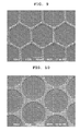
- an electron micrograph of the sheet for anode, produced in Comparative Example 2 is shown in Fig. 12 .
- Table 1 Shape of opening in active material layer regular hexagon Example size of photomask (mm) size of active material layer (mm) covering rate (area %) Cu amount (wt%) relative discharged capacity a1 b1 c1 d1 A1 B1 C1 D1 1 0.3 0.03 0.29 0.50 0.29 0.029 0.28 0.48 19 16.3 127 2 0.3 0.05 0.31 0.54 0.30 0.046 0.30 0.52 29 15.4 123 3 0.3 0.10 0.36 0.62 0.30 0.12 0.35 0.60 47 13.3 129 4 0.1 0.03 0.12 0.20 0.12 0.025 0.11 0.20 44 12.0 103 5 0.5 0.03 0.46 0.80 0.48 0.028 0.44 0.77 12 15.2 108 6 0.3 0.05 0.31 0.54 0.30 0.040 0.30 0.54 29 0 106 7 0.30 0.044 0.31 0.54 29 10.1 100 8 0.31 0.046 0.32 0.56 29 22.8 106 9 0.30 0.044 0.31 0.54 29 37.7 103
- Table 2 Shape of opening in active material layer circle Example size of photomask (mm) size of active material layer (mm) covering rate (area %) Cu amount (wt%) relative discharged capacity a2 b2 c2 d2 A2 B2 C2 D2 10 0.3 0.03 0.33 0.572 0.30 0.020 0.31 0.55 25 14.6 113 11 0.3 0.05 0.35 0.606 0.29 0.030 0.34 0.58 33 13.6 110 12 0.5 0.03 0.53 0.918 0.49 0.028 0.51 0.91 19 14.1 125
- Table 3 Shape of covering part in active material layer: circle Comparative Example size of photomask (mm) size of active material layer (mm) covering rate (area %) Cu amount (wt%) relative discharged capacity a3 b3 c3 d3 A3 B3 C3 D3 1 0.3 0.15 0.45 0.779 0.30 0.16 0.46 0.78 40 37.3 29
- Table 4 Shape of opening in active material layer square Comparative Example size of photomask (mm) size of active material layer (mm) covering rate (area %) Cu amount (wt%) relative discharged capacity a4 b4 c4 A4 B4 C4 2 0.1 0.2 0.2 0.10 0.21 0.20 55 33.6 55 3 0.1 0.5 0.5 0.10 0.50 0.50 30 33.2 33
- Example 3 coverage rate: 47%, relative discharged capacity: 129
- Example 4 coverage rate: 44%, relative discharged capacity: 103
- Comparative Example 3 with square openings covering rate: 30%, relative discharged capacity: 33
- Examples 3 and 4 showed high covering rate as compared to Comparative Example 3, and the stress due to expansion/contraction of the active material layer is considered to be higher.
Landscapes
- Chemical & Material Sciences (AREA)
- Chemical Kinetics & Catalysis (AREA)
- Electrochemistry (AREA)
- General Chemical & Material Sciences (AREA)
- Engineering & Computer Science (AREA)
- Materials Engineering (AREA)
- Manufacturing & Machinery (AREA)
- Composite Materials (AREA)
- Cell Electrode Carriers And Collectors (AREA)
- Battery Electrode And Active Subsutance (AREA)
Abstract
Description
- The present invention relates to a lithium secondary battery and an anode thereof. The present invention also relates to a sheet useful for producing an anode of a lithium secondary battery (i.e., sheet for anode of lithium secondary battery) .
- An anode of a lithium secondary battery comprises a current collector (for example, copper foil) and an active material layer (for example, carbon, tin alloy and the like) laminated on the current collector. In this lithium secondary battery, expansion/contraction of the active material layer occurs since lithium enters and exits the active material layer during charge and discharge. In addition, the active material layer gets broken due to the stress produced by the expansion/contraction. As a result, the charge and discharge capacity of the lithium secondary battery decreases after many repeats of charge and discharge cycle.
-
Patent document 1 describes configuration of a void (opening) with a given pattern in an active material layer to alleviate the above-mentioned stress. As specific shape of the active material layer, a stripe-shape (shape of opening: stripe-shape), a grid-shape (shape of opening: square) and a square dot-shape (shape of opening: grid-shape) are described (particularly,patent document 1,Fig. 3 ). - In
patent document 2, configuration of a void (opening) in a current collector itself in an attempt to alleviate the above-mentioned stress and prevent fracture of a current collector is described (particularly,patent document 2,Fig. 1 ) . -
- patent document 1:
JP-A-2004-103474 - patent document 2:
JP-A-11-233116 - In the anode proposed in the prior art (e.g., patent document 1), the performance to prevent decrease of the charge and discharge capacity due to repeated charge and discharge cycle (hereinafter abbreviated as "charge-discharge-cycle property") is not sufficient. It is therefore an object of the present invention to provide an anode of a lithium secondary battery, which can achieve a charge-discharge-cycle property superior to that of the prior art.
- The present inventors have conducted intensive studies in an attempt to achieve the above-mentioned object and completed the following invention.
- [1] An anode of a lithium secondary battery comprising a current collector layer and an active material layer laminated on the current collector layer, wherein
the current collector layer has a laminar structure without an opening ,
the active material layer has a network structure with an opening, and
the shape of the opening in a planar view is a substantially regular polygon of pentagon or above and/or a substantial circle. - [2] The anode of the above-mentioned [1], wherein the substantially regular polygon is a substantially regular hexagon.
- [3] A lithium secondary battery comprising the anode of the above-mentioned [1] or [2].
- [4] A sheet for an anode of a lithium secondary battery comprising a current collector layer and an active material layer laminated on the current collector layer, wherein
the current collector layer has a laminar structure without an opening,
the active material layer has a network structure with an opening, and
the shape of the opening in a planar view is a substantially regular polygon of pentagon or above and/or a substantial circle. - In the present invention, the "opening of the active material layer" means a part free of an active material, and the "shape of the opening in a planar view" means a shape of the opening when the active material layer is seen from the perpendicular direction. Moreover, a "network structure having an opening" in the active material layer means that, when the active material layer is seen from the perpendicular direction, plural openings are regularly aligned, and the periphery of the individual openings form a part covering the current collector layer (part where active material is present).
- Using the anode of the present invention, a lithium secondary battery superior in the charge-discharge-cycle property can be produced.
-
-
Fig. 1 (A) is a schematic plane view of the main part of the anode of the lithium secondary battery in the first specific example of the present invention, andFig. 1 (B) is a schematic sectional view along the line Ib-Ib ofFig. 1 (A) . -
Fig. 2 (A) is a schematic plane view of the main part of the anode of the lithium secondary battery in the second specific example of the present invention, andFig. 2 (B) is a schematic sectional view along the line IIb-IIb ofFig. 2 (A) . -
Fig. 3 is a schematic plane view of the photomask used in Examples 1 - 9. -
Fig. 4 is a schematic plane view of the photomask used in Examples 10 - 12. -
Fig. 5 is a schematic plane view of the photomask used in Comparative Example 1. -
Fig. 6 is a schematic plane view of the main part of the sheet for anode produced in Comparative Example 1. -
Fig. 7 is a schematic plane view of the photomask used in Comparative Examples 2 and 3. -
Fig. 8 is a schematic plane view of the main part of the sheet for anode produced in Comparative Examples 2 and 3. -
Fig. 9 is an electron micrograph of the sheet for anode produced in Example 1 (shape of opening in active material layer: regular hexagon). -
Fig. 10 is an electron micrograph of the sheet for anode produced in Example 10 (shape of opening in active material layer: circle). -
Fig. 11 is an electron micrograph of the sheet for anode produced in Comparative Example 1 (shape of covering part in active material layer: circle). -
Fig. 12 is an electron micrograph of the sheet for anode produced in Comparative Example 2 (shape of opening in active material layer: square). - The present invention relates to an anode of a lithium secondary battery and a sheet for the anode.
In the present invention, "a sheet for an anode of a lithium secondary battery" is a sheet used for producing "an anode of a lithium secondary battery", and "an anode of a lithium secondary battery" can be produced by cutting or punching out a sheet in a desired size.
In the following description, therefore, "anode" is used to show a concept encompassing an anode of a lithium secondary battery and a sheet for the anode, unless particularly specified. -
Fig. 1 is a schematic plane view of the main part of the anode of the lithium secondary battery in the first specific example of the present invention (Fig. 1 (A) ) and a schematic sectional view thereof (Fig. 1 (B) ),Fig. 2 is a schematic plane view of the main part of the anode of the lithium secondary battery in the second specific example of the present invention (Fig. 2 (A) ) and a schematic sectional view thereof (Fig. 2 (B) ).Fig. 1 (B) shows a sectional view along the line Ib-Ib inFig. 1 (A) , andFig. 2 (B) shows a sectional view along the line IIb-IIb inFig. 2 (A) . - As shown in
anode 10 inFig. 1 andFig. 2 , the anode of the present invention comprises acurrent collector layer 1 and anactive material layer 2 laminated on thecurrent collector layer 1. Anactive material layer 2 may be formed on one surface of a current collector layer, or may be formed on both surfaces of the current collector layer. - In the anode of the present invention, the
current collector layer 1 does not have an opening. As a result, thecurrent collector layer 1 can maintain its electrical resistance at a low level as well as sufficient intensity. Thecurrent collector layer 1 can be generally formed from an electrically conductive metal or alloy. Preferred is a metal foil or alloy foil, more preferred is a copper foil, and still more preferred is an electrolytic copper foil. - When the
current collector layer 1 is too thin, the internal resistance of a battery becomes high, and the load characteristic of the battery becomes low. On the other hand, when the current collector layer is too thick, the volume and weight of the battery increase and the energy density decreases. Thus, the thickness of the current collector layer is preferably not less than 1 µm, more preferably not less than 5 µm, still more preferably not less than 8 µm, and preferably not more than 50 µm, more preferably not more than 30 µm, still more preferably not more than 20 µm. - In the
active material layer 2, a network structure has an opening 2A. That is, when theactive material layer 2 is seen from the perpendicular direction, plural openings 2A are regularly aligned, and the periphery of the individual openings 2A are covering parts 2B covering thecurrent collector layer 1. Typically, the regular alignment of the openings 2A in the network structure is zigzag alignment, matrix alignment and the like, with preference given to zigzag alignment. InFig. 1 (A) andFig. 2 (A) , openings 2A are aligned in a zigzag manner. - In the anode of the present invention, the shape of the opening in the active material layer in a planar view is a substantially regular polygon of pentagon or above and/or a substantial circle.
- In the present invention, the "substantially regular polygon" means a polygon wherein the length of the longest side is not more than 1.1 times the length of the shortest side, and includes, besides regular polygons, polygons similar to regular polygons. The length of the longest side of a substantially regular polygon is preferably not more than 1.05 times the length of the shortest side, and the substantially regular polygon is more preferably a regular polygon. The "substantial circle" means an ellipse or oval wherein the major axis thereof (long axis) is not more than 1.1 times the length of the minor axis (short axis), and includes circles. The major axis of the substantial circle is preferably not more than 1.05 times the length of the minor axis, and the substantial circle is more preferably a circle. In
Fig. 1 (A) , the shape of the opening 2A is a regular hexagon, and inFig. 2 (A) , the shape of the opening 2A is a circle. - When the opening in the active material layer is a substantially regular polygon of pentagon or above and/or a substantial circle (the following Examples 1 - 12), the charge-discharge-cycle property of the lithium secondary battery can be improved, as compared to when the opening is square as described in patent document 1 (following Comparative Examples 2 and 3). While the mechanism thereof is not certain, it is assumed since a substantially regular polygon of pentagon or above has more corners than do squares (rectangles), at which the stress is considered to concentrate, the concentration of stress is reduced, and particularly, the breakage of the active material layer is further prevented. The substantial circle can be considered to have an infinitely increasing number of corners of the substantially regular polygon, and therefore, even a substantial circle is considered to reduce the stress concentration. However, the present invention is not limited to the presumed mechanism. The substantially regular polygon of pentagon or above is preferably a substantially regular hexagon and/or substantially regular octagon, more preferably substantially regular hexagon.
- The shape of the opening in the active material layer is preferably at least one selected from the group consisting of a substantially regular hexagon, a substantially regular octagon and a substantial circle, more preferably a substantially regular hexagon (particularly a regular hexagon) and/or a substantial circle (particularly a circle). The shape of the opening is more preferably a substantially regular hexagon (particularly a regular hexagon). When the opening of the active material layer is a substantial circle, as shown in
Fig. 2 (A) , the width of the covering part 2B on the periphery of opening 2A is not uniform, including a wide part and a narrow part. When the opening is a substantially regular hexagon, as shown inFig. 1 (A) , the width of the covering part 2B on the periphery of opening 2A is almost uniform, which enables formation of anactive material layer 2 having superior intensity. - It is preferable that the shape of the opening in the active material layer be basically a single shape (namely, plural openings have the same shape). However, two or more kinds of openings having different shapes may also be present. For example, an opening of a substantially regular hexagon and an opening of a substantial circle may be present, and an opening of a substantially regular hexagon and an opening of a substantially regular octagon may be present.
- When the size of the opening in the active material layer is too small, the stress due to expansion/contraction of the active material layer cannot be alleviated sufficiently. When the size of the opening is too large, charge and discharge capacity of a lithium secondary battery becomes too small. The longest distance across the corners of the opening, which is a substantially regular polygon (A1 in
Fig. 1 (A) ), is preferably not less than 1 µm, more preferably not less than 50 µm, still more preferably not less than 100 µm, and preferably not more than 1000 µm, more preferably not more than 900 µm, more preferably not more than 800 µm. In addition, the diameter or long axis (A2 inFig. 2 (A) ) of the opening, which is a substantial circle, is preferably not less than 1 µm, more preferably not less than 50 µm, still more preferably not less than 100 µm, and preferably not more than 1000 µm, more preferably not more than 900 µm, still more preferably not more than 800 µm. - While the size of each opening in the active material layer may be different, the active material layer preferably has uniform property in the entirety thereof. Thus, the maximum length (maximum distance across corners, or diameter or long axis) of the maximum opening in the active material layer is preferably not more than 2.0 times, more preferably not more than 1.5 times, the maximum length (maximum distance across corners, or diameter or long axis) of the minimum opening, wherein each opening more preferably has substantially the same size. That "each opening has substantially the same size" means the difference in the size of each opening is within the range of production error. In actual production, even if the openings are set to the same size, the size dispersion may occur due to a production error.
- When the minimum width of the covering part of the active material layer is too small, the active material layer does not adhere sufficiently to the current collector layer, and the active material may drop off after repeated charge and discharge cycles. On the other hand, when the minimum width of the covering part is too large, the stress caused by expansion/contraction of the active material layer cannot be reduced sufficiently. Therefore, the minimum width of the covering part is preferably not less than 1 µm, more preferably not less than 10 µm, still more preferably not less than 20 µm, and preferably not more than 500 µm, more preferably not more than 300 µm, still more preferably not more than 100 µm. Here, "the minimum width of the covering part" means the smallest distance between adjacent two openings (e.g., B1 in
Fig. 1 (A) , B2 inFig. 2 (A) ). - When, in the active material layer, the area ratio of the covering part relative to the total area including opening and covering part (hereinafter sometimes to be abbreviated as "covering rate") is too small, the charge and discharge capacity of the lithium secondary battery becomes too small. On the other hand, when it is too high, the stress caused by expansion/contraction of the active material layer cannot be reduced sufficiently. Hence, the covering rate is preferably not less than 5 area %, more preferably not less than 10 area %, more preferably not less than 15 area %, and preferably not more than 70 area %, more preferably not more than 65 area %, more preferably not more than 60 area %.
- When the active material layer is too thin, the charge and discharge capacity of the lithium secondary battery becomes too small. On the other hand, when it is too thick, the stress caused by expansion/contraction of the active material layer cannot be reduced sufficiently. Thus, the thickness of the active material layer (i.e., thickness of covering part) is preferably not less than 1 µm, more preferably not less than 3 µm, still more preferably not less than 5 µm, and preferably not more than 100 µm, more preferably not more than 80 µm, still more preferably not more than 60 µm.
- As an active material, a simple substance, oxide, alloy or eutectoid of tin, or a mixture thereof, or a simple substance, oxide, alloy or eutectoid of silicon, or a mixture thereof is preferable. Examples of the elements other than tin and silicon to be contained in the aforementioned alloy or eutectoid include copper, silver, bismuth, nickel, zinc, aluminum, iron and germanium and the like. Of these, copper is preferable. The amount of the elements other tin and silicon to be contained in the total active material of a lithium secondary battery to secure sufficient charge and discharge capacity is preferably not more than 50 wt%, more preferably not more than 40 wt%, still more preferably not more than 30 wt%. Tin alloy or eutectoid may contain silicon, and silicon alloy or eutectoid may contain tin.
- The sheet for anode of the present invention can be produced by forming an active material layer, having openings formed by a known pattern formation method, on a current collector layer. For example, a resist film having openings and covering parts with shapes reverse to those of the active material layer is formed on a current collector layer by photolithography, an active material layer is formed thereon by electroplating, electroless plating, sputtering, vapor deposition, coating or printing and the like, and then, the resist film is removed to form openings of the active material layer, whereby a sheet for anode can be produced. An active material layer having openings formed in a given pattern can also be produced by pattern coating or masking coating using a coating composition containing an active material.
- The anode of the present invention can be produced by cutting or punching out a sheet for anode produced as mentioned above to a desired size by a known means.
- The present invention further provides a lithium secondary battery containing the above-mentioned anode. The lithium secondary battery of the present invention characteristically contains the above-mentioned anode, and other constitution is not particularly limited. The constitution of the lithium secondary battery and the production method thereof are known and are described, for example, in
patent documents - The present invention is explained in more detail in the following by referring to Examples. However, the present invention is not limited to the following Examples, and can be practiced by making appropriate modifications and changes without substantially departing from the above or below-mentioned teaching and advantages of the present invention, all of which are encompassed in the technical scope of the present invention.
- A negative resist film (thickness: 25 µm) was laminated on an electrolytic copper foil (thickness: 20 µm). Using a photomask of the shape and size shown in
Fig. 3 and Table 1 (inFig. 3 ,symbol 3 shows a translucent part, andsymbol 4 shows a light shielding part), the resist film was exposed and developed to form a developed resist film (shape of covering part: regular hexagon) with a pattern inverted to the photomask. The electrolytic copper foil having the developed resist film was immersed in a plating solution (aqueous solution containing tin(II) methanesulfonate: 39 g/L, copper(II) methanesulfonate: 6.6 g/L, methanesulfonic acid: 100 g/L, bisphenol: 5 g/L, thiourea: 10 g/L, catechol 1 g/L), and electroplating was carried out to form an Sn-Cu eutectoid plated layer (thickness: 10 µm) on the electrolytic copper foil. The electroplating was carried out while adjusting the temperature of the plating solution to 30°C and stirring with a stirrer for 20 min at current density of 1 A/dm2. The electrolytic copper foil having the Sn-Cu eutectoid plated layer was washed with water, and the developed resist film was detached with 3 - 5 wt% NaOH aqueous solution and further washed with water to give an electrolytic copper foil (current collector layer) having the Sn-Cu eutectoid plated layer (active material layer), wherein regular hexagon openings were aligned in a zigzag manner; that is, a sheet for anode having an active material layer with the network structure shown inFig. 1 (A) was produced. The size and covering rate of each part (A1, B1, C1 and D1 inFig. 1 (A) ) of the active material layer, and the amount of Cu in the active material layer are shown in the following Table 1. The size of each part of the active material layer was calculated from an electron micrograph taken by an electron microscope: "JSM-6390A" manufactured by JEOL, and the amount of Cu in the active material layer was measured by EDX (energy dispersive X-ray spectroscopy).
In addition, the electron micrograph of the sheet for anode, produced in Example 1, is shown inFig. 9 . - In the same manner as in Example 2 except that the concentration of copper(II) methanesulfonate in the plating solution was changed to 0 (Example 6), 3.3 g/L (Example 7), 5.0 g/L (Example 8) or 6.6 g/L (Example 9), an electrolytic copper foil (current collector layer, thickness: 20 µm) having an Sn plated layer or Sn-Cu eutectoid plated layer (active material layer, thickness: 10 µm), wherein regular hexagon openings were aligned in a zigzag manner; that is, a sheet for anode having an active material layer with a network structure shown in
Fig. 1 (A) , was produced. The size and covering rate of each part (A1, B1, C1 and D1 inFig. 1 (A) ) of the active material layer, and the amount of Cu in the active material layer are shown in the following Table 1. - In the same manner as in Examples 1 - 5 except that a photomask of the shape and size shown in
Fig. 4 and Table 2 (inFig. 4 ,symbol 3 shows a translucent part, andsymbol 4 shows a light shielding part) was used, an electrolytic copper foil (current collector layer, thickness: 20 µm) having an Sn-Cu eutectoid plated layer (active material layer, thickness: 10 µm), wherein circle openings were aligned in a zigzag manner; that is, a sheet for an anode having an active material layer with a network structure shown inFig. 2 (A) , was produced. The size and covering rate of each part (A2, B2, C2 and D2 inFig. 2 (A) ) of the active material layer, and the amount of Cu in the active material layer are shown in the following Table 2.
In addition, an electron micrograph of the sheet for anode, produced in Example 10, is shown inFig. 10 . - In the same manner as in Examples 1 - 5 except that a photomask of the shape and size shown in
Fig. 5 and Table 3 (inFig. 5 ,symbol 3 shows a translucent part, andsymbol 4 shows a light shielding part) was used, an electrolytic copper foil (current collector layer, thickness: 20 µm) having an Sn-Cu eutectoid plated layer (active material layer, thickness: 10 µm); that is, a sheet for anode, was produced.Fig. 6 is a schematic plane view of the main part of the sheet for anode. In the sheet for anode, the circular covering part 2B is aligned in a zigzag manner, and the periphery of each covering part 2B is an opening 2A. The size and covering rate of each part (A3, B3, C3 and D3 inFig. 6 ) of the active material layer, and the amount of Cu in the active material layer are shown in Table 3.
In addition, an electron micrograph of the sheet for anode, produced in Comparative Example 1, is shown inFig. 11 . - In the same manner as in Examples 1 - 5 except that a photomask of the shape and size shown in
Fig. 7 and Table 4 (inFig. 7 ,symbol 3 shows a translucent part, andsymbol 4 shows a light shielding part.) was used, an electrolytic copper foil (current collector layer, thickness: 20 µm) having an Sn-Cu eutectoid plated layer (active material layer, thickness: 10 µm); that is, a sheet for anode, was produced.Fig. 8 is a schematic plane view of the main part of the sheet for anode. In the sheet for anode, square openings 2A are aligned in a matrix. The size and covering rate of each part (A4, B4 and C4 inFig. 8 ) of the active material layer, and the amount of Cu in the active material layer are shown in Table 4.
In addition, an electron micrograph of the sheet for anode, produced in Comparative Example 2, is shown inFig. 12 . - In the same manner as in Examples 1 - 5 except that an Sn-Cu eutectoid plated layer was formed on the whole area of the electrolytic copper foil, without using a negative resist film, an electrolytic copper foil (current collector layer, thickness: 20 µm) having an Sn-Cu eutectoid plated layer (active material layer, opening: none, thickness: 10 µm); that is, a sheet for anode, was produced. The Cu amount of the active material layer and the like are shown in the following Table 5.
-
- (1) Production of battery
The sheets for anode produced in Examples 1 - 12 and Comparative Examples 1 - 4 were punched out in 16 mmϕ in size, and anodes for evaluation were prepared. The anodes were dried at 70°C for 1 hr under vacuum, and transferred into a glove box under an argon atmosphere. Under an argon atmosphere in the glove box, a 2016 size-coin cell type battery was produced using the anode. As the counter electrode (cathode) of the battery, a metal lithium punched out in 15 mmϕ was used. As a separator, a fine porous film made of polyethylene (thickness: 25 µm, porosity: 40% by volume, average diameter of void: 0.1 µm) was used and, as an electrolytic solution, a 1.4M LiPF6 solution (solvent: ethylene carbonate (EC) and diethylcarbonate (DEC), volume ratio of EC:DEC = 1:2) was used. -
- (2) Charge and discharge cycle test The battery produced as mentioned above was placed in a thermostat at 25°C, and 10 charge and discharge cycles within the range of 0.1 - 2.5 V were repeated at a charge - discharge rate of 0.1 CmA. The discharged capacity at the first cycle and the discharged capacity at the 10th cycle were measured. As relative discharged capacity, the relative value of the discharged capacity at the 10th cycle to that at the first cycle as 100 was calculated. The results of the relative discharged capacity are shown in Tables 1 - 5.
-
Table 1 Shape of opening in active material layer: regular hexagon Example size of photomask (mm) size of active material layer (mm) covering rate (area %) Cu amount (wt%) relative discharged capacity a1 b1 c1 d1 A1 B1 C1 D1 1 0.3 0.03 0.29 0.50 0.29 0.029 0.28 0.48 19 16.3 127 2 0.3 0.05 0.31 0.54 0.30 0.046 0.30 0.52 29 15.4 123 3 0.3 0.10 0.36 0.62 0.30 0.12 0.35 0.60 47 13.3 129 4 0.1 0.03 0.12 0.20 0.12 0.025 0.11 0.20 44 12.0 103 5 0.5 0.03 0.46 0.80 0.48 0.028 0.44 0.77 12 15.2 108 6 0.3 0.05 0.31 0.54 0.30 0.040 0.30 0.54 29 0 106 7 0.30 0.044 0.31 0.54 29 10.1 100 8 0.31 0.046 0.32 0.56 29 22.8 106 9 0.30 0.044 0.31 0.54 29 37.7 103 -
Table 2 Shape of opening in active material layer: circle Example size of photomask (mm) size of active material layer (mm) covering rate (area %) Cu amount (wt%) relative discharged capacity a2 b2 c2 d2 A2 B2 C2 D2 10 0.3 0.03 0.33 0.572 0.30 0.020 0.31 0.55 25 14.6 113 11 0.3 0.05 0.35 0.606 0.29 0.030 0.34 0.58 33 13.6 110 12 0.5 0.03 0.53 0.918 0.49 0.028 0.51 0.91 19 14.1 125 -
Table 3 Shape of covering part in active material layer: circle Comparative Example size of photomask (mm) size of active material layer (mm) covering rate (area %) Cu amount (wt%) relative discharged capacity a3 b3 c3 d3 A3 B3 C3 D3 1 0.3 0.15 0.45 0.779 0.30 0.16 0.46 0.78 40 37.3 29 -
Table 4 Shape of opening in active material layer: square Comparative Example size of photomask (mm) size of active material layer (mm) covering rate (area %) Cu amount (wt%) relative discharged capacity a4 b4 c4 A4 B4 C4 2 0.1 0.2 0.2 0.10 0.21 0.20 55 33.6 55 3 0.1 0.5 0.5 0.10 0.50 0.50 30 33.2 33 -
Table 5 Opening part in active material layer: none Comparative Example covering rate (area %) Cu amount (wt%) relative discharged capacity 4 100 20.0 6 - As it is clear from the results of the relative discharged capacity shown in the above-mentioned Tables, using the anode of the present invention having an active material layer with regular hexagon or circular openings, a battery superior in the charge-discharge-cycle property can be produced. Particularly, Example 3 (covering rate: 47%, relative discharged capacity: 129) and Example 4 (covering rate: 44%, relative discharged capacity: 103), both having regular hexagon openings, showed higher relative discharged capacity than Comparative Example 3 with square openings (covering rate: 30%, relative discharged capacity: 33), even though Examples 3 and 4 showed high covering rate as compared to Comparative Example 3, and the stress due to expansion/contraction of the active material layer is considered to be higher.
-
- 1 current collector layer
- 2 active material layer
- 2A opening
- 2B covering part
- 3 translucent part
- 4 light shielding part
- 10 anode
Claims (4)
- An anode of a lithium secondary battery comprising a current collector layer and an active material layer laminated on the current collector layer, wherein
the current collector layer has a laminar structure without an opening ,
the active material layer has a network structure with an opening, and
the shape of the opening in a planar view is a substantially regular polygon of pentagon or above and/or a substantial circle. - The anode according to claim 1, wherein the substantially regular polygon is a substantially regular hexagon.
- A lithium secondary battery comprising the anode according to claim 1 or 2.
- A sheet for an anode of a lithium secondary battery comprising a current collector layer and an active material layer laminated on the current collector layer, wherein
the current collector layer has a laminar structure without an opening ,
the active material layer has a network structure with an opening, and
the shape of the opening in a planar view is a substantially regular polygon of pentagon or above and/or a substantial circle.
Applications Claiming Priority (1)
| Application Number | Priority Date | Filing Date | Title |
|---|---|---|---|
| JP2010209894A JP5511604B2 (en) | 2010-09-17 | 2010-09-17 | Lithium secondary battery and negative electrode thereof |
Publications (2)
| Publication Number | Publication Date |
|---|---|
| EP2432057A1 true EP2432057A1 (en) | 2012-03-21 |
| EP2432057B1 EP2432057B1 (en) | 2014-04-16 |
Family
ID=44674491
Family Applications (1)
| Application Number | Title | Priority Date | Filing Date |
|---|---|---|---|
| EP11181491.9A Not-in-force EP2432057B1 (en) | 2010-09-17 | 2011-09-15 | Lithium secondary battery and anode therefor |
Country Status (6)
| Country | Link |
|---|---|
| US (1) | US8492027B2 (en) |
| EP (1) | EP2432057B1 (en) |
| JP (1) | JP5511604B2 (en) |
| KR (1) | KR20120030020A (en) |
| CN (1) | CN102412386B (en) |
| TW (1) | TWI502799B (en) |
Cited By (1)
| Publication number | Priority date | Publication date | Assignee | Title |
|---|---|---|---|---|
| EP2557617A1 (en) * | 2011-08-09 | 2013-02-13 | Nitto Denko Corporation | Lithium secondary battery and anode therefor |
Families Citing this family (11)
| Publication number | Priority date | Publication date | Assignee | Title |
|---|---|---|---|---|
| US10298038B2 (en) | 2013-02-15 | 2019-05-21 | Green-On-Green Energy, Inc. | Polar solvent based device for storage and thermal capture of electrical energy |
| CA2829605C (en) * | 2013-10-07 | 2016-06-14 | Springpower International Incorporated | A method for mass production of silicon nanowires and/or nanobelts, and lithium batteries and anodes using the silicon nanowires and/or nanobelts |
| DE102015200344A1 (en) * | 2015-01-13 | 2016-07-14 | Robert Bosch Gmbh | Electrode for a battery cell and battery cell |
| US10411260B2 (en) * | 2016-04-12 | 2019-09-10 | Green-On-Green Energy, Inc. | Grid electrode for polar solvent-based hydro-pyroelectrodynamic electrical energy storage device |
| KR102824582B1 (en) * | 2016-10-25 | 2025-06-24 | 삼성전자주식회사 | Three-dimensional electrode structure and secondary battery including the same |
| FR3063388B1 (en) * | 2017-02-27 | 2021-09-17 | Commissariat Energie Atomique | METHOD OF MANUFACTURING A BATTERY ELECTRODE WITH DISCONTINUOUS INK COATING |
| KR102420592B1 (en) * | 2017-05-18 | 2022-07-13 | 주식회사 엘지에너지솔루션 | Method for preparing negative electrode for lithium secondary battery |
| JP7211119B2 (en) | 2019-01-30 | 2023-01-24 | トヨタ自動車株式会社 | SECONDARY BATTERY AND METHOD FOR MANUFACTURING SECONDARY BATTERY |
| CN110676463B (en) * | 2019-10-15 | 2021-08-17 | 宁波铵特姆新能源科技有限公司 | Current collector and preparation method thereof |
| JP7327302B2 (en) | 2020-07-06 | 2023-08-16 | トヨタ自動車株式会社 | BATTERY AND MANUFACTURING METHOD THEREOF |
| JP7318599B2 (en) | 2020-07-06 | 2023-08-01 | トヨタ自動車株式会社 | battery |
Citations (4)
| Publication number | Priority date | Publication date | Assignee | Title |
|---|---|---|---|---|
| JPH11233116A (en) | 1998-02-16 | 1999-08-27 | Canon Inc | Electrode structure for lithium secondary battery, method for manufacturing the same, and lithium secondary battery |
| JP2004103474A (en) | 2002-09-11 | 2004-04-02 | Sony Corp | Nonaqueous electrolyte battery and method of manufacturing the same |
| JP2007250510A (en) * | 2006-02-15 | 2007-09-27 | Sanyo Electric Co Ltd | Electrode for lithium secondary battery and lithium secondary battery |
| JP2009283248A (en) * | 2008-05-21 | 2009-12-03 | Toyota Motor Corp | Negative electrode for nonaqueous electrolyte secondary battery and its manufacturing method |
Family Cites Families (6)
| Publication number | Priority date | Publication date | Assignee | Title |
|---|---|---|---|---|
| US7432016B2 (en) * | 2003-09-17 | 2008-10-07 | Hitachi Maxell, Ltd. | Electrode for non-aqueous secondary battery and non-aqueous secondary battery using the same |
| JP4907857B2 (en) * | 2004-10-21 | 2012-04-04 | パナソニック株式会社 | Negative electrode for non-aqueous electrolyte secondary battery and method for producing the same |
| JP2006202658A (en) * | 2005-01-21 | 2006-08-03 | Mitsui Mining & Smelting Co Ltd | Method for producing negative electrode for non-aqueous electrolyte secondary battery |
| JP4024254B2 (en) * | 2005-03-23 | 2007-12-19 | 三井金属鉱業株式会社 | Non-aqueous electrolyte secondary battery |
| KR101142589B1 (en) * | 2006-11-15 | 2012-05-10 | 파나소닉 주식회사 | Collector for nonaqueous secondary battery, and nonaqueous secondary battery electrode plate and nonaqueous secondary battery using the collector |
| US20080274407A1 (en) * | 2007-05-03 | 2008-11-06 | Roy Joseph Bourcier | Layered carbon electrodes for capacitive deionization and methods of making the same |
-
2010
- 2010-09-17 JP JP2010209894A patent/JP5511604B2/en not_active Expired - Fee Related
-
2011
- 2011-09-13 US US13/231,589 patent/US8492027B2/en not_active Expired - Fee Related
- 2011-09-15 TW TW100133252A patent/TWI502799B/en not_active IP Right Cessation
- 2011-09-15 EP EP11181491.9A patent/EP2432057B1/en not_active Not-in-force
- 2011-09-16 CN CN201110278067.8A patent/CN102412386B/en not_active Expired - Fee Related
- 2011-09-16 KR KR1020110093429A patent/KR20120030020A/en not_active Withdrawn
Patent Citations (4)
| Publication number | Priority date | Publication date | Assignee | Title |
|---|---|---|---|---|
| JPH11233116A (en) | 1998-02-16 | 1999-08-27 | Canon Inc | Electrode structure for lithium secondary battery, method for manufacturing the same, and lithium secondary battery |
| JP2004103474A (en) | 2002-09-11 | 2004-04-02 | Sony Corp | Nonaqueous electrolyte battery and method of manufacturing the same |
| JP2007250510A (en) * | 2006-02-15 | 2007-09-27 | Sanyo Electric Co Ltd | Electrode for lithium secondary battery and lithium secondary battery |
| JP2009283248A (en) * | 2008-05-21 | 2009-12-03 | Toyota Motor Corp | Negative electrode for nonaqueous electrolyte secondary battery and its manufacturing method |
Cited By (1)
| Publication number | Priority date | Publication date | Assignee | Title |
|---|---|---|---|---|
| EP2557617A1 (en) * | 2011-08-09 | 2013-02-13 | Nitto Denko Corporation | Lithium secondary battery and anode therefor |
Also Published As
| Publication number | Publication date |
|---|---|
| TW201230479A (en) | 2012-07-16 |
| JP2012064538A (en) | 2012-03-29 |
| TWI502799B (en) | 2015-10-01 |
| US20120070734A1 (en) | 2012-03-22 |
| EP2432057B1 (en) | 2014-04-16 |
| JP5511604B2 (en) | 2014-06-04 |
| KR20120030020A (en) | 2012-03-27 |
| CN102412386B (en) | 2015-06-10 |
| CN102412386A (en) | 2012-04-11 |
| US8492027B2 (en) | 2013-07-23 |
Similar Documents
| Publication | Publication Date | Title |
|---|---|---|
| EP2432057B1 (en) | Lithium secondary battery and anode therefor | |
| EP2557617B1 (en) | Lithium secondary battery and anode therefor | |
| EP2666890B1 (en) | Porous metal having high corrosion resistance and process for producing same | |
| US7407727B2 (en) | Electrode used for a non-aqueous electrolyte secondary battery and a non-aqueous electrolyte secondary battery used the same for a negative electrode | |
| US20200373586A1 (en) | Highly corrosion-resistant porous metal body | |
| JP6837409B2 (en) | Copper foil with uniform thickness and its manufacturing method | |
| US20140335441A1 (en) | Method for producing porous metallic body and porous metallic body | |
| EP3550639B1 (en) | Anode for secondary battery and secondary battery comprising same | |
| KR102168331B1 (en) | An anode for lithium secondary battery with lithium metal layer having fine patterns and protective layer | |
| JP6535012B2 (en) | Air electrode collector for solid oxide fuel cell and solid oxide fuel cell including the same | |
| KR20150016212A (en) | Electrodes, batteries, electrode production methods, and battery production methods | |
| EP1356136B1 (en) | Method for producing electrical conductors and use thereof for solar collector and electrochemical cell | |
| EP3300146A1 (en) | Metal-ion secondary battery | |
| DE202025106044U1 (en) | battery | |
| JP2002216771A (en) | Electrolytic metal foil for secondary battery negative electrode collector and its production | |
| KR102945639B1 (en) | Negative electrode structure applied to aluminum battery | |
| TWI843384B (en) | Negative electrode structure of alluminum battery | |
| EP4641711A1 (en) | Metal sheet, battery, nickel-zinc battery, and method for producing metal sheet | |
| EP4641710A1 (en) | Metal sheet, battery, nickel-zinc battery, and metal sheet manufacturing method | |
| CN219838315U (en) | Photovoltaic cell piece printing screen |
Legal Events
| Date | Code | Title | Description |
|---|---|---|---|
| PUAI | Public reference made under article 153(3) epc to a published international application that has entered the european phase |
Free format text: ORIGINAL CODE: 0009012 |
|
| AK | Designated contracting states |
Kind code of ref document: A1 Designated state(s): AL AT BE BG CH CY CZ DE DK EE ES FI FR GB GR HR HU IE IS IT LI LT LU LV MC MK MT NL NO PL PT RO RS SE SI SK SM TR |
|
| AX | Request for extension of the european patent |
Extension state: BA ME |
|
| 17P | Request for examination filed |
Effective date: 20120917 |
|
| RIC1 | Information provided on ipc code assigned before grant |
Ipc: H01M 4/02 20060101ALN20130523BHEP Ipc: H01M 4/134 20100101ALI20130523BHEP Ipc: H01M 4/13 20100101ALI20130523BHEP Ipc: H01M 4/38 20060101ALN20130523BHEP Ipc: H01M 4/66 20060101ALI20130523BHEP Ipc: H01M 10/052 20100101ALI20130523BHEP Ipc: H01M 4/70 20060101AFI20130523BHEP |
|
| GRAP | Despatch of communication of intention to grant a patent |
Free format text: ORIGINAL CODE: EPIDOSNIGR1 |
|
| INTG | Intention to grant announced |
Effective date: 20131024 |
|
| GRAS | Grant fee paid |
Free format text: ORIGINAL CODE: EPIDOSNIGR3 |
|
| GRAA | (expected) grant |
Free format text: ORIGINAL CODE: 0009210 |
|
| AK | Designated contracting states |
Kind code of ref document: B1 Designated state(s): AL AT BE BG CH CY CZ DE DK EE ES FI FR GB GR HR HU IE IS IT LI LT LU LV MC MK MT NL NO PL PT RO RS SE SI SK SM TR |
|
| REG | Reference to a national code |
Ref country code: GB Ref legal event code: FG4D |
|
| REG | Reference to a national code |
Ref country code: CH Ref legal event code: EP |
|
| REG | Reference to a national code |
Ref country code: AT Ref legal event code: REF Ref document number: 663018 Country of ref document: AT Kind code of ref document: T Effective date: 20140515 |
|
| REG | Reference to a national code |
Ref country code: IE Ref legal event code: FG4D |
|
| REG | Reference to a national code |
Ref country code: DE Ref legal event code: R096 Ref document number: 602011006160 Country of ref document: DE Effective date: 20140528 |
|
| REG | Reference to a national code |
Ref country code: AT Ref legal event code: MK05 Ref document number: 663018 Country of ref document: AT Kind code of ref document: T Effective date: 20140416 |
|
| REG | Reference to a national code |
Ref country code: NL Ref legal event code: VDEP Effective date: 20140416 |
|
| REG | Reference to a national code |
Ref country code: LT Ref legal event code: MG4D |
|
| PG25 | Lapsed in a contracting state [announced via postgrant information from national office to epo] |
Ref country code: IS Free format text: LAPSE BECAUSE OF FAILURE TO SUBMIT A TRANSLATION OF THE DESCRIPTION OR TO PAY THE FEE WITHIN THE PRESCRIBED TIME-LIMIT Effective date: 20140816 Ref country code: GR Free format text: LAPSE BECAUSE OF FAILURE TO SUBMIT A TRANSLATION OF THE DESCRIPTION OR TO PAY THE FEE WITHIN THE PRESCRIBED TIME-LIMIT Effective date: 20140717 Ref country code: NO Free format text: LAPSE BECAUSE OF FAILURE TO SUBMIT A TRANSLATION OF THE DESCRIPTION OR TO PAY THE FEE WITHIN THE PRESCRIBED TIME-LIMIT Effective date: 20140716 Ref country code: LT Free format text: LAPSE BECAUSE OF FAILURE TO SUBMIT A TRANSLATION OF THE DESCRIPTION OR TO PAY THE FEE WITHIN THE PRESCRIBED TIME-LIMIT Effective date: 20140416 Ref country code: BG Free format text: LAPSE BECAUSE OF FAILURE TO SUBMIT A TRANSLATION OF THE DESCRIPTION OR TO PAY THE FEE WITHIN THE PRESCRIBED TIME-LIMIT Effective date: 20140716 Ref country code: CY Free format text: LAPSE BECAUSE OF FAILURE TO SUBMIT A TRANSLATION OF THE DESCRIPTION OR TO PAY THE FEE WITHIN THE PRESCRIBED TIME-LIMIT Effective date: 20140416 Ref country code: NL Free format text: LAPSE BECAUSE OF FAILURE TO SUBMIT A TRANSLATION OF THE DESCRIPTION OR TO PAY THE FEE WITHIN THE PRESCRIBED TIME-LIMIT Effective date: 20140416 |
|
| PGFP | Annual fee paid to national office [announced via postgrant information from national office to epo] |
Ref country code: FI Payment date: 20140710 Year of fee payment: 4 |
|
| PG25 | Lapsed in a contracting state [announced via postgrant information from national office to epo] |
Ref country code: LV Free format text: LAPSE BECAUSE OF FAILURE TO SUBMIT A TRANSLATION OF THE DESCRIPTION OR TO PAY THE FEE WITHIN THE PRESCRIBED TIME-LIMIT Effective date: 20140416 Ref country code: SE Free format text: LAPSE BECAUSE OF FAILURE TO SUBMIT A TRANSLATION OF THE DESCRIPTION OR TO PAY THE FEE WITHIN THE PRESCRIBED TIME-LIMIT Effective date: 20140416 Ref country code: RS Free format text: LAPSE BECAUSE OF FAILURE TO SUBMIT A TRANSLATION OF THE DESCRIPTION OR TO PAY THE FEE WITHIN THE PRESCRIBED TIME-LIMIT Effective date: 20140416 Ref country code: PL Free format text: LAPSE BECAUSE OF FAILURE TO SUBMIT A TRANSLATION OF THE DESCRIPTION OR TO PAY THE FEE WITHIN THE PRESCRIBED TIME-LIMIT Effective date: 20140416 Ref country code: AT Free format text: LAPSE BECAUSE OF FAILURE TO SUBMIT A TRANSLATION OF THE DESCRIPTION OR TO PAY THE FEE WITHIN THE PRESCRIBED TIME-LIMIT Effective date: 20140416 Ref country code: ES Free format text: LAPSE BECAUSE OF FAILURE TO SUBMIT A TRANSLATION OF THE DESCRIPTION OR TO PAY THE FEE WITHIN THE PRESCRIBED TIME-LIMIT Effective date: 20140416 Ref country code: HR Free format text: LAPSE BECAUSE OF FAILURE TO SUBMIT A TRANSLATION OF THE DESCRIPTION OR TO PAY THE FEE WITHIN THE PRESCRIBED TIME-LIMIT Effective date: 20140416 |
|
| PG25 | Lapsed in a contracting state [announced via postgrant information from national office to epo] |
Ref country code: PT Free format text: LAPSE BECAUSE OF FAILURE TO SUBMIT A TRANSLATION OF THE DESCRIPTION OR TO PAY THE FEE WITHIN THE PRESCRIBED TIME-LIMIT Effective date: 20140818 |
|
| REG | Reference to a national code |
Ref country code: DE Ref legal event code: R097 Ref document number: 602011006160 Country of ref document: DE |
|
| PG25 | Lapsed in a contracting state [announced via postgrant information from national office to epo] |
Ref country code: RO Free format text: LAPSE BECAUSE OF FAILURE TO SUBMIT A TRANSLATION OF THE DESCRIPTION OR TO PAY THE FEE WITHIN THE PRESCRIBED TIME-LIMIT Effective date: 20140416 Ref country code: EE Free format text: LAPSE BECAUSE OF FAILURE TO SUBMIT A TRANSLATION OF THE DESCRIPTION OR TO PAY THE FEE WITHIN THE PRESCRIBED TIME-LIMIT Effective date: 20140416 Ref country code: DK Free format text: LAPSE BECAUSE OF FAILURE TO SUBMIT A TRANSLATION OF THE DESCRIPTION OR TO PAY THE FEE WITHIN THE PRESCRIBED TIME-LIMIT Effective date: 20140416 Ref country code: SK Free format text: LAPSE BECAUSE OF FAILURE TO SUBMIT A TRANSLATION OF THE DESCRIPTION OR TO PAY THE FEE WITHIN THE PRESCRIBED TIME-LIMIT Effective date: 20140416 Ref country code: CZ Free format text: LAPSE BECAUSE OF FAILURE TO SUBMIT A TRANSLATION OF THE DESCRIPTION OR TO PAY THE FEE WITHIN THE PRESCRIBED TIME-LIMIT Effective date: 20140416 |
|
| PLBE | No opposition filed within time limit |
Free format text: ORIGINAL CODE: 0009261 |
|
| STAA | Information on the status of an ep patent application or granted ep patent |
Free format text: STATUS: NO OPPOSITION FILED WITHIN TIME LIMIT |
|
| 26N | No opposition filed |
Effective date: 20150119 |
|
| PG25 | Lapsed in a contracting state [announced via postgrant information from national office to epo] |
Ref country code: LU Free format text: LAPSE BECAUSE OF FAILURE TO SUBMIT A TRANSLATION OF THE DESCRIPTION OR TO PAY THE FEE WITHIN THE PRESCRIBED TIME-LIMIT Effective date: 20140915 Ref country code: MC Free format text: LAPSE BECAUSE OF FAILURE TO SUBMIT A TRANSLATION OF THE DESCRIPTION OR TO PAY THE FEE WITHIN THE PRESCRIBED TIME-LIMIT Effective date: 20140416 |
|
| PGFP | Annual fee paid to national office [announced via postgrant information from national office to epo] |
Ref country code: BE Payment date: 20140912 Year of fee payment: 4 |
|
| REG | Reference to a national code |
Ref country code: DE Ref legal event code: R097 Ref document number: 602011006160 Country of ref document: DE Effective date: 20150119 Ref country code: CH Ref legal event code: PL |
|
| REG | Reference to a national code |
Ref country code: IE Ref legal event code: MM4A |
|
| PG25 | Lapsed in a contracting state [announced via postgrant information from national office to epo] |
Ref country code: CH Free format text: LAPSE BECAUSE OF NON-PAYMENT OF DUE FEES Effective date: 20140930 Ref country code: SI Free format text: LAPSE BECAUSE OF FAILURE TO SUBMIT A TRANSLATION OF THE DESCRIPTION OR TO PAY THE FEE WITHIN THE PRESCRIBED TIME-LIMIT Effective date: 20140416 Ref country code: LI Free format text: LAPSE BECAUSE OF NON-PAYMENT OF DUE FEES Effective date: 20140930 |
|
| REG | Reference to a national code |
Ref country code: FR Ref legal event code: PLFP Year of fee payment: 5 |
|
| PG25 | Lapsed in a contracting state [announced via postgrant information from national office to epo] |
Ref country code: IE Free format text: LAPSE BECAUSE OF NON-PAYMENT OF DUE FEES Effective date: 20140915 |
|
| PGFP | Annual fee paid to national office [announced via postgrant information from national office to epo] |
Ref country code: DE Payment date: 20150908 Year of fee payment: 5 |
|
| PGFP | Annual fee paid to national office [announced via postgrant information from national office to epo] |
Ref country code: FR Payment date: 20150811 Year of fee payment: 5 |
|
| PGFP | Annual fee paid to national office [announced via postgrant information from national office to epo] |
Ref country code: IT Payment date: 20150925 Year of fee payment: 5 |
|
| PG25 | Lapsed in a contracting state [announced via postgrant information from national office to epo] |
Ref country code: SM Free format text: LAPSE BECAUSE OF FAILURE TO SUBMIT A TRANSLATION OF THE DESCRIPTION OR TO PAY THE FEE WITHIN THE PRESCRIBED TIME-LIMIT Effective date: 20140416 |
|
| GBPC | Gb: european patent ceased through non-payment of renewal fee |
Effective date: 20150915 |
|
| PG25 | Lapsed in a contracting state [announced via postgrant information from national office to epo] |
Ref country code: FI Free format text: LAPSE BECAUSE OF NON-PAYMENT OF DUE FEES Effective date: 20150915 |
|
| PG25 | Lapsed in a contracting state [announced via postgrant information from national office to epo] |
Ref country code: MT Free format text: LAPSE BECAUSE OF FAILURE TO SUBMIT A TRANSLATION OF THE DESCRIPTION OR TO PAY THE FEE WITHIN THE PRESCRIBED TIME-LIMIT Effective date: 20140416 |
|
| PG25 | Lapsed in a contracting state [announced via postgrant information from national office to epo] |
Ref country code: TR Free format text: LAPSE BECAUSE OF FAILURE TO SUBMIT A TRANSLATION OF THE DESCRIPTION OR TO PAY THE FEE WITHIN THE PRESCRIBED TIME-LIMIT Effective date: 20140416 Ref country code: HU Free format text: LAPSE BECAUSE OF FAILURE TO SUBMIT A TRANSLATION OF THE DESCRIPTION OR TO PAY THE FEE WITHIN THE PRESCRIBED TIME-LIMIT; INVALID AB INITIO Effective date: 20110915 Ref country code: GB Free format text: LAPSE BECAUSE OF NON-PAYMENT OF DUE FEES Effective date: 20150915 |
|
| REG | Reference to a national code |
Ref country code: DE Ref legal event code: R119 Ref document number: 602011006160 Country of ref document: DE |
|
| REG | Reference to a national code |
Ref country code: FR Ref legal event code: ST Effective date: 20170531 |
|
| PG25 | Lapsed in a contracting state [announced via postgrant information from national office to epo] |
Ref country code: DE Free format text: LAPSE BECAUSE OF NON-PAYMENT OF DUE FEES Effective date: 20170401 Ref country code: BE Free format text: LAPSE BECAUSE OF NON-PAYMENT OF DUE FEES Effective date: 20150930 Ref country code: FR Free format text: LAPSE BECAUSE OF NON-PAYMENT OF DUE FEES Effective date: 20160930 |
|
| PG25 | Lapsed in a contracting state [announced via postgrant information from national office to epo] |
Ref country code: IT Free format text: LAPSE BECAUSE OF NON-PAYMENT OF DUE FEES Effective date: 20160915 |
|
| PG25 | Lapsed in a contracting state [announced via postgrant information from national office to epo] |
Ref country code: MK Free format text: LAPSE BECAUSE OF FAILURE TO SUBMIT A TRANSLATION OF THE DESCRIPTION OR TO PAY THE FEE WITHIN THE PRESCRIBED TIME-LIMIT Effective date: 20140416 |
|
| PG25 | Lapsed in a contracting state [announced via postgrant information from national office to epo] |
Ref country code: AL Free format text: LAPSE BECAUSE OF FAILURE TO SUBMIT A TRANSLATION OF THE DESCRIPTION OR TO PAY THE FEE WITHIN THE PRESCRIBED TIME-LIMIT Effective date: 20140416 |