EP2432023A1 - Trench gate semiconductor device - Google Patents
Trench gate semiconductor device Download PDFInfo
- Publication number
- EP2432023A1 EP2432023A1 EP10178090A EP10178090A EP2432023A1 EP 2432023 A1 EP2432023 A1 EP 2432023A1 EP 10178090 A EP10178090 A EP 10178090A EP 10178090 A EP10178090 A EP 10178090A EP 2432023 A1 EP2432023 A1 EP 2432023A1
- Authority
- EP
- European Patent Office
- Prior art keywords
- layer
- gate
- plug
- bus
- gate terminal
- Prior art date
- Legal status (The legal status is an assumption and is not a legal conclusion. Google has not performed a legal analysis and makes no representation as to the accuracy of the status listed.)
- Granted
Links
Images
Classifications
-
- H—ELECTRICITY
- H10—SEMICONDUCTOR DEVICES; ELECTRIC SOLID-STATE DEVICES NOT OTHERWISE PROVIDED FOR
- H10D—INORGANIC ELECTRIC SEMICONDUCTOR DEVICES
- H10D30/00—Field-effect transistors [FET]
- H10D30/60—Insulated-gate field-effect transistors [IGFET]
- H10D30/64—Double-diffused metal-oxide semiconductor [DMOS] FETs
- H10D30/66—Vertical DMOS [VDMOS] FETs
- H10D30/668—Vertical DMOS [VDMOS] FETs having trench gate electrodes, e.g. UMOS transistors
-
- H—ELECTRICITY
- H10—SEMICONDUCTOR DEVICES; ELECTRIC SOLID-STATE DEVICES NOT OTHERWISE PROVIDED FOR
- H10D—INORGANIC ELECTRIC SEMICONDUCTOR DEVICES
- H10D30/00—Field-effect transistors [FET]
- H10D30/01—Manufacture or treatment
- H10D30/021—Manufacture or treatment of FETs having insulated gates [IGFET]
- H10D30/028—Manufacture or treatment of FETs having insulated gates [IGFET] of double-diffused metal oxide semiconductor [DMOS] FETs
- H10D30/0291—Manufacture or treatment of FETs having insulated gates [IGFET] of double-diffused metal oxide semiconductor [DMOS] FETs of vertical DMOS [VDMOS] FETs
- H10D30/0297—Manufacture or treatment of FETs having insulated gates [IGFET] of double-diffused metal oxide semiconductor [DMOS] FETs of vertical DMOS [VDMOS] FETs using recessing of the gate electrodes, e.g. to form trench gate electrodes
-
- H—ELECTRICITY
- H10—SEMICONDUCTOR DEVICES; ELECTRIC SOLID-STATE DEVICES NOT OTHERWISE PROVIDED FOR
- H10D—INORGANIC ELECTRIC SEMICONDUCTOR DEVICES
- H10D30/00—Field-effect transistors [FET]
- H10D30/60—Insulated-gate field-effect transistors [IGFET]
- H10D30/64—Double-diffused metal-oxide semiconductor [DMOS] FETs
- H10D30/66—Vertical DMOS [VDMOS] FETs
- H10D30/665—Vertical DMOS [VDMOS] FETs having edge termination structures
-
- H—ELECTRICITY
- H10—SEMICONDUCTOR DEVICES; ELECTRIC SOLID-STATE DEVICES NOT OTHERWISE PROVIDED FOR
- H10D—INORGANIC ELECTRIC SEMICONDUCTOR DEVICES
- H10D64/00—Electrodes of devices having potential barriers
- H10D64/20—Electrodes characterised by their shapes, relative sizes or dispositions
- H10D64/27—Electrodes not carrying the current to be rectified, amplified, oscillated or switched, e.g. gates
- H10D64/311—Gate electrodes for field-effect devices
- H10D64/411—Gate electrodes for field-effect devices for FETs
- H10D64/511—Gate electrodes for field-effect devices for FETs for IGFETs
- H10D64/517—Gate electrodes for field-effect devices for FETs for IGFETs characterised by the conducting layers
-
- H—ELECTRICITY
- H10—SEMICONDUCTOR DEVICES; ELECTRIC SOLID-STATE DEVICES NOT OTHERWISE PROVIDED FOR
- H10D—INORGANIC ELECTRIC SEMICONDUCTOR DEVICES
- H10D64/00—Electrodes of devices having potential barriers
- H10D64/60—Electrodes characterised by their materials
- H10D64/66—Electrodes having a conductor capacitively coupled to a semiconductor by an insulator, e.g. MIS electrodes
- H10D64/661—Electrodes having a conductor capacitively coupled to a semiconductor by an insulator, e.g. MIS electrodes the conductor comprising a layer of silicon contacting the insulator, e.g. polysilicon having vertical doping variation
- H10D64/662—Electrodes having a conductor capacitively coupled to a semiconductor by an insulator, e.g. MIS electrodes the conductor comprising a layer of silicon contacting the insulator, e.g. polysilicon having vertical doping variation the conductor further comprising additional layers, e.g. multiple silicon layers having different crystal structures
- H10D64/664—Electrodes having a conductor capacitively coupled to a semiconductor by an insulator, e.g. MIS electrodes the conductor comprising a layer of silicon contacting the insulator, e.g. polysilicon having vertical doping variation the conductor further comprising additional layers, e.g. multiple silicon layers having different crystal structures the additional layers comprising a barrier layer between the layer of silicon and an upper metal or metal silicide layer
Definitions
- the invention relates to a semiconductor device having a gate trench and, more particularly, to a method of making the same.
- a gate finger refers to a single gate structure of a Field Effect Transistor (FET), and most FETs have multiple gate fingers or gate structures.
- FET Field Effect Transistor
- the gate bus-bar is the electrical contact that is used to connect multiple gate structures or fingers together.
- a gate ring is a gate bus bar which extends around the outside of a semiconductor device and may form part of the edge termination of the device. Gate bus-bars may then be used to provide electrical contacts from the gate ring to the gates in the active area of the device.
- Gate resistance (Rg) is a parasitic element that affects the switching speed and uniformity of switching of a FET, and is inversely proportional to the cross-sectional area of conductor along the gate finger and proportional to the length of the finger.
- gate bus-bars is an effective way of reducing Rg but these structures increase active area usage and thus increase die area.
- Embodiments may provide an insulator topography that is flatter than conventional FETs and less susceptible to passivation layer cracking and/or shorting above the bus-bar. Also, the top electrical contact layer may be applied across the bus-bar with a reduced risk of cracking. This may be advantageous for devices having a small source clip that would otherwise prevent the use of a bus-bar without a continuous top contact layer covering the bus-bar.
- Rg can be improved by make use of a tungsten plug which contacts a gate trench of the device. This may be achieved using standard processing steps and may only require minor modification to device layout. Furthermore, such a concept may be employed for every gate stripe to significantly reduce gate resistance.
- Proposed is the creation of a narrow flat polysilicon bus-bar with low resistance through the use of a tungsten-plug that is present in conventional FETs and a novel design.
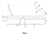
- Figure 1 illustrates a sectional view of a conventional gate bus-bar in a vertical field effect transistor (VFET).
- VFET vertical field effect transistor
- the substrate structure 10 of the VFET includes a semiconductor substrate 11 with a drift layer 12 formed thereon and a body layer 14 formed on the upper surface of layer 12.
- the substrate structure 10 is formed of doped semiconductor material so as to be electrically conductive.
- substrate 11 is a relatively heavily doped silicon (Si) substrate, in this case n+ Phosphourous doped (although other n-type of p-type dopants can be used)-.
- the drift layer 12 is a lighter n-type doped-Si .
- Body layer 14 is doped to the inverse polarity of the drift and substrate regions.
- a gate trench 16 extends downwardly through the body layer 14 into the drift layer 12 and is filled with polysilicon.
- the gate polysilicon (either stripes or other geometries) feed into the 'contact' gate trench.
- the gate polysilicon can extend out of the gate trench onto the silicon surface (but be separated physically from the Si by an insulating layer) with the metal contact being formed on the polysilicon residing on the silicon surface.
- an insulating TEOS layer 18 Provided on top of the substrate structure 10, covering the body layer 14 and the trench 16, is an insulating TEOS layer 18.
- a tungsten plug 20 extends through the TEOS layer 18 to provide an electrical contact to the polysilicon trench 16.
- a Ti and TiN barrier layer 22 is provided on top of the TEOS layer 18 and between the tungsten plug 20 and the polysilicon trench 16.
- An Aluminium (Al) contact layer 24 is provided on the barrier layer 22 and the tungsten plug 20 so as to provide a large electrical contact for tungsten plug 20.
- a passivating structure 26 covers the VFET and includes one or more layers which may include an oxide layer 28 with a SiN layer 30 formed thereon.
- VFET of Figure 1 has a gate bus-bar with a contact into a wide trench that the gate stripes connect into.
- Fig 1 illustrates the bus-bar and shows the wide trench that the fingers run into
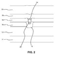
- FIG. 2 there is illustrated a sectional view of a VFET bus-bar according to an embodiment of the invention. It will be seen that the VFET of Figure 2 is similar to that of Figure 1 except that the aluminium contact layer 24 and the barrier layer 22 above the tungsten plug 20 has been removed (using an Al etching process to remove the aluminium 24 followed by a barrier etch to remove the barrier layer 22).
- the barrier etch is adapted to remove the TiN barrier layer 22.
- other barriers could be used and, in other embodiments, the W-Plug may not be planarised.
- the manufacturing process of the VFET of Figure 2 is similar to that of Figure 1 except that it comprises the additional step of removing the metal contact layer(s) provided above and in contact with the Tungsten plug contact 20.
- the resistivity of the Tungsten may be approximately 100 times smaller than that of the polysilicon gate trench 16.
- the resistivity of Tungsten at room temperature is approximately 5.6 ⁇ cm
- the resistivity of polysilicon may be in the range of 500-800 ⁇ cm (depending on factors such as the grain size, etc.).
- the Tungsten plug 20 may have a cross-sectional area that is around five times smaller (i.e. 20%) than that of the gate trench 16, resulting in the resistance of a stripe of tungsten plug being approximately twenty (20) times lower than that of the wide polysilicon gate trench 16.
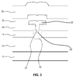
- a further improvement can be made by using a second barrier photolith prior to the Ti/TiNM/ barrier metal etch having previously left the W layer 32 unplanarised - this will protect the W plug and provide for an even lower resistance by allowing a Ti/TiNM/ region to extend from the contact hole onto the TEOS surface.
- the photolith process would leave some resist in place in the areas where the Al contact layer 24 and barrier layer 22 is desired to remain.
- the photomask is modified so that there is no resist left in the bus-bar area.
- the Al layer 24 is removed in the whole of the bus bar area and the Ti/TiN layer 22 and the W layer 32 remain everywhere. It will be understood, that if one was to then undertake an etch of the Ti/TiNM/ layers at this point, the barrier layers 22 and 32 would be removed to leave a structure like that of Figure 2 .
- a resist layer is placed where the barrier layers 22 and 32 are desired to remain (for example, in the same location as if making the structure of Figure 1 ), after barrier etching (and removing the photo resist) then we end up with fig 3 .
- the polysilicon of the gate may extend beyond the lateral extent of the gate trench.
- the plug may be adapted to contact the polysilicon outside of the gate trench (i.e. beyond the lateral extent of the gate terminal).
- the layer used to form the plug may extend beyond the lateral extent of the gate trench (which the poly being planarised).
- bus-bar construction of embodiments may be narrow, further improvements in Rg may be obtained by using many of these bus-bar structures in parallel with periodic trench interconnects between them.
- metal in the terms “source metal” and “gate metal” is not intended to exclude metallic, conductive arrangements that are not strictly speaking pure metal.
Landscapes
- Electrodes Of Semiconductors (AREA)
- Internal Circuitry In Semiconductor Integrated Circuit Devices (AREA)
Abstract
Description
- The invention relates to a semiconductor device having a gate trench and, more particularly, to a method of making the same.
- A gate finger refers to a single gate structure of a Field Effect Transistor (FET), and most FETs have multiple gate fingers or gate structures.
- The gate bus-bar is the electrical contact that is used to connect multiple gate structures or fingers together. A gate ring is a gate bus bar which extends around the outside of a semiconductor device and may form part of the edge termination of the device. Gate bus-bars may then be used to provide electrical contacts from the gate ring to the gates in the active area of the device.
- Gate resistance (Rg) is a parasitic element that affects the switching speed and uniformity of switching of a FET, and is inversely proportional to the cross-sectional area of conductor along the gate finger and proportional to the length of the finger.
- The addition of gate bus-bars is an effective way of reducing Rg but these structures increase active area usage and thus increase die area.
- There have been concerns over the reliability of bus-bars when a connection between the source metal and the package (for example a copper clip) is place over the bus-bar. One such concern has been that the gate bus-bar metal profile could contribute to cracking of the passivation layer increasing the probability of gate bus-bar short circuits.
- Removal of the gate bus-bar has been considered but this has been shown to significantly increase Rg and so is not practical. For example, in a design with a single central bus-bar, its removal would increase Rg by a factor of 3 to 4. Using a polysilicon only bus-bar also results in an unacceptably high Rg due to the high sheet resistance of polysilicon.
- According to the invention, there is provided a method of manufacturing a semiconductor device with a gate trench according to claim 1.
- Embodiments may provide an insulator topography that is flatter than conventional FETs and less susceptible to passivation layer cracking and/or shorting above the bus-bar. Also, the top electrical contact layer may be applied across the bus-bar with a reduced risk of cracking. This may be advantageous for devices having a small source clip that would otherwise prevent the use of a bus-bar without a continuous top contact layer covering the bus-bar.
- Thus, for semiconductor devices where it is not possible or practical to have a metal layer (such as an Aluminium metallisation layer) connecting to a bus-bar (or gate ring) due to area constraints or reliability concerns due to the use of a source connection clip, Rg can be improved by make use of a tungsten plug which contacts a gate trench of the device. This may be achieved using standard processing steps and may only require minor modification to device layout. Furthermore, such a concept may be employed for every gate stripe to significantly reduce gate resistance.
- For a better understanding of the invention, embodiments will now be described, purely by way of example, with reference to the accompanying drawings, in which:
-
Figure 1 shows a sectional view of the construction of a gate bus-bar in a conventional VFET where the bus-bar is contacting directly into the gate trench network; -
Figure 2 shows a sectional view of a VFET according to an embodiment of the invention; and -
Figure 3 shows a sectional view of a VFET according to another embodiment of the invention; and. - The same reference numbers are used for the same or corresponding features in the various figures and the description relating to these features is not necessarily repeated. The figures are schematic and not to scale.
- Proposed is the creation of a narrow flat polysilicon bus-bar with low resistance through the use of a tungsten-plug that is present in conventional FETs and a novel design.
-
Figure 1 illustrates a sectional view of a conventional gate bus-bar in a vertical field effect transistor (VFET). The manufacture of the VFET that would use the bus-bar construction ofFigure 1 is relatively standard and so will not be described in full detail. In particular, the formation of a VFET with a gate trench, body, source and drain is known. - The
substrate structure 10 of the VFET includes asemiconductor substrate 11 with adrift layer 12 formed thereon and abody layer 14 formed on the upper surface oflayer 12. Thesubstrate structure 10 is formed of doped semiconductor material so as to be electrically conductive. Here,substrate 11 is a relatively heavily doped silicon (Si) substrate, in this case n+ Phosphourous doped (although other n-type of p-type dopants can be used)-. Thedrift layer 12 is a lighter n-type doped-Si .Body layer 14 is doped to the inverse polarity of the drift and substrate regions. - A
gate trench 16 extends downwardly through thebody layer 14 into thedrift layer 12 and is filled with polysilicon. The gate polysilicon (either stripes or other geometries) feed into the 'contact' gate trench. Alternatively, the gate polysilicon can extend out of the gate trench onto the silicon surface (but be separated physically from the Si by an insulating layer) with the metal contact being formed on the polysilicon residing on the silicon surface. - Provided on top of the
substrate structure 10, covering thebody layer 14 and thetrench 16, is aninsulating TEOS layer 18. Atungsten plug 20 extends through the TEOSlayer 18 to provide an electrical contact to thepolysilicon trench 16. However, it is noted that a Ti andTiN barrier layer 22 is provided on top of the TEOSlayer 18 and between thetungsten plug 20 and thepolysilicon trench 16. - An Aluminium (Al)
contact layer 24 is provided on thebarrier layer 22 and thetungsten plug 20 so as to provide a large electrical contact fortungsten plug 20. Apassivating structure 26 covers the VFET and includes one or more layers which may include anoxide layer 28 with aSiN layer 30 formed thereon. - It will be understood that the VFET of
Figure 1 has a gate bus-bar with a contact into a wide trench that the gate stripes connect into. In other words,Fig 1 illustrates the bus-bar and shows the wide trench that the fingers run into - Turning now to
Figure 2 , there is illustrated a sectional view of a VFET bus-bar according to an embodiment of the invention. It will be seen that the VFET ofFigure 2 is similar to that ofFigure 1 except that thealuminium contact layer 24 and thebarrier layer 22 above thetungsten plug 20 has been removed (using an Al etching process to remove thealuminium 24 followed by a barrier etch to remove the barrier layer 22). - It will be appreciated that, in this example, the barrier etch is adapted to remove the
TiN barrier layer 22. However, other barriers could be used and, in other embodiments, the W-Plug may not be planarised. - It is noted that there may be some recessing of the
tungsten plug 20 due to erosion during the barrier etch. A layer of Aluminium may therefore be left in this recess covering thetungsten plug 20 but not the TEOS layer (as illustrated inFigure 2 ). However, it should also be noted that the Figures are not necessarily to scale. - Accordingly, the manufacturing process of the VFET of
Figure 2 is similar to that ofFigure 1 except that it comprises the additional step of removing the metal contact layer(s) provided above and in contact with the Tungstenplug contact 20. - The resistivity of the Tungsten may be approximately 100 times smaller than that of the
polysilicon gate trench 16. For example, the resistivity of Tungsten at room temperature is approximately 5.6 µΩcm, whilst the resistivity of polysilicon may be in the range of 500-800 µΩcm (depending on factors such as the grain size, etc.). In proposed embodiments, the Tungstenplug 20 may have a cross-sectional area that is around five times smaller (i.e. 20%) than that of thegate trench 16, resulting in the resistance of a stripe of tungsten plug being approximately twenty (20) times lower than that of the widepolysilicon gate trench 16. - A further improvement can be made by using a second barrier photolith prior to the Ti/TiNM/ barrier metal etch having previously left the
W layer 32 unplanarised - this will protect the W plug and provide for an even lower resistance by allowing a Ti/TiNM/ region to extend from the contact hole onto the TEOS surface. - For example, such an embodiment is shown in
Figure 3 . - In the conventional structure shown in
Figure 1 , prior to the Al etch, the photolith process would leave some resist in place in the areas where theAl contact layer 24 andbarrier layer 22 is desired to remain. In this further embodiment, however, the photomask is modified so that there is no resist left in the bus-bar area. In this way, after the Al etch, theAl layer 24 is removed in the whole of the bus bar area and the Ti/TiN layer 22 and theW layer 32 remain everywhere. It will be understood, that if one was to then undertake an etch of the Ti/TiNM/ layers at this point, thebarrier layers Figure 2 . - If however, before the barrier etch, a resist layer is placed where the
barrier layers Figure 1 ), after barrier etching (and removing the photo resist) then we end up withfig 3 . - It should be understood that, in alternative embodiments, the polysilicon of the gate may extend beyond the lateral extent of the gate trench. In such cases, the plug may be adapted to contact the polysilicon outside of the gate trench (i.e. beyond the lateral extent of the gate terminal). Thus, the layer used to form the plug may extend beyond the lateral extent of the gate trench (which the poly being planarised).
- It is noted that, because the bus-bar construction of embodiments may be narrow, further improvements in Rg may be obtained by using many of these bus-bar structures in parallel with periodic trench interconnects between them.
- This may also be extended to providing a plug into every trench stripe, therefore removing the need for metal bus-bars and providing very low Rg.
- It will be appreciated that available lithography and plug technology may, in practicality, set a limit on the minimum trench width that can be used, which may mean sacrificing cell pitch for low Rg. In this case, the processing may be more complex due to the need to isolate the poly plug from the source metal with a second dielectric deposition. This second dielectric layer may only be deposited with PECVD or a similar oxide as the maximum temperature should not exceed the point at which the TiN barrier layer under the tungsten plug is disrupted (short time at 450deg C).
- Those skilled in the art will realise that modifications are possible. For example, the term "metal" in the terms "source metal" and "gate metal" is not intended to exclude metallic, conductive arrangements that are not strictly speaking pure metal.
Claims (9)
- A method of manufacturing a semiconductor device having: a gate terminal formed from polysilicon and covered by an insulation layer; and a plug extending through an insulation layer to provide an electrical connection to the gate trench, the method comprising:depositing a metal layer which covers at least a portion of the insulation layer;
andetching the metal layer to remove the metal layer from above the plug. - The method of claim 1, wherein the gate terminal is formed within a gate trench and wherein the plug is formed from tungsten.
- The method of claim 1 or 2, further comprising the step of planarising the plug.
- The method of claim 2, wherein the plug contacts the gate terminal within the gate trench.
- The method of any preceding claim, wherein the polysilicon extends beyond the lateral extent of the gate terminal and wherein the plug contacts the polysilicon extending beyond the lateral extent of the gate terminal.
- The method of claim 2, further comprising the step of patterning the tungsten used to form the plug so that the plug extends beyond the beyond the lateral extent of the gate terminal.
- The method of any preceding claim, wherein the metal layer comprises aluminium and the step of etching comprises wet etching the metal layer.
- The method of any preceding claim, further comprising the step of forming a Ti-based barrier layer between the plug and the gate terminal.
- The method of any preceding claim, wherein the insulation layer is a TEOS layer.
Priority Applications (2)
| Application Number | Priority Date | Filing Date | Title |
|---|---|---|---|
| EP10178090.6A EP2432023B1 (en) | 2010-09-21 | 2010-09-21 | Method of manufacturing a trench gate semiconductor device |
| US13/237,878 US8652904B2 (en) | 2010-09-21 | 2011-09-20 | Semiconductor device with gate trench |
Applications Claiming Priority (1)
| Application Number | Priority Date | Filing Date | Title |
|---|---|---|---|
| EP10178090.6A EP2432023B1 (en) | 2010-09-21 | 2010-09-21 | Method of manufacturing a trench gate semiconductor device |
Publications (2)
| Publication Number | Publication Date |
|---|---|
| EP2432023A1 true EP2432023A1 (en) | 2012-03-21 |
| EP2432023B1 EP2432023B1 (en) | 2014-11-12 |
Family
ID=43629186
Family Applications (1)
| Application Number | Title | Priority Date | Filing Date |
|---|---|---|---|
| EP10178090.6A Active EP2432023B1 (en) | 2010-09-21 | 2010-09-21 | Method of manufacturing a trench gate semiconductor device |
Country Status (2)
| Country | Link |
|---|---|
| US (1) | US8652904B2 (en) |
| EP (1) | EP2432023B1 (en) |
Families Citing this family (1)
| Publication number | Priority date | Publication date | Assignee | Title |
|---|---|---|---|---|
| US9812538B2 (en) * | 2015-12-01 | 2017-11-07 | Infineon Technologies Americas Corp. | Buried bus and related method |
Citations (3)
| Publication number | Priority date | Publication date | Assignee | Title |
|---|---|---|---|---|
| US20040056302A1 (en) * | 2002-09-19 | 2004-03-25 | Grebs Thomas E. | Buried gate-field termination structure |
| US7049668B1 (en) * | 1998-08-25 | 2006-05-23 | Alpha And Omega Semiconductor, Ltd. | Gate contacting scheme of a trench MOSFET structure |
| US20100176445A1 (en) * | 2009-01-14 | 2010-07-15 | Force Mos Technology Co., Ltd. | Metal schemes of trench MOSFET for copper bonding |
Family Cites Families (6)
| Publication number | Priority date | Publication date | Assignee | Title |
|---|---|---|---|---|
| US7612407B2 (en) * | 2006-08-07 | 2009-11-03 | Force-Mos Technology Corp. Ltd | Trenched MOSFET device configuration with reduced mask processes |
| US8017982B2 (en) * | 2007-06-12 | 2011-09-13 | Micron Technology, Inc. | Imagers with contact plugs extending through the substrates thereof and imager fabrication methods |
| TW200903806A (en) * | 2007-07-11 | 2009-01-16 | Promos Technologies Inc | Power MOSFET structure and manufacturing method for the same |
| US8178922B2 (en) * | 2010-01-14 | 2012-05-15 | Force Mos Technology Co., Ltd. | Trench MOSFET with ultra high cell density and manufacture thereof |
| TWI438901B (en) * | 2010-05-27 | 2014-05-21 | Sinopower Semiconductor Inc | Power semiconductor component with low gate input resistance and manufacturing method thereof |
| US20120037954A1 (en) * | 2010-08-10 | 2012-02-16 | Force Mos Technology Co Ltd | Equal Potential Ring Structures of Power Semiconductor with Trenched Contact |
-
2010
- 2010-09-21 EP EP10178090.6A patent/EP2432023B1/en active Active
-
2011
- 2011-09-20 US US13/237,878 patent/US8652904B2/en active Active
Patent Citations (3)
| Publication number | Priority date | Publication date | Assignee | Title |
|---|---|---|---|---|
| US7049668B1 (en) * | 1998-08-25 | 2006-05-23 | Alpha And Omega Semiconductor, Ltd. | Gate contacting scheme of a trench MOSFET structure |
| US20040056302A1 (en) * | 2002-09-19 | 2004-03-25 | Grebs Thomas E. | Buried gate-field termination structure |
| US20100176445A1 (en) * | 2009-01-14 | 2010-07-15 | Force Mos Technology Co., Ltd. | Metal schemes of trench MOSFET for copper bonding |
Also Published As
| Publication number | Publication date |
|---|---|
| US8652904B2 (en) | 2014-02-18 |
| EP2432023B1 (en) | 2014-11-12 |
| US20120070983A1 (en) | 2012-03-22 |
Similar Documents
| Publication | Publication Date | Title |
|---|---|---|
| US9356022B2 (en) | Semiconductor device with termination structure for power MOSFET applications | |
| US11588040B2 (en) | LDMOS device and method for forming the same | |
| US9368621B1 (en) | Power semiconductor device having low on-state resistance | |
| US9911816B2 (en) | Semiconductive device and associated method of manufacture | |
| US8697520B2 (en) | Method of forming an asymmetric poly gate for optimum termination design in trench power MOSFETS | |
| US9123803B2 (en) | Semiconductor device and method for fabricating the same | |
| US20130134505A1 (en) | Semiconductor device for power and method of manufacture thereof | |
| US20150041962A1 (en) | Semiconductor Device with Cell Trench Structures and Contacts and Method of Manufacturing a Semiconductor Device | |
| EP1573824B1 (en) | Vertical insulated gate transistor and manufacturing method | |
| US9991378B2 (en) | Trench power semiconductor device | |
| US11996476B2 (en) | Methods and structures for contacting shield conductor in a semiconductor device | |
| US20170148889A1 (en) | Metal oxide semiconductor field effect transistor power device with multi gates connection | |
| US12543362B2 (en) | Contact field plate | |
| CN109638010B (en) | Radio frequency switching device and manufacturing method thereof | |
| EP2432023B1 (en) | Method of manufacturing a trench gate semiconductor device | |
| US20170062276A1 (en) | Semiconductor Device with Contact Structures Extending Through an Interlayer and Method of Manufacturing | |
| CN105702722B (en) | low on-resistance power semiconductor component | |
| US10008385B1 (en) | Enlarged sacrificial gate caps for forming self-aligned contacts | |
| EP3975246A1 (en) | Semiconductor die and method of manufacturing the same | |
| US20260129940A1 (en) | Contact field plate | |
| US20240194763A1 (en) | Hemt transistor | |
| US20070042553A1 (en) | Fabrication method for semiconductor memory components | |
| CN118039693A (en) | Semiconductor die and method of manufacturing a semiconductor die | |
| CN104241243A (en) | Semiconductor device structure and manufacturing method thereof | |
| HK1141137A (en) | Method of forming an mos transistor and structure therefor |
Legal Events
| Date | Code | Title | Description |
|---|---|---|---|
| PUAI | Public reference made under article 153(3) epc to a published international application that has entered the european phase |
Free format text: ORIGINAL CODE: 0009012 |
|
| AK | Designated contracting states |
Kind code of ref document: A1 Designated state(s): AL AT BE BG CH CY CZ DE DK EE ES FI FR GB GR HR HU IE IS IT LI LT LU LV MC MK MT NL NO PL PT RO SE SI SK SM TR |
|
| AX | Request for extension of the european patent |
Extension state: BA ME RS |
|
| 17P | Request for examination filed |
Effective date: 20120921 |
|
| RIC1 | Information provided on ipc code assigned before grant |
Ipc: H01L 29/423 20060101ALI20131217BHEP Ipc: H01L 29/49 20060101ALN20131217BHEP Ipc: H01L 21/336 20060101AFI20131217BHEP Ipc: H01L 29/78 20060101ALI20131217BHEP |
|
| REG | Reference to a national code |
Ref country code: DE Ref legal event code: R079 Ref document number: 602010020096 Country of ref document: DE Free format text: PREVIOUS MAIN CLASS: H01L0029780000 Ipc: H01L0021336000 |
|
| GRAP | Despatch of communication of intention to grant a patent |
Free format text: ORIGINAL CODE: EPIDOSNIGR1 |
|
| RIC1 | Information provided on ipc code assigned before grant |
Ipc: H01L 29/423 20060101ALI20140528BHEP Ipc: H01L 29/49 20060101ALN20140528BHEP Ipc: H01L 29/78 20060101ALI20140528BHEP Ipc: H01L 21/336 20060101AFI20140528BHEP |
|
| INTG | Intention to grant announced |
Effective date: 20140611 |
|
| GRAS | Grant fee paid |
Free format text: ORIGINAL CODE: EPIDOSNIGR3 |
|
| GRAA | (expected) grant |
Free format text: ORIGINAL CODE: 0009210 |
|
| AK | Designated contracting states |
Kind code of ref document: B1 Designated state(s): AL AT BE BG CH CY CZ DE DK EE ES FI FR GB GR HR HU IE IS IT LI LT LU LV MC MK MT NL NO PL PT RO SE SI SK SM TR |
|
| REG | Reference to a national code |
Ref country code: GB Ref legal event code: FG4D |
|
| REG | Reference to a national code |
Ref country code: CH Ref legal event code: EP |
|
| REG | Reference to a national code |
Ref country code: AT Ref legal event code: REF Ref document number: 696203 Country of ref document: AT Kind code of ref document: T Effective date: 20141115 |
|
| REG | Reference to a national code |
Ref country code: IE Ref legal event code: FG4D |
|
| REG | Reference to a national code |
Ref country code: DE Ref legal event code: R096 Ref document number: 602010020096 Country of ref document: DE Effective date: 20141224 |
|
| REG | Reference to a national code |
Ref country code: NL Ref legal event code: VDEP Effective date: 20141112 |
|
| REG | Reference to a national code |
Ref country code: AT Ref legal event code: MK05 Ref document number: 696203 Country of ref document: AT Kind code of ref document: T Effective date: 20141112 |
|
| PG25 | Lapsed in a contracting state [announced via postgrant information from national office to epo] |
Ref country code: PT Free format text: LAPSE BECAUSE OF FAILURE TO SUBMIT A TRANSLATION OF THE DESCRIPTION OR TO PAY THE FEE WITHIN THE PRESCRIBED TIME-LIMIT Effective date: 20150312 Ref country code: ES Free format text: LAPSE BECAUSE OF FAILURE TO SUBMIT A TRANSLATION OF THE DESCRIPTION OR TO PAY THE FEE WITHIN THE PRESCRIBED TIME-LIMIT Effective date: 20141112 Ref country code: LT Free format text: LAPSE BECAUSE OF FAILURE TO SUBMIT A TRANSLATION OF THE DESCRIPTION OR TO PAY THE FEE WITHIN THE PRESCRIBED TIME-LIMIT Effective date: 20141112 Ref country code: FI Free format text: LAPSE BECAUSE OF FAILURE TO SUBMIT A TRANSLATION OF THE DESCRIPTION OR TO PAY THE FEE WITHIN THE PRESCRIBED TIME-LIMIT Effective date: 20141112 Ref country code: NO Free format text: LAPSE BECAUSE OF FAILURE TO SUBMIT A TRANSLATION OF THE DESCRIPTION OR TO PAY THE FEE WITHIN THE PRESCRIBED TIME-LIMIT Effective date: 20150212 Ref country code: IS Free format text: LAPSE BECAUSE OF FAILURE TO SUBMIT A TRANSLATION OF THE DESCRIPTION OR TO PAY THE FEE WITHIN THE PRESCRIBED TIME-LIMIT Effective date: 20150312 Ref country code: NL Free format text: LAPSE BECAUSE OF FAILURE TO SUBMIT A TRANSLATION OF THE DESCRIPTION OR TO PAY THE FEE WITHIN THE PRESCRIBED TIME-LIMIT Effective date: 20141112 |
|
| PG25 | Lapsed in a contracting state [announced via postgrant information from national office to epo] |
Ref country code: SE Free format text: LAPSE BECAUSE OF FAILURE TO SUBMIT A TRANSLATION OF THE DESCRIPTION OR TO PAY THE FEE WITHIN THE PRESCRIBED TIME-LIMIT Effective date: 20141112 Ref country code: HR Free format text: LAPSE BECAUSE OF FAILURE TO SUBMIT A TRANSLATION OF THE DESCRIPTION OR TO PAY THE FEE WITHIN THE PRESCRIBED TIME-LIMIT Effective date: 20141112 Ref country code: CY Free format text: LAPSE BECAUSE OF FAILURE TO SUBMIT A TRANSLATION OF THE DESCRIPTION OR TO PAY THE FEE WITHIN THE PRESCRIBED TIME-LIMIT Effective date: 20141112 Ref country code: PL Free format text: LAPSE BECAUSE OF FAILURE TO SUBMIT A TRANSLATION OF THE DESCRIPTION OR TO PAY THE FEE WITHIN THE PRESCRIBED TIME-LIMIT Effective date: 20141112 Ref country code: GR Free format text: LAPSE BECAUSE OF FAILURE TO SUBMIT A TRANSLATION OF THE DESCRIPTION OR TO PAY THE FEE WITHIN THE PRESCRIBED TIME-LIMIT Effective date: 20150213 Ref country code: LV Free format text: LAPSE BECAUSE OF FAILURE TO SUBMIT A TRANSLATION OF THE DESCRIPTION OR TO PAY THE FEE WITHIN THE PRESCRIBED TIME-LIMIT Effective date: 20141112 Ref country code: AT Free format text: LAPSE BECAUSE OF FAILURE TO SUBMIT A TRANSLATION OF THE DESCRIPTION OR TO PAY THE FEE WITHIN THE PRESCRIBED TIME-LIMIT Effective date: 20141112 |
|
| PG25 | Lapsed in a contracting state [announced via postgrant information from national office to epo] |
Ref country code: CZ Free format text: LAPSE BECAUSE OF FAILURE TO SUBMIT A TRANSLATION OF THE DESCRIPTION OR TO PAY THE FEE WITHIN THE PRESCRIBED TIME-LIMIT Effective date: 20141112 Ref country code: SK Free format text: LAPSE BECAUSE OF FAILURE TO SUBMIT A TRANSLATION OF THE DESCRIPTION OR TO PAY THE FEE WITHIN THE PRESCRIBED TIME-LIMIT Effective date: 20141112 Ref country code: RO Free format text: LAPSE BECAUSE OF FAILURE TO SUBMIT A TRANSLATION OF THE DESCRIPTION OR TO PAY THE FEE WITHIN THE PRESCRIBED TIME-LIMIT Effective date: 20141112 Ref country code: DK Free format text: LAPSE BECAUSE OF FAILURE TO SUBMIT A TRANSLATION OF THE DESCRIPTION OR TO PAY THE FEE WITHIN THE PRESCRIBED TIME-LIMIT Effective date: 20141112 Ref country code: EE Free format text: LAPSE BECAUSE OF FAILURE TO SUBMIT A TRANSLATION OF THE DESCRIPTION OR TO PAY THE FEE WITHIN THE PRESCRIBED TIME-LIMIT Effective date: 20141112 |
|
| REG | Reference to a national code |
Ref country code: DE Ref legal event code: R097 Ref document number: 602010020096 Country of ref document: DE |
|
| REG | Reference to a national code |
Ref country code: FR Ref legal event code: PLFP Year of fee payment: 6 |
|
| PLBE | No opposition filed within time limit |
Free format text: ORIGINAL CODE: 0009261 |
|
| STAA | Information on the status of an ep patent application or granted ep patent |
Free format text: STATUS: NO OPPOSITION FILED WITHIN TIME LIMIT |
|
| 26N | No opposition filed |
Effective date: 20150813 |
|
| PG25 | Lapsed in a contracting state [announced via postgrant information from national office to epo] |
Ref country code: IT Free format text: LAPSE BECAUSE OF FAILURE TO SUBMIT A TRANSLATION OF THE DESCRIPTION OR TO PAY THE FEE WITHIN THE PRESCRIBED TIME-LIMIT Effective date: 20141112 |
|
| PG25 | Lapsed in a contracting state [announced via postgrant information from national office to epo] |
Ref country code: SI Free format text: LAPSE BECAUSE OF FAILURE TO SUBMIT A TRANSLATION OF THE DESCRIPTION OR TO PAY THE FEE WITHIN THE PRESCRIBED TIME-LIMIT Effective date: 20141112 |
|
| PG25 | Lapsed in a contracting state [announced via postgrant information from national office to epo] |
Ref country code: MC Free format text: LAPSE BECAUSE OF FAILURE TO SUBMIT A TRANSLATION OF THE DESCRIPTION OR TO PAY THE FEE WITHIN THE PRESCRIBED TIME-LIMIT Effective date: 20141112 Ref country code: LU Free format text: LAPSE BECAUSE OF FAILURE TO SUBMIT A TRANSLATION OF THE DESCRIPTION OR TO PAY THE FEE WITHIN THE PRESCRIBED TIME-LIMIT Effective date: 20150921 |
|
| REG | Reference to a national code |
Ref country code: CH Ref legal event code: PL |
|
| REG | Reference to a national code |
Ref country code: IE Ref legal event code: MM4A |
|
| PG25 | Lapsed in a contracting state [announced via postgrant information from national office to epo] |
Ref country code: LI Free format text: LAPSE BECAUSE OF NON-PAYMENT OF DUE FEES Effective date: 20150930 Ref country code: IE Free format text: LAPSE BECAUSE OF NON-PAYMENT OF DUE FEES Effective date: 20150921 Ref country code: CH Free format text: LAPSE BECAUSE OF NON-PAYMENT OF DUE FEES Effective date: 20150930 |
|
| REG | Reference to a national code |
Ref country code: FR Ref legal event code: PLFP Year of fee payment: 7 |
|
| REG | Reference to a national code |
Ref country code: DE Ref legal event code: R081 Ref document number: 602010020096 Country of ref document: DE Owner name: NEXPERIA B.V., NL Free format text: FORMER OWNER: NXP B.V., EINDHOVEN, NL |
|
| REG | Reference to a national code |
Ref country code: GB Ref legal event code: 732E Free format text: REGISTERED BETWEEN 20161013 AND 20161019 |
|
| REG | Reference to a national code |
Ref country code: FR Ref legal event code: TP Owner name: NEXPERIA B.V., NL Effective date: 20161109 |
|
| PG25 | Lapsed in a contracting state [announced via postgrant information from national office to epo] |
Ref country code: MT Free format text: LAPSE BECAUSE OF FAILURE TO SUBMIT A TRANSLATION OF THE DESCRIPTION OR TO PAY THE FEE WITHIN THE PRESCRIBED TIME-LIMIT Effective date: 20141112 |
|
| PG25 | Lapsed in a contracting state [announced via postgrant information from national office to epo] |
Ref country code: SM Free format text: LAPSE BECAUSE OF FAILURE TO SUBMIT A TRANSLATION OF THE DESCRIPTION OR TO PAY THE FEE WITHIN THE PRESCRIBED TIME-LIMIT Effective date: 20141112 Ref country code: BG Free format text: LAPSE BECAUSE OF FAILURE TO SUBMIT A TRANSLATION OF THE DESCRIPTION OR TO PAY THE FEE WITHIN THE PRESCRIBED TIME-LIMIT Effective date: 20141112 Ref country code: HU Free format text: LAPSE BECAUSE OF FAILURE TO SUBMIT A TRANSLATION OF THE DESCRIPTION OR TO PAY THE FEE WITHIN THE PRESCRIBED TIME-LIMIT; INVALID AB INITIO Effective date: 20100921 |
|
| PG25 | Lapsed in a contracting state [announced via postgrant information from national office to epo] |
Ref country code: TR Free format text: LAPSE BECAUSE OF FAILURE TO SUBMIT A TRANSLATION OF THE DESCRIPTION OR TO PAY THE FEE WITHIN THE PRESCRIBED TIME-LIMIT Effective date: 20141112 |
|
| REG | Reference to a national code |
Ref country code: FR Ref legal event code: PLFP Year of fee payment: 8 |
|
| PG25 | Lapsed in a contracting state [announced via postgrant information from national office to epo] |
Ref country code: BE Free format text: LAPSE BECAUSE OF FAILURE TO SUBMIT A TRANSLATION OF THE DESCRIPTION OR TO PAY THE FEE WITHIN THE PRESCRIBED TIME-LIMIT Effective date: 20141112 |
|
| PGFP | Annual fee paid to national office [announced via postgrant information from national office to epo] |
Ref country code: FR Payment date: 20170919 Year of fee payment: 8 Ref country code: GB Payment date: 20170928 Year of fee payment: 8 |
|
| PG25 | Lapsed in a contracting state [announced via postgrant information from national office to epo] |
Ref country code: MK Free format text: LAPSE BECAUSE OF FAILURE TO SUBMIT A TRANSLATION OF THE DESCRIPTION OR TO PAY THE FEE WITHIN THE PRESCRIBED TIME-LIMIT Effective date: 20141112 |
|
| PG25 | Lapsed in a contracting state [announced via postgrant information from national office to epo] |
Ref country code: AL Free format text: LAPSE BECAUSE OF FAILURE TO SUBMIT A TRANSLATION OF THE DESCRIPTION OR TO PAY THE FEE WITHIN THE PRESCRIBED TIME-LIMIT Effective date: 20141112 |
|
| GBPC | Gb: european patent ceased through non-payment of renewal fee |
Effective date: 20180921 |
|
| PG25 | Lapsed in a contracting state [announced via postgrant information from national office to epo] |
Ref country code: FR Free format text: LAPSE BECAUSE OF NON-PAYMENT OF DUE FEES Effective date: 20180930 |
|
| PG25 | Lapsed in a contracting state [announced via postgrant information from national office to epo] |
Ref country code: GB Free format text: LAPSE BECAUSE OF NON-PAYMENT OF DUE FEES Effective date: 20180921 |
|
| REG | Reference to a national code |
Ref country code: DE Ref legal event code: R079 Ref document number: 602010020096 Country of ref document: DE Free format text: PREVIOUS MAIN CLASS: H01L0021336000 Ipc: H10D0030010000 |
|
| PGFP | Annual fee paid to national office [announced via postgrant information from national office to epo] |
Ref country code: DE Payment date: 20250926 Year of fee payment: 16 |