EP2426136A1 - Growth of Al2O3 thin films from trialkyllaluminum for photovoltaic applications - Google Patents
Growth of Al2O3 thin films from trialkyllaluminum for photovoltaic applications Download PDFInfo
- Publication number
- EP2426136A1 EP2426136A1 EP10305955A EP10305955A EP2426136A1 EP 2426136 A1 EP2426136 A1 EP 2426136A1 EP 10305955 A EP10305955 A EP 10305955A EP 10305955 A EP10305955 A EP 10305955A EP 2426136 A1 EP2426136 A1 EP 2426136A1
- Authority
- EP
- European Patent Office
- Prior art keywords
- ppb
- ppm
- deposition
- composition
- film
- Prior art date
- Legal status (The legal status is an assumption and is not a legal conclusion. Google has not performed a legal analysis and makes no representation as to the accuracy of the status listed.)
- Granted
Links
Images


Classifications
-
- C—CHEMISTRY; METALLURGY
- C23—COATING METALLIC MATERIAL; COATING MATERIAL WITH METALLIC MATERIAL; CHEMICAL SURFACE TREATMENT; DIFFUSION TREATMENT OF METALLIC MATERIAL; COATING BY VACUUM EVAPORATION, BY SPUTTERING, BY ION IMPLANTATION OR BY CHEMICAL VAPOUR DEPOSITION, IN GENERAL; INHIBITING CORROSION OF METALLIC MATERIAL OR INCRUSTATION IN GENERAL
- C23C—COATING METALLIC MATERIAL; COATING MATERIAL WITH METALLIC MATERIAL; SURFACE TREATMENT OF METALLIC MATERIAL BY DIFFUSION INTO THE SURFACE, BY CHEMICAL CONVERSION OR SUBSTITUTION; COATING BY VACUUM EVAPORATION, BY SPUTTERING, BY ION IMPLANTATION OR BY CHEMICAL VAPOUR DEPOSITION, IN GENERAL
- C23C16/00—Chemical coating by decomposition of gaseous compounds, without leaving reaction products of surface material in the coating, i.e. chemical vapour deposition [CVD] processes
- C23C16/44—Chemical coating by decomposition of gaseous compounds, without leaving reaction products of surface material in the coating, i.e. chemical vapour deposition [CVD] processes characterised by the method of coating
- C23C16/455—Chemical coating by decomposition of gaseous compounds, without leaving reaction products of surface material in the coating, i.e. chemical vapour deposition [CVD] processes characterised by the method of coating characterised by the method used for introducing gases into reaction chamber or for modifying gas flows in reaction chamber
- C23C16/45523—Pulsed gas flow or change of composition over time
- C23C16/45525—Atomic layer deposition [ALD]
- C23C16/45553—Atomic layer deposition [ALD] characterized by the use of precursors specially adapted for ALD
-
- H—ELECTRICITY
- H10—SEMICONDUCTOR DEVICES; ELECTRIC SOLID-STATE DEVICES NOT OTHERWISE PROVIDED FOR
- H10F—INORGANIC SEMICONDUCTOR DEVICES SENSITIVE TO INFRARED RADIATION, LIGHT, ELECTROMAGNETIC RADIATION OF SHORTER WAVELENGTH OR CORPUSCULAR RADIATION
- H10F77/00—Constructional details of devices covered by this subclass
- H10F77/30—Coatings
- H10F77/306—Coatings for devices having potential barriers
- H10F77/311—Coatings for devices having potential barriers for photovoltaic cells
-
- Y—GENERAL TAGGING OF NEW TECHNOLOGICAL DEVELOPMENTS; GENERAL TAGGING OF CROSS-SECTIONAL TECHNOLOGIES SPANNING OVER SEVERAL SECTIONS OF THE IPC; TECHNICAL SUBJECTS COVERED BY FORMER USPC CROSS-REFERENCE ART COLLECTIONS [XRACs] AND DIGESTS
- Y02—TECHNOLOGIES OR APPLICATIONS FOR MITIGATION OR ADAPTATION AGAINST CLIMATE CHANGE
- Y02E—REDUCTION OF GREENHOUSE GAS [GHG] EMISSIONS, RELATED TO ENERGY GENERATION, TRANSMISSION OR DISTRIBUTION
- Y02E10/00—Energy generation through renewable energy sources
- Y02E10/50—Photovoltaic [PV] energy
Definitions
- the present invention concerns a composition of Trialkylaluminium containing metal impurities, useful for the deposition of thin films in photovoltaic technologies, in particular for solar cells.
- the photovoltaic effect is known since the end of the 19 th century.
- the principle consists in converting light energy into electricity. In the current ecological context, this is a promising solution to produce clean and renewable energy.
- One of the reasons for the slow development of photovoltaic electricity up to now is its lack of competitiveness compared to the traditional solutions such as coal, fossil fuels or nuclear based electricity. So the contribution of solar electricity as one significant component of the future energy mix is bounded to the capability to continue the cost per watt peak reduction race. To reach this goal, reduction of the manufacturing costs and improvement of cell's efficiency are two solutions.
- Figure 1 and Figure 2 detail conversion efficiency of p-type and n-type wafers based solar cells depending on concentration of selected metallic impurities.
- Iron will also form an oxide, when oxygen is present in the bulk. This oxide is an additional defect in the structure and then a recombination center.
- Titanium and molybdenum will diffuse slowly into the bulk and form active recombination centers after high temperature firing.
- transition metals more precisely iron, copper, tantalum or molybdenum, are particularly detrimental to the global performance of solar cells ( A.A. Istratov, C. Flink, H. Hieslmair, S.A. McHugo, E.R. Weber; "Diffusion, solubility and gettring of copper in silicon”; Materials Science and engineering B72 (2000) 99-104 ).
- impurities can be introduced during the wafer processing itself or during handling.
- contamination can result from usage of inappropriate grade chemicals.
- CVD process for example, these undesirable elements will be transferred in the gas phase with the main compounds and then incorporated into the layers to be deposited, more precisely, in the passivation layers.
- Al 2 O 3 deposition - for surface of silicon wafer based solar cells - performed by ALD, i.e Atomic Layer Deposition, or MOCVD, i.e Metal-Organic Chemical Vapor Deposition ( Agostinelli et al. "Very Low surface recombination velocities on p-type silicon wafers passivated with a dielectric with fixed negative charge”; Solar Energy Materials & Solar Cells, 90 (2006), 3438-3443 ), or PECVD, i.e.
- Plasma Enhanced Chemical Vapor Phase Deposition (Saint- Cast et al., Very low surface recombination velocity on p-type c-Si by high-rate plasma-deposited aluminum oxide, APPLIED PHYSICS LETTERS 95, 151502 _2009 ) or any other vapor-phase deposition technique can induce incorporation of impurities in the deposited layer, these impurities are to be found originally in the aluminium source precursor, usually trimethylaluminum (TMA), but alternatively a trialkylaluminum such as triethylaluminum (TEA), used for such deposition processes.
- TMA trimethylaluminum
- TAA triethylaluminum
- Table 1 details typical impurity upper limits concentrations and requirements for trimethylaluminum precursor to be used in the electronics industry (for example, MOCVD of epitaxial AlGaAs, AlGaN and InAlGaP films for applications in products such as high brightness LEDs and lasers and more recently ALD of aluminium oxide, which is the dielectric layer of choice in DRAM devices). These limits are based on process chemical guidelines (SEMI C66-0308 - Guidelines for Trimethylaluminium (TMAI), 99.5% Quality) approved by the global Liquid Chemicals Committee and available since February 2008. These guidelines give appropriate metal and general contamination information to assist end users and chemical manufacturers.
- TMAI Trimethylaluminium
- the TMA precursor does not meet the requirements for usage in the manufacturing of a semiconductor.
- the grad as defined in table 1 is named "semiconductor grade" in the present description.
- Table 1 Typical impurities concentration in semiconductor grade trimethylaluminum precursor Semiconductor grade (ppbw) B Boron B Ca Calcium Ca Cr Chromium Cr Cu Copper Cu Fe Iron Fe K Potassium K Na Sodium Na Ni Nickel Ni Zn Zinc Zn Ti Titanium Ti Mn Manganese Mn Co Cobalt Co
- a "non-semiconductor grade" TMA usage for deposition of Al 2 O 3 surface passivation layer could be a non-negligible source of contamination with strong lifetime killers such as iron or copper.
- Al 2 O 3 is used in the semiconductor industry for several applications such as passivation and electrical insulation.
- semiconductor grade aluminum precursor is commonly used to avoid any metallic impurities potentially generating undesirable phenomena such as leakage currents.
- non-semiconductor grade aluminum precursor can be used for deposition of a surface passivation layer in crystalline silicon wafer based solar cells manufacturing as such non-semiconductor grade chemical usage does not induce any observable deterioration of the cell's performance (evaluated for example with the measurement of the lifetime carrier).
- Another application of the non-semiconductor grade trialkylaluminum could be the deposition of Al 2 O 3 for encapsulation of photovoltaic devices.
- the present invention concerns a composition
- a composition comprising, for 100% of its total mass, at least 97% of a Trialkylaluminium and:
- composition as defined above comprises also:
- the composition as defined above comprises other metal impurities such as B (Boron), Ca (Calcium), K (Potassium), Cr (Chromium), Na (Sodium), Nb (Niobium), Ti (Titanium), Mn (Manganese), Co (Cobalt), Sn (Tin) in a quantity comprised between 0 and 20ppm for each of them.
- metal impurities such as B (Boron), Ca (Calcium), K (Potassium), Cr (Chromium), Na (Sodium), Nb (Niobium), Ti (Titanium), Mn (Manganese), Co (Cobalt), Sn (Tin) in a quantity comprised between 0 and 20ppm for each of them.
- the Trialkylaluminium is selected from Trimethylaluminum and Triethylaluminum.
- the invention concerns the use of a composition as defined above for a thin film deposition method by ALD, PEALD, CVD, PECVD or MOCVD.
- the invention concerns the use as defined above, wherein the deposition method is an ALD method.
- the invention concerns the use as defined above wherein the thin film is a film of Al 2 O 3 .
- the invention concerns the use as defined above for Al 2 O 3 growth for photovoltaic applications.
- the invention concerns the use as defined above wherein the composition as defined above comprises from 97% to 99,4% of Trialkylaluminium selected from Trimethylaluminum and Triethylaluminum.
- the invention concerns a film of Al 2 O 3 obtained by the use as defined above.
- the invention concerns the use of the film as defined above for the passivation of photovoltaic devices, in particular for solar cells.
- the invention concerns the use of the film as defined above for the encapsulation of photovoltaic devices, in particular for solar cells.
- This chemical with such grade has the advantages of allowing deposition of Al 2 O 3 layers for passivation by ALD, MOCVD, PECVD or any other derivative deposition methods without observable degradation of the performance of the solar cell (evaluated with minority carrier lifetime measurements). Furthermore, for encapsulation purposes, ALD or any other derivative deposition methods can be considered to fabricate an Al 2 O 3 film from such "non-semiconductor grade" chemicals.
- This novel intermediate grade precursor's usage is not solely limited to the deposition of a surface passivation layer for crystalline silicon wafer based photovoltaic solar cell but its benefit could be applied to other manufacturing steps in the photovoltaic industry such as encapsulation process. As well, such lower grade aluminium precursors could be used in various other application fields.
- the vaporization of the new precursor "non-semiconductor grade" can be performed by introducing a gas in a canister containing the said trialkylaluminum "non-semiconductor grade” source.
- the canister is preferably heated at a temperature which allows to vaporize the said source with a sufficient vapor pressure.
- the carrier gas can be selected from Ar, He, H 2 , N 2 or mixtures of them.
- the canister can for instance be heated at temperatures in the range of 15°C to 170°C. The temperature can be adjusted to control the amount of precursor in the gas phase.
- the said trialkylaluminum "non-semiconductor grade" source is fed in the liquid state to a vaporizer where it is vaporized.
- the pressure in the said canister is in the range from 133 mPa to 133.10 2 Pa.
- the said vaporized metal source is introduced into a reaction chamber where it is contacted to a solar cell substrate.
- the substrate can be covered with a material from the group Si, SiO 2 , SiN, SiON, and other silicon containing substrates and films and even other metal containing films.
- the substrate can be heated to sufficient temperature to obtain the desired film at sufficient growth rate and with desired physical state and composition. Typical temperature range from room temperature to 600°C and preferably from 150°C to 600°C. Preferably the temperature is lower or equal to 450°C.
- the pressure in the reaction chamber is controlled to obtain the desired metal containing film at sufficient growth rate. The typical pressures range from 133 mPa to 133.10 2 Pa or higher.
- the said trialkylaluminum "non-semiconductor grade" source described above is mixed to one or more reactant species prior to the reaction chamber.
- the said trialkylaluminum "non-semiconductor grade" source described above is mixed to one or more reactant species in the reaction chamber.
- the said trialkylaluminum non semiconductor grade source and the reactant species are introduced sequentially in the reaction chamber.
- the trialkylaluminum "non-semiconductor grade” source and the reactant species can be introduced simultaneously (chemical vapor deposition), sequentially (atomic layer deposition) or different combinations (one example is to introduce the reactant species (one example could be oxygen) continuously and to introduce trialkylaluminum "non-semiconductor grade” source by pulse (pulsed-chemical vapor deposition).
- the reactant species are decomposed into radicals in a plasma system prior to entering in the reaction chamber.
- the said reactant species include an oxygen source which is selected from oxygen (O 2 ), oxygen-containing radicals (for instance O ⁇ or OH ⁇ ), for instance generated by an oxygen (O 2 ), carbon dioxide (CO 2 ) or nitrogen dioxide (NO 2 ) plasma, ozone (O 3 ), moisture (H 2 O) and H 2 O 2 .
- oxygen source which is selected from oxygen (O 2 ), oxygen-containing radicals (for instance O ⁇ or OH ⁇ ), for instance generated by an oxygen (O 2 ), carbon dioxide (CO 2 ) or nitrogen dioxide (NO 2 ) plasma, ozone (O 3 ), moisture (H 2 O) and H 2 O 2 .
- the said trialkylaluminum "non-semiconductor grade" source is used for atomic layer deposition of Al 2 O 3 films.
- the said aluminum source and the reactant species are introduced sequentially in the reaction chamber (atomic layer deposition).
- the reactor pressure is selected in the range from 133 mPa to 133.10 2 Pa. Preferably the reactor pressure is comprised between 133 Pa and 1330 Pa.
- a purge gas is introduced between the metal source pulse and the reactant species pulse.
- the purge gas can be selected without limitation from the group consisting of N 2 , Ar, He.
- the aluminum source, purge gas and reactant species pulse duration is comprised between 1ms and 10 seconds. The pulse duration is preferably about 10 ms.
Landscapes
- Chemical & Material Sciences (AREA)
- General Chemical & Material Sciences (AREA)
- Chemical Kinetics & Catalysis (AREA)
- Engineering & Computer Science (AREA)
- Materials Engineering (AREA)
- Mechanical Engineering (AREA)
- Metallurgy (AREA)
- Organic Chemistry (AREA)
- Photovoltaic Devices (AREA)
- Chemical Vapour Deposition (AREA)
Abstract
- From 200 ppb to 5 ppm of Mo (Molybdenum);
- From 1000 ppb to 5 ppm of Fe (Iron);
- From 200 ppb to 5 ppm of Cu (Copper);
- From 200 ppb to 10 ppm of Ta (Tantalum).
Description
- The present invention concerns a composition of Trialkylaluminium containing metal impurities, useful for the deposition of thin films in photovoltaic technologies, in particular for solar cells.
- The photovoltaic effect is known since the end of the 19th century. The principle consists in converting light energy into electricity. In the current ecological context, this is a promising solution to produce clean and renewable energy. One of the reasons for the slow development of photovoltaic electricity up to now is its lack of competitiveness compared to the traditional solutions such as coal, fossil fuels or nuclear based electricity. So the contribution of solar electricity as one significant component of the future energy mix is bounded to the capability to continue the cost per watt peak reduction race. To reach this goal, reduction of the manufacturing costs and improvement of cell's efficiency are two solutions.
- Reduction of the manufacturing costs is addressed for example with thinner wafers usage to limit the impact of silicon feedstock price on the overall cell's cost (in 2010, cost split is 55 % for wafer - with 23 % for silicon feedstock, 13 % for silicon growth and 18 % for wafering step - and 45 % for cell processing), and in general with reduced raw materials consumption, including chemicals used during each step of the manufacturing. This manufacturing cost decrease is driven by manufacturing tools providers (the OEM - Original Equipment Manufacturers) and by material suppliers.
- Improvement of photovoltaic cell's efficiency requires innovation activity that takes place in the Research laboratories. The passivation phenomenon related work carried out by academics may contribute to the enhancement of the photovoltaic cell's performance. Passivation of the cell's defects by for example hydrogen increases the efficiency of the cell by reducing the probability of holeelectron pairs' recombination at the surface and in the bulk of the silicon: the lower the number of defects into the material the higher the probability that charge carriers are collected. These recombinations take place on the front side of the solar cell as well as on the backside. To prevent the backside recombination, the deposition of a thin Al2O3 layer has been described in the literature (for example P.Vitanov and al. "Chemical Deposition of Al2O3 thin films on Si substrates" Thin Solid Films, 517 (2009), 6327-6330) as well as Hoex et al. "Silicon surface passivation by atomic layer deposited Al2O3" JOURNAL OF APPLIED PHYSICS 104, 044903 2008_demonstrated that very thin ALD- Al2O3 layers (5-30 nm) can provide an excellent surface passivation for n-type and p-type silicon wafers after annealing at 425°C. This layer contributes to passivation in two ways: reduction of interface defects density and field-effect passivation thanks to high negative charge density at the silicon - alumina interface (G. Dingemans, R. Seguin, P. Engelhart, M.C.M. van de Sanden and W.M.M. Kessels; "silicon surface passivation by ultrathin Al2O3 films synthesized by thermal and plasma atomic layer deposition"; Phys. Status Solidi RRL4, N° 1-2, 10-12 (2010)).
- Recombination also occurs in the bulk of the silicon. Therefore, for an effective collection of the carriers, their diffusion length (average distance covered by a charge carrier before it gets recombined) or lifetime should be at least equal to the wafer thickness (V.G. Litovchenko, N.I. Klyuis, A.A. Evtukh, A.A. Efremov, A.V. Sarikov, et al.; "Solar cells prepared on multicrystalline silicon subjected to new gettering and passivation treatments"; Solar Energy Materials and Solar Cells, 72 (2002), 343-351). Injection of atomic hydrogen to passivate the defects and reduction of the amount of metallic impurities into the bulk are two major solutions to increase diffusion length. Several sources of contamination can be identified during the different manufacturing steps: from the silicon wafer production, including the silicon ingot or silicon casting steps, to the solar cell fabrication where lots of chemicals are used. The detrimental impact of some impurities such as copper or iron on the lifetime of charge carriers is known thanks to studies carried out for the semiconductor industry.
Figure 1 andFigure 2 detail conversion efficiency of p-type and n-type wafers based solar cells depending on concentration of selected metallic impurities. -
Figure 1 shows the effect of metal impurity concentration on p-type Cz-Si based solar cells' conversion efficiency. -
Figure 2 shows the effect of metal impurity concentration on n-type Cz-Si based solar cells' conversion efficiency. - The detrimental effect of iron in a boron doped (p-type) silicon wafer is described by Zoth et al ("Silicon contamination control by lifetime measurements"; in Analytical and Diagnostic Techniques for Semiconductor Materials, Devices and Processes (eds. Kolbesen et al.), The Electrochemical Society proceedings, volume ECS PV 99-16 (1999)). During the high temperature firing step (about 800°C) required by most solar cell manufacturing processes, iron atoms, also those possibly and unintentionally deposited with the Al2O3, will be scattered uniformly into the silicon bulk due to diffusion phenomena. These atoms will be located on interstitial sites and some of them will combine reversibly with a boron atom. Injection of minority carrier in silicon by photo excitation will dissociate the FeB pairs and therefore interstitial iron atoms will become recombination centers which are ten times stronger than FeB.
- Iron will also form an oxide, when oxygen is present in the bulk. This oxide is an additional defect in the structure and then a recombination center.
- Other metallic impurities such as copper and nickel will have an impact on the surface of the wafer where they will precipitate and form recombination centers. Titanium and molybdenum will diffuse slowly into the bulk and form active recombination centers after high temperature firing.
- To conclude, experts of silicon science consider that transition metals, more precisely iron, copper, tantalum or molybdenum, are particularly detrimental to the global performance of solar cells (A.A. Istratov, C. Flink, H. Hieslmair, S.A. McHugo, E.R. Weber; "Diffusion, solubility and gettring of copper in silicon"; Materials Science and engineering B72 (2000) 99-104).
- It is easily understood that impurities can be introduced during the wafer processing itself or during handling. During solar cells' manufacturing, contamination can result from usage of inappropriate grade chemicals. In a CVD process for example, these undesirable elements will be transferred in the gas phase with the main compounds and then incorporated into the layers to be deposited, more precisely, in the passivation layers.
- Based on the above information resulting from extensive experience of the scientific community, it is obvious that Al2O3 deposition - for surface of silicon wafer based solar cells - performed by ALD, i.e Atomic Layer Deposition, or MOCVD, i.e Metal-Organic Chemical Vapor Deposition (Agostinelli et al. "Very Low surface recombination velocities on p-type silicon wafers passivated with a dielectric with fixed negative charge"; Solar Energy Materials & Solar Cells, 90 (2006), 3438-3443), or PECVD, i.e. Plasma Enhanced Chemical Vapor Phase Deposition (Saint-Cast et al., Very low surface recombination velocity on p-type c-Si by high-rate plasma-deposited aluminum oxide, APPLIED PHYSICS LETTERS 95, 151502 _2009) or any other vapor-phase deposition technique can induce incorporation of impurities in the deposited layer, these impurities are to be found originally in the aluminium source precursor, usually trimethylaluminum (TMA), but alternatively a trialkylaluminum such as triethylaluminum (TEA), used for such deposition processes. One could argue that the impurities would be segregated into the passivation alumina layer but this consideration does not take into account that each metallic impurity has a specific diffusion factor and that this diffusion phenomenon from the alumina layer to the silicon bulk increases with temperature. Therefore, the more contaminated the passivation layer, the more contaminated the silicon due to enhancement of diffusion during the mandatory annealing or other high temperature steps (see
Figure 3 ). - Table 1 details typical impurity upper limits concentrations and requirements for trimethylaluminum precursor to be used in the electronics industry (for example, MOCVD of epitaxial AlGaAs, AlGaN and InAlGaP films for applications in products such as high brightness LEDs and lasers and more recently ALD of aluminium oxide, which is the dielectric layer of choice in DRAM devices). These limits are based on process chemical guidelines (SEMI C66-0308 - Guidelines for Trimethylaluminium (TMAI), 99.5% Quality) approved by the global Liquid Chemicals Committee and available since February 2008. These guidelines give appropriate metal and general contamination information to assist end users and chemical manufacturers. If the quantity of one of the impurities is superior to the present limit, the TMA precursor does not meet the requirements for usage in the manufacturing of a semiconductor. The grad as defined in table 1 is named "semiconductor grade" in the present description.
Table 1: Typical impurities concentration in semiconductor grade trimethylaluminum precursor Semiconductor grade
(ppbw)B Boron B Ca Calcium Ca Cr Chromium Cr Cu Copper Cu Fe Iron Fe K Potassium K Na Sodium Na Ni Nickel Ni Zn Zinc Zn Ti Titanium Ti Mn Manganese Mn Co Cobalt Co - Data of Table 1 and the above discussion encourage a solar cell manufacturer to use "semiconductor grade" TMA to avoid any risk of contamination and therefore any possible degradation of the cells' efficiency: A "non-semiconductor grade" TMA usage for deposition of Al2O3 surface passivation layer could be a non-negligible source of contamination with strong lifetime killers such as iron or copper.
- Al2O3 is used in the semiconductor industry for several applications such as passivation and electrical insulation. For these applications, "semiconductor grade" aluminum precursor is commonly used to avoid any metallic impurities potentially generating undesirable phenomena such as leakage currents.
- Nevertheless, the inventors of the present invention show that astonishingly the usage of a non-semiconductor grade aluminum precursor can be used for deposition of a surface passivation layer in crystalline silicon wafer based solar cells manufacturing as such non-semiconductor grade chemical usage does not induce any observable deterioration of the cell's performance (evaluated for example with the measurement of the lifetime carrier). Another application of the non-semiconductor grade trialkylaluminum could be the deposition of Al2O3 for encapsulation of photovoltaic devices.
- The present invention concerns a composition comprising, for 100% of its total mass, at least 97% of a Trialkylaluminium and:
- From 200 ppb to 5 ppm of Mo (Molybdenum);
- From 1000 ppb to 5 ppm of Fe (Iron);
- From 200 ppb to 5 ppm of Cu (Copper);
- From 200 ppb to 10 ppm of Ta (Tantalum).
- According one embodiment of the invention, the composition as defined above comprises also:
- From 5000 ppb to 10 ppm of Ni (Nickel);
- From 2000 ppb to 10 ppm of Zn (Zinc);
- From 5000 ppb to 10 ppm of W (Tungsten).
- According another embodiment of the invention the composition as defined above comprises other metal impurities such as B (Boron), Ca (Calcium), K (Potassium), Cr (Chromium), Na (Sodium), Nb (Niobium), Ti (Titanium), Mn (Manganese), Co (Cobalt), Sn (Tin) in a quantity comprised between 0 and 20ppm for each of them.
- According another embodiment of the invention, the Trialkylaluminium is selected from Trimethylaluminum and Triethylaluminum.
- According another embodiment, the invention concerns the use of a composition as defined above for a thin film deposition method by ALD, PEALD, CVD, PECVD or MOCVD.
- According another embodiment, the invention concerns the use as defined above, wherein the deposition method is an ALD method.
- According another embodiment, the invention concerns the use as defined above wherein the thin film is a film of Al2O3.
- According another embodiment, the invention concerns the use as defined above for Al2O3 growth for photovoltaic applications.
- According another embodiment, the invention concerns the use as defined above wherein the composition as defined above comprises from 97% to 99,4% of Trialkylaluminium selected from Trimethylaluminum and Triethylaluminum.
- According another embodiment, the invention concerns a film of Al2O3 obtained by the use as defined above.
- According another embodiment, the invention concerns the use of the film as defined above for the passivation of photovoltaic devices, in particular for solar cells.
- According another embodiment, the invention concerns the use of the film as defined above for the encapsulation of photovoltaic devices, in particular for solar cells.
- From the background of the invention, the inventors understood that a "semiconductor grade" aluminum precursor was mandatory for specific applications but they have concluded that surprisingly a "non semiconductor grade" trialkylaluminum can be used for the purpose of depositing a surface passivation alumina layer for crystalline silicon wafer based photovoltaic solar cell. Actually, the examples detailed below show that contrary to what was expected, usage of "non semiconductor grade" aluminum precursor (chemical with enlarged tolerance on the amount of impurities than "semiconductor grade" one) is a suitable technical solution to achieve performance meeting the photovoltaic solar cells' expectations. Also for any photovoltaic devices, encapsulation issues can be addressed by Atomic Layer Deposition or any other suitable vapor phase deposition technique of Al2O3 deposited with "non-semiconductor" grade trialkylaluminum.
- This chemical with such grade has the advantages of allowing deposition of Al2O3 layers for passivation by ALD, MOCVD, PECVD or any other derivative deposition methods without observable degradation of the performance of the solar cell (evaluated with minority carrier lifetime measurements). Furthermore, for encapsulation purposes, ALD or any other derivative deposition methods can be considered to fabricate an Al2O3 film from such "non-semiconductor grade" chemicals.
- This novel intermediate grade precursor's usage is not solely limited to the deposition of a surface passivation layer for crystalline silicon wafer based photovoltaic solar cell but its benefit could be applied to other manufacturing steps in the photovoltaic industry such as encapsulation process. As well, such lower grade aluminium precursors could be used in various other application fields.
- The deposition of an Al2O3 thin film requires several steps:
- a. Vaporizing the trialkylaluminum source to form an aluminum source gas phase.
- b. Introducing several precursors in vapor phase in a deposition device, wherein said precursors comprise said vaporized trialkylaluminum source, and oxygen source without limitation oxygen, carbon dioxide or nitrogen dioxide plasma, ozone, oxygen, water.
- In one embodiment of the invention, the vaporization of the new precursor "non-semiconductor grade" can be performed by introducing a gas in a canister containing the said trialkylaluminum "non-semiconductor grade" source. The canister is preferably heated at a temperature which allows to vaporize the said source with a sufficient vapor pressure. The carrier gas can be selected from Ar, He, H2, N2 or mixtures of them. The canister can for instance be heated at temperatures in the range of 15°C to 170°C. The temperature can be adjusted to control the amount of precursor in the gas phase.
- In another embodiment of the invention, the said trialkylaluminum "non-semiconductor grade" source is fed in the liquid state to a vaporizer where it is vaporized.
- In one embodiment of the invention, the pressure in the said canister is in the range from 133 mPa to 133.102 Pa.
- The said vaporized metal source is introduced into a reaction chamber where it is contacted to a solar cell substrate. The substrate can be covered with a material from the group Si, SiO2, SiN, SiON, and other silicon containing substrates and films and even other metal containing films. The substrate can be heated to sufficient temperature to obtain the desired film at sufficient growth rate and with desired physical state and composition. Typical temperature range from room temperature to 600°C and preferably from 150°C to 600°C. Preferably the temperature is lower or equal to 450°C. The pressure in the reaction chamber is controlled to obtain the desired metal containing film at sufficient growth rate. The typical pressures range from 133 mPa to 133.102 Pa or higher.
- In one embodiment of the invention, the said trialkylaluminum "non-semiconductor grade" source described above is mixed to one or more reactant species prior to the reaction chamber.
- In one embodiment of the invention, the said trialkylaluminum "non-semiconductor grade" source described above is mixed to one or more reactant species in the reaction chamber.
- In another embodiment of the invention, the said trialkylaluminum non semiconductor grade source and the reactant species are introduced sequentially in the reaction chamber. The trialkylaluminum "non-semiconductor grade" source and the reactant species can be introduced simultaneously (chemical vapor deposition), sequentially (atomic layer deposition) or different combinations (one example is to introduce the reactant species (one example could be oxygen) continuously and to introduce trialkylaluminum "non-semiconductor grade" source by pulse (pulsed-chemical vapor deposition).
- In one embodiment of the invention, the reactant species are decomposed into radicals in a plasma system prior to entering in the reaction chamber.
- In one embodiment of the invention the said reactant species include an oxygen source which is selected from oxygen (O2), oxygen-containing radicals (for instance O· or OH·), for instance generated by an oxygen (O2), carbon dioxide (CO2) or nitrogen dioxide (NO2) plasma, ozone (O3), moisture (H2O) and H2O2.
- In one embodiment of the invention, the said trialkylaluminum "non-semiconductor grade" source is used for atomic layer deposition of Al2O3 films. The said aluminum source and the reactant species are introduced sequentially in the reaction chamber (atomic layer deposition). The reactor pressure is selected in the range from 133 mPa to 133.102 Pa. Preferably the reactor pressure is comprised between 133 Pa and 1330 Pa. A purge gas is introduced between the metal source pulse and the reactant species pulse. The purge gas can be selected without limitation from the group consisting of N2, Ar, He. The aluminum source, purge gas and reactant species pulse duration is comprised between 1ms and 10 seconds. The pulse duration is preferably about 10 ms.
- Now, the present invention will be explained with reference to examples.
- 1) Al2O3 thin film deposited by thermal ALD from a trimethylaluminum grade source according to the present invention.
Trimethylaluminum (TMA) grade according to the present invention is stored into a canister. The canister is maintained at room temperature (20°C). Water is used as oxygen source. The silicon substrate is heated at 200°C. TMA is vapour drawn but nitrogen can optionally be used as a carrier gas at a flow of about for example 50 sccm. The aluminum precursor is sequentially introduced into the reaction chamber with water. During the first step, a pulse of trimethylaluminum is introduced during 20ms, followed by an optional 3.5 s argon purge. A pulse of water is then introduced into the reaction chamber during 20 ms, followed by the optional 3.5 s argon purge. This first sequence is then repeated 1000 times. An Al2O3 film meeting the electrical properties requirements (charge carrier lifetime of silicon substrate) for photovoltaic applications is obtained. Such a good result shows that the usage of a "non-semiconductor grade" is possible for deposition of an Al2O3 layer having proficient passivation properties. - 2) Al2O3 thin film deposited by plasma ALD from a trimethylaluminum grade source according to the present invention.
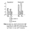
Trimethylaluminum (TMA) grade according to the present invention is stored into a canister. The canister is maintained at room temperature (20°C). Oxygen plasma is used as oxygen source (TMA will not react with oxygen gas under the conditions below). Oxygen gas is continuously introduced at a flow of 50sccm. The silicon substrate is heated at 200°C. TMA is vapour drawn but nitrogen can optionally be used as a carrier gas at a flow of about for example 50 sccm. The aluminum precursor is sequentially introduced into the reaction chamber. During the first step, a pulse of trimethylaluminum is introduced during 20ms, followed by an optional 3.5 s argon purge. A pulse of plasma is generated into the reaction chamber during 3 s to produce oxygen plasma, followed by the optional 0.5 s argon purge. This first sequence is then repeated 1000 times. An Al2O3 film meeting the electrical properties requirements (charge carrier lifetime of silicon substrate) for photovoltaic applications is obtained. Such a good result shows that the usage of a "non-semiconductor grade" is possible for deposition of an Al2O3 layer having proficient passivation properties. - 3) Deposition tests were performed with a "semiconductor grade" (the highest grade available, see Table 1 for some typical impurity levels) and a "non-semiconductor grade" (see Table 2) TMA samples. Resulting recombination velocities of minority carriers (before and after a 400°C annealing step) are given (see
Figure 4 ) for 20 nm thick Al2O3 layer deposited by thermal ALD and plasma ALD using a "semiconductor grade" (highest purity) and a "non-semiconductor grade" according to the present invention.Figure 4 shows that the results of the Al2O3 layer deposited from TMA by "non-semiconductor grade" according to the present invention are equivalent to the results of the Al2O3 layer deposited from TMA by "semiconductor grade". - Taking into consideration the background of the invention, the conclusion of these tests is very surprising and it opens up a new possibility for manufacturing of crystalline silicon wafer based photovoltaic solar cells thanks to this innovative "non-semiconductor grade" trialkylaluminum solution for deposition of surface passivation alumina layer. Also for any photovoltaic devices, encapsulation issues can be addressed by Atomic Layer Deposition of Al2O3 deposited with "non-semiconductor grade" trialkylaluminum.
- It was demonstrated that the deposition of Al2O3 for passivation can be performed from a "non-semiconductor grade" of trialkylaluminum such as TMA and TEA as aluminum source without observable degradation of the crystalline silicon wafer based photovoltaic solar cells' performance; and more precisely without harming the passivation capability of the surface alumina layer.
| Non- Semiconductor grade of the invention (ppbw) | ||
| B | Boron | 5,000 |
| Ca | Calcium | 5,000 |
| Cr | Chromium | 5,000 |
| Cu | Copper | 5,000 |
| Fe | Iron | 3,000 |
| K | Potassium | 10,000 |
| Na | Sodium | 6,000 |
| Ni | Nickel | 10,000 |
| Zn | Zinc | 10,000 |
| Ti | Titanium | 5,000 |
| Sn | Tin | 5,000 |
| Mo | Molybdenum | 2,000 |
| Ta | Tantalum | 2,000 |
| W | Tungsten | 10,000 |
| Min (ppbw) | Recommended values (ppbw) | Max (ppbw) | ||
| B | Boron | 0 | 5000 | 20000 |
| Ca | Calcium | 0 | 5000 | 20000 |
| Cr | Chromium | 0 | 5000 | 20000 |
| Cu | Copper | 2000 | 5000 | 5000 |
| Fe | Iron | 1000 | 3000 | 5000 |
| K | Potassium | 0 | 10000 | 20000 |
| Na | Sodium | 0 | 6000 | 20000 |
| Ni | Nickel | 5000 | 10000 | 10000 |
| Zn | Zinc | 2000 | 10000 | 10000 |
| Ti | Titanium | 0 | 5000 | 20000 |
| Sn | Tin | 0 | 5000 | 20000 |
| Mo | Molybdenum | 200 | 2000 | 5000 |
| Ta | Tantalum | 200 | 2000 | 5000 |
| W | Tungsten | 500 | 10000 | 10000 |
| Nb | Niobium | 0 | 10000 | 20000 |
| Mn | Manganese | 0 | 5000 | 20000 |
| Co | Cobalt | 0 | 5000 | 20000 |
Claims (12)
- A composition comprising, for 100% of its total mass, at least 97% of a Trialkylaluminium and :- From 200 ppb to 5 ppm of Mo (Molybdenum);- From 1000 ppb to 5 ppm of Fe (Iron);- From 200 ppb to 5 ppm of Cu (Copper);- From 200 ppb to 10 ppm of Ta (Tantalum).
- Composition of claim 1 comprising also:- From 5000 ppb to 10 ppm of Ni (Nickel);- From 2000 ppb to 10 ppm of Zn (Zinc);- From 5000 ppb to 10 ppm of W (Tungsten).
- Composition of claim 1 or 2 comprising other metal impurities such as B (Boron), Ca (Calcium), K (Potassium), Cr (Chromium), Na (Sodium), Nb (Niobium), Ti (Titanium), Mn (Manganese), Co (Cobalt), Sn (Tin) in a quantity comprised between 0 and 20ppm for each of them.
- Composition of any of claims 1 to 3, wherein the Trialkylaluminium is selected from Trimethylaluminum and Triethylaluminum.
- Use of a composition as defined in anyone of claims 1 to 4 for a thin film deposition method by ALD, PEALD, CVD, PECVD or MOCVD.
- Use according to claim 5, wherein the deposition method is an ALD method.
- Use of claim 5 or 6 wherein the thin film is a film of Al2O3.
- Use according to anyone of claims 5 to 7 for Al2O3 growth for photovoltaic applications.
- Use according to anyone of claims 5 to 8 wherein the composition of claims 1 to 3 comprises from 97% to 99,4% of Trialkylaluminium selected from Trimethylaluminum and Triethylaluminum.
- Film of Al2O3 obtained by the use as defined in anyone of claims 5 to 9.
- Use of the film defined in Claim 10 for the passivation of photovoltaic devices, in particular for solar cells.
- Use of the film defined in Claim 10 for the encapsulation of photovoltaic devices, in particular for solar cells.
Priority Applications (5)
| Application Number | Priority Date | Filing Date | Title |
|---|---|---|---|
| EP10305955.6A EP2426136B1 (en) | 2010-09-03 | 2010-09-03 | Use of trialkylaluminum for the growth of Al2O3 thin films for photovoltaic applications |
| CN201180042555.7A CN103080115B (en) | 2010-09-03 | 2011-08-25 | Growth of Al2O3 thin films from trialkylaluminum for photovoltaic applications |
| MYPI2013000538A MY157831A (en) | 2010-09-03 | 2011-08-25 | Growth of al2o3 thin films from trialkyllaluminum for photovoltaic applications |
| BR112013005133A BR112013005133A2 (en) | 2010-09-03 | 2011-08-25 | trialkylaluminum al203 thin film growth for photovoltaic applications |
| PCT/EP2011/064675 WO2012028539A1 (en) | 2010-09-03 | 2011-08-25 | Growth of al2o3 thin films from trialkyllaluminum for photovoltaic applications |
Applications Claiming Priority (1)
| Application Number | Priority Date | Filing Date | Title |
|---|---|---|---|
| EP10305955.6A EP2426136B1 (en) | 2010-09-03 | 2010-09-03 | Use of trialkylaluminum for the growth of Al2O3 thin films for photovoltaic applications |
Publications (2)
| Publication Number | Publication Date |
|---|---|
| EP2426136A1 true EP2426136A1 (en) | 2012-03-07 |
| EP2426136B1 EP2426136B1 (en) | 2013-05-01 |
Family
ID=43480993
Family Applications (1)
| Application Number | Title | Priority Date | Filing Date |
|---|---|---|---|
| EP10305955.6A Active EP2426136B1 (en) | 2010-09-03 | 2010-09-03 | Use of trialkylaluminum for the growth of Al2O3 thin films for photovoltaic applications |
Country Status (5)
| Country | Link |
|---|---|
| EP (1) | EP2426136B1 (en) |
| CN (1) | CN103080115B (en) |
| BR (1) | BR112013005133A2 (en) |
| MY (1) | MY157831A (en) |
| WO (1) | WO2012028539A1 (en) |
Cited By (1)
| Publication number | Priority date | Publication date | Assignee | Title |
|---|---|---|---|---|
| EP3327173A1 (en) * | 2016-11-29 | 2018-05-30 | Total SA | Method for depositing a layer of chalcogenide on a substrate |
Families Citing this family (1)
| Publication number | Priority date | Publication date | Assignee | Title |
|---|---|---|---|---|
| CN116426010A (en) * | 2021-12-31 | 2023-07-14 | 广东聚华印刷显示技术有限公司 | Composite thin film, preparation method thereof, and display device |
Citations (2)
| Publication number | Priority date | Publication date | Assignee | Title |
|---|---|---|---|---|
| US20100090218A1 (en) * | 2008-10-10 | 2010-04-15 | Jiro Tsukahara | Sealed device |
| DE102009003467A1 (en) * | 2009-02-11 | 2010-08-19 | Q-Cells Se | Rear-contacted solar cell |
-
2010
- 2010-09-03 EP EP10305955.6A patent/EP2426136B1/en active Active
-
2011
- 2011-08-25 MY MYPI2013000538A patent/MY157831A/en unknown
- 2011-08-25 BR BR112013005133A patent/BR112013005133A2/en not_active Application Discontinuation
- 2011-08-25 CN CN201180042555.7A patent/CN103080115B/en not_active Expired - Fee Related
- 2011-08-25 WO PCT/EP2011/064675 patent/WO2012028539A1/en not_active Ceased
Patent Citations (2)
| Publication number | Priority date | Publication date | Assignee | Title |
|---|---|---|---|---|
| US20100090218A1 (en) * | 2008-10-10 | 2010-04-15 | Jiro Tsukahara | Sealed device |
| DE102009003467A1 (en) * | 2009-02-11 | 2010-08-19 | Q-Cells Se | Rear-contacted solar cell |
Non-Patent Citations (10)
| Title |
|---|
| A.A. ISTRATOV; C. FLINK; H. HIESLMAIR; S.A. MCHUGO; E.R. WEBER: "Diffusion, solubility and gettring of copper in silicon", MATERIALS SCIENCE AND ENGINEERING, vol. B72, 2000, pages 99 - 104 |
| AGOSTINELLI ET AL.: "Very Low surface recombination velocities on p-type silicon wafers passivated with a dielectric with fixed negative charge", SOLAR ENERGY MATERIALS & SOLAR CELLS, vol. 90, 2006, pages 3438 - 3443 |
| CAS ET AL.: "Very low surface recombination velocity on p-type c-Si by high-rate plasma-deposited aluminum oxide", APPLIED PHYSICS LETTERS, vol. 95, 2009 |
| DINGEMANS G ET AL: "Silicon surface passivation by ultrathin Al2O3 films synthesized by thermal and plasma atomic layer deposition", PHYSICA STATUS SOLIDI - RAPID RESEARCH LETTERS 2010 WILEY-VCH VERLAG DEU, vol. 4, no. 1-2, February 2010 (2010-02-01), pages 10 - 12, XP002619642, DOI: 10.1002/PSSR.200903334 * |
| HEMMEN VAN J L ET AL: "PLASMA AND THERMAL ALD OF AL2O3 IN A COMMERCIAL 200 MM ALD REACTOR", JOURNAL OF THE ELECTROCHEMICAL SOCIETY, PHILADELPHIA, US, US, vol. 154, no. 7, 1 July 2007 (2007-07-01), pages G165 - G169, XP001544016 * |
| HOEX ET AL.: "Silicon surface passivation by atomic layer deposited A1203", JOURNAL OF APPLIED PHYSICS, vol. 104, 2008, pages 044903 |
| P.VITANOV: "Chemical Deposition of AI203 thin films on Si substrates", THIN SOLID FILMS, vol. 517, 2009, pages 6327 - 6330 |
| POODT P ET AL: "High-speed spatial atomic-layer deposition of aluminum oxide layers for solar cell passivation", ADVANCED MATERIALS 20100824 WILEY-VCH VERLAG DEU, vol. 22, no. 32, 24 August 2010 (2010-08-24), pages 3564 - 3567, XP002619643, DOI: 10.1002/ADMA.201000766 * |
| V.G. LITOVCHENKO; N.I. KLYUIS; A.A. EVTUKH; A.A. EFREMOV; A.V. SARIKOV ET AL.: "Solar cells prepared on multicrystalline silicon subjected to new gettering and passivation treatments", SOLAR ENERGY MATERIALS AND SOLAR CELLS, vol. 72, 2002, pages 343 - 351 |
| ZOTH ET AL.: "Analytical and Diagnostic Techniques for Semiconductor Materials, Devices and Processes", 1999, THE ELECTROCHEMICAL SOCIETY PROCEEDINGS, article "Silicon contamination control by lifetime measurements" |
Cited By (2)
| Publication number | Priority date | Publication date | Assignee | Title |
|---|---|---|---|---|
| EP3327173A1 (en) * | 2016-11-29 | 2018-05-30 | Total SA | Method for depositing a layer of chalcogenide on a substrate |
| FR3059340A1 (en) * | 2016-11-29 | 2018-06-01 | Total Sa | METHOD FOR DEPOSITION OF CHALCOGENURE LAYER ON A SUBSTRATE |
Also Published As
| Publication number | Publication date |
|---|---|
| BR112013005133A2 (en) | 2018-04-24 |
| WO2012028539A1 (en) | 2012-03-08 |
| CN103080115A (en) | 2013-05-01 |
| EP2426136B1 (en) | 2013-05-01 |
| MY157831A (en) | 2016-07-29 |
| CN103080115B (en) | 2015-05-06 |
Similar Documents
| Publication | Publication Date | Title |
|---|---|---|
| EP2426233B1 (en) | Use of dialkyl monoalkoxy aluminum for the growth of Al2O3 thin films for photovoltaic applications | |
| CN103476965B (en) | By the method for aluminium and silicon precursor depositing Al 2O3/SiO2 lamination | |
| KR101664504B1 (en) | Solar cell, and method of manufacturing the same | |
| Johnson et al. | A brief review of atomic layer deposition: from fundamentals to applications | |
| CN101573782B (en) | Semiconductor layer manufacturing method, semiconductor layer manufacturing apparatus and semiconductor device manufactured by using such method and apparatus | |
| KR20220084440A (en) | Photoactive devices and materials | |
| EP2484801B1 (en) | Method of deposition of Al2O3/SiO2 stacks, from TMA or TEA and silicon precursors | |
| JP4020748B2 (en) | Manufacturing method of solar cell | |
| KR20190040354A (en) | Metal complexes containing allyl ligands | |
| WO2014083241A1 (en) | Method for fabricating a passivation film on a crystalline silicon surface | |
| EP2426136B1 (en) | Use of trialkylaluminum for the growth of Al2O3 thin films for photovoltaic applications | |
| WO2009075585A1 (en) | Method of depositing a doped zinc oxide film, a conductive zinc oxide film and use of the doped zinc oxide film | |
| EP2484803B1 (en) | Method of deposition of Al2O3/SiO2 stacks, from aluminium and silicon precursors | |
| EP2484802B1 (en) | Method of deposition of Al2O3/SiO2 stacks from DMAI and silicon precursors | |
| Waki et al. | Mechanism for low temperature activation of Mg-doped GaN with Ni catalysts | |
| JP6951734B2 (en) | Copper nitride semiconductor and its manufacturing method | |
| WO2014080080A1 (en) | Method for fabricating a passivation film on a crystalline silicon surface | |
| CN120129333A (en) | Method for preparing silicon wafer boron-doped layer, silicon wafer and device system | |
| Hong et al. | Structural and electrical characterization of microcrystalline silicon films prepared by a layer-by-layer technique with a plasma-enhanced chemical-vapor deposition system | |
| CN121815931A (en) | Electron transport layer, solar cell and preparation method | |
| Cohan | Chemical Vapor Deposition and Physical Vapor Deposition of Wide Bandgap Metal Sulfides for Photovoltaic Devices | |
| Utsumi | Low‐temperature B doping of Si by synchrotron radiation irradiation of disilane/decaborane during gas‐source molecular beam epitaxy | |
| CN120475852A (en) | A passivation method for silicon solar cells, a preparation method for silicon-calcium stacked cells and a device | |
| TW202509262A (en) | Method for producing tin(II) oxide thin film | |
| Yasutake et al. | Chemical Transport Deposition of Purified Poly-Si Films from Metallurgical-grade Si Using Subatmospheric-pressure H2 Plasma |
Legal Events
| Date | Code | Title | Description |
|---|---|---|---|
| AK | Designated contracting states |
Kind code of ref document: A1 Designated state(s): AL AT BE BG CH CY CZ DE DK EE ES FI FR GB GR HR HU IE IS IT LI LT LU LV MC MK MT NL NO PL PT RO SE SI SK SM TR |
|
| AX | Request for extension of the european patent |
Extension state: BA ME RS |
|
| PUAI | Public reference made under article 153(3) epc to a published international application that has entered the european phase |
Free format text: ORIGINAL CODE: 0009012 |
|
| 17P | Request for examination filed |
Effective date: 20120907 |
|
| GRAP | Despatch of communication of intention to grant a patent |
Free format text: ORIGINAL CODE: EPIDOSNIGR1 |
|
| RIC1 | Information provided on ipc code assigned before grant |
Ipc: C07F 5/06 20060101AFI20121022BHEP Ipc: H01L 31/0216 20060101ALN20121022BHEP Ipc: C23C 16/455 20060101ALI20121022BHEP |
|
| RIC1 | Information provided on ipc code assigned before grant |
Ipc: C07F 5/06 20060101AFI20121031BHEP Ipc: C23C 16/455 20060101ALI20121031BHEP Ipc: H01L 31/0216 20060101ALN20121031BHEP |
|
| GRAS | Grant fee paid |
Free format text: ORIGINAL CODE: EPIDOSNIGR3 |
|
| GRAA | (expected) grant |
Free format text: ORIGINAL CODE: 0009210 |
|
| AK | Designated contracting states |
Kind code of ref document: B1 Designated state(s): AL AT BE BG CH CY CZ DE DK EE ES FI FR GB GR HR HU IE IS IT LI LT LU LV MC MK MT NL NO PL PT RO SE SI SK SM TR |
|
| REG | Reference to a national code |
Ref country code: GB Ref legal event code: FG4D |
|
| REG | Reference to a national code |
Ref country code: CH Ref legal event code: EP Ref country code: AT Ref legal event code: REF Ref document number: 609897 Country of ref document: AT Kind code of ref document: T Effective date: 20130515 |
|
| REG | Reference to a national code |
Ref country code: IE Ref legal event code: FG4D |
|
| REG | Reference to a national code |
Ref country code: DE Ref legal event code: R096 Ref document number: 602010006653 Country of ref document: DE Effective date: 20130627 |
|
| REG | Reference to a national code |
Ref country code: AT Ref legal event code: MK05 Ref document number: 609897 Country of ref document: AT Kind code of ref document: T Effective date: 20130501 |
|
| REG | Reference to a national code |
Ref country code: NL Ref legal event code: VDEP Effective date: 20130501 |
|
| REG | Reference to a national code |
Ref country code: LT Ref legal event code: MG4D |
|
| PG25 | Lapsed in a contracting state [announced via postgrant information from national office to epo] |
Ref country code: ES Free format text: LAPSE BECAUSE OF FAILURE TO SUBMIT A TRANSLATION OF THE DESCRIPTION OR TO PAY THE FEE WITHIN THE PRESCRIBED TIME-LIMIT Effective date: 20130812 Ref country code: SE Free format text: LAPSE BECAUSE OF FAILURE TO SUBMIT A TRANSLATION OF THE DESCRIPTION OR TO PAY THE FEE WITHIN THE PRESCRIBED TIME-LIMIT Effective date: 20130501 Ref country code: GR Free format text: LAPSE BECAUSE OF FAILURE TO SUBMIT A TRANSLATION OF THE DESCRIPTION OR TO PAY THE FEE WITHIN THE PRESCRIBED TIME-LIMIT Effective date: 20130802 Ref country code: LT Free format text: LAPSE BECAUSE OF FAILURE TO SUBMIT A TRANSLATION OF THE DESCRIPTION OR TO PAY THE FEE WITHIN THE PRESCRIBED TIME-LIMIT Effective date: 20130501 Ref country code: NO Free format text: LAPSE BECAUSE OF FAILURE TO SUBMIT A TRANSLATION OF THE DESCRIPTION OR TO PAY THE FEE WITHIN THE PRESCRIBED TIME-LIMIT Effective date: 20130801 Ref country code: IS Free format text: LAPSE BECAUSE OF FAILURE TO SUBMIT A TRANSLATION OF THE DESCRIPTION OR TO PAY THE FEE WITHIN THE PRESCRIBED TIME-LIMIT Effective date: 20130901 Ref country code: AT Free format text: LAPSE BECAUSE OF FAILURE TO SUBMIT A TRANSLATION OF THE DESCRIPTION OR TO PAY THE FEE WITHIN THE PRESCRIBED TIME-LIMIT Effective date: 20130501 Ref country code: SI Free format text: LAPSE BECAUSE OF FAILURE TO SUBMIT A TRANSLATION OF THE DESCRIPTION OR TO PAY THE FEE WITHIN THE PRESCRIBED TIME-LIMIT Effective date: 20130501 Ref country code: FI Free format text: LAPSE BECAUSE OF FAILURE TO SUBMIT A TRANSLATION OF THE DESCRIPTION OR TO PAY THE FEE WITHIN THE PRESCRIBED TIME-LIMIT Effective date: 20130501 Ref country code: PT Free format text: LAPSE BECAUSE OF FAILURE TO SUBMIT A TRANSLATION OF THE DESCRIPTION OR TO PAY THE FEE WITHIN THE PRESCRIBED TIME-LIMIT Effective date: 20130902 |
|
| PG25 | Lapsed in a contracting state [announced via postgrant information from national office to epo] |
Ref country code: CY Free format text: LAPSE BECAUSE OF FAILURE TO SUBMIT A TRANSLATION OF THE DESCRIPTION OR TO PAY THE FEE WITHIN THE PRESCRIBED TIME-LIMIT Effective date: 20130501 Ref country code: PL Free format text: LAPSE BECAUSE OF FAILURE TO SUBMIT A TRANSLATION OF THE DESCRIPTION OR TO PAY THE FEE WITHIN THE PRESCRIBED TIME-LIMIT Effective date: 20130501 Ref country code: HR Free format text: LAPSE BECAUSE OF FAILURE TO SUBMIT A TRANSLATION OF THE DESCRIPTION OR TO PAY THE FEE WITHIN THE PRESCRIBED TIME-LIMIT Effective date: 20130501 Ref country code: BG Free format text: LAPSE BECAUSE OF FAILURE TO SUBMIT A TRANSLATION OF THE DESCRIPTION OR TO PAY THE FEE WITHIN THE PRESCRIBED TIME-LIMIT Effective date: 20130801 |
|
| PG25 | Lapsed in a contracting state [announced via postgrant information from national office to epo] |
Ref country code: LV Free format text: LAPSE BECAUSE OF FAILURE TO SUBMIT A TRANSLATION OF THE DESCRIPTION OR TO PAY THE FEE WITHIN THE PRESCRIBED TIME-LIMIT Effective date: 20130501 |
|
| PG25 | Lapsed in a contracting state [announced via postgrant information from national office to epo] |
Ref country code: CZ Free format text: LAPSE BECAUSE OF FAILURE TO SUBMIT A TRANSLATION OF THE DESCRIPTION OR TO PAY THE FEE WITHIN THE PRESCRIBED TIME-LIMIT Effective date: 20130501 Ref country code: DK Free format text: LAPSE BECAUSE OF FAILURE TO SUBMIT A TRANSLATION OF THE DESCRIPTION OR TO PAY THE FEE WITHIN THE PRESCRIBED TIME-LIMIT Effective date: 20130501 Ref country code: EE Free format text: LAPSE BECAUSE OF FAILURE TO SUBMIT A TRANSLATION OF THE DESCRIPTION OR TO PAY THE FEE WITHIN THE PRESCRIBED TIME-LIMIT Effective date: 20130501 Ref country code: SK Free format text: LAPSE BECAUSE OF FAILURE TO SUBMIT A TRANSLATION OF THE DESCRIPTION OR TO PAY THE FEE WITHIN THE PRESCRIBED TIME-LIMIT Effective date: 20130501 |
|
| PG25 | Lapsed in a contracting state [announced via postgrant information from national office to epo] |
Ref country code: RO Free format text: LAPSE BECAUSE OF FAILURE TO SUBMIT A TRANSLATION OF THE DESCRIPTION OR TO PAY THE FEE WITHIN THE PRESCRIBED TIME-LIMIT Effective date: 20130501 Ref country code: IT Free format text: LAPSE BECAUSE OF FAILURE TO SUBMIT A TRANSLATION OF THE DESCRIPTION OR TO PAY THE FEE WITHIN THE PRESCRIBED TIME-LIMIT Effective date: 20130501 Ref country code: NL Free format text: LAPSE BECAUSE OF FAILURE TO SUBMIT A TRANSLATION OF THE DESCRIPTION OR TO PAY THE FEE WITHIN THE PRESCRIBED TIME-LIMIT Effective date: 20130501 |
|
| PLBE | No opposition filed within time limit |
Free format text: ORIGINAL CODE: 0009261 |
|
| STAA | Information on the status of an ep patent application or granted ep patent |
Free format text: STATUS: NO OPPOSITION FILED WITHIN TIME LIMIT |
|
| 26N | No opposition filed |
Effective date: 20140204 |
|
| PG25 | Lapsed in a contracting state [announced via postgrant information from national office to epo] |
Ref country code: MC Free format text: LAPSE BECAUSE OF FAILURE TO SUBMIT A TRANSLATION OF THE DESCRIPTION OR TO PAY THE FEE WITHIN THE PRESCRIBED TIME-LIMIT Effective date: 20130501 |
|
| REG | Reference to a national code |
Ref country code: DE Ref legal event code: R097 Ref document number: 602010006653 Country of ref document: DE Effective date: 20140204 |
|
| REG | Reference to a national code |
Ref country code: IE Ref legal event code: MM4A |
|
| PG25 | Lapsed in a contracting state [announced via postgrant information from national office to epo] |
Ref country code: IE Free format text: LAPSE BECAUSE OF NON-PAYMENT OF DUE FEES Effective date: 20130903 |
|
| REG | Reference to a national code |
Ref country code: CH Ref legal event code: PL |
|
| GBPC | Gb: european patent ceased through non-payment of renewal fee |
Effective date: 20140903 |
|
| PG25 | Lapsed in a contracting state [announced via postgrant information from national office to epo] |
Ref country code: SM Free format text: LAPSE BECAUSE OF FAILURE TO SUBMIT A TRANSLATION OF THE DESCRIPTION OR TO PAY THE FEE WITHIN THE PRESCRIBED TIME-LIMIT Effective date: 20130501 |
|
| PG25 | Lapsed in a contracting state [announced via postgrant information from national office to epo] |
Ref country code: MT Free format text: LAPSE BECAUSE OF FAILURE TO SUBMIT A TRANSLATION OF THE DESCRIPTION OR TO PAY THE FEE WITHIN THE PRESCRIBED TIME-LIMIT Effective date: 20130501 Ref country code: TR Free format text: LAPSE BECAUSE OF FAILURE TO SUBMIT A TRANSLATION OF THE DESCRIPTION OR TO PAY THE FEE WITHIN THE PRESCRIBED TIME-LIMIT Effective date: 20130501 |
|
| PG25 | Lapsed in a contracting state [announced via postgrant information from national office to epo] |
Ref country code: CH Free format text: LAPSE BECAUSE OF NON-PAYMENT OF DUE FEES Effective date: 20140930 Ref country code: GB Free format text: LAPSE BECAUSE OF NON-PAYMENT OF DUE FEES Effective date: 20140903 Ref country code: HU Free format text: LAPSE BECAUSE OF FAILURE TO SUBMIT A TRANSLATION OF THE DESCRIPTION OR TO PAY THE FEE WITHIN THE PRESCRIBED TIME-LIMIT; INVALID AB INITIO Effective date: 20100903 Ref country code: LI Free format text: LAPSE BECAUSE OF NON-PAYMENT OF DUE FEES Effective date: 20140930 Ref country code: MK Free format text: LAPSE BECAUSE OF FAILURE TO SUBMIT A TRANSLATION OF THE DESCRIPTION OR TO PAY THE FEE WITHIN THE PRESCRIBED TIME-LIMIT Effective date: 20130501 Ref country code: LU Free format text: LAPSE BECAUSE OF NON-PAYMENT OF DUE FEES Effective date: 20130903 |
|
| REG | Reference to a national code |
Ref country code: FR Ref legal event code: PLFP Year of fee payment: 7 |
|
| REG | Reference to a national code |
Ref country code: FR Ref legal event code: PLFP Year of fee payment: 8 |
|
| REG | Reference to a national code |
Ref country code: FR Ref legal event code: PLFP Year of fee payment: 9 |
|
| PG25 | Lapsed in a contracting state [announced via postgrant information from national office to epo] |
Ref country code: AL Free format text: LAPSE BECAUSE OF FAILURE TO SUBMIT A TRANSLATION OF THE DESCRIPTION OR TO PAY THE FEE WITHIN THE PRESCRIBED TIME-LIMIT Effective date: 20130501 |
|
| PGFP | Annual fee paid to national office [announced via postgrant information from national office to epo] |
Ref country code: DE Payment date: 20220920 Year of fee payment: 13 |
|
| PGFP | Annual fee paid to national office [announced via postgrant information from national office to epo] |
Ref country code: BE Payment date: 20220920 Year of fee payment: 13 |
|
| REG | Reference to a national code |
Ref country code: DE Ref legal event code: R119 Ref document number: 602010006653 Country of ref document: DE |
|
| REG | Reference to a national code |
Ref country code: BE Ref legal event code: MM Effective date: 20230930 |
|
| PG25 | Lapsed in a contracting state [announced via postgrant information from national office to epo] |
Ref country code: DE Free format text: LAPSE BECAUSE OF NON-PAYMENT OF DUE FEES Effective date: 20240403 |
|
| PG25 | Lapsed in a contracting state [announced via postgrant information from national office to epo] |
Ref country code: BE Free format text: LAPSE BECAUSE OF NON-PAYMENT OF DUE FEES Effective date: 20230930 |
|
| PGFP | Annual fee paid to national office [announced via postgrant information from national office to epo] |
Ref country code: FR Payment date: 20250922 Year of fee payment: 16 |