EP2425528B1 - Power amplifier - Google Patents
Power amplifier Download PDFInfo
- Publication number
- EP2425528B1 EP2425528B1 EP10726642.1A EP10726642A EP2425528B1 EP 2425528 B1 EP2425528 B1 EP 2425528B1 EP 10726642 A EP10726642 A EP 10726642A EP 2425528 B1 EP2425528 B1 EP 2425528B1
- Authority
- EP
- European Patent Office
- Prior art keywords
- input
- signal
- circuit
- integrator
- gain
- Prior art date
- Legal status (The legal status is an assumption and is not a legal conclusion. Google has not performed a legal analysis and makes no representation as to the accuracy of the status listed.)
- Not-in-force
Links
- 238000001914 filtration Methods 0.000 claims description 4
- 238000000034 method Methods 0.000 claims description 3
- 230000003321 amplification Effects 0.000 claims 1
- 238000003199 nucleic acid amplification method Methods 0.000 claims 1
- 238000010586 diagram Methods 0.000 description 10
- 239000003990 capacitor Substances 0.000 description 6
- 230000007423 decrease Effects 0.000 description 5
- 230000010355 oscillation Effects 0.000 description 4
- 230000008901 benefit Effects 0.000 description 3
- 230000003247 decreasing effect Effects 0.000 description 2
- 238000011045 prefiltration Methods 0.000 description 2
- 230000004044 response Effects 0.000 description 2
- 238000012935 Averaging Methods 0.000 description 1
- 230000001066 destructive effect Effects 0.000 description 1
- 230000006872 improvement Effects 0.000 description 1
- 238000012986 modification Methods 0.000 description 1
- 230000004048 modification Effects 0.000 description 1
- 230000010363 phase shift Effects 0.000 description 1
- 239000002994 raw material Substances 0.000 description 1
- 238000000926 separation method Methods 0.000 description 1
- 238000004088 simulation Methods 0.000 description 1
Images


Classifications
-
- H—ELECTRICITY
- H03—ELECTRONIC CIRCUITRY
- H03F—AMPLIFIERS
- H03F3/00—Amplifiers with only discharge tubes or only semiconductor devices as amplifying elements
- H03F3/20—Power amplifiers, e.g. Class B amplifiers, Class C amplifiers
- H03F3/21—Power amplifiers, e.g. Class B amplifiers, Class C amplifiers with semiconductor devices only
- H03F3/217—Class D power amplifiers; Switching amplifiers
-
- H—ELECTRICITY
- H03—ELECTRONIC CIRCUITRY
- H03F—AMPLIFIERS
- H03F3/00—Amplifiers with only discharge tubes or only semiconductor devices as amplifying elements
- H03F3/20—Power amplifiers, e.g. Class B amplifiers, Class C amplifiers
- H03F3/21—Power amplifiers, e.g. Class B amplifiers, Class C amplifiers with semiconductor devices only
- H03F3/217—Class D power amplifiers; Switching amplifiers
- H03F3/2173—Class D power amplifiers; Switching amplifiers of the bridge type
-
- H—ELECTRICITY
- H03—ELECTRONIC CIRCUITRY
- H03G—CONTROL OF AMPLIFICATION
- H03G3/00—Gain control in amplifiers or frequency changers
- H03G3/20—Automatic control
- H03G3/30—Automatic control in amplifiers having semiconductor devices
- H03G3/3005—Automatic control in amplifiers having semiconductor devices in amplifiers suitable for low-frequencies, e.g. audio amplifiers
Definitions
- Power amplifier for amplifying an electric input signal in an operational frequency range and providing an output signal, comprising switching means for generating a block wave signal by alternately switching the block wave signal to a first supply voltage or a second supply voltage, filter means for generating a power output signal by low pass filtering the block wave signal, input means for receiving the electric signal and driving the switching means, and a local feedback circuit connecting the output signal to an input of the switching means.
- Switching power amplifiers also referred to as pulse modulation amplifiers, pulse width modulation (PWM) amplifiers or class D amplifiers are commonly used in applications where power dissipation is an important factor.
- PWM pulse width modulation
- Class d amplifiers are important for lowering power consumption and decreasing the size/weight and hence the use of raw materials.
- Such amplifiers there is an input stage for receiving an electrical input signal to be amplified, a modulating/switching or power stage and a filter.
- the switching stage generates a block wave signal, or a pulse train, which has a frequency that is much higher than the highest frequency in the operational frequency range of the electric signal to be amplified.
- the pulse width ratio of the block wave is modulated so that the average value of the block wave signal is proportional to the input signal.
- the filter filters the block wave signal to a power output signal.
- class d amplifiers Another definition of class d amplifiers is that the power stage which delivers the energy to the load is operated in an "on/off" state where the average voltage value of this square wave is modulated to correspond to the set value. The only losses that appear are the low conduction losses during the "on” state and the switching losses from each time the output stage changes state.
- a class d amplifier contains a second order low pass filter with a preferably high Q value for demodulating the PWM pulses. This filter shifts the phase assymptotically towards -180° and the higher the Q value the faster it reaches -180°. When the filter is loaded the Q value decreases.
- the actual pulse width modulation can be performed in several different ways.
- the most obvious way is to use a reference signal, for example a tri wave signal and then compare the input or set value to this reference signal. Each time those signals intersect the output stage changes state.
- a disadvantage with this reference signal technique is that the average value of the pulse train only corresponds to the set value as long as the supply voltages are constant and the state shift is infinitely fast plus of course, the tri wave has to be ideal.
- the reference signal technique does not have any feedback what so ever resulting in an absence of control over the demodulation filter. There is actually two signal paths, one from the input to the output and one from the supply rails to the output. The channel separation and power supply rejection become very poor.
- One single advantage is that the switching frequency is constant. Supply feed forward can be used to lower the supply voltage dependence.
- Using a digital device as a DSP for calculating the pulse width instead of comparing the set value to a tri wave signal basically gives the same result. However there are more possibilities to compensate for non ideal features of components. A DSP solution also is more complicated and expensive.
- a very effective way of providing the pulse width modulation is by self oscillation.
- a comparator is used to compare the average of the pulse train to the set value and if the error is negative the positive switch is turned on and vice versa if it is positive.
- the frequency of operation is close to the frequency where the loop has -180° phase shift.
- a later prior art document is WO03/090343 disclosing a power amplifier for amplifying an electric signal in an operational frequency range comprising switching means for generating a block wave signal by alternately switching the block wave signal to a first supply voltage or a second supply voltage, filter means for generating a power output signal by low pass filtering the block wave signal, input means for receiving the electric signal and driving the switching means, and a control circuit coupled to the output power signal and the input means for controlling the power amplifier.
- switching means for generating a block wave signal by alternately switching the block wave signal to a first supply voltage or a second supply voltage
- filter means for generating a power output signal by low pass filtering the block wave signal
- input means for receiving the electric signal and driving the switching means
- a control circuit coupled to the output power signal and the input means for controlling the power amplifier.
- a further option is to add a second order active integrator which demodulates the pulse train and gives an enormous amount of loop gain at low frequencies.
- the switching frequency is then entirely controlled by this integrator and not at all by the Q value of the output filter.
- the operation of this pre filter self oscillating topology is therefore very robust and simple and it gives very low non linear distorsion, especially at low frequencies.
- the drawbacks and problems of prior art amplifiers are overcome by providing a self oscillating class D amplifier having a power stage with a local feedback loop giving a local gain, and by providing a global feedback loop giving a global gain, wherein the local gain substantially is equal to the global gain.
- the local gain substantially is equal to the global gain.
- a limiter circuit is provided to measure the difference between the input and the output of the integrator and if this difference exceeds a preset threshold the limiter circuit is activated to decrease the gain of the integrator substantially and eventually to set the gain of the integrator to near unity or to unity. This means that when the class d stage can not follow the input signal, as during startup or during clipping, the integrator only has unity gain.
- a non-inverting first input of an integrator circuit 10 receives an electric input signal.
- An output of the integrator circuit 10 is connected to a switching means 12.
- a power output from the switching means 10 is connected to a low pass filter comprising an inductor 14 and a capacitor 16.
- From the inductor 14 a local feedback loop 18 connects to an inverting input of the switching means 13.
- a non-inverting input of the switching means 13 is connected to an output of the integrator circuit 10.
- a global feedback loop 20 connects the inductor 14 to an inverting second input of the integrator circuit 10.
- a limiter circuit 22 instead is connected to measure the difference between the output of the integrator circuit and the electric input signal.
- a non-inverting input of the limiter circuit is connected to the output of the integrator circuit and an inverting input of the limiter circuit is connected to receive the electric input signal.
- a limiter output is connected to the inverting second input of the integrator circuit.
- the local feedback loop results in a local gain of 1/K+1 and the integrator circuit 10 aims to keep also a global gain at 1/K+1.
- the output signal from the integrator has the same amplitude as the input signal to the integrator plus an error signal.
- the limiter circuit measures the difference between the input and the output of the integrator and if this difference exceeds a preset threshold value the limiter circuit is activated to set the gain of the integrator to near unity. This means that when the class d stage can not follow the input signal, such as during startup or during clipping, the integrator only has unity gain.
- first resistor R1 and second resistor R2 determines and can be used to adjust the amount of difference that is accepted between the input and output of the integrator circuit 10.
- a first transistor Q1 starts to conduct and decrease the output when the base - emitter voltage is about 600mV.
- R1 and R2 By choosing R1 and R2 to have a resistance of 1 kohm the maximum allowed error voltage is 1,2V.
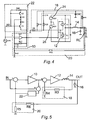
- FIG. 4 A simulation model of a post filter self oscillation class d amplifier stage with an integrator in front to increase the loop gain in the audio band is shown in Fig. 4 . Below only components with appreciable properties in a technical sense are mentioned specifically.
- a first switch S1 switches on at 0,001V and switches off at 0V.
- a second switch S2 has opposite turn on and turn of values.
- Switches S1 and S2 are connected to a first voltage source 24 and a second voltage source 26, respectively.
- Voltage sources 24 and 26 supply the required or available voltage, such as 60V in the shown embodiment.
- S1 and S2 form the switching means 12 based on a comparator and power stage.
- Resistor R44 and capacitor C19 approximate the propagation delay in the comparator - switch stage (which is there in real life).
- the local gain in the class d stage is determined by resistor R10 and resistor R8 and is fixed to be equal to the global gain, which is determined by resistor R43 and resistor R42.
- the output of the switching means 12 is fed through inductor 14 and received by a load RL.
- Amplifier circuit AR1 forms the integrator circuit 10 where capacitor C18 functions as a pole and resistor R41 limits the DC gain.
- AR1 has +/-15V as supply voltage.
- Capacitor C14 and resistor R35 pushes the switching frequency away from the filter resonance frequency up to a desired much higher frequency.
- the limiter circuit 22 is formed by resistor R45, resistor R46, transistor Q1, transistor Q2, diode D3 and diode D4. Voltage source UIN represents an electric input signal.
- a full output signal of the integrator circuit 10 is received by the limiter circuit resulting in a required gain of 1,0 of the integrator circuit 10. If a fraction of the output signal of the integrator circuit 10 is fed to the limiter circuit the required gain of the integrator circuit 10 is increased correspondingly (c.f. Fig. 8 and description) below.
- Resistors R42 and R43 form the global feedback loop 20.
- the local feedback loop 18 comprises resistors R3 and R4.
- the resulting local gain is R3/R4+1.
- the global feedback loop 20 comprises resistors R5 and R6 resulting in a global gain that is R6/R5+1.
- the alternative embodiment shown in Fig. 6 has an inverting integrator 10' and an alternative embodiment of a limiter 22' (further described with reference to Fig. 7 below).
- a local feedback loop 18' is used in a non-inverting amplifier and switching means 12 and comprises resistors R9 and R10. The resulting local gain will be R9/R10+1.
- a global feedback loop 20' comprises resistors R7 and R8 where R8 connects between the output OUT and an input of the inverting integrator 10'. The resulting global gain will be R8/R7.
- the schematic circuit diagram of Fig. 7 corresponds to the block diagram of Fig. 6 .
- Switching means 12 forms together with resistors R9 and R10 a local non-inverting amplifier.
- An inverting integrator is formed by amplifier circuit 28, resistor R11 and capacitor C11.
- Amplifier circuit 28 together with resistors R7 and R8 form an inverting integrator 10' with a global feedback loop.
- the amplifier circuit 28 has an output 29 connecting to the switching means 12.
- the alternative embodiment of the limiter 22' shown in Fig. 7 is based on a balance point between resistors R14 and R15. As long as the balance point remains at a zero value the limiter 22' is not active. However, should the output 29 of the amplifier circuit 28 start to drift off as a result of clipping the balance point will drift off from the zero value to an error value. When the error value reaches a predetermined value, in the shown embodiment about 600 mV, either transistor Q5 or transistor Q7 is activated and current is passed through either resistor R23 or resistor R24. As a result also either of transistor Q6 or transistor Q8 will conduct to decrease the error value and to prevent saturation.
- a predetermined value in the shown embodiment about 600 mV
- an integrator gain of the integrator circuit 10' is equal to R15/R14.
- the integrator gain multiplied by the gain of the local feedback loop 18' should be equal to the gain of the global feedback loop formed by resistor R7 and resistor R8.
- the switching means 12 of course can be implemented as shown in Fig. 4 and in Fig. 8 (below), respectively.
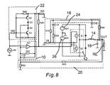
- the limiter circuit 22 is connected to compare an input signal UIN and a fraction of an output signal of the integrator circuit 10.
- the fraction is determined by resistor R25 and resistor R26. If resistor R25 is equal to resistor R26 the fraction is 1/2.
- the local feedback loop 18 has a gain of R8+R10/R8 that multiplied with an integrator gain will have to be equal, or substantially equal, to the global gain determined by resistor R42 and resistor R43.
- resistor R42 and resistor R43 By selecting resistor R42 and resistor R43 to provide a gain of 9,0 and selecting resistor R10 and resistor R8 to provide a gain of 4,5 the integrator gain will be 2,0.
- a class d amplifier stage with 1/K+1 in gain and an integrating error amplifier in front striving to produce a global gain of 1/K+1 as well and also having a limiter which compares the input signal to the output of the error amplifier and limits, by acting on the negative input of the error amplifier, the error to a desired level.
Landscapes
- Engineering & Computer Science (AREA)
- Power Engineering (AREA)
- Multimedia (AREA)
- Amplifiers (AREA)
Description
- Power amplifier for amplifying an electric input signal in an operational frequency range and providing an output signal, comprising switching means for generating a block wave signal by alternately switching the block wave signal to a first supply voltage or a second supply voltage, filter means for generating a power output signal by low pass filtering the block wave signal, input means for receiving the electric signal and driving the switching means, and a local feedback circuit connecting the output signal to an input of the switching means.
- Switching power amplifiers also referred to as pulse modulation amplifiers, pulse width modulation (PWM) amplifiers or class D amplifiers are commonly used in applications where power dissipation is an important factor. Class d amplifiers are important for lowering power consumption and decreasing the size/weight and hence the use of raw materials.
- In such amplifiers there is an input stage for receiving an electrical input signal to be amplified, a modulating/switching or power stage and a filter. The switching stage generates a block wave signal, or a pulse train, which has a frequency that is much higher than the highest frequency in the operational frequency range of the electric signal to be amplified. The pulse width ratio of the block wave is modulated so that the average value of the block wave signal is proportional to the input signal. The filter filters the block wave signal to a power output signal.
- Another definition of class d amplifiers is that the power stage which delivers the energy to the load is operated in an "on/off" state where the average voltage value of this square wave is modulated to correspond to the set value. The only losses that appear are the low conduction losses during the "on" state and the switching losses from each time the output stage changes state.
- The switching between on and off is made at a frequency which normally is around 400kHz or more giving a high enough resolution in the audible band. Normally, a class d amplifier contains a second order low pass filter with a preferably high Q value for demodulating the PWM pulses. This filter shifts the phase assymptotically towards -180° and the higher the Q value the faster it reaches -180°. When the filter is loaded the Q value decreases.
- The actual pulse width modulation can be performed in several different ways. The most obvious way is to use a reference signal, for example a tri wave signal and then compare the input or set value to this reference signal. Each time those signals intersect the output stage changes state. A disadvantage with this reference signal technique is that the average value of the pulse train only corresponds to the set value as long as the supply voltages are constant and the state shift is infinitely fast plus of course, the tri wave has to be ideal.
- The reference signal technique does not have any feedback what so ever resulting in an absence of control over the demodulation filter. There is actually two signal paths, one from the input to the output and one from the supply rails to the output. The channel separation and power supply rejection become very poor. One single advantage is that the switching frequency is constant. Supply feed forward can be used to lower the supply voltage dependence.
- Using a digital device as a DSP for calculating the pulse width instead of comparing the set value to a tri wave signal basically gives the same result. However there are more possibilities to compensate for non ideal features of components. A DSP solution also is more complicated and expensive.
- A very effective way of providing the pulse width modulation is by self oscillation. A comparator is used to compare the average of the pulse train to the set value and if the error is negative the positive switch is turned on and vice versa if it is positive. The frequency of operation is close to the frequency where the loop has -180° phase shift. Some solutions use the demodulation filter to do the averaging and this gives the amplifier the possibility to adjust errors that occur in and after the demodulation filter.
- Without additional circuitry the switching frequency would be equal to the filter resonance frequency which usually is around 50kHz and this is not acceptable. A zero and zero cancelling resistor is added in the sensing circuit to push the frequency up about a decade. This zero increases the amplitude of the modulation signal and this decreases the loop gain hence increases the non linearities. The result of this post filter self oscillating topology is therefore that the linear distorsion (distorsion which does not add new frequency content like amplitude and phase) is very low for being a class d amplifier but the non linear distorsion is poor. An early disclosure of a self oscillation class D amplifier was made by Clayton Sturgeon in Texas who filed a patent application in 1976 with serial number
US4,041,411 . - A later prior art document is
WO03/090343 US 2007/0247219 . - A further option is to add a second order active integrator which demodulates the pulse train and gives an enormous amount of loop gain at low frequencies. The switching frequency is then entirely controlled by this integrator and not at all by the Q value of the output filter. The operation of this pre filter self oscillating topology is therefore very robust and simple and it gives very low non linear distorsion, especially at low frequencies.
- However, in a pre filter self oscillating topology the linear distortion becomes high i.e. the frequency response and phase is totally load dependant and a desired response curve can only be obtained with specific load impedance. The switching frequency of all self oscillating topologies varies with the modulation depth (pulse width). This is an advantage for the efficiency as the swithing losses becomes lower as the conduction losses increase but if another loop is added to increase the loop gain there is a risk that this loop picks up the switching frequency and then the amplifier would go into a destructive sub harmonic oscillation condition.
- There is a need to increase the loop gain in order to lower the non linear and linear distorsion of self oscillating class d amplifiers. This is usually done by including an integrator which integrates the difference between the output signal and input signal, forming an error signal, to further increase the loop gain in the audible band and hence lowering the non idealities in the audible band. This gives at least one problem. At start up, before the class d stage starts to operate, or during output clipping the integrator will be fed a large error signal which will be integrated until the integrator saturates and then the error keeps charging the integrating capacitor. This causes the integrator to hang up.
- Thus, there is a desire to remove this hang up behaviour in order to be able to use an integrator in combination with a class d amplifier stage.
- In accordance with the invention the drawbacks and problems of prior art amplifiers are overcome by providing a self oscillating class D amplifier having a power stage with a local feedback loop giving a local gain, and by providing a global feedback loop giving a global gain, wherein the local gain substantially is equal to the global gain. By maintaining the local gain equal, or substantially equal, to the global gain the result will be that the output signal from the integrator has the same amplitude as the input signal to the integrator plus an error signal.
- Furthermore, a limiter circuit is provided to measure the difference between the input and the output of the integrator and if this difference exceeds a preset threshold the limiter circuit is activated to decrease the gain of the integrator substantially and eventually to set the gain of the integrator to near unity or to unity. This means that when the class d stage can not follow the input signal, as during startup or during clipping, the integrator only has unity gain.
- In order that the manner in which the above recited and other advantages and objects of the invention are obtained will be readily understood, a more particular description of the invention briefly described above will be rendered by reference to specific embodiments thereof which are illustrated in the appended drawings.
- Understanding that these drawings depict only typical embodiments of the invention and are not therefore to be considered to be limiting of its scope, the invention will be described and explained with additional specificity and detail through the use of the accompanying drawings in which:
- Fig. 1
- is a schematic block diagram of a prior art class D amplifier,
- Fig. 2
- is a schematic block diagram of a basic embodiment of an amplifier in accordance with the invention,
- Fig. 3
- is a basic circuit diagram of one embodiment of a limiter circuit included in the amplifier in accordance with the invention,
- Fig. 4
- is a schematic circuit diagram of one embodiment of an amplifier in accordance with the invention,
- Fig. 5
- is a more detailed block diagram of the embodiment of
Fig. 2 , - Fig. 6
- is a block diagram of an inverting embodiment of an amplifier in accordance with the invention,
- Fig. 7
- is a schematic circuit diagram of an inverting embodiment of an amplifier in accordance with the invention and
- Fig. 8
- is a schematic circuit diagram of an alternative embodiment of an amplifier in accordance with the invention.
- In the prior art amplifier shown in
Fig. 1 a non-inverting first input of anintegrator circuit 10 receives an electric input signal. An output of theintegrator circuit 10 is connected to a switching means 12. A power output from the switching means 10 is connected to a low pass filter comprising aninductor 14 and acapacitor 16. From the inductor 14 alocal feedback loop 18 connects to an inverting input of the switching means 13. A non-inverting input of the switching means 13 is connected to an output of theintegrator circuit 10. Aglobal feedback loop 20 connects theinductor 14 to an inverting second input of theintegrator circuit 10. During clipping conditions the integrator hangs up and this causes a high amount of audible artefacts. A possible improvement would be to keep the supply voltage at a lower level in order to limit how much the integrator hangs up but this would not solve the issues during startup or current limit situations. - In the embodiment of an amplifier in accordance with the invention shown in
Fig. 2 andFig. 5 alimiter circuit 22 instead is connected to measure the difference between the output of the integrator circuit and the electric input signal. In the embodiment shown inFig. 2 a non-inverting input of the limiter circuit is connected to the output of the integrator circuit and an inverting input of the limiter circuit is connected to receive the electric input signal. A limiter output is connected to the inverting second input of the integrator circuit. - The local feedback loop results in a local gain of 1/K+1 and the
integrator circuit 10 aims to keep also a global gain at 1/K+ 1. As a result the output signal from the integrator has the same amplitude as the input signal to the integrator plus an error signal. The limiter circuit measures the difference between the input and the output of the integrator and if this difference exceeds a preset threshold value the limiter circuit is activated to set the gain of the integrator to near unity. This means that when the class d stage can not follow the input signal, such as during startup or during clipping, the integrator only has unity gain. - In the embodiment of a limiter circuit shown in
Fig. 3 first resistor R1 and second resistor R2 determines and can be used to adjust the amount of difference that is accepted between the input and output of theintegrator circuit 10. A first transistor Q1 starts to conduct and decrease the output when the base - emitter voltage is about 600mV. By choosing R1 and R2 to have a resistance of 1 kohm the maximum allowed error voltage is 1,2V. - A simulation model of a post filter self oscillation class d amplifier stage with an integrator in front to increase the loop gain in the audio band is shown in
Fig. 4 . Below only components with appreciable properties in a technical sense are mentioned specifically. - A first switch S1 switches on at 0,001V and switches off at 0V. A second switch S2 has opposite turn on and turn of values. Switches S1 and S2 are connected to a
first voltage source 24 and asecond voltage source 26, respectively.Voltage sources inductor 14 and received by a load RL. - Amplifier circuit AR1 forms the
integrator circuit 10 where capacitor C18 functions as a pole and resistor R41 limits the DC gain. In the shown embodiment AR1 has +/-15V as supply voltage. Capacitor C14 and resistor R35 pushes the switching frequency away from the filter resonance frequency up to a desired much higher frequency. - The
limiter circuit 22 is formed by resistor R45, resistor R46, transistor Q1, transistor Q2, diode D3 and diode D4. Voltage source UIN represents an electric input signal. A full output signal of theintegrator circuit 10 is received by the limiter circuit resulting in a required gain of 1,0 of theintegrator circuit 10. If a fraction of the output signal of theintegrator circuit 10 is fed to the limiter circuit the required gain of theintegrator circuit 10 is increased correspondingly (c.f.Fig. 8 and description) below. By selecting R45 to be 1 kohm and R46 to be 10kohm the allowed error is decreased to around 600 mV. Resistors R42 and R43 form theglobal feedback loop 20. - In the embodiment shown in
Fig. 5 thelocal feedback loop 18 comprises resistors R3 and R4. The resulting local gain is R3/R4+ 1. Correspondingly theglobal feedback loop 20 comprises resistors R5 and R6 resulting in a global gain that is R6/R5+ 1. - The alternative embodiment shown in
Fig. 6 has an inverting integrator 10' and an alternative embodiment of a limiter 22' (further described with reference toFig. 7 below). A local feedback loop 18' is used in a non-inverting amplifier and switching means 12 and comprises resistors R9 and R10. The resulting local gain will be R9/R10+1. A global feedback loop 20' comprises resistors R7 and R8 where R8 connects between the output OUT and an input of the inverting integrator 10'. The resulting global gain will be R8/R7. - The schematic circuit diagram of
Fig. 7 corresponds to the block diagram ofFig. 6 . Switching means 12 forms together with resistors R9 and R10 a local non-inverting amplifier. An inverting integrator is formed byamplifier circuit 28, resistor R11 and capacitor C11.Amplifier circuit 28 together with resistors R7 and R8 form an inverting integrator 10' with a global feedback loop. Theamplifier circuit 28 has an output 29 connecting to the switching means 12. - The alternative embodiment of the limiter 22' shown in
Fig. 7 is based on a balance point between resistors R14 and R15. As long as the balance point remains at a zero value the limiter 22' is not active. However, should the output 29 of theamplifier circuit 28 start to drift off as a result of clipping the balance point will drift off from the zero value to an error value. When the error value reaches a predetermined value, in the shown embodiment about 600 mV, either transistor Q5 or transistor Q7 is activated and current is passed through either resistor R23 or resistor R24. As a result also either of transistor Q6 or transistor Q8 will conduct to decrease the error value and to prevent saturation. - In the embodiment shown in
Fig. 7 an integrator gain of the integrator circuit 10' is equal to R15/R14. The integrator gain multiplied by the gain of the local feedback loop 18' should be equal to the gain of the global feedback loop formed by resistor R7 and resistor R8. The switching means 12 of course can be implemented as shown inFig. 4 and inFig. 8 (below), respectively. - In the embodiment shown in
Fig. 8 thelimiter circuit 22 is connected to compare an input signal UIN and a fraction of an output signal of theintegrator circuit 10. The fraction is determined by resistor R25 and resistor R26. If resistor R25 is equal to resistor R26 the fraction is 1/2. In this case thelocal feedback loop 18 has a gain of R8+R10/R8 that multiplied with an integrator gain will have to be equal, or substantially equal, to the global gain determined by resistor R42 and resistor R43. By selecting resistor R42 and resistor R43 to provide a gain of 9,0 and selecting resistor R10 and resistor R8 to provide a gain of 4,5 the integrator gain will be 2,0. - In accordance with the invention there has been provided a class d amplifier stage with 1/K+1 in gain and an integrating error amplifier in front striving to produce a global gain of 1/K+1 as well and also having a limiter which compares the input signal to the output of the error amplifier and limits, by acting on the negative input of the error amplifier, the error to a desired level.
- While certain illustrative embodiments of the invention have been described in particularity, it will be understood that various other modifications will be readily apparent to those skilled in the art without departing from the scope and spirit of the invention. Accordingly, it is not intended that the scope of the claims appended hereto be limited to the description set forth herein but rather that the claims be construed as encompassing all equivalents of the present invention which are apparent to those skilled in the art to which the invention pertains.
Claims (7)
- Power amplifier for amplifying an electric input signal in an operational frequency range and providing an output signal, comprising switching means (12) for generating a block wave signal by alternately switching the block wave signal to a first supply voltage or a second supply voltage, filter means (14, 16) for generating a power output signal by low pass filtering the block wave signal, input means for receiving the electric signal and driving the switching means, wherein the input means comprises an integrator circuit (10) generating an error signal formed by a difference between the output signal and the electric input signal and providing an integrator gain in the operational frequency range, the power amplifier further comprising a local feedback circuit (18) connecting the output signal to an input of the switching means, and a global feedback circuit (20) connecting the output signal to a first input of the integrator circuit (10), an output of the integrator circuit being connected to the input of the switching means, characterised in
that a limiter circuit (22) is connected to receive the electric input signal and an output signal of the integrator circuit and connected to the integrator circuit for limiting the gain of the integrator circuit when detecting a difference between the electric input signal and the output signal of the integrator circuit exceeding a predetermined value. - Power amplifier in accordance with claim 1, wherein
a first input of the limiter circuit (22) is connected to an input of the input means,
a second input of the limiter circuit is connected to the output of the integrator circuit (10), and
an output of the limiter circuit (22) is connected to a second input of the integrator circuit (10). - Power amplifier in accordance with claim 2, wherein the first input of the integrator circuit (10) is an inverting input and the second input of the integrator circuit is a non-inverting input.
- Power amplifier in accordance with claim 1, wherein the operational frequency range is an audible frequency band.
- Power amplifier in accordance with claim 1, wherein the global feedback circuit has a gain that substantially is equal to a gain of the local feedback circuit multiplied by the integrator gain.
- Power amplifier in accordance with claim 1, wherein the switching means (12) comprises a first switch (S1) and a second switch (S2), the first switch (S1) switching in a first voltage source (24) and the second switch (S2) switching in a second voltage source (26) to form the output signal.
- A method of amplifying an electric input signal in an operational frequency range and providing an output signal by generating a block wave signal by alternately switching the block wave signal to a first supply voltage or a second supply voltage, low pass filtering the block wave signal, providing a local feedback of the output signal to an input of the switching means, providing a global feedback of the output signal to a first input of the integrator circuit, integrating and amplifying an error signal formed by a difference between the input signal and the output signal, adding the integrated and amplified error signal to the switching means, characterised by
determining a difference between the electric input signal and the integrated and amplified error signal,
limiting amplification of the error signal when the difference between the electric input signal and the integrated and amplified error signal exceeds a predetermined value.
Applications Claiming Priority (2)
| Application Number | Priority Date | Filing Date | Title |
|---|---|---|---|
| SE0950295A SE536297C2 (en) | 2009-04-30 | 2009-04-30 | Power Amplifier |
| PCT/SE2010/050468 WO2010126440A1 (en) | 2009-04-30 | 2010-04-28 | Power amplifier |
Publications (2)
| Publication Number | Publication Date |
|---|---|
| EP2425528A1 EP2425528A1 (en) | 2012-03-07 |
| EP2425528B1 true EP2425528B1 (en) | 2014-11-19 |
Family
ID=42562685
Family Applications (1)
| Application Number | Title | Priority Date | Filing Date |
|---|---|---|---|
| EP10726642.1A Not-in-force EP2425528B1 (en) | 2009-04-30 | 2010-04-28 | Power amplifier |
Country Status (5)
| Country | Link |
|---|---|
| US (1) | US8330542B2 (en) |
| EP (1) | EP2425528B1 (en) |
| ES (1) | ES2528319T3 (en) |
| SE (1) | SE536297C2 (en) |
| WO (1) | WO2010126440A1 (en) |
Families Citing this family (3)
| Publication number | Priority date | Publication date | Assignee | Title |
|---|---|---|---|---|
| EP3416285B1 (en) * | 2017-06-16 | 2021-06-02 | ICEpower a/s | Self-oscillating amplifier system |
| KR102108383B1 (en) * | 2019-09-05 | 2020-05-08 | 서민수 | Method for providing smart parking spot finding service with real time path tracing and parking lot occupied state |
| EP4102717A1 (en) * | 2021-06-08 | 2022-12-14 | ICEpower a/s | Self-oscillating class d audio amplifier with voltage limiting circuit |
Family Cites Families (6)
| Publication number | Priority date | Publication date | Assignee | Title |
|---|---|---|---|---|
| DE2542171A1 (en) | 1974-09-24 | 1976-04-01 | Clayton L Sturgeon | METHOD AND CIRCUIT FOR LINEAR AMPLIFICATION OF A SIGNAL |
| CN1258393A (en) | 1998-01-22 | 2000-06-28 | 皇家菲利浦电子有限公司 | PWM amplifier |
| US6107875A (en) | 1998-10-15 | 2000-08-22 | Intersil Corporation | Variable frequency class D modulator with built in soft clipping and frequency limiting |
| WO2003090343A2 (en) | 2002-04-19 | 2003-10-30 | Koninklijke Philips Electronics N.V. | Power amplifier |
| US7400191B2 (en) | 2006-04-07 | 2008-07-15 | Manuel De Jesus Rodriguez | Switching power amplifier |
| US7671675B2 (en) * | 2007-08-20 | 2010-03-02 | Rohm Co., Ltd. | Output limiting circuit, class D power amplifier and audio equipment |
-
2009
- 2009-04-30 SE SE0950295A patent/SE536297C2/en unknown
-
2010
- 2010-04-28 EP EP10726642.1A patent/EP2425528B1/en not_active Not-in-force
- 2010-04-28 WO PCT/SE2010/050468 patent/WO2010126440A1/en not_active Ceased
- 2010-04-28 US US13/266,861 patent/US8330542B2/en not_active Expired - Fee Related
- 2010-04-28 ES ES10726642.1T patent/ES2528319T3/en active Active
Also Published As
| Publication number | Publication date |
|---|---|
| ES2528319T3 (en) | 2015-02-06 |
| EP2425528A1 (en) | 2012-03-07 |
| SE536297C2 (en) | 2013-08-06 |
| WO2010126440A1 (en) | 2010-11-04 |
| US8330542B2 (en) | 2012-12-11 |
| US20120044019A1 (en) | 2012-02-23 |
| SE0950295A1 (en) | 2010-10-31 |
Similar Documents
| Publication | Publication Date | Title |
|---|---|---|
| US8736367B2 (en) | Power amplifier with switching means and feedback circuit | |
| US10090813B2 (en) | Power amplifier | |
| JP5523862B2 (en) | Self-excited oscillation class D amplifier | |
| US5200711A (en) | Pulse-width modulated, linear audio-power amplifier | |
| CN102984630B (en) | For reducing the system and method for distortion in audio amplifier system | |
| US10193505B2 (en) | Configurable control loop topology for a pulse width modulation amplifier | |
| CN101507104A (en) | Energy-efficient consumer device audio power output stage and method of using the same | |
| CN100508372C (en) | Class D amplifier | |
| JP2016511971A (en) | Envelope tracking modulator with feedback | |
| CN112702030B (en) | Amplifier and method for controlling an amplifier | |
| US20040222845A1 (en) | Class-D power amplifier capable of eliminating excessive response phenomenon when returning to a steady state from an abnormal state and an amplification method thereof | |
| GB2496664A (en) | A digital offset-cancelling loop for a class-D amplifier | |
| US8330542B2 (en) | Power amplifier | |
| CN106059507A (en) | D type amplifier and method for suppressing noise of D type amplifier | |
| US7501886B2 (en) | Low distortion class-D amplifier | |
| KR102813905B1 (en) | Audio processing circuit | |
| US20240243704A1 (en) | Self-Oscillating Class D Audio Amplifier With Voltage Limiting Circuit | |
| CN119013892A (en) | Determination of gain of a pulse width modulation amplifier system | |
| KR20250002339A (en) | Calibration of pulse width modulation amplifier systems | |
| JP2014011763A (en) | Class d amplification circuit and class d amplification method | |
| WO2023064137A1 (en) | Common-mode compensation in a multi-level pulse-width modulation system | |
| JP2015211393A (en) | Power amplifier circuit | |
| GB2555679A (en) | Configurable control loop topology for a pulse width modulation amplifier | |
| JP2012204923A (en) | Digital amplifier |
Legal Events
| Date | Code | Title | Description |
|---|---|---|---|
| PUAI | Public reference made under article 153(3) epc to a published international application that has entered the european phase |
Free format text: ORIGINAL CODE: 0009012 |
|
| 17P | Request for examination filed |
Effective date: 20111118 |
|
| AK | Designated contracting states |
Kind code of ref document: A1 Designated state(s): AT BE BG CH CY CZ DE DK EE ES FI FR GB GR HR HU IE IS IT LI LT LU LV MC MK MT NL NO PL PT RO SE SI SK SM TR |
|
| DAX | Request for extension of the european patent (deleted) | ||
| RAP1 | Party data changed (applicant data changed or rights of an application transferred) |
Owner name: ETAL GROUP AB |
|
| GRAP | Despatch of communication of intention to grant a patent |
Free format text: ORIGINAL CODE: EPIDOSNIGR1 |
|
| INTG | Intention to grant announced |
Effective date: 20140708 |
|
| GRAS | Grant fee paid |
Free format text: ORIGINAL CODE: EPIDOSNIGR3 |
|
| GRAA | (expected) grant |
Free format text: ORIGINAL CODE: 0009210 |
|
| AK | Designated contracting states |
Kind code of ref document: B1 Designated state(s): AT BE BG CH CY CZ DE DK EE ES FI FR GB GR HR HU IE IS IT LI LT LU LV MC MK MT NL NO PL PT RO SE SI SK SM TR |
|
| REG | Reference to a national code |
Ref country code: GB Ref legal event code: FG4D |
|
| REG | Reference to a national code |
Ref country code: CH Ref legal event code: EP |
|
| REG | Reference to a national code |
Ref country code: AT Ref legal event code: REF Ref document number: 697527 Country of ref document: AT Kind code of ref document: T Effective date: 20141215 |
|
| REG | Reference to a national code |
Ref country code: IE Ref legal event code: FG4D |
|
| REG | Reference to a national code |
Ref country code: DE Ref legal event code: R096 Ref document number: 602010020369 Country of ref document: DE Effective date: 20141231 |
|
| REG | Reference to a national code |
Ref country code: ES Ref legal event code: FG2A Ref document number: 2528319 Country of ref document: ES Kind code of ref document: T3 Effective date: 20150206 |
|
| REG | Reference to a national code |
Ref country code: SE Ref legal event code: TRGR |
|
| REG | Reference to a national code |
Ref country code: NL Ref legal event code: VDEP Effective date: 20141119 |
|
| REG | Reference to a national code |
Ref country code: AT Ref legal event code: MK05 Ref document number: 697527 Country of ref document: AT Kind code of ref document: T Effective date: 20141119 |
|
| REG | Reference to a national code |
Ref country code: LT Ref legal event code: MG4D |
|
| PG25 | Lapsed in a contracting state [announced via postgrant information from national office to epo] |
Ref country code: LT Free format text: LAPSE BECAUSE OF FAILURE TO SUBMIT A TRANSLATION OF THE DESCRIPTION OR TO PAY THE FEE WITHIN THE PRESCRIBED TIME-LIMIT Effective date: 20141119 Ref country code: NO Free format text: LAPSE BECAUSE OF FAILURE TO SUBMIT A TRANSLATION OF THE DESCRIPTION OR TO PAY THE FEE WITHIN THE PRESCRIBED TIME-LIMIT Effective date: 20150219 Ref country code: FI Free format text: LAPSE BECAUSE OF FAILURE TO SUBMIT A TRANSLATION OF THE DESCRIPTION OR TO PAY THE FEE WITHIN THE PRESCRIBED TIME-LIMIT Effective date: 20141119 Ref country code: NL Free format text: LAPSE BECAUSE OF FAILURE TO SUBMIT A TRANSLATION OF THE DESCRIPTION OR TO PAY THE FEE WITHIN THE PRESCRIBED TIME-LIMIT Effective date: 20141119 Ref country code: IS Free format text: LAPSE BECAUSE OF FAILURE TO SUBMIT A TRANSLATION OF THE DESCRIPTION OR TO PAY THE FEE WITHIN THE PRESCRIBED TIME-LIMIT Effective date: 20150319 Ref country code: PT Free format text: LAPSE BECAUSE OF FAILURE TO SUBMIT A TRANSLATION OF THE DESCRIPTION OR TO PAY THE FEE WITHIN THE PRESCRIBED TIME-LIMIT Effective date: 20150319 |
|
| PG25 | Lapsed in a contracting state [announced via postgrant information from national office to epo] |
Ref country code: HR Free format text: LAPSE BECAUSE OF FAILURE TO SUBMIT A TRANSLATION OF THE DESCRIPTION OR TO PAY THE FEE WITHIN THE PRESCRIBED TIME-LIMIT Effective date: 20141119 Ref country code: LV Free format text: LAPSE BECAUSE OF FAILURE TO SUBMIT A TRANSLATION OF THE DESCRIPTION OR TO PAY THE FEE WITHIN THE PRESCRIBED TIME-LIMIT Effective date: 20141119 Ref country code: GR Free format text: LAPSE BECAUSE OF FAILURE TO SUBMIT A TRANSLATION OF THE DESCRIPTION OR TO PAY THE FEE WITHIN THE PRESCRIBED TIME-LIMIT Effective date: 20150220 Ref country code: PL Free format text: LAPSE BECAUSE OF FAILURE TO SUBMIT A TRANSLATION OF THE DESCRIPTION OR TO PAY THE FEE WITHIN THE PRESCRIBED TIME-LIMIT Effective date: 20141119 Ref country code: AT Free format text: LAPSE BECAUSE OF FAILURE TO SUBMIT A TRANSLATION OF THE DESCRIPTION OR TO PAY THE FEE WITHIN THE PRESCRIBED TIME-LIMIT Effective date: 20141119 Ref country code: CY Free format text: LAPSE BECAUSE OF FAILURE TO SUBMIT A TRANSLATION OF THE DESCRIPTION OR TO PAY THE FEE WITHIN THE PRESCRIBED TIME-LIMIT Effective date: 20141119 |
|
| PG25 | Lapsed in a contracting state [announced via postgrant information from national office to epo] |
Ref country code: DK Free format text: LAPSE BECAUSE OF FAILURE TO SUBMIT A TRANSLATION OF THE DESCRIPTION OR TO PAY THE FEE WITHIN THE PRESCRIBED TIME-LIMIT Effective date: 20141119 Ref country code: EE Free format text: LAPSE BECAUSE OF FAILURE TO SUBMIT A TRANSLATION OF THE DESCRIPTION OR TO PAY THE FEE WITHIN THE PRESCRIBED TIME-LIMIT Effective date: 20141119 Ref country code: CZ Free format text: LAPSE BECAUSE OF FAILURE TO SUBMIT A TRANSLATION OF THE DESCRIPTION OR TO PAY THE FEE WITHIN THE PRESCRIBED TIME-LIMIT Effective date: 20141119 Ref country code: RO Free format text: LAPSE BECAUSE OF FAILURE TO SUBMIT A TRANSLATION OF THE DESCRIPTION OR TO PAY THE FEE WITHIN THE PRESCRIBED TIME-LIMIT Effective date: 20141119 Ref country code: SK Free format text: LAPSE BECAUSE OF FAILURE TO SUBMIT A TRANSLATION OF THE DESCRIPTION OR TO PAY THE FEE WITHIN THE PRESCRIBED TIME-LIMIT Effective date: 20141119 |
|
| REG | Reference to a national code |
Ref country code: DE Ref legal event code: R097 Ref document number: 602010020369 Country of ref document: DE |
|
| PLBE | No opposition filed within time limit |
Free format text: ORIGINAL CODE: 0009261 |
|
| STAA | Information on the status of an ep patent application or granted ep patent |
Free format text: STATUS: NO OPPOSITION FILED WITHIN TIME LIMIT |
|
| 26N | No opposition filed |
Effective date: 20150820 |
|
| PG25 | Lapsed in a contracting state [announced via postgrant information from national office to epo] |
Ref country code: LU Free format text: LAPSE BECAUSE OF FAILURE TO SUBMIT A TRANSLATION OF THE DESCRIPTION OR TO PAY THE FEE WITHIN THE PRESCRIBED TIME-LIMIT Effective date: 20150428 Ref country code: MC Free format text: LAPSE BECAUSE OF FAILURE TO SUBMIT A TRANSLATION OF THE DESCRIPTION OR TO PAY THE FEE WITHIN THE PRESCRIBED TIME-LIMIT Effective date: 20141119 |
|
| REG | Reference to a national code |
Ref country code: CH Ref legal event code: PL |
|
| REG | Reference to a national code |
Ref country code: IE Ref legal event code: MM4A |
|
| PG25 | Lapsed in a contracting state [announced via postgrant information from national office to epo] |
Ref country code: CH Free format text: LAPSE BECAUSE OF NON-PAYMENT OF DUE FEES Effective date: 20150430 Ref country code: LI Free format text: LAPSE BECAUSE OF NON-PAYMENT OF DUE FEES Effective date: 20150430 |
|
| PG25 | Lapsed in a contracting state [announced via postgrant information from national office to epo] |
Ref country code: SI Free format text: LAPSE BECAUSE OF FAILURE TO SUBMIT A TRANSLATION OF THE DESCRIPTION OR TO PAY THE FEE WITHIN THE PRESCRIBED TIME-LIMIT Effective date: 20141119 |
|
| REG | Reference to a national code |
Ref country code: FR Ref legal event code: PLFP Year of fee payment: 7 |
|
| PG25 | Lapsed in a contracting state [announced via postgrant information from national office to epo] |
Ref country code: IE Free format text: LAPSE BECAUSE OF NON-PAYMENT OF DUE FEES Effective date: 20150428 |
|
| PG25 | Lapsed in a contracting state [announced via postgrant information from national office to epo] |
Ref country code: MT Free format text: LAPSE BECAUSE OF FAILURE TO SUBMIT A TRANSLATION OF THE DESCRIPTION OR TO PAY THE FEE WITHIN THE PRESCRIBED TIME-LIMIT Effective date: 20141119 |
|
| REG | Reference to a national code |
Ref country code: FR Ref legal event code: PLFP Year of fee payment: 8 |
|
| PG25 | Lapsed in a contracting state [announced via postgrant information from national office to epo] |
Ref country code: SM Free format text: LAPSE BECAUSE OF FAILURE TO SUBMIT A TRANSLATION OF THE DESCRIPTION OR TO PAY THE FEE WITHIN THE PRESCRIBED TIME-LIMIT Effective date: 20141119 Ref country code: HU Free format text: LAPSE BECAUSE OF FAILURE TO SUBMIT A TRANSLATION OF THE DESCRIPTION OR TO PAY THE FEE WITHIN THE PRESCRIBED TIME-LIMIT; INVALID AB INITIO Effective date: 20100428 Ref country code: BG Free format text: LAPSE BECAUSE OF FAILURE TO SUBMIT A TRANSLATION OF THE DESCRIPTION OR TO PAY THE FEE WITHIN THE PRESCRIBED TIME-LIMIT Effective date: 20141119 |
|
| PG25 | Lapsed in a contracting state [announced via postgrant information from national office to epo] |
Ref country code: TR Free format text: LAPSE BECAUSE OF FAILURE TO SUBMIT A TRANSLATION OF THE DESCRIPTION OR TO PAY THE FEE WITHIN THE PRESCRIBED TIME-LIMIT Effective date: 20141119 |
|
| PG25 | Lapsed in a contracting state [announced via postgrant information from national office to epo] |
Ref country code: BE Free format text: LAPSE BECAUSE OF FAILURE TO SUBMIT A TRANSLATION OF THE DESCRIPTION OR TO PAY THE FEE WITHIN THE PRESCRIBED TIME-LIMIT Effective date: 20141119 |
|
| REG | Reference to a national code |
Ref country code: FR Ref legal event code: PLFP Year of fee payment: 9 |
|
| PG25 | Lapsed in a contracting state [announced via postgrant information from national office to epo] |
Ref country code: MK Free format text: LAPSE BECAUSE OF FAILURE TO SUBMIT A TRANSLATION OF THE DESCRIPTION OR TO PAY THE FEE WITHIN THE PRESCRIBED TIME-LIMIT Effective date: 20141119 |
|
| PGFP | Annual fee paid to national office [announced via postgrant information from national office to epo] |
Ref country code: DE Payment date: 20190411 Year of fee payment: 10 Ref country code: IT Payment date: 20190424 Year of fee payment: 10 Ref country code: ES Payment date: 20190507 Year of fee payment: 10 |
|
| PGFP | Annual fee paid to national office [announced via postgrant information from national office to epo] |
Ref country code: SE Payment date: 20190405 Year of fee payment: 10 Ref country code: FR Payment date: 20190404 Year of fee payment: 10 |
|
| PGFP | Annual fee paid to national office [announced via postgrant information from national office to epo] |
Ref country code: GB Payment date: 20190409 Year of fee payment: 10 |
|
| REG | Reference to a national code |
Ref country code: DE Ref legal event code: R119 Ref document number: 602010020369 Country of ref document: DE |
|
| PG25 | Lapsed in a contracting state [announced via postgrant information from national office to epo] |
Ref country code: DE Free format text: LAPSE BECAUSE OF NON-PAYMENT OF DUE FEES Effective date: 20201103 Ref country code: SE Free format text: LAPSE BECAUSE OF NON-PAYMENT OF DUE FEES Effective date: 20200429 Ref country code: FR Free format text: LAPSE BECAUSE OF NON-PAYMENT OF DUE FEES Effective date: 20200430 |
|
| GBPC | Gb: european patent ceased through non-payment of renewal fee |
Effective date: 20200428 |
|
| PG25 | Lapsed in a contracting state [announced via postgrant information from national office to epo] |
Ref country code: GB Free format text: LAPSE BECAUSE OF NON-PAYMENT OF DUE FEES Effective date: 20200428 |
|
| REG | Reference to a national code |
Ref country code: ES Ref legal event code: FD2A Effective date: 20210906 |
|
| PG25 | Lapsed in a contracting state [announced via postgrant information from national office to epo] |
Ref country code: IT Free format text: LAPSE BECAUSE OF NON-PAYMENT OF DUE FEES Effective date: 20200428 |
|
| PG25 | Lapsed in a contracting state [announced via postgrant information from national office to epo] |
Ref country code: ES Free format text: LAPSE BECAUSE OF NON-PAYMENT OF DUE FEES Effective date: 20200429 |