EP2424118A1 - Buttons with modulated bias voltages - Google Patents
Buttons with modulated bias voltages Download PDFInfo
- Publication number
- EP2424118A1 EP2424118A1 EP20110178118 EP11178118A EP2424118A1 EP 2424118 A1 EP2424118 A1 EP 2424118A1 EP 20110178118 EP20110178118 EP 20110178118 EP 11178118 A EP11178118 A EP 11178118A EP 2424118 A1 EP2424118 A1 EP 2424118A1
- Authority
- EP
- European Patent Office
- Prior art keywords
- button
- buttons
- electronic device
- terminals
- voltage
- Prior art date
- Legal status (The legal status is an assumption and is not a legal conclusion. Google has not performed a legal analysis and makes no representation as to the accuracy of the status listed.)
- Granted
Links
Images





Classifications
-
- H—ELECTRICITY
- H03—ELECTRONIC CIRCUITRY
- H03M—CODING; DECODING; CODE CONVERSION IN GENERAL
- H03M11/00—Coding in connection with keyboards or like devices, i.e. coding of the position of operated keys
- H03M11/02—Details
-
- G—PHYSICS
- G06—COMPUTING OR CALCULATING; COUNTING
- G06F—ELECTRIC DIGITAL DATA PROCESSING
- G06F3/00—Input arrangements for transferring data to be processed into a form capable of being handled by the computer; Output arrangements for transferring data from processing unit to output unit, e.g. interface arrangements
- G06F3/01—Input arrangements or combined input and output arrangements for interaction between user and computer
- G06F3/02—Input arrangements using manually operated switches, e.g. using keyboards or dials
-
- G—PHYSICS
- G06—COMPUTING OR CALCULATING; COUNTING
- G06F—ELECTRIC DIGITAL DATA PROCESSING
- G06F3/00—Input arrangements for transferring data to be processed into a form capable of being handled by the computer; Output arrangements for transferring data from processing unit to output unit, e.g. interface arrangements
-
- H—ELECTRICITY
- H01—ELECTRIC ELEMENTS
- H01H—ELECTRIC SWITCHES; RELAYS; SELECTORS; EMERGENCY PROTECTIVE DEVICES
- H01H1/00—Contacts
- H01H1/60—Auxiliary means structurally associated with the switch for cleaning or lubricating contact-making surfaces
-
- H—ELECTRICITY
- H01—ELECTRIC ELEMENTS
- H01H—ELECTRIC SWITCHES; RELAYS; SELECTORS; EMERGENCY PROTECTIVE DEVICES
- H01H2239/00—Miscellaneous
- H01H2239/034—Environmental protection
-
- H—ELECTRICITY
- H01—ELECTRIC ELEMENTS
- H01H—ELECTRIC SWITCHES; RELAYS; SELECTORS; EMERGENCY PROTECTIVE DEVICES
- H01H3/00—Mechanisms for operating contacts
- H01H3/001—Means for preventing or breaking contact-welding
-
- H—ELECTRICITY
- H01—ELECTRIC ELEMENTS
- H01H—ELECTRIC SWITCHES; RELAYS; SELECTORS; EMERGENCY PROTECTIVE DEVICES
- H01H9/00—Details of switching devices, not covered by groups H01H1/00 - H01H7/00
- H01H9/16—Indicators for switching condition, e.g. "on" or "off"
- H01H9/167—Circuits for remote indication
-
- H—ELECTRICITY
- H04—ELECTRIC COMMUNICATION TECHNIQUE
- H04M—TELEPHONIC COMMUNICATION
- H04M1/00—Substation equipment, e.g. for use by subscribers
- H04M1/72—Mobile telephones; Cordless telephones, i.e. devices for establishing wireless links to base stations without route selection
- H04M1/724—User interfaces specially adapted for cordless or mobile telephones
- H04M1/72466—User interfaces specially adapted for cordless or mobile telephones with selection means, e.g. keys, having functions defined by the mode or the status of the device
Definitions
- This relates to electronic devices, such as electronic devices with buttons.
- buttons Electronic devices such as cellular telephones, computers, music players, and other devices often use buttons to gather user input.
- a typical button may have a movable button member that actuates a switch such as a dome switch.
- environmental sealing techniques are sometimes used to prevent moisture from damaging internal components.
- dome switches and other button components may still be vulnerable to damage when exposed to moisture. This potential for failure is exacerbated by the use of direct current (DC) button biasing voltages. This is because the DC voltage encourages dendritic growth in the presence of moisture. Dendrites may cause undesirable short circuits and device failures.
- DC direct current
- Dendritic growth in electronic device buttons may be minimized by providing electronic devices with button monitoring circuits that use time-varying bias voltages.
- the status of certain buttons may need to be monitored. For example, during normal operation, it may be desirable to monitor the status of a power button, a menu button, and volume buttons. In other modes of operation, such as in a sleep mode, it may not be necessary or desirable to monitor the status of one or more of these buttons. For example, it may be desirable to monitor only the status of the power and menu buttons and not the volume buttons. Because the volume buttons are not being monitored in the sleep state, the non-zero bias voltage that would otherwise be applied to the volume buttons can be replaced with a bias voltage of zero volts.
- Mode-dependent adjustment of the pattern of bias voltages that are applied to the buttons allows unused buttons to be exposed to reduced voltages. This avoids the acceleration of dendritic growth that typically arises in the presence of voltage differences across button terminals when buttons are exposed to moisture.
- the average voltage across the button terminals of active and inactive buttons can be reduced by using pulsed bias voltages.
- the voltage bias that is produced by the voltage bias and monitoring circuitry in the electronic device may be provided in the form of a series of square wave pulses.
- Logic circuitry may process a signal from one of the button terminals and the pulsed bias voltage to produce a control signal that is responsive to the state of the button.
- FIG. 1 An illustrative electronic device with buttons is shown in FIG. 1 .
- Electronic such as device 10 of FIG. 1 that may be provided with buttons include computers, handheld electronic devices such as cellular telephones and portable music players, portable devices such as tablet computers and laptop computers, gaming devices, and other electronic equipment.
- electronic device 10 may include a housing such as housing 12.
- Housing 12 may be formed from plastic, metal, fiber composites such as carbon fiber, glass, ceramic, other materials, and combinations of these materials.
- Housing 12 may be formed using a unibody construction in which housing 12 is formed from an integrated piece of material or may be formed from frame structures, housing walls, and other components that are attached to each other using fasteners, adhesive, and other attachment mechanisms.
- a display such as display 20 may be mounted on the front face of device 10 (as an example).
- Display 20 may be a touch screen display.
- a track pad or other touch sensitive devices, a keyboard, a microphone, a speaker (e.g., a speaker associated with speaker port 18), and other user input-output devices may be used to gather user input and to supply the user with output.
- Ports such as port 16 may receive mating connectors (e.g., an audio plug, a connector associated with a data cable, etc.).
- buttons such as buttons 14 may be used to provide a user of device 10 with a way to supply device 10 with user input.
- a user may, for example, press a particular button (e.g., a menu button on the front face of device 10) to direct device 10 to display a menu of selectable on-screen options (e.g., icons) on display 20.
- a user may press other buttons to increase or decrease the volume of sound that is being played back to a user through a speaker in device 10 or through a pair of headphones attached to device 10 using port 16.
- buttons 14 may include a sleep/wake button (sometimes referred to as a sleep button or a power button) that can be pressed to alternately put device 10 into sleep and wake states or that can be held for a longer amount of time to place a device in a deep sleep mode.
- sleep/wake button sometimes referred to as a sleep button or a power button
- nonessential components may be turned off to conserve power.
- wake state operation sometimes referred to as active mode or normal operating mode
- the circuitry of device 10 may be activated for use by a user.
- buttons 14 that may be provided in device 10 include keypad keys, numeric pad keys, zoom keys, track pad keys, function keys, dedicated or semi-dedicated keys for launching an operating system function, application, or other software, fast forward, reverse, stop, pause, and other media playback keys, home buttons, buttons for controlling telephone calls (e.g., an answer call key, a hold key, a conference call key, etc.), slider switches, rocker switches, multi-position switches, help buttons, etc.
- buttons 14 may be formed using any suitable mechanism that can open and close or otherwise alter a circuit. Examples where buttons 14 are implemented as momentary buttons using dome switches are sometimes described herein as an example. This is, however, merely illustrative.
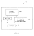
- FIG. 2 shows illustrative circuitry that may be used in device 10.
- device 10 may include control circuitry 26.
- Control circuitry 26 may include storage such as flash memory, hard disk drive memory, solid state storage devices, other nonvolatile memory, random-access memory and other volatile memory, etc.
- Control circuitry 26 may also include processing circuitry.
- the processing circuitry of control circuitry 26 may include digital signal processors, microcontrollers, application specific integrated circuits, microprocessors, power management unit (PMU) circuits, and processing circuitry that is part of other types of integrated circuits.
- PMU power management unit
- Input-output devices 28 may include wireless communications circuits, displays, speakers, microphones, status indicator light-emitting diodes, sensors such as proximity sensors and accelerometers, touch screens, data port circuits coupled to data ports, analog input-output circuits coupled to audio connectors and other analog signal ports, track pads and other pointing devices, etc.
- Battery 30 may be used to supply power to device 10 when device 10 is not connected to a source of alternating current (AC) power.
- Battery 30 may be, for example, a rechargeable lithium polymer battery. When AC power is available, device 10 can be plugged into the AC power source.
- Power regulator circuitry in control circuitry 26 may be used to convert AC power into DC power for powering device 10 and charging battery 30.
- Buttons 14 may be coupled to control circuitry 26.
- the state of each button 14 may be sensed using button biasing and monitoring circuitry in control circuitry 26.
- button biasing and monitoring circuitry in control circuitry 26.
- the high-impedance path that is created by the open button can be detected using circuitry 26.
- the given button is closed, the short circuit path that is created between the terminals of the button can likewise be detected.
- Buttons 14 may include movable button members (e.g., cylindrical or rectangular members of the type shown in FIG. 1 that reciprocate within holes in the sidewalls of housing 12 when actuated by a user). These button members may bear against a switch mechanism such as a mechanism based on a dome switch. With this type of arrangement, a user may open and close the switch by pressing and releasing the button. For example, in a normally opened design, a user may press a button to compress its dome switch and thereby place the dome switch and button in a closed state. Releasing the button will cause the dome switch to return to its open state. Normally closed designs may also be used.
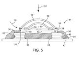
- dome switch 31 may have dome-shaped compressible dome member such as dome member 32. Dome member 32 may be mounted on base 34 and can be compressed when pressed in direction 33.
- Switch (button) terminals 36 may be may be provided on the four corners of dome switch base (housing) 34. In a typical configuration, a first pair of terminals 36 may be electrically connected and may serve as a positive terminal for switch 31 and a second pair of terminals 36 may be electrically connected and may serve as a ground terminal for switch 31. Dome switches with other numbers of terminals may also be used in buttons 14.
- the first dome switch terminal may be electrically connected to an outer dome ring electrode such as outer ring 38 of FIG. 4 .
- the second dome switch terminal may be electrically connected to an inner dome electrode such as inner dome electrode 40 in FIG. 4 .
- a conductive dome structure e.g., a polymer dome with an inner metal layer or a metal dome
- paths 48 and 50 may be used to connect electrodes 38 and 40 of switch 31 to respective switch terminals 36.
- Solder 46 may be used to electrically connect switch terminals 36 to pads 44 on substrate 42 (e.g., a flex circuit).
- underfill material 58 may be used to seal pads 44 and terminals 36. Nevertheless, portions of switch 31 such as the edges of dome member 32 may remain exposed.
- Adhesive 54 may be used to seal the edges of dome member 32 to base 34. The seal that is formed by adhesive 54 may not, however, be perfectly moisture proof. This may allow moisture to enter the interior of dome switch 31 in the vicinity of electrodes (terminals) 38 and 40 along paths such as path 56. When device 10 is not powered, no voltage will appear across terminals 38 and 40. When device 10 is powered, however, the biasing circuits that are used to monitor the state of switch 31 may potentially apply a voltage across terminals 38 and 40. This voltage is typically referred to as being a button bias voltage, because this voltage biases the button terminals so that the state of the button can be detected using monitoring circuitry.
- FIG. 6 A conventional electronic device button biasing and monitoring circuit is shown in FIG. 6 .
- battery power is supplied by battery 62 at battery voltage Vb between ground terminal 64 and voltage regulator 66.
- Voltage regulator 66 may produce a corresponding fixed positive power supply voltage Vcc to positive power supply terminal 70 via path 68.
- Resistor 72 applies voltage Vcc to switch terminal 78 while ground terminal 64 applies ground voltage Vss (0 volts) to switch terminal 80.
- dome switch 76 When dome switch 76 is open, there is an open circuit between terminals 78 and 80.
- switch 76 When switch 76 is closed, there is a short circuit between terminals 78 and 80.
- the state of switch 76 and its associated button is represented by the voltage on terminal 74 and output line 82.
- switch 76 When switch 76 is open, the voltage on line 82 is at a logic high level of Vcc.
- terminals 78 and 80 are shorted together and the voltage on line 82 is a logic low level of Vss
- the problems associated with dendrite formation in conventionally biased buttons can be addressed by controlling the voltage that is applied across terminals 38 and 40 of switch 31 and other such button terminals in device 10. For example, instead of applying a fixed DC voltage, the voltage across terminals 38 and 40 can be pulsed. The average DC voltage level associated with a pulsed bias voltage will be less than the average DC voltage level associated with a fixed bias voltage of the same peak magnitude. As a result, use of bias voltage pulsing schemes can help to reduce the acceleration of dendrite growth that is experience in the presence of non-zero button bias voltages.
- the pulsed bias voltage or a fixed DC bias voltage can be applied selectively.
- the pulsed (or fixed) bias voltage may be applied.
- the biasing circuitry can apply a ground voltage (i.e., a zero-volt bias voltage) or other reduced voltage across the terminals of the button.
- FIG. 7 is a graph showing how a fixed button bias voltage Vcc is applied across terminals 78 and 80 by conventional circuit 84 of FIG. 6 during both periods of time such as time period TA when switch 76 is active and periods of time such as time period TI when switch 76 is inactive.
- circuit 84 needs to use voltage Vcc to monitor the state of switch 76 and produce a corresponding output signal on line 82 that is indicative of the state of switch 76.
- time period TI however, the electronic device containing circuit 84 does not monitor the status of the signal on line 82.
- the state of switch 76 during inactive time period TI is immaterial and does not influence the operation of the electronic device. Applying a fixed voltage Vcc during time period TI therefore needlessly accelerates dendritic growth and increases the likelihood that conventional switch 76 will fail.
- Control circuitry 26 may maintain information on the current operating mode for device 10. For example, control circuitry 26 can determine which software is being run on control circuitry 26 and can determine which device functions are available to a user. In some modes of operation, it may be desirable to have most or all of the buttons of the device available for immediate use by the user. In other modes of operation, however, certain buttons are of little or no use. The states of buttons that are not of present use to the user can therefore be ignored and the bias voltage Vcc that is being applied to those buttons can be grounded or otherwise reduced to minimize dendritic growth.
- Mode-dependent button bias voltage changes can be made by control circuitry 26 in real time, based on the current state of device 10. As different software programs are run on device 10 and/or as a user activates and deactivates various software features, different sets of buttons are needed (and are therefore considered active). The remaining buttons (i.e., the buttons that are not needed or that provide little added user benefit), can be considered inactive buttons and can be biased with modified Vcc profiles. The time-averaged magnitude of bias voltage Vcc can also be reduced for buttons that are active (e.g., by using a pulsed button biasing scheme).
- FIG. 8 shows an illustrative time-varying Vcc profile that may be used when biasing buttons 14.
- Vcc may be maintained at a fixed positive voltage level.
- Vcc may be taken to a reduced voltage level such as ground (e.g., a Vss level of 0 volts).
- FIG. 9 shows an illustrative time-varying Vcc bias voltage in which Vcc includes square wave voltage pulses P during active time period TA and is held at a reduced fixed voltage such as a ground voltage Vss (e.g., 0 volts) during inactive time period TI.
- Vss ground voltage
- the time-averaged magnitude of Vcc during period TA will be reduced (e.g., to average voltage Va of FIG. 9 ) relative to its peak magnitude.
- the magnitude of Va is less than that of the peak Vcc value, so dendritic growth will be reduced relative to a scenario using a fixed bias voltage at the peak voltage level.
- the elimination of non-zero bias voltages during inactive time period TI may further reduce dendritic growth.
- Vcc button bias profile of the type shown in FIG. 10 may be used to bias buttons 14 in device 10.
- Vcc may be pulsed both during active time periods such as time period TA and inactive time periods such as time period TI. Even though Vcc is not taken to ground voltage Vcc during the entirety of inactive time period TI, the time-averaged magnitude of Vcc can be minimized using pulsed biasing.
- Pulses such as pulses P may have a width such as a width greater than 100 ms, less than 100 ms, less than 10 ms, less than 5 ms, less than 2 ms, less than 0.5 ms, etc.
- the time period between adjacent pulses may be less than 50 ms, less than 100 ms, less than 200 ms, greater than 100 ms, greater than 200 ms, 20-200 ms, 1-100 ms, etc.
- the duty cycle of pulses P i.e., the fraction of time that Vcc is high
- Control circuitry 26 may control Vcc to produce a Vcc profile of the type shown in FIG. 8 , of the type shown in FIG. 9 , of the type shown in FIG. 10 , or other suitable time-varying Vcc profiles that minimize dendritic growth.
- FIG. 11 is a circuit diagram of illustrative circuitry that may be used in controlling Vcc and monitoring the status of a button during various modes of device operation.
- control circuitry 26 may receive battery power Vb from battery 30 on battery power supply lines 94A, 94B, and 94C.
- Battery 30 may have an output voltage of about 1 to 4 volts (as an example).
- Battery voltage Vb may be regulated using voltage regulator circuitry before being applied to lines 94A, 94B, and 94C (e.g., using a power management unit that is part of a stand-alone power management integrated circuit or that is part of a larger integrated circuit such as a system-on-chip integrated circuit).
- Control circuit 86 may receive voltage Vb and may use controllable voltage regulator circuitry 88 to produce a time-varying voltage Vcc on output path 94.
- Voltage Vcc may have a peak voltage magnitude of about 0.5 to 3 volts (as an example). Other voltages may be used if desired.
- Voltage Vcc may be routed to resistor 96 or other circuit load element via path 94.
- Input 100 of AND gate 98 may receive voltage Vcc from path 94.
- Resistor 96 may apply voltage Vcc across terminals 36A and 36B of switch 31 and button 14.
- Ground terminals 92 of control circuitry 26 may be maintained at a ground voltage Vss of 0 volts (as an example).
- Circuitry 26 may monitor the state of signal SW_SIG on path 98.
- button 14 When button 14 is open, the path between terminals 36A and 36B will be open circuited. In this situation, signal SW_SIG will track voltage Vcc.
- button 14 When button 14 is closed, terminals 36A and 36B will be shorted together, pulling SW_SIG to ground voltage Vss.
- control circuitry 26 may pulse voltage Vcc, as shown in the graph of FIG. 12 .
- signal SW_SIG will track Vcc, as shown in the graph of FIG. 13 .
- terminal 36A will be connected to ground voltage Vss and SW_SIG will be equal to ground voltage Vss (e.g., 0 volts, as shown in the "closed" period of FIG. 13 ).
- Inverter 100 inverts the signal SW_SIG to produce an inverted version of SW_SIG on input 102 of AND gate 98.
- Gate 98 may produce an output signal CONTROL on output 104 in response to the received values of Vcc on input 100 and the inverted version of SW_SIG on input 102.
- there may be a separate independently controlled biasing circuit for each respective button 14 in device 10 and each biasing circuit may produce a respective CONTROL signal at its output for processing by control circuitry 26.
- CONTROL will generally have a logic low value (e.g., 0 volts) during periods of time in which button 14 is in its open state, because the inputs to AND gate 98 are complements of each other during these periods of time.
- CONTROL will be low until the occurrence of the first Vcc pulse.
- the Vcc pulse is placed on terminal 36A while button 14 is closed, the inverted version of SW_SIG on input 102 will be a constant logic high value.
- the signal CONTROL at the output of AND gate 98 will track the voltage Vcc on input 100 of AND gate 98, as shown in the "closed" period of the trace of FIG. 14 .
- control circuit 86 may hold the value of Vcc high for a given period of time (e.g., a fraction of a second or a few seconds) whenever a low-to-high CONTROL signal transition is detected (see, e.g., dashed line 106 of FIG. 12 and the resulting logic high CONTROL signal of dashed line 106 in FIG. 14 ).
- Control circuitry 26 can debounce the signal CONTROL by ignoring the first portion of the CONTROL pulse (e.g., the first few milliseconds after the rising edge of CONTROL).
- the signal CONTROL reflects button press activity on button 14 and can be used by control circuitry 26 to control the operation of device 10. For example, if circuitry 26 detects that the user of device 10 has pressed an up-volume button, control circuitry 26 can increase the volume of media that is being played back by device 10. If circuitry 26 detects that a menu button has been pressed, control circuitry 26 can display a screen of selectable menu items on display 20, etc.
- the set of buttons that are needed to receive input from the user may change as a function of time. For example, to wake device 10 from sleep, a user may be accustomed to pressing a sleep/wake button (power button) or a menu button. A user may not, however, be expecting that an accidental press of an up or down volume button will wake device 10 from sleep. When device 10 is in a sleep state, it may therefore be necessary to monitor the status of the menu button and the sleep/wake button, but it may not be necessary or desirable to monitor the status of buttons such as up and down volume buttons. When device 10 is operated in other modes, the set of buttons that need to be monitored to receive input from the user may be different.
- buttons 14 may be monitored to ensure that device 10 is fully functional and can receive input from any available button (e.g., a sleep/wake button to place the device to sleep, a menu button, and up/down volume buttons).
- any available button e.g., a sleep/wake button to place the device to sleep, a menu button, and up/down volume buttons.
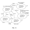
- FIG. 15 is a diagram showing how device 10 may adjust button bias circuits for various buttons (i.e., control circuitry 26 of FIG. 11 ) so that the pattern of bias voltages Vcc that is used in monitoring the buttons changes in various modes.
- control circuitry 26 may provide a fixed, pulsed, or other non-zero bias voltage to all of buttons 14.
- device 10 may adjust the button bias circuits of control circuitry 26 so that fewer buttons are monitored.
- device 10 may be plugged into a wall outlet to receive AC power and thereby charge battery 30 (mode 116).
- mode 116 AC wall power may be converted into DC power using a power converter in device 10. The DC power may be used to charge battery 30 and may be used to power device 10.
- control circuitry 26 can bias and monitor the status of a power button (sometimes referred to as a sleep/wake button), can bias and monitor the status of volume buttons, and can bias and monitor the status of a menu button.
- a power button sometimes referred to as a sleep/wake button
- the bias that is used may be, for example, a fixed voltage (see, e.g., bias Vcc in active time period TA of FIG. 8 ) or a pulsed bias (see, e.g., bias Vcc in region TA of FIG. 9 ).
- control circuitry 26 When battery 30 has become fully charged and a period of inactivity has been detected by control circuitry 26, device 10 may enter mode 114. In mode 114, control circuitry 26 can continue to bias the power and menu buttons (e.g., at a fixed positive voltage or a pulsed voltage), but may apply a voltage of Vss to the button terminals of the volume buttons in device 10. This helps reduce dendritic growth in the volume buttons.
- control circuitry 26 can continue to bias the power and menu buttons (e.g., at a fixed positive voltage or a pulsed voltage), but may apply a voltage of Vss to the button terminals of the volume buttons in device 10. This helps reduce dendritic growth in the volume buttons.
- a user When a user is operating in mode 116 or 114, a user may unplug device 10 from AC power. When this change is detected by circuitry 26, device 10 may transition from mode 116 or 114 to operating mode 108. Device 10 may also transition into operating mode 108 when woken from sleep state 110 or deep sleep state 112. Operating mode 108 may sometimes be referred to as an active mode, normal operating mode, or fully operational mode. In this type of operating mode, most or all of buttons 14 in device 10 may be active. For example, control circuitry 26 may apply a non-zero bias voltage Vcc (fixed or pulsed) to the power button, to the volume buttons, and to the menu button.
- Vcc fixed or pulsed
- control circuitry 26 can detect user button presses on the power button.
- a user may press and hold the power button for a first period of time (e.g., a fraction of a second) to direct circuitry 26 to transition device 10 to a sleep state (mode 110).
- a user may press and hold the power button for a second period of time (e.g., a second or more) to direct circuitry 26 to transition device 10 to a deep sleep state such as mode 112 (e.g., after the user responds to an on-screen confirmation option).
- control circuitry 26 may not need to monitor the status of as many buttons as in mode 110. For example, in modes 110 and 112, control circuitry 26 may only bias and monitor the state of the power button and the menu button. If a long press of the power button is detected during mode 108, control circuitry 26 may place device 10 in deep sleep mode 112 (e.g., after a user responds to an on-screen confirmation option). During sleep mode 110, fewer circuits may be active in device 10 than in active mode 108 to conserve power. Deep sleep mode 112 may involve deactivating more circuitry to conserve additional power relative to sleep mode 110.
- control circuitry 26 can transition device 10 to an active state (mode 108) and can begin biasing and monitoring all buttons 14 (e.g., power, volume, and menu). Because it is not necessary to monitor the status of the volume buttons in modes 110 and 112, control circuitry 26 can deactivate the bias voltage (i.e., Vcc can be held at Vss as shown in inactive time period TI of FIG. 8 ). With bias voltage Vcc at Vss, dendritic growth in the volume buttons may be reduced.
- Device 10 may implement selective button biasing schemes of the type described in connection with FIG. 15 in a device with one to three buttons, in a device with one to five buttons, in a device with two or more buttons, in a device with more than three or more than four buttons, etc.
- the biasing voltages Vcc e.g., a fixed or pulsed voltage Vcc
- the biasing voltages Vcc may be temporarily taken to Vss or other suitable reduced voltage relative to the nominal Vcc maximum level used during normal biasing.
- buttons may be biased by applying pulsed voltages across the terminals of the buttons.
- Voltage bias pulses may be square wave pulses or may have other suitable time-varying signal shapes, may have duty cycles less than 100% to reduce average voltage levels, may have regularly spaced pulses or pulses that are spaced at irregular intervals, or may have other suitable characteristics.
- Modes 108, 110, 112, 114, and 116 of FIG. 15 are merely illustrative examples.
- device 10 may operate in any number of different modes.
- device 10 may implement selective button biasing schemes for one or more buttons.
- Device 10 may implement selective button biasing schemes for buttons in device 10 such as menu keys, sleep keys, volume keys, lock/unlock keys, keypad keys, numeric pad keys, zoom keys, track pad keys, function keys, dedicated or semi-dedicated keys for launching an operating system function, application, or other software, fast forward, reverse, stop, pause, and other media playback keys, home buttons, buttons for controlling telephone calls (e.g., an answer call key, a hold key, a conference call key, etc.), slider switches, rocker switches, multi-position switches, help buttons, etc.
- buttons in device 10 such as menu keys, sleep keys, volume keys, lock/unlock keys, keypad keys, numeric pad keys, zoom keys, track pad keys, function keys, dedicated or semi-dedicated keys for launching an operating system function, application, or other software, fast forward, reverse, stop, pause, and other media playback keys, home buttons, buttons for controlling telephone calls (e.g., an answer call key, a hold key, a conference call key, etc.), slider
- an electronic device includes multiple buttons each of which has button terminals and control circuitry that is configured to apply a fixed non-zero bias voltage across the button terminals of at least first and second buttons in the plurality of buttons during a first mode of operation of the electronic device and that is configured to apply a fixed zero voltage across the button terminals of the first button while applying the fixed non-zero bias voltage across the button terminals of the second button during a second mode of operation of the electronic device.
- the first button includes a volume button.
- the first button includes a menu button.
- the second button includes a sleep/wake button.
- buttons each include a respective dome switch having electrodes coupled to the button terminals of that button.
- circuitry includes a button having first and second button terminals, wherein the button is operable in an open state in which an open circuit is formed between the first and second button terminals and is operable in a closed state in which the first and second button terminals are short circuited together and that includes control circuitry that applies a pulsed bias voltage across the button terminals using a bias voltage path and that determines whether the button is in the open state or the closed state while the pulsed bias voltage is being applied across the button terminals.
- control circuitry includes a logic circuit having a first input that is coupled to the bias voltage path, a second input that is coupled to the first button terminal, and an output at which a corresponding signal is generated representing whether the button is in the open state or the closed state.
- the logic circuit includes an AND gate.
- control circuitry is configured to generate the pulsed bias voltage at a duty cycle of less than 20%.
- control circuitry is configured to generate pulses in the pulsed bias voltage that having pulse widths of less than 10 ms each.
- the circuitry includes additional buttons and the control circuitry is configured to prevent application of the pulsed bias voltage to the button when the electronic device is operating in an operating mode in which input from the button is not monitored while input from the additional buttons is monitored.
- control circuitry is configured to generate square wave pulses in the pulsed bias voltage.
- a method for operating an electronic device that has a plurality of buttons each of which has button terminals and each of which is operable in open and closed positions.
- the method includes operating the electronic device in a first mode in which a non-zero bias voltage is applied across the button terminals of each of the plurality of buttons and operating the electronic device in a second mode in which a bias voltage of zero volts is applied across the button terminals of a first of the plurality of buttons and in which a non-zero bias voltage is applied across the button terminals of a second of the plurality of buttons.
- operating the electronic device in the first mode includes operating the electronic device in a fully operational mode in which activity on each of the plurality of buttons is monitored by control circuitry in the electronic device.
- operating the electronic device in the second mode includes operating the electronic device in a sleep mode in which button press activity on the second of the plurality of buttons is monitored by control circuitry in the electronic device using the non-zero bias voltage and in which button press activity on the first of the plurality of buttons is not monitored.
- the first button comprises a volume button and operating the electronic device in the second mode includes operating the electronic device in a sleep mode without monitoring whether the volume button is in the closed or open position.
- a method of operating an electronic device having a button with button terminals that is movable between open and closed positions includes, with control circuitry, applying a pulsed voltage across the button terminals of the button while monitoring the button using the applied pulsed voltage to determine whether the button is in the open or closed position.
- control circuitry is configured to apply square wave pulses with a duty cycle of less than 20% across the button terminals.
- the method includes monitoring signals on one of the button terminals using a logic circuit that receives the pulsed voltage as an input.
- the electronic device includes an additional button having first and second terminals and monitoring the signals includes monitoring the signals using the pulsed voltage while applying a zero-volt bias voltage across the first and second terminals of the additional button.
Landscapes
- Engineering & Computer Science (AREA)
- Theoretical Computer Science (AREA)
- General Engineering & Computer Science (AREA)
- Human Computer Interaction (AREA)
- Physics & Mathematics (AREA)
- General Physics & Mathematics (AREA)
- Input From Keyboards Or The Like (AREA)
- Push-Button Switches (AREA)
- Telephone Function (AREA)
Abstract
Description
- This application claims priority to United States patent application No.
61/378,899 filed August 31, 2010 13/094,098 filed April 26, 2011 - This relates to electronic devices, such as electronic devices with buttons.
- Electronic devices such as cellular telephones, computers, music players, and other devices often use buttons to gather user input. A typical button may have a movable button member that actuates a switch such as a dome switch. To ensure reliable operation, environmental sealing techniques are sometimes used to prevent moisture from damaging internal components. Despite these measures, dome switches and other button components may still be vulnerable to damage when exposed to moisture. This potential for failure is exacerbated by the use of direct current (DC) button biasing voltages. This is because the DC voltage encourages dendritic growth in the presence of moisture. Dendrites may cause undesirable short circuits and device failures.
- It would therefore be desirable to provide improved button arrangements for electronic devices.
- Dendritic growth in electronic device buttons may be minimized by providing electronic devices with button monitoring circuits that use time-varying bias voltages. During some modes of operation the status of certain buttons may need to be monitored. For example, during normal operation, it may be desirable to monitor the status of a power button, a menu button, and volume buttons. In other modes of operation, such as in a sleep mode, it may not be necessary or desirable to monitor the status of one or more of these buttons. For example, it may be desirable to monitor only the status of the power and menu buttons and not the volume buttons. Because the volume buttons are not being monitored in the sleep state, the non-zero bias voltage that would otherwise be applied to the volume buttons can be replaced with a bias voltage of zero volts.
- Mode-dependent adjustment of the pattern of bias voltages that are applied to the buttons allows unused buttons to be exposed to reduced voltages. This avoids the acceleration of dendritic growth that typically arises in the presence of voltage differences across button terminals when buttons are exposed to moisture.
- The average voltage across the button terminals of active and inactive buttons can be reduced by using pulsed bias voltages. With this type of configuration, the voltage bias that is produced by the voltage bias and monitoring circuitry in the electronic device may be provided in the form of a series of square wave pulses. Logic circuitry may process a signal from one of the button terminals and the pulsed bias voltage to produce a control signal that is responsive to the state of the button.
- Further features of the invention, its nature and various advantages will be more apparent from the accompanying drawings and the following detailed description of the preferred embodiments.
-
-
FIG. 1 is a perspective view of an illustrative electronic device having buttons and button biasing and monitoring circuitry in accordance with an embodiment of the present invention. -
FIG. 2 is a schematic diagram of illustrative circuitry for an electronic device with buttons in accordance with an embodiment of the present invention. -
FIG. 3 is a perspective view of an illustrative dome switch structure of the type that may be used in a button in an electronic device in accordance with an embodiment of the present invention. -
FIG. 4 is a top view of an interior portion of a dome switch showing inner and outer conductive terminals that may be included in the dome switch in accordance with an embodiment of the present invention. -
FIG. 5 is a cross-sectional side view of an illustrative dome switch having a shape of the type shown inFIG. 3 and switch terminals of the type shown inFIG. 4 in accordance with an embodiment of the present invention. -
FIG. 6 is a circuit diagram of a conventional button circuit that uses a fixed button bias voltage to detect button activity from a button. -
FIG. 7 is a graph showing how the button bias voltage of the conventional button circuit ofFIG. 6 is constant as a function of time. -
FIG. 8 is a graph showing how a button bias voltage may be changed as a function of time so that there is a reduced or eliminated button bias voltage during times when a button is not in use in accordance with an embodiment of the present invention. -
FIG. 9 is a graph showing how a button bias may be pulsed during periods of time when a button is active and may be turned off completely during periods of time when the button is inactive in accordance with an embodiment of the present invention. -
FIG. 10 is a graph showing how a button bias may be pulsed during periods of button activity and inactivity in accordance with an embodiment of the present invention. -
FIG. 11 is a circuit diagram of illustrative circuitry that may be used to provide buttons with time-varying bias voltages in accordance with an embodiment of the present invention. -
FIG. 12 is a graph of an illustrative modulated button bias voltage that may be provided using a circuit of the type shown inFIG. 11 in accordance with an embodiment of the present invention. -
FIG. 13 is a graph showing a switch signal that may be produced when a switch is opened and closed while being biased using a bias voltage of the type shown inFIG. 12 in accordance with an embodiment of the present invention. -
FIG. 14 is a graph of an illustrative output control signal representing button status that may be generated using a circuit of the type shown inFIG. 11 in response to button signals of the type shown inFIGS. 12 and 13 . -
FIG. 15 is a diagram showing how button bias voltages for various buttons in an electronic device of the type shown inFIG. 1 may be varied by an electronic device as the electronic device transitions between operating modes in accordance with an embodiment of the present invention. - An illustrative electronic device with buttons is shown in
FIG. 1 . Electronic such asdevice 10 ofFIG. 1 that may be provided with buttons include computers, handheld electronic devices such as cellular telephones and portable music players, portable devices such as tablet computers and laptop computers, gaming devices, and other electronic equipment. As shown in the example ofFIG. 1 ,electronic device 10 may include a housing such ashousing 12.Housing 12 may be formed from plastic, metal, fiber composites such as carbon fiber, glass, ceramic, other materials, and combinations of these materials.Housing 12 may be formed using a unibody construction in whichhousing 12 is formed from an integrated piece of material or may be formed from frame structures, housing walls, and other components that are attached to each other using fasteners, adhesive, and other attachment mechanisms. - A display such as
display 20 may be mounted on the front face of device 10 (as an example).Display 20 may be a touch screen display. If desired, a track pad or other touch sensitive devices, a keyboard, a microphone, a speaker (e.g., a speaker associated with speaker port 18), and other user input-output devices may be used to gather user input and to supply the user with output. Ports such asport 16 may receive mating connectors (e.g., an audio plug, a connector associated with a data cable, etc.). - Buttons such as
buttons 14 may be used to provide a user ofdevice 10 with a way to supplydevice 10 with user input. A user may, for example, press a particular button (e.g., a menu button on the front face of device 10) to directdevice 10 to display a menu of selectable on-screen options (e.g., icons) ondisplay 20. A user may press other buttons to increase or decrease the volume of sound that is being played back to a user through a speaker indevice 10 or through a pair of headphones attached todevice 10 usingport 16. If desired,buttons 14 may include a sleep/wake button (sometimes referred to as a sleep button or a power button) that can be pressed to alternately putdevice 10 into sleep and wake states or that can be held for a longer amount of time to place a device in a deep sleep mode. During sleep state operation, nonessential components may be turned off to conserve power. During wake state operation (sometimes referred to as active mode or normal operating mode), the circuitry ofdevice 10 may be activated for use by a user. -
Other buttons 14 that may be provided indevice 10 include keypad keys, numeric pad keys, zoom keys, track pad keys, function keys, dedicated or semi-dedicated keys for launching an operating system function, application, or other software, fast forward, reverse, stop, pause, and other media playback keys, home buttons, buttons for controlling telephone calls (e.g., an answer call key, a hold key, a conference call key, etc.), slider switches, rocker switches, multi-position switches, help buttons, etc. In general,buttons 14 may be formed using any suitable mechanism that can open and close or otherwise alter a circuit. Examples wherebuttons 14 are implemented as momentary buttons using dome switches are sometimes described herein as an example. This is, however, merely illustrative. -
FIG. 2 shows illustrative circuitry that may be used indevice 10. As shown inFIG. 2 ,device 10 may includecontrol circuitry 26.Control circuitry 26 may include storage such as flash memory, hard disk drive memory, solid state storage devices, other nonvolatile memory, random-access memory and other volatile memory, etc.Control circuitry 26 may also include processing circuitry. the processing circuitry ofcontrol circuitry 26 may include digital signal processors, microcontrollers, application specific integrated circuits, microprocessors, power management unit (PMU) circuits, and processing circuitry that is part of other types of integrated circuits. - Input-
output devices 28 may include wireless communications circuits, displays, speakers, microphones, status indicator light-emitting diodes, sensors such as proximity sensors and accelerometers, touch screens, data port circuits coupled to data ports, analog input-output circuits coupled to audio connectors and other analog signal ports, track pads and other pointing devices, etc. -
Battery 30 may be used to supply power todevice 10 whendevice 10 is not connected to a source of alternating current (AC) power.Battery 30 may be, for example, a rechargeable lithium polymer battery. When AC power is available,device 10 can be plugged into the AC power source. Power regulator circuitry incontrol circuitry 26 may be used to convert AC power into DC power for poweringdevice 10 and chargingbattery 30. -
Buttons 14 may be coupled to controlcircuitry 26. The state of eachbutton 14 may be sensed using button biasing and monitoring circuitry incontrol circuitry 26. When, for example, a given button is open, the high-impedance path that is created by the open button can be detected usingcircuitry 26. When the given button is closed, the short circuit path that is created between the terminals of the button can likewise be detected. -
Buttons 14 may include movable button members (e.g., cylindrical or rectangular members of the type shown inFIG. 1 that reciprocate within holes in the sidewalls ofhousing 12 when actuated by a user). These button members may bear against a switch mechanism such as a mechanism based on a dome switch. With this type of arrangement, a user may open and close the switch by pressing and releasing the button. For example, in a normally opened design, a user may press a button to compress its dome switch and thereby place the dome switch and button in a closed state. Releasing the button will cause the dome switch to return to its open state. Normally closed designs may also be used. - An illustrative dome switch of the type that may be used in
buttons 14 ofFIG. 1 is shown inFIG. 3 . As shown inFIG. 3 ,dome switch 31 may have dome-shaped compressible dome member such asdome member 32.Dome member 32 may be mounted onbase 34 and can be compressed when pressed indirection 33. Switch (button)terminals 36 may be may be provided on the four corners of dome switch base (housing) 34. In a typical configuration, a first pair ofterminals 36 may be electrically connected and may serve as a positive terminal forswitch 31 and a second pair ofterminals 36 may be electrically connected and may serve as a ground terminal forswitch 31. Dome switches with other numbers of terminals may also be used inbuttons 14. - The first dome switch terminal may be electrically connected to an outer dome ring electrode such as
outer ring 38 ofFIG. 4 . The second dome switch terminal may be electrically connected to an inner dome electrode such asinner dome electrode 40 inFIG. 4 . Whendome member 32 is compressed, a conductive dome structure (e.g., a polymer dome with an inner metal layer or a metal dome) that is withindome member 32 such asdome structure 52 ofFIG. 5 may be compressed and may form a short circuit path betweenelectrodes FIG. 5 ,paths electrodes switch 31 torespective switch terminals 36.Solder 46 may be used to electrically connectswitch terminals 36 topads 44 on substrate 42 (e.g., a flex circuit). Whendome member 32 is compressed in direction 33 (e.g., by a button member associated with the button in which dome switch 31 is mounted),dome structure 52 willshort terminals switch 31. - To help reduce the impact of exposure to moisture,
underfill material 58 may be used to sealpads 44 andterminals 36. Nevertheless, portions ofswitch 31 such as the edges ofdome member 32 may remain exposed.Adhesive 54 may be used to seal the edges ofdome member 32 tobase 34. The seal that is formed by adhesive 54 may not, however, be perfectly moisture proof. This may allow moisture to enter the interior ofdome switch 31 in the vicinity of electrodes (terminals) 38 and 40 along paths such aspath 56. Whendevice 10 is not powered, no voltage will appear acrossterminals device 10 is powered, however, the biasing circuits that are used to monitor the state ofswitch 31 may potentially apply a voltage acrossterminals - A conventional electronic device button biasing and monitoring circuit is shown in
FIG. 6 . As shown in circuit 84 ofFIG. 6 , battery power is supplied bybattery 62 at battery voltage Vb betweenground terminal 64 andvoltage regulator 66.Voltage regulator 66 may produce a corresponding fixed positive power supply voltage Vcc to positivepower supply terminal 70 viapath 68.Resistor 72 applies voltage Vcc to switch terminal 78 whileground terminal 64 applies ground voltage Vss (0 volts) to switchterminal 80. When dome switch 76 is open, there is an open circuit betweenterminals switch 76 is closed, there is a short circuit betweenterminals switch 76 and its associated button is represented by the voltage on terminal 74 andoutput line 82. Whenswitch 76 is open, the voltage online 82 is at a logic high level of Vcc. Whenswitch 76 is closed,terminals line 82 is a logic low level of Vss. - The continuous application of the constant Vcc voltage of circuit 84 across
terminals switch 76. This can causeswitch 76 to develop a permanent short circuit. Failures of this type may render a cellular telephone or otherdevice containing switch 76 inoperable. - The problems associated with dendrite formation in conventionally biased buttons can be addressed by controlling the voltage that is applied across
terminals switch 31 and other such button terminals indevice 10. For example, instead of applying a fixed DC voltage, the voltage acrossterminals - If desired, the pulsed bias voltage or a fixed DC bias voltage can be applied selectively. During periods of time in which a given button is active, the pulsed (or fixed) bias voltage may be applied. During periods of time in which the given button is inactive (i.e., when
device 10 is operating in a mode in which the state of the given button is immaterial and is not being monitored), the biasing circuitry can apply a ground voltage (i.e., a zero-volt bias voltage) or other reduced voltage across the terminals of the button. -
FIG. 7 is a graph showing how a fixed button bias voltage Vcc is applied acrossterminals FIG. 6 during both periods of time such as time period TA whenswitch 76 is active and periods of time such as time period TI whenswitch 76 is inactive. During time period TA, circuit 84 needs to use voltage Vcc to monitor the state ofswitch 76 and produce a corresponding output signal online 82 that is indicative of the state ofswitch 76. During time period TI, however, the electronic device containing circuit 84 does not monitor the status of the signal online 82. The state ofswitch 76 during inactive time period TI is immaterial and does not influence the operation of the electronic device. Applying a fixed voltage Vcc during time period TI therefore needlessly accelerates dendritic growth and increases the likelihood thatconventional switch 76 will fail. - Reductions to the time-averaged magnitude of the bias voltage Vcc can be made by pulsing Vcc and/or by taking Vcc to ground or other reduced voltage during certain periods of time. Control circuitry 26 (
FIG. 2 ) may maintain information on the current operating mode fordevice 10. For example,control circuitry 26 can determine which software is being run oncontrol circuitry 26 and can determine which device functions are available to a user. In some modes of operation, it may be desirable to have most or all of the buttons of the device available for immediate use by the user. In other modes of operation, however, certain buttons are of little or no use. The states of buttons that are not of present use to the user can therefore be ignored and the bias voltage Vcc that is being applied to those buttons can be grounded or otherwise reduced to minimize dendritic growth. - Mode-dependent button bias voltage changes can be made by
control circuitry 26 in real time, based on the current state ofdevice 10. As different software programs are run ondevice 10 and/or as a user activates and deactivates various software features, different sets of buttons are needed (and are therefore considered active). The remaining buttons (i.e., the buttons that are not needed or that provide little added user benefit), can be considered inactive buttons and can be biased with modified Vcc profiles. The time-averaged magnitude of bias voltage Vcc can also be reduced for buttons that are active (e.g., by using a pulsed button biasing scheme). -
FIG. 8 shows an illustrative time-varying Vcc profile that may be used when biasingbuttons 14. During time periods such as TA in which a button is active, Vcc may be maintained at a fixed positive voltage level. During time periods such as TI in which a button is not active (i.e., when it is considered impossible or unlikely that the button will be pressed by the user to supply user input todevice 10 or when it is otherwise desired to ignore presses of the button), Vcc may be taken to a reduced voltage level such as ground (e.g., a Vss level of 0 volts). -
FIG. 9 shows an illustrative time-varying Vcc bias voltage in which Vcc includes square wave voltage pulses P during active time period TA and is held at a reduced fixed voltage such as a ground voltage Vss (e.g., 0 volts) during inactive time period TI. Due to the pulsed nature of the Vcc profile during active period TA, the time-averaged magnitude of Vcc during period TA will be reduced (e.g., to average voltage Va ofFIG. 9 ) relative to its peak magnitude. The magnitude of Va is less than that of the peak Vcc value, so dendritic growth will be reduced relative to a scenario using a fixed bias voltage at the peak voltage level. The elimination of non-zero bias voltages during inactive time period TI may further reduce dendritic growth. - If desired, a time-varying Vcc button bias profile of the type shown in
FIG. 10 may be used to biasbuttons 14 indevice 10. In the arrangement ofFIG. 10 , Vcc may be pulsed both during active time periods such as time period TA and inactive time periods such as time period TI. Even though Vcc is not taken to ground voltage Vcc during the entirety of inactive time period TI, the time-averaged magnitude of Vcc can be minimized using pulsed biasing. - Pulses such as pulses P may have a width such as a width greater than 100 ms, less than 100 ms, less than 10 ms, less than 5 ms, less than 2 ms, less than 0.5 ms, etc. The time period between adjacent pulses may be less than 50 ms, less than 100 ms, less than 200 ms, greater than 100 ms, greater than 200 ms, 20-200 ms, 1-100 ms, etc. The duty cycle of pulses P (i.e., the fraction of time that Vcc is high) may be greater than 75%, less than 75%, less than 50%, less than 20%, less than 10%, or less than 5% (as examples).
-
Control circuitry 26 may control Vcc to produce a Vcc profile of the type shown inFIG. 8 , of the type shown inFIG. 9 , of the type shown inFIG. 10 , or other suitable time-varying Vcc profiles that minimize dendritic growth. -
FIG. 11 is a circuit diagram of illustrative circuitry that may be used in controlling Vcc and monitoring the status of a button during various modes of device operation. As shown inFIG. 11 ,control circuitry 26 may receive battery power Vb frombattery 30 on batterypower supply lines Battery 30 may have an output voltage of about 1 to 4 volts (as an example). Battery voltage Vb may be regulated using voltage regulator circuitry before being applied tolines Control circuit 86 may receive voltage Vb and may use controllablevoltage regulator circuitry 88 to produce a time-varying voltage Vcc onoutput path 94. Voltage Vcc may have a peak voltage magnitude of about 0.5 to 3 volts (as an example). Other voltages may be used if desired. - Voltage Vcc may be routed to
resistor 96 or other circuit load element viapath 94. Input 100 of ANDgate 98 may receive voltage Vcc frompath 94.Resistor 96 may apply voltage Vcc acrossterminals switch 31 andbutton 14.Ground terminals 92 ofcontrol circuitry 26 may be maintained at a ground voltage Vss of 0 volts (as an example). -
Circuitry 26 may monitor the state of signal SW_SIG onpath 98. Whenbutton 14 is open, the path betweenterminals button 14 is closed,terminals - Using
voltage regulator 88 incontrol circuit 86,control circuitry 26 may pulse voltage Vcc, as shown in the graph ofFIG. 12 . During times in whichbutton 14 is open, signal SW_SIG will track Vcc, as shown in the graph ofFIG. 13 . During times in whichbutton 14 is closed, terminal 36A will be connected to ground voltage Vss and SW_SIG will be equal to ground voltage Vss (e.g., 0 volts, as shown in the "closed" period ofFIG. 13 ). -
Inverter 100 inverts the signal SW_SIG to produce an inverted version of SW_SIG oninput 102 of ANDgate 98.Gate 98 may produce an output signal CONTROL onoutput 104 in response to the received values of Vcc oninput 100 and the inverted version of SW_SIG oninput 102. As indicated bydots 105, there may be a separate independently controlled biasing circuit for eachrespective button 14 indevice 10 and each biasing circuit may produce a respective CONTROL signal at its output for processing bycontrol circuitry 26. - As shown in
FIG. 14 , CONTROL will generally have a logic low value (e.g., 0 volts) during periods of time in whichbutton 14 is in its open state, because the inputs to ANDgate 98 are complements of each other during these periods of time. Whenbutton 14 is in its closed state, CONTROL will be low until the occurrence of the first Vcc pulse. When the Vcc pulse is placed on terminal 36A whilebutton 14 is closed, the inverted version of SW_SIG oninput 102 will be a constant logic high value. As a result, the signal CONTROL at the output of ANDgate 98 will track the voltage Vcc oninput 100 of ANDgate 98, as shown in the "closed" period of the trace ofFIG. 14 . - If desired,
control circuit 86 may hold the value of Vcc high for a given period of time (e.g., a fraction of a second or a few seconds) whenever a low-to-high CONTROL signal transition is detected (see, e.g., dashedline 106 ofFIG. 12 and the resulting logic high CONTROL signal of dashedline 106 inFIG. 14 ).Control circuitry 26 can debounce the signal CONTROL by ignoring the first portion of the CONTROL pulse (e.g., the first few milliseconds after the rising edge of CONTROL). - The signal CONTROL reflects button press activity on
button 14 and can be used bycontrol circuitry 26 to control the operation ofdevice 10. For example, ifcircuitry 26 detects that the user ofdevice 10 has pressed an up-volume button,control circuitry 26 can increase the volume of media that is being played back bydevice 10. Ifcircuitry 26 detects that a menu button has been pressed,control circuitry 26 can display a screen of selectable menu items ondisplay 20, etc. - During use of
device 10, the set of buttons that are needed to receive input from the user may change as a function of time. For example, to wakedevice 10 from sleep, a user may be accustomed to pressing a sleep/wake button (power button) or a menu button. A user may not, however, be expecting that an accidental press of an up or down volume button will wakedevice 10 from sleep. Whendevice 10 is in a sleep state, it may therefore be necessary to monitor the status of the menu button and the sleep/wake button, but it may not be necessary or desirable to monitor the status of buttons such as up and down volume buttons. Whendevice 10 is operated in other modes, the set of buttons that need to be monitored to receive input from the user may be different. When, for example,device 10 is being operated in a fully active mode, all ofbuttons 14 may be monitored to ensure thatdevice 10 is fully functional and can receive input from any available button (e.g., a sleep/wake button to place the device to sleep, a menu button, and up/down volume buttons). -
FIG. 15 is a diagram showing howdevice 10 may adjust button bias circuits for various buttons (i.e.,control circuitry 26 ofFIG. 11 ) so that the pattern of bias voltages Vcc that is used in monitoring the buttons changes in various modes. In some modes, such as modes in whichdevice 10 is fully activated (e.g.,mode 108 ofFIG. 15 )control circuitry 26 may provide a fixed, pulsed, or other non-zero bias voltage to all ofbuttons 14. In other modes, such as whendevice 10 is in sleep mode (e.g.,mode 110 ofFIG. 15 ),device 10 may adjust the button bias circuits ofcontrol circuitry 26 so that fewer buttons are monitored. By applying non-zero bias voltages to only a subset of buttons in certain situations, bias-voltage-dependent dendritic grown in the unbiased buttons can be reduced. - As shown in
FIG. 15 ,device 10 may be plugged into a wall outlet to receive AC power and thereby charge battery 30 (mode 116). Inmode 116, AC wall power may be converted into DC power using a power converter indevice 10. The DC power may be used to chargebattery 30 and may be used topower device 10. In modes such as mode 116 (e.g., modes in whichdevice 10 is attached to a wall outlet and is charging battery 30),control circuitry 26 can bias and monitor the status of a power button (sometimes referred to as a sleep/wake button), can bias and monitor the status of volume buttons, and can bias and monitor the status of a menu button. The bias that is used may be, for example, a fixed voltage (see, e.g., bias Vcc in active time period TA ofFIG. 8 ) or a pulsed bias (see, e.g., bias Vcc in region TA ofFIG. 9 ). - When
battery 30 has become fully charged and a period of inactivity has been detected bycontrol circuitry 26,device 10 may entermode 114. Inmode 114,control circuitry 26 can continue to bias the power and menu buttons (e.g., at a fixed positive voltage or a pulsed voltage), but may apply a voltage of Vss to the button terminals of the volume buttons indevice 10. This helps reduce dendritic growth in the volume buttons. - When a user is operating in
mode device 10 from AC power. When this change is detected bycircuitry 26,device 10 may transition frommode mode 108.Device 10 may also transition intooperating mode 108 when woken fromsleep state 110 ordeep sleep state 112.Operating mode 108 may sometimes be referred to as an active mode, normal operating mode, or fully operational mode. In this type of operating mode, most or all ofbuttons 14 indevice 10 may be active. For example,control circuitry 26 may apply a non-zero bias voltage Vcc (fixed or pulsed) to the power button, to the volume buttons, and to the menu button. Whendevice 10 is operating inmode 108, a user may plugdevice 10 into AC power and, when this change is detected bycircuitry 26,device 10 may transition frommode 108 tomode 116. - Because the power button is active in
mode 108,control circuitry 26 can detect user button presses on the power button. With one suitable arrangement, a user may press and hold the power button for a first period of time (e.g., a fraction of a second) to directcircuitry 26 to transitiondevice 10 to a sleep state (mode 110). A user may press and hold the power button for a second period of time (e.g., a second or more) todirect circuitry 26 to transitiondevice 10 to a deep sleep state such as mode 112 (e.g., after the user responds to an on-screen confirmation option). - In
modes control circuitry 26 may not need to monitor the status of as many buttons as inmode 110. For example, inmodes control circuitry 26 may only bias and monitor the state of the power button and the menu button. If a long press of the power button is detected duringmode 108,control circuitry 26 may placedevice 10 in deep sleep mode 112 (e.g., after a user responds to an on-screen confirmation option). Duringsleep mode 110, fewer circuits may be active indevice 10 than inactive mode 108 to conserve power.Deep sleep mode 112 may involve deactivating more circuitry to conserve additional power relative tosleep mode 110. - If activity on either the power or menu button is detected when
device 10 is inmode 110 ormode 112,control circuitry 26 can transitiondevice 10 to an active state (mode 108) and can begin biasing and monitoring all buttons 14 (e.g., power, volume, and menu). Because it is not necessary to monitor the status of the volume buttons inmodes control circuitry 26 can deactivate the bias voltage (i.e., Vcc can be held at Vss as shown in inactive time period TI ofFIG. 8 ). With bias voltage Vcc at Vss, dendritic growth in the volume buttons may be reduced. -
Device 10 may implement selective button biasing schemes of the type described in connection withFIG. 15 in a device with one to three buttons, in a device with one to five buttons, in a device with two or more buttons, in a device with more than three or more than four buttons, etc. Whenever a mode of operation is entered that does not involve the monitoring of a button or buttons, the biasing voltages Vcc (e.g., a fixed or pulsed voltage Vcc) for those buttons may be temporarily taken to Vss or other suitable reduced voltage relative to the nominal Vcc maximum level used during normal biasing. - In conjunction with a button biasing scheme that adjusts which buttons are biased depending on its current operating mode or as part of a button biasing scheme in which buttons are biased substantially equally during both active and inactive periods, buttons may be biased by applying pulsed voltages across the terminals of the buttons. Voltage bias pulses may be square wave pulses or may have other suitable time-varying signal shapes, may have duty cycles less than 100% to reduce average voltage levels, may have regularly spaced pulses or pulses that are spaced at irregular intervals, or may have other suitable characteristics.
-
Modes FIG. 15 are merely illustrative examples. In general,device 10 may operate in any number of different modes. In some of the modes ofdevice 10,device 10 may implement selective button biasing schemes for one or more buttons.Device 10 may implement selective button biasing schemes for buttons indevice 10 such as menu keys, sleep keys, volume keys, lock/unlock keys, keypad keys, numeric pad keys, zoom keys, track pad keys, function keys, dedicated or semi-dedicated keys for launching an operating system function, application, or other software, fast forward, reverse, stop, pause, and other media playback keys, home buttons, buttons for controlling telephone calls (e.g., an answer call key, a hold key, a conference call key, etc.), slider switches, rocker switches, multi-position switches, help buttons, etc. - In accordance with an embodiment, an electronic device is provided that includes multiple buttons each of which has button terminals and control circuitry that is configured to apply a fixed non-zero bias voltage across the button terminals of at least first and second buttons in the plurality of buttons during a first mode of operation of the electronic device and that is configured to apply a fixed zero voltage across the button terminals of the first button while applying the fixed non-zero bias voltage across the button terminals of the second button during a second mode of operation of the electronic device.
- In accordance with another embodiment, the first button includes a volume button.
- In accordance with another embodiment, the first button includes a menu button.
- In accordance with another embodiment, the second button includes a sleep/wake button.
- In accordance with another embodiment, the buttons each include a respective dome switch having electrodes coupled to the button terminals of that button.
- In accordance with an embodiment, circuitry is provided that includes a button having first and second button terminals, wherein the button is operable in an open state in which an open circuit is formed between the first and second button terminals and is operable in a closed state in which the first and second button terminals are short circuited together and that includes control circuitry that applies a pulsed bias voltage across the button terminals using a bias voltage path and that determines whether the button is in the open state or the closed state while the pulsed bias voltage is being applied across the button terminals.
- In accordance with another embodiment, the control circuitry includes a logic circuit having a first input that is coupled to the bias voltage path, a second input that is coupled to the first button terminal, and an output at which a corresponding signal is generated representing whether the button is in the open state or the closed state.
- In accordance with another embodiment, the logic circuit includes an AND gate.
- In accordance with another embodiment, the control circuitry is configured to generate the pulsed bias voltage at a duty cycle of less than 20%.
- In accordance with another embodiment, the control circuitry is configured to generate pulses in the pulsed bias voltage that having pulse widths of less than 10 ms each.
- In accordance with another embodiment, the circuitry includes additional buttons and the control circuitry is configured to prevent application of the pulsed bias voltage to the button when the electronic device is operating in an operating mode in which input from the button is not monitored while input from the additional buttons is monitored.
- In accordance with another embodiment, the control circuitry is configured to generate square wave pulses in the pulsed bias voltage.
- In accordance with an embodiment, a method is provided for operating an electronic device that has a plurality of buttons each of which has button terminals and each of which is operable in open and closed positions. The method includes operating the electronic device in a first mode in which a non-zero bias voltage is applied across the button terminals of each of the plurality of buttons and operating the electronic device in a second mode in which a bias voltage of zero volts is applied across the button terminals of a first of the plurality of buttons and in which a non-zero bias voltage is applied across the button terminals of a second of the plurality of buttons.
- In accordance with another embodiment, operating the electronic device in the first mode includes operating the electronic device in a fully operational mode in which activity on each of the plurality of buttons is monitored by control circuitry in the electronic device.
- In accordance with another embodiment, operating the electronic device in the second mode includes operating the electronic device in a sleep mode in which button press activity on the second of the plurality of buttons is monitored by control circuitry in the electronic device using the non-zero bias voltage and in which button press activity on the first of the plurality of buttons is not monitored.
- In accordance with another embodiment, the first button comprises a volume button and operating the electronic device in the second mode includes operating the electronic device in a sleep mode without monitoring whether the volume button is in the closed or open position.
- In accordance with an embodiment, a method of operating an electronic device having a button with button terminals that is movable between open and closed positions is provided that includes, with control circuitry, applying a pulsed voltage across the button terminals of the button while monitoring the button using the applied pulsed voltage to determine whether the button is in the open or closed position.
- In accordance with another embodiment, the control circuitry is configured to apply square wave pulses with a duty cycle of less than 20% across the button terminals.
- In accordance with another embodiment, the method includes monitoring signals on one of the button terminals using a logic circuit that receives the pulsed voltage as an input.
- In accordance with another embodiment, the electronic device includes an additional button having first and second terminals and monitoring the signals includes monitoring the signals using the pulsed voltage while applying a zero-volt bias voltage across the first and second terminals of the additional button.
- The foregoing is merely illustrative of the principles of this invention and various modifications can be made by those skilled in the art without departing from the scope and spirit of the invention.
Claims (12)
- An electronic device, comprising:a plurality of buttons each of which has button terminals; andcontrol circuitry that is configured to apply a fixed non-zero bias voltage across the button terminals of at least first and second buttons in the plurality of buttons during a first mode of operation of the electronic device and that is configured to apply a fixed zero voltage across the button terminals of the first button while applying the fixed non-zero bias voltage across the button terminals of the second button during a second mode of operation of the electronic device.
- The electronic device defined in claim 1 wherein the first button comprises a volume button.
- The electronic device defined in claim 1 wherein the second button comprises a menu button.
- The electronic device defined in claim 2 wherein the second button comprises a sleep/wake button.
- The electronic device defined in claim 1 wherein the buttons each include a respective dome switch having electrodes coupled to the button terminals of that button.
- A method for operating an electronic device that has a plurality of buttons each of which has button terminals and each of which is operable in open and closed positions, the method comprising:operating the electronic device in a first mode in which a non-zero bias voltage is applied across the button terminals of each of the plurality of buttons; andoperating the electronic device in a second mode in which a bias voltage of zero volts is applied across the button terminals of a first of the plurality of buttons and in which a non-zero bias voltage is applied across the button terminals of a second of the plurality of buttons.
- The method defined in claim 6 wherein operating the electronic device in the first mode comprises operating the electronic device in a fully operational mode in which activity on each of the plurality of buttons is monitored by control circuitry in the electronic device.
- The method defined in claim 7 wherein operating the electronic device in the second mode comprises operating the electronic device in a sleep mode in which button press activity on the second of the plurality of buttons is monitored by control circuitry in the electronic device using the non-zero bias voltage and in which button press activity on the first of the plurality of buttons is not monitored.
- The method defined in claim 6 wherein the first button comprises a volume button and wherein operating the electronic device in the second mode comprises operating the electronic device in a sleep mode without monitoring whether the volume button is in the closed or open position.
- The method defined in claim 6 wherein applying the non-zero bias voltage across the button terminals of each of the plurality of buttons comprises:with control circuitry, applying a pulsed voltage across the button terminals of that button while monitoring that button using the applied pulsed voltage to determine whether that button is in the open or closed position.
- The method defined in claim 10 wherein the control circuitry is configured to apply square wave pulses with a duty cycle of less than 20% across the button terminals of that button.
- The method defined in claim 10 further comprising:monitoring signals on one of the button terminals of that button using a logic circuit that receives the pulsed voltage as an input.
Applications Claiming Priority (2)
| Application Number | Priority Date | Filing Date | Title |
|---|---|---|---|
| US37889910P | 2010-08-31 | 2010-08-31 | |
| US13/094,098 US8736115B2 (en) | 2010-08-31 | 2011-04-26 | Buttons with modulated bias voltages |
Publications (2)
| Publication Number | Publication Date |
|---|---|
| EP2424118A1 true EP2424118A1 (en) | 2012-02-29 |
| EP2424118B1 EP2424118B1 (en) | 2014-04-09 |
Family
ID=44772727
Family Applications (1)
| Application Number | Title | Priority Date | Filing Date |
|---|---|---|---|
| EP20110178118 Not-in-force EP2424118B1 (en) | 2010-08-31 | 2011-08-19 | Buttons with modulated bias voltages |
Country Status (5)
| Country | Link |
|---|---|
| US (1) | US8736115B2 (en) |
| EP (1) | EP2424118B1 (en) |
| KR (1) | KR101533896B1 (en) |
| CN (1) | CN103154855B (en) |
| WO (1) | WO2012030599A1 (en) |
Families Citing this family (2)
| Publication number | Priority date | Publication date | Assignee | Title |
|---|---|---|---|---|
| KR20150019805A (en) * | 2013-08-16 | 2015-02-25 | 삼성전자주식회사 | Controlling Method For Input Status and Electronic Device supporting the same |
| CN119248116A (en) * | 2023-07-03 | 2025-01-03 | 荣耀终端有限公司 | Level setting method and electronic equipment |
Citations (3)
| Publication number | Priority date | Publication date | Assignee | Title |
|---|---|---|---|---|
| WO1997032426A1 (en) * | 1996-03-01 | 1997-09-04 | Telefonaktiebolaget Lm Ericsson (Publ) | A method and arrangement relating to mobile telephone terminals |
| WO2001095499A1 (en) * | 2000-06-02 | 2001-12-13 | Thomson Licensing S.A. | Apparatus and method for reducing electromigration |
| US20090272639A1 (en) * | 2008-05-01 | 2009-11-05 | Mittleman Adam D | Button assembly with inverted dome switch |
Family Cites Families (9)
| Publication number | Priority date | Publication date | Assignee | Title |
|---|---|---|---|---|
| EP0263652B1 (en) | 1986-10-06 | 1993-03-10 | Brother Kogyo Kabushiki Kaisha | Input device |
| US5990868A (en) | 1997-04-01 | 1999-11-23 | Compaq Computer Corp. | Method and apparatus for performing power conservation in a pointing device located on a wireless data entry device |
| US6622025B2 (en) | 2001-09-28 | 2003-09-16 | Motorola, Inc. | Method and apparatus for entering numbers |
| US7158056B2 (en) | 2004-07-08 | 2007-01-02 | Cypress Semiconductor Corporation | Method and apparatus for scanning a key or button matrix |
| US7834634B2 (en) | 2005-05-06 | 2010-11-16 | Agere Systems Inc. | Low-power switch state detection circuit and method and mobile telephone incorporating the same |
| KR100877067B1 (en) | 2006-01-03 | 2009-01-07 | 삼성전자주식회사 | Haptic Buttons and Haptic Devices Using the Same |
| US7983722B2 (en) | 2007-03-29 | 2011-07-19 | Research In Motion Limited | Headset with multi-button control for a mobile communication device |
| US8063625B2 (en) | 2008-06-18 | 2011-11-22 | Apple Inc. | Momentarily enabled electronic device |
| US8760273B2 (en) | 2008-12-16 | 2014-06-24 | Dell Products, Lp | Apparatus and methods for mounting haptics actuation circuitry in keyboards |
-
2011
- 2011-04-26 US US13/094,098 patent/US8736115B2/en not_active Expired - Fee Related
- 2011-08-19 EP EP20110178118 patent/EP2424118B1/en not_active Not-in-force
- 2011-08-24 CN CN201180049077.2A patent/CN103154855B/en not_active Expired - Fee Related
- 2011-08-24 WO PCT/US2011/049015 patent/WO2012030599A1/en not_active Ceased
- 2011-08-24 KR KR1020137008219A patent/KR101533896B1/en not_active Expired - Fee Related
Patent Citations (3)
| Publication number | Priority date | Publication date | Assignee | Title |
|---|---|---|---|---|
| WO1997032426A1 (en) * | 1996-03-01 | 1997-09-04 | Telefonaktiebolaget Lm Ericsson (Publ) | A method and arrangement relating to mobile telephone terminals |
| WO2001095499A1 (en) * | 2000-06-02 | 2001-12-13 | Thomson Licensing S.A. | Apparatus and method for reducing electromigration |
| US20090272639A1 (en) * | 2008-05-01 | 2009-11-05 | Mittleman Adam D | Button assembly with inverted dome switch |
Also Published As
| Publication number | Publication date |
|---|---|
| CN103154855B (en) | 2016-02-03 |
| US8736115B2 (en) | 2014-05-27 |
| EP2424118B1 (en) | 2014-04-09 |
| KR101533896B1 (en) | 2015-07-03 |
| CN103154855A (en) | 2013-06-12 |
| HK1167755A1 (en) | 2012-12-07 |
| KR20130054400A (en) | 2013-05-24 |
| US20120050964A1 (en) | 2012-03-01 |
| WO2012030599A1 (en) | 2012-03-08 |
Similar Documents
| Publication | Publication Date | Title |
|---|---|---|
| EP2802974B1 (en) | Touch screen device with surface switch | |
| US8319488B2 (en) | Momentarily enabled electronic device | |
| US8396509B2 (en) | Signal transmission path selection circuit and method, and electronic device employing the circuit | |
| US20090307511A1 (en) | Portable electronic devices with power management capabilities | |
| US20100004936A1 (en) | Audio output apparatus capable of suppressing pop noise | |
| HK1046750A1 (en) | A portable telephone and a method of switching power on | |
| US20100158270A1 (en) | Audio Output Apparatus Capable Of Suppressing Pop Noise | |
| EP2424118B1 (en) | Buttons with modulated bias voltages | |
| HK1167755B (en) | Buttons with modulated bias voltages | |
| JP3738245B2 (en) | Power supply for arithmetic unit having low-voltage operation mode and method for controlling power supply to the arithmetic unit | |
| US7834634B2 (en) | Low-power switch state detection circuit and method and mobile telephone incorporating the same | |
| WO2008041064A2 (en) | Detection circuit for detecting the connection of an accessory to a mobile device and method thereof | |
| US10104479B2 (en) | Method for operating a hearing device and a hearing device optimized for being powered by a mercury-free battery | |
| CN217363166U (en) | Control circuit and shooting equipment | |
| CN101621280A (en) | Audio output device for preventing pop sound | |
| US20140071111A1 (en) | Reduction of contention between driver circuitry | |
| EP3112981A1 (en) | Power supply control mechanism, electronic device including the same, hearing aid, and power supply control method | |
| JP2006149132A (en) | Momentary interruption resetting circuit | |
| CN217443770U (en) | Switch control circuit and electronic equipment | |
| CN1930752B (en) | Electronic device and charging connector arrangement | |
| US8279209B2 (en) | Circuit for driving light-emitting element, and cellular phone | |
| CN117041850A (en) | Hole blocking prompting method for electronic equipment and microphone | |
| CN121693831A (en) | Retaining system and method for providing improved retention of a first device to a second device | |
| KR20220154781A (en) | Detection and protection of short circuits between power supplies in Y-bridge drivers | |
| JP2000250787A (en) | Method for monitoring output value level of electronic equipment and personal computer |
Legal Events
| Date | Code | Title | Description |
|---|---|---|---|
| 17P | Request for examination filed |
Effective date: 20110819 |
|
| AK | Designated contracting states |
Kind code of ref document: A1 Designated state(s): AL AT BE BG CH CY CZ DE DK EE ES FI FR GB GR HR HU IE IS IT LI LT LU LV MC MK MT NL NO PL PT RO RS SE SI SK SM TR |
|
| AX | Request for extension of the european patent |
Extension state: BA ME |
|
| PUAI | Public reference made under article 153(3) epc to a published international application that has entered the european phase |
Free format text: ORIGINAL CODE: 0009012 |
|
| 17Q | First examination report despatched |
Effective date: 20120926 |
|
| REG | Reference to a national code |
Ref country code: HK Ref legal event code: DE Ref document number: 1167755 Country of ref document: HK |
|
| GRAP | Despatch of communication of intention to grant a patent |
Free format text: ORIGINAL CODE: EPIDOSNIGR1 |
|
| RIC1 | Information provided on ipc code assigned before grant |
Ipc: H01H 9/16 20060101ALN20130614BHEP Ipc: H01H 3/00 20060101ALN20130614BHEP Ipc: H01H 1/60 20060101ALI20130614BHEP Ipc: H04M 1/725 20060101ALN20130614BHEP Ipc: H03M 11/02 20060101AFI20130614BHEP |
|
| INTG | Intention to grant announced |
Effective date: 20130711 |
|
| GRAP | Despatch of communication of intention to grant a patent |
Free format text: ORIGINAL CODE: EPIDOSNIGR1 |
|
| RIC1 | Information provided on ipc code assigned before grant |
Ipc: H04M 1/725 20060101ALN20131015BHEP Ipc: H01H 3/00 20060101ALN20131015BHEP Ipc: H03M 11/02 20060101AFI20131015BHEP Ipc: H01H 1/60 20060101ALI20131015BHEP Ipc: H01H 9/16 20060101ALN20131015BHEP |
|
| INTG | Intention to grant announced |
Effective date: 20131114 |
|
| GRAS | Grant fee paid |
Free format text: ORIGINAL CODE: EPIDOSNIGR3 |
|
| GRAA | (expected) grant |
Free format text: ORIGINAL CODE: 0009210 |
|
| AK | Designated contracting states |
Kind code of ref document: B1 Designated state(s): AL AT BE BG CH CY CZ DE DK EE ES FI FR GB GR HR HU IE IS IT LI LT LU LV MC MK MT NL NO PL PT RO RS SE SI SK SM TR |
|
| REG | Reference to a national code |
Ref country code: GB Ref legal event code: FG4D |
|
| REG | Reference to a national code |
Ref country code: CH Ref legal event code: EP Ref country code: AT Ref legal event code: REF Ref document number: 661817 Country of ref document: AT Kind code of ref document: T Effective date: 20140415 |
|
| REG | Reference to a national code |
Ref country code: IE Ref legal event code: FG4D |
|
| REG | Reference to a national code |
Ref country code: DE Ref legal event code: R096 Ref document number: 602011006012 Country of ref document: DE Effective date: 20140522 |
|
| REG | Reference to a national code |
Ref country code: HK Ref legal event code: GR Ref document number: 1167755 Country of ref document: HK |
|
| REG | Reference to a national code |
Ref country code: AT Ref legal event code: MK05 Ref document number: 661817 Country of ref document: AT Kind code of ref document: T Effective date: 20140409 |
|
| REG | Reference to a national code |
Ref country code: NL Ref legal event code: VDEP Effective date: 20140409 |
|
| REG | Reference to a national code |
Ref country code: LT Ref legal event code: MG4D |
|
| PG25 | Lapsed in a contracting state [announced via postgrant information from national office to epo] |
Ref country code: LT Free format text: LAPSE BECAUSE OF FAILURE TO SUBMIT A TRANSLATION OF THE DESCRIPTION OR TO PAY THE FEE WITHIN THE PRESCRIBED TIME-LIMIT Effective date: 20140409 Ref country code: NL Free format text: LAPSE BECAUSE OF FAILURE TO SUBMIT A TRANSLATION OF THE DESCRIPTION OR TO PAY THE FEE WITHIN THE PRESCRIBED TIME-LIMIT Effective date: 20140409 Ref country code: FI Free format text: LAPSE BECAUSE OF FAILURE TO SUBMIT A TRANSLATION OF THE DESCRIPTION OR TO PAY THE FEE WITHIN THE PRESCRIBED TIME-LIMIT Effective date: 20140409 Ref country code: GR Free format text: LAPSE BECAUSE OF FAILURE TO SUBMIT A TRANSLATION OF THE DESCRIPTION OR TO PAY THE FEE WITHIN THE PRESCRIBED TIME-LIMIT Effective date: 20140710 Ref country code: IS Free format text: LAPSE BECAUSE OF FAILURE TO SUBMIT A TRANSLATION OF THE DESCRIPTION OR TO PAY THE FEE WITHIN THE PRESCRIBED TIME-LIMIT Effective date: 20140809 Ref country code: NO Free format text: LAPSE BECAUSE OF FAILURE TO SUBMIT A TRANSLATION OF THE DESCRIPTION OR TO PAY THE FEE WITHIN THE PRESCRIBED TIME-LIMIT Effective date: 20140709 Ref country code: BG Free format text: LAPSE BECAUSE OF FAILURE TO SUBMIT A TRANSLATION OF THE DESCRIPTION OR TO PAY THE FEE WITHIN THE PRESCRIBED TIME-LIMIT Effective date: 20140709 |
|
| PG25 | Lapsed in a contracting state [announced via postgrant information from national office to epo] |
Ref country code: HR Free format text: LAPSE BECAUSE OF FAILURE TO SUBMIT A TRANSLATION OF THE DESCRIPTION OR TO PAY THE FEE WITHIN THE PRESCRIBED TIME-LIMIT Effective date: 20140409 Ref country code: ES Free format text: LAPSE BECAUSE OF FAILURE TO SUBMIT A TRANSLATION OF THE DESCRIPTION OR TO PAY THE FEE WITHIN THE PRESCRIBED TIME-LIMIT Effective date: 20140409 Ref country code: SE Free format text: LAPSE BECAUSE OF FAILURE TO SUBMIT A TRANSLATION OF THE DESCRIPTION OR TO PAY THE FEE WITHIN THE PRESCRIBED TIME-LIMIT Effective date: 20140409 Ref country code: LV Free format text: LAPSE BECAUSE OF FAILURE TO SUBMIT A TRANSLATION OF THE DESCRIPTION OR TO PAY THE FEE WITHIN THE PRESCRIBED TIME-LIMIT Effective date: 20140409 Ref country code: RS Free format text: LAPSE BECAUSE OF FAILURE TO SUBMIT A TRANSLATION OF THE DESCRIPTION OR TO PAY THE FEE WITHIN THE PRESCRIBED TIME-LIMIT Effective date: 20140409 Ref country code: AT Free format text: LAPSE BECAUSE OF FAILURE TO SUBMIT A TRANSLATION OF THE DESCRIPTION OR TO PAY THE FEE WITHIN THE PRESCRIBED TIME-LIMIT Effective date: 20140409 Ref country code: PL Free format text: LAPSE BECAUSE OF FAILURE TO SUBMIT A TRANSLATION OF THE DESCRIPTION OR TO PAY THE FEE WITHIN THE PRESCRIBED TIME-LIMIT Effective date: 20140409 |
|
| PG25 | Lapsed in a contracting state [announced via postgrant information from national office to epo] |
Ref country code: PT Free format text: LAPSE BECAUSE OF FAILURE TO SUBMIT A TRANSLATION OF THE DESCRIPTION OR TO PAY THE FEE WITHIN THE PRESCRIBED TIME-LIMIT Effective date: 20140811 |
|
| REG | Reference to a national code |
Ref country code: DE Ref legal event code: R097 Ref document number: 602011006012 Country of ref document: DE |
|
| PG25 | Lapsed in a contracting state [announced via postgrant information from national office to epo] |
Ref country code: EE Free format text: LAPSE BECAUSE OF FAILURE TO SUBMIT A TRANSLATION OF THE DESCRIPTION OR TO PAY THE FEE WITHIN THE PRESCRIBED TIME-LIMIT Effective date: 20140409 Ref country code: RO Free format text: LAPSE BECAUSE OF FAILURE TO SUBMIT A TRANSLATION OF THE DESCRIPTION OR TO PAY THE FEE WITHIN THE PRESCRIBED TIME-LIMIT Effective date: 20140409 Ref country code: SK Free format text: LAPSE BECAUSE OF FAILURE TO SUBMIT A TRANSLATION OF THE DESCRIPTION OR TO PAY THE FEE WITHIN THE PRESCRIBED TIME-LIMIT Effective date: 20140409 Ref country code: DK Free format text: LAPSE BECAUSE OF FAILURE TO SUBMIT A TRANSLATION OF THE DESCRIPTION OR TO PAY THE FEE WITHIN THE PRESCRIBED TIME-LIMIT Effective date: 20140409 Ref country code: CZ Free format text: LAPSE BECAUSE OF FAILURE TO SUBMIT A TRANSLATION OF THE DESCRIPTION OR TO PAY THE FEE WITHIN THE PRESCRIBED TIME-LIMIT Effective date: 20140409 Ref country code: BE Free format text: LAPSE BECAUSE OF FAILURE TO SUBMIT A TRANSLATION OF THE DESCRIPTION OR TO PAY THE FEE WITHIN THE PRESCRIBED TIME-LIMIT Effective date: 20140409 |
|
| PLBE | No opposition filed within time limit |
Free format text: ORIGINAL CODE: 0009261 |
|
| STAA | Information on the status of an ep patent application or granted ep patent |
Free format text: STATUS: NO OPPOSITION FILED WITHIN TIME LIMIT |
|
| 26N | No opposition filed |
Effective date: 20150112 |
|
| PG25 | Lapsed in a contracting state [announced via postgrant information from national office to epo] |
Ref country code: MC Free format text: LAPSE BECAUSE OF FAILURE TO SUBMIT A TRANSLATION OF THE DESCRIPTION OR TO PAY THE FEE WITHIN THE PRESCRIBED TIME-LIMIT Effective date: 20140409 Ref country code: LU Free format text: LAPSE BECAUSE OF FAILURE TO SUBMIT A TRANSLATION OF THE DESCRIPTION OR TO PAY THE FEE WITHIN THE PRESCRIBED TIME-LIMIT Effective date: 20140819 Ref country code: IT Free format text: LAPSE BECAUSE OF FAILURE TO SUBMIT A TRANSLATION OF THE DESCRIPTION OR TO PAY THE FEE WITHIN THE PRESCRIBED TIME-LIMIT Effective date: 20140409 |
|
| REG | Reference to a national code |
Ref country code: CH Ref legal event code: PL |
|
| REG | Reference to a national code |
Ref country code: DE Ref legal event code: R097 Ref document number: 602011006012 Country of ref document: DE Effective date: 20150112 |
|
| PG25 | Lapsed in a contracting state [announced via postgrant information from national office to epo] |
Ref country code: LI Free format text: LAPSE BECAUSE OF NON-PAYMENT OF DUE FEES Effective date: 20140831 Ref country code: CH Free format text: LAPSE BECAUSE OF NON-PAYMENT OF DUE FEES Effective date: 20140831 |
|
| REG | Reference to a national code |
Ref country code: IE Ref legal event code: MM4A |
|
| REG | Reference to a national code |
Ref country code: FR Ref legal event code: ST Effective date: 20150430 |
|
| PG25 | Lapsed in a contracting state [announced via postgrant information from national office to epo] |
Ref country code: SI Free format text: LAPSE BECAUSE OF FAILURE TO SUBMIT A TRANSLATION OF THE DESCRIPTION OR TO PAY THE FEE WITHIN THE PRESCRIBED TIME-LIMIT Effective date: 20140409 |
|
| PG25 | Lapsed in a contracting state [announced via postgrant information from national office to epo] |
Ref country code: FR Free format text: LAPSE BECAUSE OF NON-PAYMENT OF DUE FEES Effective date: 20140901 Ref country code: IE Free format text: LAPSE BECAUSE OF NON-PAYMENT OF DUE FEES Effective date: 20140819 |
|
| PG25 | Lapsed in a contracting state [announced via postgrant information from national office to epo] |
Ref country code: SM Free format text: LAPSE BECAUSE OF FAILURE TO SUBMIT A TRANSLATION OF THE DESCRIPTION OR TO PAY THE FEE WITHIN THE PRESCRIBED TIME-LIMIT Effective date: 20140409 |
|
| PG25 | Lapsed in a contracting state [announced via postgrant information from national office to epo] |
Ref country code: MT Free format text: LAPSE BECAUSE OF FAILURE TO SUBMIT A TRANSLATION OF THE DESCRIPTION OR TO PAY THE FEE WITHIN THE PRESCRIBED TIME-LIMIT Effective date: 20140409 Ref country code: CY Free format text: LAPSE BECAUSE OF FAILURE TO SUBMIT A TRANSLATION OF THE DESCRIPTION OR TO PAY THE FEE WITHIN THE PRESCRIBED TIME-LIMIT Effective date: 20140409 |
|
| PG25 | Lapsed in a contracting state [announced via postgrant information from national office to epo] |
Ref country code: HU Free format text: LAPSE BECAUSE OF FAILURE TO SUBMIT A TRANSLATION OF THE DESCRIPTION OR TO PAY THE FEE WITHIN THE PRESCRIBED TIME-LIMIT; INVALID AB INITIO Effective date: 20110819 Ref country code: TR Free format text: LAPSE BECAUSE OF FAILURE TO SUBMIT A TRANSLATION OF THE DESCRIPTION OR TO PAY THE FEE WITHIN THE PRESCRIBED TIME-LIMIT Effective date: 20140409 |
|
| PG25 | Lapsed in a contracting state [announced via postgrant information from national office to epo] |
Ref country code: MK Free format text: LAPSE BECAUSE OF FAILURE TO SUBMIT A TRANSLATION OF THE DESCRIPTION OR TO PAY THE FEE WITHIN THE PRESCRIBED TIME-LIMIT Effective date: 20140409 |
|
| PG25 | Lapsed in a contracting state [announced via postgrant information from national office to epo] |
Ref country code: AL Free format text: LAPSE BECAUSE OF FAILURE TO SUBMIT A TRANSLATION OF THE DESCRIPTION OR TO PAY THE FEE WITHIN THE PRESCRIBED TIME-LIMIT Effective date: 20140409 |
|
| PGFP | Annual fee paid to national office [announced via postgrant information from national office to epo] |
Ref country code: DE Payment date: 20210706 Year of fee payment: 11 Ref country code: GB Payment date: 20210714 Year of fee payment: 11 |
|
| REG | Reference to a national code |
Ref country code: DE Ref legal event code: R119 Ref document number: 602011006012 Country of ref document: DE |
|
| GBPC | Gb: european patent ceased through non-payment of renewal fee |
Effective date: 20220819 |
|
| PG25 | Lapsed in a contracting state [announced via postgrant information from national office to epo] |
Ref country code: DE Free format text: LAPSE BECAUSE OF NON-PAYMENT OF DUE FEES Effective date: 20230301 |
|
| PG25 | Lapsed in a contracting state [announced via postgrant information from national office to epo] |
Ref country code: GB Free format text: LAPSE BECAUSE OF NON-PAYMENT OF DUE FEES Effective date: 20220819 |