EP2424091A1 - Switching device and method for controlling same - Google Patents
Switching device and method for controlling same Download PDFInfo
- Publication number
- EP2424091A1 EP2424091A1 EP10766929A EP10766929A EP2424091A1 EP 2424091 A1 EP2424091 A1 EP 2424091A1 EP 10766929 A EP10766929 A EP 10766929A EP 10766929 A EP10766929 A EP 10766929A EP 2424091 A1 EP2424091 A1 EP 2424091A1
- Authority
- EP
- European Patent Office
- Prior art keywords
- voltage
- switching element
- threshold value
- pwm
- load
- Prior art date
- Legal status (The legal status is an assumption and is not a legal conclusion. Google has not performed a legal analysis and makes no representation as to the accuracy of the status listed.)
- Withdrawn
Links
- 238000000034 method Methods 0.000 title claims description 6
- 238000001514 detection method Methods 0.000 claims abstract description 47
- 238000006073 displacement reaction Methods 0.000 claims description 2
- 230000007423 decrease Effects 0.000 description 10
- VUTGNDXEFRHDDC-UHFFFAOYSA-N 2-chloro-n-(2,6-dimethylphenyl)-n-(2-oxooxolan-3-yl)acetamide;2-(trichloromethylsulfanyl)isoindole-1,3-dione Chemical compound C1=CC=C2C(=O)N(SC(Cl)(Cl)Cl)C(=O)C2=C1.CC1=CC=CC(C)=C1N(C(=O)CCl)C1C(=O)OCC1 VUTGNDXEFRHDDC-UHFFFAOYSA-N 0.000 description 9
- 238000010586 diagram Methods 0.000 description 5
- 230000000694 effects Effects 0.000 description 2
- 230000007257 malfunction Effects 0.000 description 2
- 230000002093 peripheral effect Effects 0.000 description 2
- 230000004075 alteration Effects 0.000 description 1
- 238000012986 modification Methods 0.000 description 1
- 230000004048 modification Effects 0.000 description 1
- 230000001172 regenerating effect Effects 0.000 description 1
Images


Classifications
-
- H—ELECTRICITY
- H02—GENERATION; CONVERSION OR DISTRIBUTION OF ELECTRIC POWER
- H02M—APPARATUS FOR CONVERSION BETWEEN AC AND AC, BETWEEN AC AND DC, OR BETWEEN DC AND DC, AND FOR USE WITH MAINS OR SIMILAR POWER SUPPLY SYSTEMS; CONVERSION OF DC OR AC INPUT POWER INTO SURGE OUTPUT POWER; CONTROL OR REGULATION THEREOF
- H02M3/00—Conversion of DC power input into DC power output
- H02M3/02—Conversion of DC power input into DC power output without intermediate conversion into AC
- H02M3/04—Conversion of DC power input into DC power output without intermediate conversion into AC by static converters
- H02M3/10—Conversion of DC power input into DC power output without intermediate conversion into AC by static converters using discharge tubes with control electrode or semiconductor devices with control electrode
- H02M3/145—Conversion of DC power input into DC power output without intermediate conversion into AC by static converters using discharge tubes with control electrode or semiconductor devices with control electrode using devices of a triode or transistor type requiring continuous application of a control signal
- H02M3/155—Conversion of DC power input into DC power output without intermediate conversion into AC by static converters using discharge tubes with control electrode or semiconductor devices with control electrode using devices of a triode or transistor type requiring continuous application of a control signal using semiconductor devices only
- H02M3/156—Conversion of DC power input into DC power output without intermediate conversion into AC by static converters using discharge tubes with control electrode or semiconductor devices with control electrode using devices of a triode or transistor type requiring continuous application of a control signal using semiconductor devices only with automatic control of output voltage or current, e.g. switching regulators
-
- H—ELECTRICITY
- H02—GENERATION; CONVERSION OR DISTRIBUTION OF ELECTRIC POWER
- H02M—APPARATUS FOR CONVERSION BETWEEN AC AND AC, BETWEEN AC AND DC, OR BETWEEN DC AND DC, AND FOR USE WITH MAINS OR SIMILAR POWER SUPPLY SYSTEMS; CONVERSION OF DC OR AC INPUT POWER INTO SURGE OUTPUT POWER; CONTROL OR REGULATION THEREOF
- H02M3/00—Conversion of DC power input into DC power output
- H02M3/02—Conversion of DC power input into DC power output without intermediate conversion into AC
- H02M3/04—Conversion of DC power input into DC power output without intermediate conversion into AC by static converters
- H02M3/10—Conversion of DC power input into DC power output without intermediate conversion into AC by static converters using discharge tubes with control electrode or semiconductor devices with control electrode
- H02M3/145—Conversion of DC power input into DC power output without intermediate conversion into AC by static converters using discharge tubes with control electrode or semiconductor devices with control electrode using devices of a triode or transistor type requiring continuous application of a control signal
- H02M3/155—Conversion of DC power input into DC power output without intermediate conversion into AC by static converters using discharge tubes with control electrode or semiconductor devices with control electrode using devices of a triode or transistor type requiring continuous application of a control signal using semiconductor devices only
- H02M3/1555—Conversion of DC power input into DC power output without intermediate conversion into AC by static converters using discharge tubes with control electrode or semiconductor devices with control electrode using devices of a triode or transistor type requiring continuous application of a control signal using semiconductor devices only for the generation of a regulated current to a load whose impedance is substantially inductive
Definitions
- the present invention relates to a switching apparatus, and particularly, to a switching apparatus provided with an UVLO (Undervoltage Lockout) function and a controlling method of the same.
- UVLO Undervoltage Lockout
- Japanese Unexamined Patent Application Publication No. 2000-114039 discloses a switching apparatus that is a solenoid driving apparatus configured to detect a load current passing through a solenoid serving as load and to control a switching element in PWM manner so as to minimize a deviation of the load current from a control target value supplied from a microcontroller.
- Japanese Unexamined Patent Application Publication No. 2004-22947 discloses a function of stopping operation of a control circuit if a power source voltage supplied to the control circuit becomes lower than a predetermined value, thereby preventing a malfunction of the control circuit in a switching apparatus.
- the function is called UVLO (Undervoltage Lockout) and is known to be included in the above-mentioned solenoid driving apparatus.
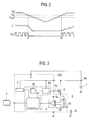
- FIGS. 1 and 2 are flowchart and waveform diagram illustrating operation of the switching apparatus according to the related art.
- VB' is a power source voltage supplied to the control circuit
- Vth' is the predetermined value to stop the control circuit
- Vamin' is a minimum operation voltage of the control circuit
- IL' is a load current passing through the solenoid
- VG' is a gate drive signal to control ON/OFF of the switching element.
- step S101 the switching apparatus carries out a normal operation.
- the control circuit supplies power to the solenoid by controlling the switching element in the PWM manner with the gate drive signal VG' that is a pulse signal alternating H (high) level and L (low) level.
- the gate drive signal VG' is at H-level, the switching element establishes an ON state.
- the load current IL' increases and decreases.
- step S102 the control circuit checks to see if the power source voltage VB' is lower than the predetermined value Vth'. If the power source voltage VB' is equal to or higher than the predetermined value Vth', the switching apparatus continues the normal operation in step S101. If the power source voltage VB' is lower than the predetermined value Vth', the control circuit stops in step S103.
- an operating state of a peripheral device causes the DC voltage VB' to become lower than the predetermined value Vth' and the control circuit stops the switching element by setting the gate drive signal VG' at L-level.
- step S104 the control circuit checks to see if the power source voltage VB' is equal to or higher than the predetermined value Vth'. If the power source voltage VB' is equal to or higher than the predetermined value Vth', the control circuit restarts the switching element in step S105. If the power source voltage VB' is lower than the predetermined value Vth', the control circuit continuously makes the switching element inoperative in step S103.
- the control circuit keeps stopping the switching element by maintaining the gate drive signal VG' at L-level. Thereafter, at time t2', the DC voltage VB' becomes higher than the predetermined value Vth' and the control circuit restarts the PWM control of the switching element by outputting the gate drive signal VG'.
- the load current IL' starts to increase and decrease.
- step S106 the switching apparatus carries out the normal operation, like in step S101.
- the switching apparatus with UVLO function repeats the above-mentioned operation, thereby preventing a malfunction of the control circuit when the DC voltage VB' drops.
- Elements that constitute the control circuit have individual minimum operation voltages (lower limit voltage values for normal operation).
- the predetermined value Vth' for stopping the control circuit is set according to a highest one among the minimum operation voltages of the elements.
- the predetermined value Vth' of the switching apparatus of the related art is set to be higher than the minimum operation voltage value of an amplifier to detect the load current IL.
- the switching apparatus with UVLO function sets the predetermined value Vth' at a relatively high value, to raise a problem to narrow a voltage range in which the solenoid is controlled.
- the present invention provides a switching apparatus with UVLO function, capable of operating in a wider voltage range.
- the switching apparatus includes a DC voltage output unit to output a DC voltage, a switching element to supply the DC voltage to a load, a power detection unit to detect power supplied from the switching element to the load, a drive unit to PWM-control the switching element according to an output from the power detection unit, and a stop unit to stop the PWM control if a value of the DC voltage is smaller than a first threshold value.
- the switching apparatus is characterized in that the first threshold value is smaller than a minimum operation voltage value of the power detection unit.
- a control method of a switching apparatus that PWM-controls a switching element and supplies a DC voltage to a load.
- the method is characterized in that the method PWM-controls the switching element according to an output from a power detection unit that detects power supplied from the switching element to the load, and if a value of the DC voltage is smaller than a minimum operation voltage value of the power detection unit, stops the PWM control.
- the switching apparatus 1 includes a battery 1 serving as a DC voltage output unit to supply power to a control circuit and other load, a switching element 2 to open and close a path between the battery 1 and a solenoid (load) 6, a current detection unit (power detection unit) 3 to detect a current passing through the solenoid 6, a drive unit 4 to control the switching element 2 in the PWM manner according to an output from the current detection unit 3 and a control target value from a microcontroller 7, and a stop unit 5 to detect a decrease in a DC voltage VB and stop the PWM control by the drive unit 4.
- the current detection unit 3, drive unit 4, and stop unit 5 constitute the control circuit 100.
- the battery 1 is a rechargeable battery to output the DC voltage VB to a drain terminal of the switching element 2 and the control circuit 100. Instead of the battery 1, a circuit to rectify a commercial power source and output a DC voltage is adoptable.
- the switching element 2 is a MOSFET with the drain terminal thereof connected to the battery 1.
- a gate drive signal VG that is a pulse signal supplied from the control circuit 100 to a gate terminal of the MOSFET
- the MOSFET intermittently outputs the DC voltage VB from a source terminal thereof to the current detection unit 3 and to the solenoid 6.
- the switching element 2 may be a bipolar transistor, an IGBT (insulated gate bipolar transistor), or the like.
- the current detection unit 3 has a current detection resistor 31 and a current detection amplifier 32.
- a first end of the current detection resistor 31 is connected to the source terminal of the switching element 2 and a second end thereof is connected to a first end of the solenoid 6 serving as a load.
- the current detection resistor 31 detects a load current IL passing through the solenoid 6 and outputs voltage signals to input terminals of the current detection amplifier 32.
- the current detection amplifier 32 is driven with the DC voltage VB, to amplify voltage signals inputted through the inverting and noninverting input terminals thereof and output a detection signal to the drive unit 4.
- the current detection amplifier 32 has a minimum operation voltage Vamin, and when the DC voltage VB exceeds Vamin, normally detects the load current IL.
- the drive unit 4 has an operation circuit 41, an AND gate 42, and a driver circuit 43.
- the operation circuit 41 synchronizes with a clock signal supplied from the microcontroller 7, calculates a duty ratio (ON width) of the gate drive signal, i.e., a pulse signal according to the detection signal supplied from the current detection unit 3 and the control target value supplied from the microcontroller 7, and outputs a PWM signal based on a result of the calculation to a first input terminal of the AND gate 42.
- a second input terminal of the AND gate 42 is connected to the stop unit 5 and an output terminal thereof is connected to the driver circuit 43.
- the driver circuit 43 receives a voltage stepped up from the DC voltage VB from a charge pump circuit (not illustrated) and outputs an output from the AND circuit 42 as the gate driver signal VG to the gate terminal of the switching element 2.
- the operation circuit 41 has a threshold value Vth2 (second threshold value) higher than the minimum operation voltage Vamin of the current detection amplifier 32 and includes a sample-and-hold unit (not illustrated) operating according to a result of comparison between the DC voltage VB and the threshold value Vth2. If the DC voltage VB is higher than the threshold value Vth2, the sample-and-hold unit synchronizes with the clock signal supplied from the microcontroller 7 to periodically reset and hold duty information (calculation result) and output the PWM signal based on the held duty information to the AND gate 42. If the DC voltage VB is lower than the threshold value Vth2, the sample-and-hold unit holds duty information sampled just before the DC voltage VB becomes lower than the threshold value Vth2 and suspends the repetition of reset and hold. Namely, if a relationship of Vth2 > VB is satisfied, the operation circuit 41 outputs a PWM signal of a constant duty ratio to the AND gate 42.
- Vth2 second threshold value
- the stop unit 5 has a threshold value Vth1 (first threshold value), divides the DC voltage VB supplied from the battery 1, compares the divided voltage with the threshold value Vth1, and outputs a result of the comparison as a stop signal to the second input terminal of the AND gate 42.
- the stop unit 5 illustrated in Fig. 3 outputs a stop signal of H (high) level if the DC voltage VB is above the threshold value Vth1 and a stop signal of L (low) level if the DC voltage VB is below the threshold value Vth1.
- the threshold value Vth1 is set to be lower than the minimum operation voltage Vamin of the current detection amplifier 32 and higher than minimum operation voltages of elements, except the current detection amplifier 32, that constitute the control circuit 100.
- the solenoid 6 has the first end connected to the second end of the current detection resistor 31 and a second end connected to the ground.
- the solenoid 6 is an actuator to provide a predetermined displacement according to the magnitude of the load current IL.
- a regenerative diode (not illustrated) is connected in parallel with the solenoid 6, a regenerative diode (not illustrated) is connected.
- the microcontroller 7 outputs the control target value and control clock signal to the drive unit 4.
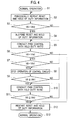
- Figures 4 and 5 are flowchart and waveform diagram illustrating operation of the switching apparatus according to the present invention illustrated in Fig. 3 .
- step S1 the switching apparatus carries out a normal operation.
- the drive unit 4 in the normal operation supplies power to the solenoid 6 by starting the PWM control of the switching element 2 by outputting the gate drive signal VG, i.e., a pulse signal alternating at H (high) level and L (low) level.
- the load current IL increases and decreases.
- step S2 the operation circuit 41 brings a detection signal from the current detection unit 3 closer to a control target value from the microcontroller 7 by calculating a duty ratio (ON width), conducting the sample-and-hold function of periodically repeating the reset and hold of duty information, and outputting a PWM signal based on the held duty information to the AND gate 42.
- a duty ratio ON width
- step S3 the control circuit 100 checks to see if the power source voltage VB is lower than the threshold value Vth2. If the power source voltage VB is equal to or higher than the threshold value Vth2, step S2 is carried out so that the switching apparatus conducts the normal operation and the operation circuit 41 periodically repeats the reset and hold of duty information with the sample-and-hold unit. If the power source voltage VB is lower than the threshold value Vth2, step S4 is carried out so that the operation circuit 41 suspends the reset and hold of duty information by the sample-and-hold unit. In step S5, the control circuit 100 uses a duty ratio held just before the DC voltage VB becomes lower than the threshold value Vth2, to control the switching element 2 in the PWM manner.
- the operating condition of a peripheral device causes the DC voltage VB to decrease lower than the threshold value Vth2 and the operation circuit 41 suspends the repetition of reset and hold of duty information. Accordingly, the duty ratio of the gate drive signal VG is equalized to the duty ratio held just before time t1 when the DC voltage VB decreases lower than the threshold value Vth2.
- step S6 the control circuit 100 checks to see if the power source voltage VB is lower than the threshold value Vth2. If the power source voltage VB is equal to or higher than the threshold value Vth2, step S12 is carried out so that the operation circuit 41 conducts the sample-and-hold function to restart the reset and hold of duty information, and in step S13, the switching apparatus carries out the normal operation. If the power source voltage VB is lower than the threshold value Vth2, the control circuit 100 continuously controls the switching element 2 in a manner of the PWM at the duty ratio held just before the DC voltage VB becomes lower than the threshold value Vth2, and in step S7, the stop unit 5 checks to see if the power source voltage VB is lower than the threshold value Vth1.
- step S7 the power source voltage VB is equal to or higher than the threshold value Vth1
- the control circuit 100 continuously controls, in step S5, the switching element 2 in the PWM manner at the duty ratio held just before the DC voltage VB becomes lower than the threshold value Vth2.
- the control circuit 100 uses, in step S8, the stop unit 5 to stop the PWM control of the switching element 2.
- the DC voltage VB further decreases, and at time t2 illustrated in Fig. 5 , becomes lower than the minimum operation voltage Vamin of the current detection amplifier 32. Then, the current detection amplifier 32 is unable to normally detect the load current IL. At this time, the DC voltage VB is higher than the threshold value Vth1, and therefore, the control circuit 100 continuously controls the switching element 2 in the PWM manner at the constant duty ratio.
- the control circuit 100 depends not on an output from the current detection amplifier 32 but on the duty information held by the sample-and-hold function just before time t1, to generate the gate drive signal VG to control the switching element 2 in a manner of the PWM.
- the DC voltage VB further decreases from time t2, and at time t3 illustrated in Fig. 5 , decreases below the threshold value Vth1. Then, the stop unit 5 outputs a stop signal of L (low) level. During the period from time t3 to time t4, an output from the AND gate 42 becomes L-level without regard to an output from the operation circuit 41, and therefore, the drive signal VG outputted from the driver circuit 43 becomes L-level. Consequently, the control circuit 100 stops the PWM control of the switching element 2.
- step S9 the control circuit 100 checks to see if the power source voltage VB is equal to or higher than the threshold value Vth1. If the power source voltage VB is equal to or higher than the threshold value Vth1, the output from the stop unit 5 becomes H (high) level.
- step S10 the control circuit 100 performs the PWM control of the switching element 2 in a similar manner to step S5 at the duty ratio held just before the DC voltage VB becomes lower than the threshold value Vth2. On the other hand, if the power source voltage VB is lower than the threshold value Vth1, the control circuit 100 makes the switching element 2 inoperative and maintains it in step S8.
- the control circuit 100 makes the stop unit 5 maintain the operation stoppage of the switching element 2 by keeping the gate drive signal VG at L-level.
- the DC voltage VB increases to exceed the threshold value Vth1.
- the stop unit 5 outputs a stop signal of H (high) level.
- the drive unit 4 outputs the gate drive signal VG based on a PWM signal from the operation circuit 41, to restart the PWM control of the switching element 2.
- the operation circuit 41 is suspending the repetition of reset and hold of duty information, and therefore, the outputted PWM signal is based on the duty information held by the sample-and-hold function just before time t1.
- step S11 the control circuit 100 checks to see if the power source voltage VB is equal to or higher than the threshold value Vth2. If the power source voltage VB is equal to or higher than the threshold value Vth2, the operation circuit 41 restarts, in step S12, the repetition of reset and hold of duty information by the sample-and-hold function. On the other hand, if the power source voltage VB is lower than the threshold value Vth2, the control circuit 100 continuously controls the switching element 2 in the PWM manner in step S10 at the duty ratio held just before the DC voltage VB becomes lower than the threshold value Vth2.
- the drive unit 4 performs the PWM control of the switching element 2 in a similar manner to that before time t1 according to a detection signal from the current detection unit 3 and a control target value from the microcontroller 7.
- step S13 the switching apparatus carries out the normal operation similar to step S1.
- the switching apparatus according to this embodiment of the present invention repeats such operation to continuously control the switching element 2 in the PWM manner and drive the solenoid 6 even during the period in which the DC voltage VB becomes lower than the minimum operation voltage Vamin of the current detection amplifier 32 to destabilize the operation of the current detection unit 3.
- the switching apparatus according to this embodiment has below-mentioned effects.
- the present invention is not limited to such a specific embodiment, and within the scope of the present invention mentioned in the claims, allows various modifications and alterations.
- the present invention is applicable to switching apparatuses working for not only solenoids but also motors, LEDs, and lamps and to switching apparatuses for detecting and controlling load voltages.
- the driver circuit 43 may be stopped with a stop signal from the stop unit 5, or a path between the switching element 2 and the driver circuit 43 may be opened according to the stop signal.
- the present invention provides the switching apparatus with UVLO function capable of operating in a wider voltage range.
Landscapes
- Engineering & Computer Science (AREA)
- Power Engineering (AREA)
- Dc-Dc Converters (AREA)
- Electronic Switches (AREA)
Abstract
Description
- The present invention relates to a switching apparatus, and particularly, to a switching apparatus provided with an UVLO (Undervoltage Lockout) function and a controlling method of the same.
- Japanese Unexamined Patent Application Publication No.
2000-114039 - Japanese Unexamined Patent Application Publication No.
2004-22947 - With reference to
Figs. 1 and2 , operation of the UVLO function in the switching apparatus according to the related art will be explained.Figures 1 and2 are flowchart and waveform diagram illustrating operation of the switching apparatus according to the related art. VB' is a power source voltage supplied to the control circuit, Vth' is the predetermined value to stop the control circuit, Vamin' is a minimum operation voltage of the control circuit, IL' is a load current passing through the solenoid, and VG' is a gate drive signal to control ON/OFF of the switching element. - In step S101, the switching apparatus carries out a normal operation. When the DC voltage VB' rises, the control circuit supplies power to the solenoid by controlling the switching element in the PWM manner with the gate drive signal VG' that is a pulse signal alternating H (high) level and L (low) level. When the gate drive signal VG' is at H-level, the switching element establishes an ON state. In response to the operation of the switching element, the load current IL' increases and decreases.
- In step S102, the control circuit checks to see if the power source voltage VB' is lower than the predetermined value Vth'. If the power source voltage VB' is equal to or higher than the predetermined value Vth', the switching apparatus continues the normal operation in step S101. If the power source voltage VB' is lower than the predetermined value Vth', the control circuit stops in step S103.
- Namely, at time t1' illustrated in
Fig. 2 , an operating state of a peripheral device (not illustrated) causes the DC voltage VB' to become lower than the predetermined value Vth' and the control circuit stops the switching element by setting the gate drive signal VG' at L-level. - In step S104, the control circuit checks to see if the power source voltage VB' is equal to or higher than the predetermined value Vth'. If the power source voltage VB' is equal to or higher than the predetermined value Vth', the control circuit restarts the switching element in step S105. If the power source voltage VB' is lower than the predetermined value Vth', the control circuit continuously makes the switching element inoperative in step S103.
- Namely, in the period from time t1' to time t2' illustrated in
Fig. 2 in which the DC voltage VB' is lower than the predetermined value Vth', the control circuit keeps stopping the switching element by maintaining the gate drive signal VG' at L-level. Thereafter, at time t2', the DC voltage VB' becomes higher than the predetermined value Vth' and the control circuit restarts the PWM control of the switching element by outputting the gate drive signal VG'. When the switching element restarts, the load current IL' starts to increase and decrease. - In step S106, the switching apparatus carries out the normal operation, like in step S101.
- The switching apparatus with UVLO function according to the related art repeats the above-mentioned operation, thereby preventing a malfunction of the control circuit when the DC voltage VB' drops.
- Elements that constitute the control circuit have individual minimum operation voltages (lower limit voltage values for normal operation). The predetermined value Vth' for stopping the control circuit is set according to a highest one among the minimum operation voltages of the elements. For example, the predetermined value Vth' of the switching apparatus of the related art is set to be higher than the minimum operation voltage value of an amplifier to detect the load current IL.
- Namely, the switching apparatus with UVLO function according to the related art sets the predetermined value Vth' at a relatively high value, to raise a problem to narrow a voltage range in which the solenoid is controlled.
- With regard to the above-mentioned problem, the present invention provides a switching apparatus with UVLO function, capable of operating in a wider voltage range.
- According to a technical aspect of the present invention, the switching apparatus includes a DC voltage output unit to output a DC voltage, a switching element to supply the DC voltage to a load, a power detection unit to detect power supplied from the switching element to the load, a drive unit to PWM-control the switching element according to an output from the power detection unit, and a stop unit to stop the PWM control if a value of the DC voltage is smaller than a first threshold value. The switching apparatus is characterized in that the first threshold value is smaller than a minimum operation voltage value of the power detection unit.
- According to another technical aspect of the present invention, there is provided a control method of a switching apparatus that PWM-controls a switching element and supplies a DC voltage to a load. The method is characterized in that the method PWM-controls the switching element according to an output from a power detection unit that detects power supplied from the switching element to the load, and if a value of the DC voltage is smaller than a minimum operation voltage value of the power detection unit, stops the PWM control.
-
-
Fig. 1 is a flowchart illustrating operation of a switching apparatus according to a related art. -
Fig. 2 is a waveform diagram illustrating operation of each part of the switching apparatus according to the related art. -
Fig. 3 is a circuit diagram illustrating a configuration of a switching apparatus according to an embodiment of the present invention. -
Fig. 4 is a flowchart illustrating operation of the switching apparatus according to the embodiment of the present invention. -
Fig. 5 is a waveform diagram illustrating operation of each part of the switching apparatus according to the embodiment of the present invention. - With reference to the drawings, an embodiment of the present invention will be explained. Through the drawings, the same or like parts are represented with the same or like reference marks. The drawings illustrate typical models.
- With reference to
Fig. 3 , a configuration of a switching apparatus according to an embodiment of the present invention will be explained. Theswitching apparatus 1 according to the embodiment illustrated inFig. 3 includes abattery 1 serving as a DC voltage output unit to supply power to a control circuit and other load, aswitching element 2 to open and close a path between thebattery 1 and a solenoid (load) 6, a current detection unit (power detection unit) 3 to detect a current passing through thesolenoid 6, adrive unit 4 to control theswitching element 2 in the PWM manner according to an output from the current detection unit 3 and a control target value from amicrocontroller 7, and astop unit 5 to detect a decrease in a DC voltage VB and stop the PWM control by thedrive unit 4. The current detection unit 3,drive unit 4, andstop unit 5 constitute thecontrol circuit 100. - The
battery 1 is a rechargeable battery to output the DC voltage VB to a drain terminal of theswitching element 2 and thecontrol circuit 100. Instead of thebattery 1, a circuit to rectify a commercial power source and output a DC voltage is adoptable. - The
switching element 2 is a MOSFET with the drain terminal thereof connected to thebattery 1. In response to a gate drive signal VG that is a pulse signal supplied from thecontrol circuit 100 to a gate terminal of the MOSFET, the MOSFET intermittently outputs the DC voltage VB from a source terminal thereof to the current detection unit 3 and to thesolenoid 6. Theswitching element 2 may be a bipolar transistor, an IGBT (insulated gate bipolar transistor), or the like. - The current detection unit 3 has a
current detection resistor 31 and acurrent detection amplifier 32. A first end of thecurrent detection resistor 31 is connected to the source terminal of theswitching element 2 and a second end thereof is connected to a first end of thesolenoid 6 serving as a load. Thecurrent detection resistor 31 detects a load current IL passing through thesolenoid 6 and outputs voltage signals to input terminals of thecurrent detection amplifier 32. Thecurrent detection amplifier 32 is driven with the DC voltage VB, to amplify voltage signals inputted through the inverting and noninverting input terminals thereof and output a detection signal to thedrive unit 4. Thecurrent detection amplifier 32 has a minimum operation voltage Vamin, and when the DC voltage VB exceeds Vamin, normally detects the load current IL. - The
drive unit 4 has anoperation circuit 41, anAND gate 42, and adriver circuit 43. Theoperation circuit 41 synchronizes with a clock signal supplied from themicrocontroller 7, calculates a duty ratio (ON width) of the gate drive signal, i.e., a pulse signal according to the detection signal supplied from the current detection unit 3 and the control target value supplied from themicrocontroller 7, and outputs a PWM signal based on a result of the calculation to a first input terminal of theAND gate 42. A second input terminal of theAND gate 42 is connected to thestop unit 5 and an output terminal thereof is connected to thedriver circuit 43. Thedriver circuit 43 receives a voltage stepped up from the DC voltage VB from a charge pump circuit (not illustrated) and outputs an output from theAND circuit 42 as the gate driver signal VG to the gate terminal of theswitching element 2. - The
operation circuit 41 has a threshold value Vth2 (second threshold value) higher than the minimum operation voltage Vamin of thecurrent detection amplifier 32 and includes a sample-and-hold unit (not illustrated) operating according to a result of comparison between the DC voltage VB and the threshold value Vth2. If the DC voltage VB is higher than the threshold value Vth2, the sample-and-hold unit synchronizes with the clock signal supplied from themicrocontroller 7 to periodically reset and hold duty information (calculation result) and output the PWM signal based on the held duty information to theAND gate 42. If the DC voltage VB is lower than the threshold value Vth2, the sample-and-hold unit holds duty information sampled just before the DC voltage VB becomes lower than the threshold value Vth2 and suspends the repetition of reset and hold. Namely, if a relationship of Vth2 > VB is satisfied, theoperation circuit 41 outputs a PWM signal of a constant duty ratio to the ANDgate 42. - The
stop unit 5 has a threshold value Vth1 (first threshold value), divides the DC voltage VB supplied from thebattery 1, compares the divided voltage with the threshold value Vth1, and outputs a result of the comparison as a stop signal to the second input terminal of the ANDgate 42. Thestop unit 5 illustrated inFig. 3 outputs a stop signal of H (high) level if the DC voltage VB is above the threshold value Vth1 and a stop signal of L (low) level if the DC voltage VB is below the threshold value Vth1. The threshold value Vth1 is set to be lower than the minimum operation voltage Vamin of thecurrent detection amplifier 32 and higher than minimum operation voltages of elements, except thecurrent detection amplifier 32, that constitute thecontrol circuit 100. - The
solenoid 6 has the first end connected to the second end of thecurrent detection resistor 31 and a second end connected to the ground. Thesolenoid 6 is an actuator to provide a predetermined displacement according to the magnitude of the load current IL. In parallel with thesolenoid 6, a regenerative diode (not illustrated) is connected. - The
microcontroller 7 outputs the control target value and control clock signal to thedrive unit 4. - With reference to
Figs. 4 and5 , operation of the switching apparatus according to the embodiment will be explained. -
Figures 4 and5 are flowchart and waveform diagram illustrating operation of the switching apparatus according to the present invention illustrated inFig. 3 . - In step S1, the switching apparatus carries out a normal operation. When the DC voltage VB rises, the
drive unit 4 in the normal operation supplies power to thesolenoid 6 by starting the PWM control of theswitching element 2 by outputting the gate drive signal VG, i.e., a pulse signal alternating at H (high) level and L (low) level. In response to the operation of the switching element, the load current IL increases and decreases. - In step S2, the
operation circuit 41 brings a detection signal from the current detection unit 3 closer to a control target value from themicrocontroller 7 by calculating a duty ratio (ON width), conducting the sample-and-hold function of periodically repeating the reset and hold of duty information, and outputting a PWM signal based on the held duty information to the ANDgate 42. - In step S3, the
control circuit 100 checks to see if the power source voltage VB is lower than the threshold value Vth2. If the power source voltage VB is equal to or higher than the threshold value Vth2, step S2 is carried out so that the switching apparatus conducts the normal operation and theoperation circuit 41 periodically repeats the reset and hold of duty information with the sample-and-hold unit. If the power source voltage VB is lower than the threshold value Vth2, step S4 is carried out so that theoperation circuit 41 suspends the reset and hold of duty information by the sample-and-hold unit. In step S5, thecontrol circuit 100 uses a duty ratio held just before the DC voltage VB becomes lower than the threshold value Vth2, to control the switchingelement 2 in the PWM manner. - Namely, at time t1 illustrated in
Fig. 5 , the operating condition of a peripheral device (not illustrated) causes the DC voltage VB to decrease lower than the threshold value Vth2 and theoperation circuit 41 suspends the repetition of reset and hold of duty information. Accordingly, the duty ratio of the gate drive signal VG is equalized to the duty ratio held just before time t1 when the DC voltage VB decreases lower than the threshold value Vth2. - In step S6, the
control circuit 100 checks to see if the power source voltage VB is lower than the threshold value Vth2. If the power source voltage VB is equal to or higher than the threshold value Vth2, step S12 is carried out so that theoperation circuit 41 conducts the sample-and-hold function to restart the reset and hold of duty information, and in step S13, the switching apparatus carries out the normal operation. If the power source voltage VB is lower than the threshold value Vth2, thecontrol circuit 100 continuously controls the switchingelement 2 in a manner of the PWM at the duty ratio held just before the DC voltage VB becomes lower than the threshold value Vth2, and in step S7, thestop unit 5 checks to see if the power source voltage VB is lower than the threshold value Vth1. - In a case where, in step S7, the power source voltage VB is equal to or higher than the threshold value Vth1, the
control circuit 100 continuously controls, in step S5, the switchingelement 2 in the PWM manner at the duty ratio held just before the DC voltage VB becomes lower than the threshold value Vth2. On the other hand, if the power source voltage VB is lower than the threshold value Vth1, thecontrol circuit 100 uses, in step S8, thestop unit 5 to stop the PWM control of theswitching element 2. - From time t1, the DC voltage VB further decreases, and at time t2 illustrated in
Fig. 5 , becomes lower than the minimum operation voltage Vamin of thecurrent detection amplifier 32. Then, thecurrent detection amplifier 32 is unable to normally detect the load current IL. At this time, the DC voltage VB is higher than the threshold value Vth1, and therefore, thecontrol circuit 100 continuously controls the switchingelement 2 in the PWM manner at the constant duty ratio. - Namely, in the period from time t1 to time t3 illustrated in
Fig. 5 , thecontrol circuit 100 depends not on an output from thecurrent detection amplifier 32 but on the duty information held by the sample-and-hold function just before time t1, to generate the gate drive signal VG to control the switchingelement 2 in a manner of the PWM. - The DC voltage VB further decreases from time t2, and at time t3 illustrated in
Fig. 5 , decreases below the threshold value Vth1. Then, thestop unit 5 outputs a stop signal of L (low) level. During the period from time t3 to time t4, an output from the ANDgate 42 becomes L-level without regard to an output from theoperation circuit 41, and therefore, the drive signal VG outputted from thedriver circuit 43 becomes L-level. Consequently, thecontrol circuit 100 stops the PWM control of theswitching element 2. - In step S9, the
control circuit 100 checks to see if the power source voltage VB is equal to or higher than the threshold value Vth1. If the power source voltage VB is equal to or higher than the threshold value Vth1, the output from thestop unit 5 becomes H (high) level. In step S10, thecontrol circuit 100 performs the PWM control of theswitching element 2 in a similar manner to step S5 at the duty ratio held just before the DC voltage VB becomes lower than the threshold value Vth2. On the other hand, if the power source voltage VB is lower than the threshold value Vth1, thecontrol circuit 100 makes the switchingelement 2 inoperative and maintains it in step S8. - Namely, in the period from time t3 to time t4 illustrated in
Fig. 5 , i.e., in the period in which the DC voltage VB is lower than the threshold value Vth1, thecontrol circuit 100 makes thestop unit 5 maintain the operation stoppage of theswitching element 2 by keeping the gate drive signal VG at L-level. - At time t4 illustrated in
Fig. 5 , the DC voltage VB increases to exceed the threshold value Vth1. Then, thestop unit 5 outputs a stop signal of H (high) level. As a result, thedrive unit 4 outputs the gate drive signal VG based on a PWM signal from theoperation circuit 41, to restart the PWM control of theswitching element 2. At this time, theoperation circuit 41 is suspending the repetition of reset and hold of duty information, and therefore, the outputted PWM signal is based on the duty information held by the sample-and-hold function just before time t1. - In step S11, the
control circuit 100 checks to see if the power source voltage VB is equal to or higher than the threshold value Vth2. If the power source voltage VB is equal to or higher than the threshold value Vth2, theoperation circuit 41 restarts, in step S12, the repetition of reset and hold of duty information by the sample-and-hold function. On the other hand, if the power source voltage VB is lower than the threshold value Vth2, thecontrol circuit 100 continuously controls the switchingelement 2 in the PWM manner in step S10 at the duty ratio held just before the DC voltage VB becomes lower than the threshold value Vth2. - Namely, at time t5 illustrated in
Fig. 5 , the DC voltage VB increases higher than that of time t4 and exceeds the threshold value Vth2. Then, theoperation circuit 41 restarts, as the normal operation, the repetition of reset and hold of duty information by the sample-and-hold function. As a result, thedrive unit 4 performs the PWM control of theswitching element 2 in a similar manner to that before time t1 according to a detection signal from the current detection unit 3 and a control target value from themicrocontroller 7. - In step S13, the switching apparatus carries out the normal operation similar to step S1. The switching apparatus according to this embodiment of the present invention repeats such operation to continuously control the switching
element 2 in the PWM manner and drive thesolenoid 6 even during the period in which the DC voltage VB becomes lower than the minimum operation voltage Vamin of thecurrent detection amplifier 32 to destabilize the operation of the current detection unit 3. - The switching apparatus according to this embodiment has below-mentioned effects.
- (i) The threshold value Vth1 for the inoperative state of the
switching element 2 is set to be lower than the minimum operation voltage Vamin of thecurrent detection amplifier 32. This widens a voltage range in which the switching apparatus with UVLO (Undervoltage Lockout) function can operate to a lower voltage side. - (ii) When the DC voltage VB is equal to or lower than the threshold value Vth2, the
drive unit 4 drives the switchingelement 2 in the PWM manner at a duty ratio (ON width) equal to that held just before the DC voltage VB becomes lower than the threshold value Vth2. The threshold value Vth2 is set to be higher than the minimum operation voltage Vamin of thecurrent detection amplifier 32, and therefore, a sharp increase or decrease in the load current IL due to an erroneous operation or the like of thecurrent detection amplifier 32 hardly occurs, and therefore, thesolenoid 6 is properly driven. - (iii) When the
control circuit 100 restarts, the switchingelement 2 is controlled in the PWM manner at the held duty ratio. Compared with restarting the PWM control at a minimum duty ratio, the load current IL quickly rises. - (iv) When the
control circuit 100 restarts, the switchingelement 2 is controlled in the PWM manner at the held duty ratio. Compared with restarting the PWM control at a maximum duty ratio, thesolenoid 6 is prevented from being broken with an overcurrent. - Although the present invention has exemplary been explained according to an embodiment of the present invention, the present invention is not limited to such a specific embodiment, and within the scope of the present invention mentioned in the claims, allows various modifications and alterations. For example, the present invention is applicable to switching apparatuses working for not only solenoids but also motors, LEDs, and lamps and to switching apparatuses for detecting and controlling load voltages. As a means to perform the PWM control of the
switching element 2 at a given duty ratio (ON width), it is possible to continue the repetition of reset and hold of duty information and hold a control target value from themicrocontroller 7 and a detection signal from the current detection unit 3. As a means to make the PWM control inoperative by way of thecontrol circuit 100, thedriver circuit 43 may be stopped with a stop signal from thestop unit 5, or a path between the switchingelement 2 and thedriver circuit 43 may be opened according to the stop signal. - As mentioned above, the present invention provides the switching apparatus with UVLO function capable of operating in a wider voltage range.
- In connection with United States designation, this international patent application claims the benefit of priority under 35 U.S.C. 119(a) to Japanese Patent Application No.
2009-106464 filed on April 24, 2009
Claims (7)
- A switching apparatus comprising:a DC voltage output unit to output a DC voltage;a switching element supplying the DC voltage to a load;a power detection unit detecting power supplied from the switching element to the load;a driver configured to control the switching element in a manner of PWM according to an output from the power detection unit; anda stop unit configured to stop the PWM control if a value of the DC voltage is lower than a first threshold value, whereinthe first threshold value is lower than a minimum operation voltage value of the power detection unit.
- The switching apparatus as set forth in claim 1, wherein
the apparatus has a second threshold value higher than the minimum operation voltage value of the power detection unit, and
if the value of the DC voltage is lower than the second threshold value, the driver controls the switching element at a constant duty ratio. - The switching apparatus as set forth in claim 2, wherein
the driver periodically holds and resets a duty ratio for controlling the switching element in the PWM manner, and
if the value of the DC voltage is lower than the second threshold value, the driver controls the switching element at a duty ratio held in the drive unit. - The switching apparatus as set forth in claim 1 or 2, wherein the load is a solenoid that provides a predetermined displacement according to a supplied current.
- The switching apparatus as set forth in claim 4, wherein the power detection unit detects the current supplied to the load.
- The switching apparatus as set forth in claim 1 or 2, wherein the DC voltage output unit is a battery.
- A control method of a switching apparatus for controlling a switching element in a manner of PWM for supplying a DC voltage to a load, comprising:controlling the switching element in the PWM manner according to an output from a power detector that detects power supplied from the switching element to the load; andstopping the PWM control of the switching element when a value of the DC voltage is lower than a first threshold value that is lower than a minimum operation voltage value of the power detector.
Applications Claiming Priority (2)
| Application Number | Priority Date | Filing Date | Title |
|---|---|---|---|
| JP2009106464A JP5229495B2 (en) | 2009-04-24 | 2009-04-24 | Switching device and control method thereof |
| PCT/JP2010/055112 WO2010122870A1 (en) | 2009-04-24 | 2010-03-24 | Switching device and method for controlling same |
Publications (2)
| Publication Number | Publication Date |
|---|---|
| EP2424091A1 true EP2424091A1 (en) | 2012-02-29 |
| EP2424091A4 EP2424091A4 (en) | 2017-06-14 |
Family
ID=43010993
Family Applications (1)
| Application Number | Title | Priority Date | Filing Date |
|---|---|---|---|
| EP10766929.3A Withdrawn EP2424091A4 (en) | 2009-04-24 | 2010-03-24 | Switching device and method for controlling same |
Country Status (5)
| Country | Link |
|---|---|
| US (1) | US8711529B2 (en) |
| EP (1) | EP2424091A4 (en) |
| JP (1) | JP5229495B2 (en) |
| CN (1) | CN102171916B (en) |
| WO (1) | WO2010122870A1 (en) |
Cited By (2)
| Publication number | Priority date | Publication date | Assignee | Title |
|---|---|---|---|---|
| CN103249221A (en) * | 2012-02-13 | 2013-08-14 | 松下电器产业株式会社 | Power supply device and lighting device and lighting fixture using the same |
| EP2711138A3 (en) * | 2012-09-13 | 2016-11-02 | Panasonic Intellectual Property Management Co., Ltd. | Power tool |
Families Citing this family (8)
| Publication number | Priority date | Publication date | Assignee | Title |
|---|---|---|---|---|
| WO2012127515A1 (en) * | 2011-03-18 | 2012-09-27 | 三菱電機株式会社 | Led lighting device |
| US8786264B2 (en) | 2012-01-11 | 2014-07-22 | Blackberry Limited | DCDC converter with converter modules that can be dynamically enabled or disabled |
| CN102856876B (en) * | 2012-09-25 | 2015-10-21 | 广东易事特电源股份有限公司 | A kind of Anti-misreport island detection system |
| JP6119244B2 (en) * | 2012-12-28 | 2017-04-26 | 大日本印刷株式会社 | Power switch circuit and battery-powered device |
| CN104883059B (en) * | 2015-05-21 | 2018-06-05 | 上海长园维安电子线路保护有限公司 | Dual chip power protector and battery-powered electronic product protection circuit |
| CN110692117B (en) * | 2017-05-31 | 2022-05-17 | 本田技研工业株式会社 | Microcomputer input switch |
| FR3075511A1 (en) * | 2017-12-18 | 2019-06-21 | Stmicroelectronics (Grenoble 2) Sas | CUTTING POWER SUPPLY AND ITS CONTROL METHOD |
| US12519409B2 (en) * | 2023-06-06 | 2026-01-06 | Kinetic Technologies International Holdings Lp | Method of rotor angle estimation for a multi-phase permanent magnet rotor motor |
Family Cites Families (8)
| Publication number | Priority date | Publication date | Assignee | Title |
|---|---|---|---|---|
| JPH02176901A (en) * | 1988-12-28 | 1990-07-10 | Toyota Motor Corp | Electric conduction controller for load |
| KR0162847B1 (en) * | 1996-03-08 | 1999-04-15 | 김광호 | Switched-Mode Power Supplies with Overcurrent and Overvoltage Protection |
| JP2000114039A (en) | 1998-09-29 | 2000-04-21 | Denso Corp | Linear solenoid failure detection device |
| JP2004022947A (en) * | 2002-06-19 | 2004-01-22 | Tamura Seisakusho Co Ltd | Transition regulating apparatus of uvlo |
| US7345894B2 (en) * | 2005-09-27 | 2008-03-18 | Carl Sawtell | Cascode switch power supply |
| JP2008304041A (en) * | 2007-06-11 | 2008-12-18 | Aisin Aw Co Ltd | Faulty moving detecting device |
| JP2009027773A (en) * | 2007-07-17 | 2009-02-05 | Hitachi Ltd | Power supply device, IC circuit, information processing device, and soft start control method |
| JP2009106464A (en) | 2007-10-30 | 2009-05-21 | Yamatani Inc | Odor-absorbing sheet and method of manufacturing the same |
-
2009
- 2009-04-24 JP JP2009106464A patent/JP5229495B2/en active Active
-
2010
- 2010-03-24 CN CN201080002781.8A patent/CN102171916B/en active Active
- 2010-03-24 EP EP10766929.3A patent/EP2424091A4/en not_active Withdrawn
- 2010-03-24 WO PCT/JP2010/055112 patent/WO2010122870A1/en not_active Ceased
- 2010-03-24 US US13/121,958 patent/US8711529B2/en active Active
Non-Patent Citations (1)
| Title |
|---|
| See references of WO2010122870A1 * |
Cited By (2)
| Publication number | Priority date | Publication date | Assignee | Title |
|---|---|---|---|---|
| CN103249221A (en) * | 2012-02-13 | 2013-08-14 | 松下电器产业株式会社 | Power supply device and lighting device and lighting fixture using the same |
| EP2711138A3 (en) * | 2012-09-13 | 2016-11-02 | Panasonic Intellectual Property Management Co., Ltd. | Power tool |
Also Published As
| Publication number | Publication date |
|---|---|
| US20110176249A1 (en) | 2011-07-21 |
| JP2010259222A (en) | 2010-11-11 |
| JP5229495B2 (en) | 2013-07-03 |
| CN102171916B (en) | 2014-03-26 |
| CN102171916A (en) | 2011-08-31 |
| US8711529B2 (en) | 2014-04-29 |
| EP2424091A4 (en) | 2017-06-14 |
| WO2010122870A1 (en) | 2010-10-28 |
Similar Documents
| Publication | Publication Date | Title |
|---|---|---|
| US8711529B2 (en) | Switching apparatus and controlling method thereof | |
| US8625249B2 (en) | Control apparatus for electromagnetic inductive load | |
| US7129679B2 (en) | Power supply circuit having soft start | |
| US7638954B2 (en) | Light emitting diode drive apparatus | |
| US6734639B2 (en) | Sample and hold method to achieve square-wave PWM current source for light emitting diode arrays | |
| JP4060840B2 (en) | Light emitting diode driving semiconductor circuit and light emitting diode driving device having the same | |
| EP2549835B1 (en) | Led short circuit protection | |
| CN104995997B (en) | Electric supply installation | |
| US20110291634A1 (en) | Overcurrent protection circuit and overcurrent protection method | |
| US20090243568A1 (en) | Method and apparatus for synchronous boost voltage regulators with active negative current modulation | |
| US8400078B2 (en) | LED driving circuit and driving controller for controlling the same | |
| EP2362712A2 (en) | Led Lighting Circuit | |
| US11942925B2 (en) | Management of multiple switching-synchronized measurements using combined prioritized measurement and round-robin sequence measurement | |
| US10756626B2 (en) | Power conversion circuit | |
| TW201215224A (en) | Open LED control circuit and associated method | |
| CN101849273B (en) | Apparatus and method for supplying power to a voltage- or current-releasing switching device | |
| US8681514B2 (en) | Controller for secondary side control of a switch, power converter, and related synchronous rectification control method | |
| US20180309435A1 (en) | Control circuit | |
| JP2018157695A (en) | Driving circuit and light-emitting device | |
| US9603227B2 (en) | Semiconductor light source driving apparatus | |
| US7746017B2 (en) | Fan driving system with safe driving current switching | |
| CN102281686B (en) | Compensation control device for LED (Light Emitting Diode) lamp during rapid falling of input voltage and method thereof | |
| KR101196199B1 (en) | Circuit for blocking overcurrent in dc/dc converter | |
| JP2020198243A (en) | Led driving device and display apparatus, and control apparatus for led driving device | |
| JP4174999B2 (en) | DC / DC converter |
Legal Events
| Date | Code | Title | Description |
|---|---|---|---|
| PUAI | Public reference made under article 153(3) epc to a published international application that has entered the european phase |
Free format text: ORIGINAL CODE: 0009012 |
|
| 17P | Request for examination filed |
Effective date: 20110330 |
|
| AK | Designated contracting states |
Kind code of ref document: A1 Designated state(s): AT BE BG CH CY CZ DE DK EE ES FI FR GB GR HR HU IE IS IT LI LT LU LV MC MK MT NL NO PL PT RO SE SI SK SM TR |
|
| DAX | Request for extension of the european patent (deleted) | ||
| RA4 | Supplementary search report drawn up and despatched (corrected) |
Effective date: 20170512 |
|
| RIC1 | Information provided on ipc code assigned before grant |
Ipc: H02M 3/00 20060101AFI20170508BHEP Ipc: H02M 1/32 20070101ALI20170508BHEP Ipc: H02M 1/36 20070101ALI20170508BHEP |
|
| 17Q | First examination report despatched |
Effective date: 20180122 |
|
| STAA | Information on the status of an ep patent application or granted ep patent |
Free format text: STATUS: THE APPLICATION HAS BEEN WITHDRAWN |
|
| 18W | Application withdrawn |
Effective date: 20180410 |