EP2424038A1 - Reflectarray - Google Patents
Reflectarray Download PDFInfo
- Publication number
- EP2424038A1 EP2424038A1 EP11179107A EP11179107A EP2424038A1 EP 2424038 A1 EP2424038 A1 EP 2424038A1 EP 11179107 A EP11179107 A EP 11179107A EP 11179107 A EP11179107 A EP 11179107A EP 2424038 A1 EP2424038 A1 EP 2424038A1
- Authority
- EP
- European Patent Office
- Prior art keywords
- reflectarray
- patches
- fingers
- shape
- gap
- Prior art date
- Legal status (The legal status is an assumption and is not a legal conclusion. Google has not performed a legal analysis and makes no representation as to the accuracy of the status listed.)
- Granted
Links
Images







Classifications
-
- H—ELECTRICITY
- H01—ELECTRIC ELEMENTS
- H01Q—ANTENNAS, i.e. RADIO AERIALS
- H01Q15/00—Devices for reflection, refraction, diffraction or polarisation of waves radiated from an antenna, e.g. quasi-optical devices
- H01Q15/0006—Devices acting selectively as reflecting surface, as diffracting or as refracting device, e.g. frequency filtering or angular spatial filtering devices
- H01Q15/0013—Devices acting selectively as reflecting surface, as diffracting or as refracting device, e.g. frequency filtering or angular spatial filtering devices said selective devices working as frequency-selective reflecting surfaces, e.g. FSS, dichroic plates, surfaces being partly transmissive and reflective
- H01Q15/002—Devices acting selectively as reflecting surface, as diffracting or as refracting device, e.g. frequency filtering or angular spatial filtering devices said selective devices working as frequency-selective reflecting surfaces, e.g. FSS, dichroic plates, surfaces being partly transmissive and reflective said selective devices being reconfigurable or tunable, e.g. using switches or diodes
-
- H—ELECTRICITY
- H01—ELECTRIC ELEMENTS
- H01Q—ANTENNAS, i.e. RADIO AERIALS
- H01Q1/00—Details of, or arrangements associated with, antennas
- H01Q1/36—Structural form of radiating elements, e.g. cone, spiral, umbrella; Particular materials used therewith
- H01Q1/38—Structural form of radiating elements, e.g. cone, spiral, umbrella; Particular materials used therewith formed by a conductive layer on an insulating support
-
- H—ELECTRICITY
- H01—ELECTRIC ELEMENTS
- H01Q—ANTENNAS, i.e. RADIO AERIALS
- H01Q3/00—Arrangements for changing or varying the orientation or the shape of the directional pattern of the waves radiated from an antenna or antenna system
- H01Q3/44—Arrangements for changing or varying the orientation or the shape of the directional pattern of the waves radiated from an antenna or antenna system varying the electric or magnetic characteristics of reflecting, refracting, or diffracting devices associated with the radiating element
- H01Q3/46—Active lenses or reflecting arrays
Definitions
- the present invention relates to a reflectarray.
- the reflector For addressing this problem, it can be considered to incline the reflector such that the reflector looks into the ground. Accordingly, the incident angle and the reflection angle with respect to the reflector can be increased so that an incoming wave can be directed to a desired direction.
- the reflectarray can be designed by arranging phase shifts of reflected waves such that a beam is directed to a desired direction.
- various techniques are introduced such as a method for using a stub, a method for varying sizes and the like (for example, refer to non-patent document 3).
- Non-patent document 1 L. Li et al., "Microstrip reflectarray using crossed-dipole with frequency selective surface of loops," ISAP2008, TP-C05, 1645278 .
- Non-patent document 2 T. Maruyama, T. Furuno, and S. Uebayashi, "Experiment and analysis of reflect beam direction control using a reflector having periodic tapered mushroom-like structure," ISAP2008, MO-IS1, 1644929, p. 9 .
- Non-patent document 3 J. Huang and J. A. Encinar, Reflectarray antennas. Piscataway, N.J.Hoboken: IEEE Press; Wiley-Interscience, 2008 .
- Fig. 2 shows an example of a conventional reflectarray.
- microstrip antennas are used as array elements 10 and a metal flat plate is used as a ground plane 20.
- Fig. 2 shows an example in which the array element 10 is a square. The dimensions a and b of the array element 10 are determined based on a phase shift.
- the present invention is contrived from the viewpoint of the above-mentioned problem, and an object of the present invention is to provide a reflectarray that can widen the phase range of the reflection coefficient, and that can vary the phase shift without varying the size of elements forming the reflectarray.
- An aspect of the present invention provides a reflectarray, including:
- the phase range of the reflection coefficient can be widened. Also, according to the reflectarray, the phase shift can be varied without varying the size of elements forming the reflectarray, so that deterioration of radiation can be prevented.
- Fig. 3 shows a whole structure of the reflectarray
- Fig. 4 shows an array element that forms the reflectarray.
- Fig. 3 shows a reflectarray 100 according to the present embodiment.
- an array element is formed on each of areas obtained by dividing a principal surface on a substrate.
- the array element is formed by a plurality of patches.
- the patches of the array element are placed such that the patches are separated by a predetermined space.
- each area on the substrate on which an array element is formed is called an element cell 200.
- the element cell is also called a periodic cell.
- Each array element has the same size, that is, each of 1 d and W d shown in Fig. 4A is the same in each array element.
- array elements are arranged two-dimensionally in which 7 array elements are arranged in the X direction and 4 array elements are arranged in the Y direction.
- the reflectarray may be configured such that array elements are arranged one-dimensionally.
- the number of the array elements to be arranged is not limited to a particular number. Any number of array elements can be arranged. Details of the reflectarray are described later.
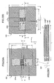
- Figs. 4A and 4B show the element cell 200 according to the present embodiment.
- Fig. 4A shows a top view (viewed from z direction) and
- Fig. 4B shows a section view (showing a section indicated by a dashed line of Fig. 4A viewed from the A direction).
- patches 204a and 204b are formed on a principal surface, by using a conductor, of a substrate 202 of relative permittivity ⁇ r , wherein the element cell 200 forms a square of L on a side.
- a dipole is formed by the patches 204a and 204b.
- a metal reflector 206 is formed on a surface opposite to the surface of the substrate 202 on which the patches 204a and 204b are formed.
- a length of a side of the substrate 202 is indicated as L.
- the L is also a length of a side of the element cell 200.
- the array element may be formed as a rectangle.
- a thickness of the substrate is indicated as t.
- a vertical length of the array element is l d
- a lateral length (width) of the array element is w d
- a predetermined gap 205 is formed between two adjacent patches.
- a fringe capacitor is formed between the adjacent patches by the gap 205.
- the part where the two patches adjoin each other is formed like a comb-shape (207a, 207b) so that the two patches are engaged with each other while being separated by a predetermined gap.
- the comb-shape may be also called a meander.
- a gap of an almost rectangular corrugated shape is formed by arranging the two patches such that the two patches are engaged with each other while they are separated by a predetermined space.
- the shape of the gap is not limited to a particular shape as long as the gap is formed between the two patches.
- the gap may be a line shape, or may be an arbitrary curve such as a sine wave shape, or may be a saw-tooth wave shape.
- a vertical length of the fingers 207a and 207b of the comb-shape is represented by l s
- a lateral length (width) of the finger is represented by w s
- the gap 205 (interval between adjacent fingers of the two patches) is represented by s. Therefore, a pitch of the comb-shape of one patch is represented by 2(w s +s). The pitch indicates a sum of the interval between the adjacent fingers and the width of the finger of the comb-shape.
- w s ⁇ w d -(N-1)s ⁇ /N holds true, in which N indicates the number of the fingers.
- the total number of the fingers is 11 in which the number of the fingers for the patch 204a is 6, and the number for the patch 204b is 5.
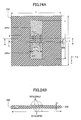
- Figs. 5A and 5B show an example of an array element having a value N different from that of the array element shown in Figs. 4A and 4B .
- the number of the fingers for the patch 204a is 4 and the number of the fingers for the patch 204b is 3, so that the total number is 7.
- Figs. 6, 7A and 7B show examples of dimensions of patches of the element cell 200.
- Fig. 6 shows an example of dimensions of the element cell 200 shown in Figs. 4A and 4B .
- the frequency of the incident wave is 24 GHz.
- L is 5.0[mm]
- l d is 4.0 [mm]
- w d is 1.2 [mm]
- s is 0.05 [mm]
- t is 0.75[mm] and ⁇ r is 2.5.
- Fig. 7A shows an example of dimensions of the element cell 200 shown in Figs. 5A and 5B .
- the frequency of the incident wave is 12 GHz.
- L is 10.0[mm]
- l d is 8.0[mm]
- w d is 2.6[mm]
- s is 0.2[mm]
- t is 1.6[mm] and ⁇ r is 2.5.
- Fig. 7B shows an example of dimensions of the element cell 200 shown in Figs. 5A and 5B .
- the frequency of the incident wave is 3 GHz.
- L is 40.0[mm]
- l d is 32.0 [mm]
- w d is 9. 6 [mm]
- s is 0.4[mm]
- t is 6.0[mm]
- ⁇ r is 2.5.
- Figs. 8-10 shows relationship between the phase (degrees) of the reflection coefficient (which can be also called as Reflection Phase) and the vertical length l s of the fingers (207a, 207b) of the patch.
- the vertical length l s of the fingers (207a, 207b) of the patch is represented as "Length of fingers (l s , mm)”.
- Figs. 8-10 show a case where a planar wave vertically enters a surface of the array element 200.
- Fig. 8 shows a case of 24 GHz
- Fig. 9 shows a case of 3 GHz
- Fig. 10 shows a case of 12 GHz.
- N of fingers (207a, 207b) are 11, 11 and 7 in Figs. 8, 9 and 10 respectively.
- the values of w s are 0.06[mm], 0.5[mm] and 0.2[mm] in Figs. 8, 9 and 10 respectively.
- the values of t are 0.75 mm, 6 mm and 1.6 mm in Figs. 8, 9 and 10 respectively.
- the surface area of each patch that forms the gap between the adjacent patches can be varied.
- the gap corresponds to a loaded load of scattering elements.
- the gap can be also changed by the lateral length (width) of the finger (207a, 207b) of the comb-shape.
- the vertical length l s and/or the lateral length (width) w s of the finger (207a, 207b) of the comb-shape of the patches can be varied in a wide range, a load impedance can be adjusted in a wide range. Since the load impedance can be varied in a wide range, it becomes possible to increase the range within which the phase of the reflection coefficient can be adjusted.
- the part where the two patches face each other is formed as a comb-shape.
- the comb-shape is formed, by varying the length l s of the fingers of the comb-shape, the surface area of each patch that forms the gap between the adjacent patches can be easily varied. Also, processing for fabrication is easy.
- Figs. 8-10 show that a wide phase range of reflection coefficient can be obtained by adjusting the vertical length l s . More particularly, there is a case where equal to or greater than 1000 degrees can be obtained as the phase range of the reflection coefficient.
- the phase of the reflection coefficient may vary according to a frequency to be used and an incident angle.
- Fig. 11 shows relationship between the phase of the reflection coefficient and the vertical length l s of the fingers (207a, 207b) of the comb-shape of the patch for different frequencies of incident wave.
- Fig. 11 shows cases in which the frequencies of the incident wave are 23 GHz, 24 GHz and 25 GHz.
- Fig. 11 in each of the cases of 23 GHz, 24 GHz and 25 GHz, equal to or greater than 1000 degrees can be obtained as the phase range of the reflection coefficient, which indicates that, the reflectarray of the present embodiment can operate in a wide band by designing the reflectarray in consideration of the band.
- Fig. 12 shows relationship between the phase of the reflection coefficient and the vertical length l s of the fingers of the comb-shape of the patch for different incident angles.
- Fig. 12 shows cases in which the incident angles are 30 degrees, 45 degrees and 60 degrees.
- the incident wave is 24 GHz.
- Fig. 12 it can be understood that, since an influence of oblique incidence is not large, the influence can be neglected depending on the size of the reflectarray. However, when the size of the reflectarray becomes large to some extent, it is preferable to consider the influence.
- Fig. 13 shows a design example (1) of a reflectarray.
- array elements are arranged two-dimensionally in which 7 array elements are arranged in the X direction and 4 array elements are arranged in the Y direction.
- the incident wave is 24 GHz.
- the size of the reflectarray is 35[mm] in the X direction and is 20 [mm] in the Y direction.
- the value of t is 0.75 mm. The sizes of each array are almost the same.
- the vertical length l s of the fingers of the comb-shape is different between adjacent array elements.
- Each of the numerical values shown in the left side of Fig. 13 indicates the vertical length l s [mm] of the fingers of the comb-shape of a corresponding array element.
- the vertical length l s of the fingers of the comb-shape is the same between adjacent array elements.
- each vertical length of the fingers of the comb-shape shown in the figure is merely an example, and the length is changeable as necessary.
- the reflectarray may be configured such that the vertical length l s of the fingers is the same between array elements adjacent in the X direction, and that the vertical length l s of the fingers is different between array elements adjacent in the Y direction.
- the length may be different between at least a part of array elements and other array elements.
- the length may be the same in all of the array elements.
- the reflectarray is configured such that the vertical length l s of the fingers is different between adjacent array elements arranged in the X direction, and that the vertical length l s of the fingers is the same between adjacent array elements arranged in the Y direction.
- Fig. 14 shows an example of design dimensions and compensation phase (degree) of the reflectarray 100 shown in Fig. 13 .
- the phase compensated between the array elements that are adjacent in the X direction is about 120 degree.
- Fig. 15 shows an example of a radiation pattern of the reflectarray 100 of the present embodiment.
- the incident wave is 3 GHz
- directivity becomes the maximum.
- the directivity is 14.1 [dBi].
- the direction in which the directivity becomes the maximum is 58 degrees while the design value is 60 degrees, which indicates that difference from the design value of the 58 degrees is small.
- Fig. 16 shows a design example (2) of a reflectarray.
- array elements are arranged two-dimensionally in which 7 array elements are arranged in the X direction and 4 array elements are arranged in the Y direction.
- the incident wave is 3 GHz.
- the size of the reflectarray is 280 [mm] in the X direction and is 160 [mm] in the Y direction.
- the value of t is 6 mm. The sizes of each array element are almost the same.
- the vertical length l s of the fingers of the comb-shape is different between adjacent array elements.
- Each of the numerical values shown in the left side of Fig. 16 indicates the vertical length l s [mm] of the fingers of the comb-shape of a corresponding array element.
- the vertical length l s of the fingers of the comb-shape is the same between adjacent array elements.
- each vertical length of the fingers shown in the figure is merely an example, and the length is changeable as necessary.
- the reflectarray may be configured such that the vertical length l s of the fingers is the same between array elements adjacent in the X direction, and that the vertical length l s of the fingers is different between array elements adjacent in the Y direction.
- the length may be different between at least a part of array elements and other array elements.
- the length may be the same in all of the array elements.
- the reflectarray is configured such that the vertical length l s of the fingers is different between adjacent array elements arranged in the X direction, and that the vertical length l s of the fingers is the same between adjacent array elements arranged in the Y direction.
- Fig. 17 shows an example of design dimensions and compensation phase (degrees) of the reflectarray shown in Fig. 16 .
- the phase compensated between the array elements that are adjacent in the X direction is about 120 degrees.
- Fig. 18 shows a design example (3) of a reflectarray.
- array elements are arranged two-dimensionally in which 11 array elements are arranged in the X direction and 6 array elements are arranged in the Y direction.
- the incident wave is 12 GHz.
- the size of the reflectarray is 110 [mm] in the X direction and is 60 [mm] in the Y direction.
- the value of t is 1.6 mm. The sizes of each array are almost the same.
- the vertical length l s of the fingers of the comb-shape is different between adjacent array elements.
- Each of the numerical values shown in the left side of Fig. 18 indicates the vertical length l s [mm] of the fingers of the comb-shape of a corresponding array element.
- the vertical length l s of the fingers of the comb-shape is the same between adjacent array elements.
- each vertical length of the fingers of the comb-shape shown in the figure is merely an example, and the length is changeable as necessary.
- the reflectarray may be configured such that the vertical length l s of the fingers is the same between array elements adjacent in the X direction, and that the vertical length l s of the fingers is different between array elements adjacent in the Y direction.
- the length may be different between at least a part of array elements and other array elements.
- the length may be the same in all of the array elements.
- the reflectarray is configured such that the vertical length l s of the fingers of the comb-shape is different between adjacent array elements arranged in the X direction, and that the vertical length l s of the fingers of the comb-shape is the same between adjacent array elements arranged in the Y direction.
- Fig. 19 shows an example of design dimensions and compensation phase (degrees) of the reflectarray shown in Fig. 18 .
- the phase compensated between the array elements that are adjacent in the X direction is about 120 degrees.
- Fig. 20 shows an example of a radiation pattern of the reflectarray 100 of the present embodiment.
- the incident wave is 12 GHz, and the directivity gain is 17 [dBi].
- the direction in which the directivity becomes the maximum is 58 degrees while the design value is 60 degrees, which indicates that difference from the design value of the 58 degrees is small.
- a load impedance can be adjusted in a wide range. Since the load impedance can be adjusted in a wide range, it becomes possible to widen the range within which the phase of the reflection coefficient can be adjusted. In the element cell, since it becomes possible to widen the range within which the phase of the reflection coefficient can be adjusted, it also becomes possible to widen the range within which the phase of the reflection coefficient can be adjusted in a reflectarray where a plurality of element cells are arranged.
- a load impedance can be adjusted in a wide range. Since the load impedance can be adjusted in a wide range, it becomes possible to widen the range within which the phase of the reflection coefficient can be adjusted.
- the element cell of the present embodiment by adjusting the gap formed between the adjacent patches, it becomes possible to widen the range within which the phase of the reflection coefficient can be adjusted. Therefore, in a reflectarray where a plurality of element cells are arranged, it becomes possible to widen the range within which the phase of the reflection coefficient can be adjusted without varying the size of each array element. Since it is not necessary to vary the size of the array element, characteristic deterioration of the reflectarray can be decreased, the characteristic deterioration being caused by variations of spaces between adjacent array elements.
- the reflectarray of the present modified example is similar to reflectarrays shown in Figs. 3 and 13 .
- Figs. 21A and 21B show an element cell 200 according to the present modified embodiment.
- Fig. 21A shows a top view (viewed from z direction) and
- Fig. 21B shows a section view (a section indicated by a dashed line in Fig. 21A viewed from the A direction).
- patches 204a, 204b and 204c are formed on a principal surface, by using a conductor, of a substrate 202.
- a metal reflector 206 is formed on a surface opposite to the surface of the substrate 202 on which the patches 204a, 204b and 204c are formed.
- a length of a side of the element cell is indicated as L.
- the substrate 202 is formed by a dielectric.
- a relative permittivity of the substrate 202 is represented by ⁇ r .
- a thickness of the substrate 202 is indicated as t.
- a vertical length of the array element is l d
- a lateral length (width) of the array element is w d
- a predetermined gap is formed between two adjacent patches.
- a fringe capacitor is formed between the adjacent patches by the gap.
- the part where two patches adjoin each other is formed like a comb-shape (207c, 207b, 207e, 207f) so that the two patches are engaged with each other while being separated by a predetermined interval.
- a gap of an almost rectangular corrugated shape is formed.
- the shape of the gap is not limited to the shape shown in the figure as long as the gap is formed between the two patches.
- the gap may be a line shape, or may be an arbitrary curve such as a sine wave shape, or may be a saw-tooth wave shape.
- a vertical length of the fingers 207c and 207d of the comb-shape is represented by l s1
- a lateral length (width) of each finger is represented by W s1
- the gap 205 1 between adjacent fingers of the two patches is represented by s 1 . Therefore, a pitch of the comb-shape of a patch is represented by 2(w s1 +s 1 ). The pitch indicates a sum of the gap between the adjacent fingers and the width of the finger of the comb-shape.
- w sl ⁇ w d -(N-1) s 1 ⁇ /N holds true, in which N indicates the number of fingers.
- the total number of the fingers is 11 in which the number of the fingers for the patch 204a is 6, and the number for the patch 204b adjacent to the patch 204a is 5.
- the value of s 1 indicates an interval between adjacent fingers.
- a vertical length of the fingers 207e and 207f of the comb-shape is represented by l s2
- a lateral length (width) of each finger is represented by w s2
- the gap 205 2 between the adjacent fingers of the two patches is represented by s 2 . Therefore, a pitch of the comb-shape of a patch is represented by 2 (w s2 +s 2 ) . The pitch indicates a sum of the gap between the adjacent fingers and the width of a finger of the comb-shape.
- N 2 indicates the number of fingers.
- the total number of the fingers is 11 in which the number of the fingers for the patch 204b is 6, and the number for the patch 204c adjacent to the patch 204b is 5.
- the value of s 2 indicates an interval between adjacent fingers.
- N and N 2 may be the same or may be different.
- the lengths l s1 and l s2 of the fingers may be the same or may be different. Also, the lateral lengths (widths) w s1 and w s2 of the fingers may be the same or may be different. Also, the gaps S 1 and S 2 between adjacent fingers of two patches may be the same or may be different.
- the number of gaps between patches formed on the element cell 200 is 2
- the number may be equal to or more than 3.
- the shape of each gap may be the same or may be different.
- the reflectarray of the present modified example is similar to reflectarrays shown in Figs. 3 and 13 .
- Figs. 22A and 22B show an element cell 200 according to the present modified embodiment.
- Fig. 22A shows a top view (viewed from z direction) and
- Fig. 22B shows a section view (a section indicated by a dashed line in Fig. 22A viewed from the A direction).
- the shape of the dipole is not limited to a rectangle.
- a shape other than the rectangle a case is described in which the shape of the dipole is configured to be a cross shape.
- patches 204a, 204b and 204c are formed on a principal surface, by using a conductor, of a substrate 202.
- a metal reflector 206 is formed on a surface opposite to the surface of the substrate 202 on which the patches 204a, 204b and 204c are formed.
- a length of a side of the element cell 200 is indicated as L.
- the substrate 202 is formed by a dielectric.
- a relative permittivity of the substrate 202 is represented by ⁇ r .
- a thickness of the substrate 202 is represented by t.
- the dipole has a shape in which parts of two patches overlap, wherein a vertical length of each patch is l d , and a lateral length (width) of each patch is w d .
- a predetermined gap is formed between two adjacent patches.
- a fringe capacitor is formed between the adjacent patches by the gap.
- the part where two patches adjoin each other is formed like a comb-shape (207g, 207h, 207i, 207j) so that the two patches are engaged with each other while being separated by a predetermined space.
- a gap of an almost rectangular corrugated shape is formed by arranging the two patches such that the two patches are engaged with each other while they are separated by a predetermined space.
- the shape of the gap is not limited to the shape shown in the figure as long as the gap is formed between the two patches.
- the gap may be a line shape, or may be an arbitrary curve such as a sine wave shape, or may be a saw-tooth wave shape.
- a vertical length of the fingers 207g and 207h of the comb-shape is represented by l s3
- a lateral length (width) of each finger is represented by w s3
- the gap 205 3 between the adjacent fingers of the two patches is represented by s 3 . Therefore, a pitch of the comb-shape of a patch is represented as 2 (w s3 +s 13 ). The pitch indicates a sum of the interval between the adjacent fingers and the width of a finger of the comb-shape.
- N the number of fingers.
- the total number of the fingers is 11 in which the number of the fingers for the patch 204a is 5, and the number for the patch 204b adjacent to the patch 204a is 6.
- the value of s 3 indicates an interval between adjacent fingers.
- N and N 2 may the same or may be different.
- a vertical length of the fingers 207i and 207j of the comb-shape is represented by l s4
- a lateral length (width) of each finger is represented by w s4
- the gap 205 4 of the adjacent fingers of the two patches is represented by s 4 .
- a pitch of the comb-shape of a patch is represented by 2 (w s4 +s 4 ) .
- the pitch indicates a sum of the interval between the adjacent fingers and the width of a finger of the comb-shape.
- N the number of fingers.
- the total number of the fingers is 11 in which the number of the fingers for the patch 204b is 6, and the number for the patch 204c adjacent to the patch 204b is 5.
- the value of s 4 indicates an interval between adjacent fingers.
- N and N 2 may the same or may be different.
- the lengths l s3 and l s4 of the fingers may be the same or may be different. Also, the lateral lengths (widths) w s3 and w s4 of the fingers may be the same or may be different. Also, the gaps s 3 and s 4 between adjacent fingers may be the same or may be different.
- the number of gaps between patches formed on the element cell 200 is 2
- the number may be equal to or more than 3.
- the shape of each gap may be the same or may be different.
- Figs. 23A-23C show an element cell 200 according to the present modified example.
- a multilayer structure is adopted using three conductive layers and two dielectric layers.
- a multilayer cross dipole reflectarray is configured by crossing directions of dipoles of the first conductive layer and the second conductive layer. According to the array element of the present modified example, a cross dipole reflectarray can be realized that can vary phases without varying the size of patches.
- Figs. 24A and 24B show an array element according to an embodiment of the present invention.
- the array element is an example in which a metal reflector is not used.
- a reflectarray is realized.
- the reflectarray includes:
- the load impedance can be adjusted in a wide range. Since the load impedance can be adjusted in a wide range, it becomes possible to widen the range within which the phase of the reflection coefficient can be adjusted.
- a shape of an edge of a patch to which another patch adjoins is a comb-shape.
- the surface area of each patch that forms the gap formed between adjacent patches can be easily varied by varying the length l s of the finger. Also, processing becomes easy.
- a height and/or a width of a finger of the comb-shape in at least a part of the plurality of patches is different from another patch of the plurality of patches.
- the load impedance can be adjusted further in a wide range. Since the load impedance can be adjusted in a wide range, it becomes possible to further widen the range within which the phase of the reflection coefficient can be adjusted.
- At least one of a size of the gap, a shape of the gap, a length of the gap, a width of the gap and a ratio between the length and the width of the gap of the plurality of patches formed in at least a part of the areas is different from corresponding one of the plurality of patches formed in another area.
- the phase of the reflection coefficient can be varied between element cells.
- a size of the plurality of patches is the same in each of the areas.
- the deterioration of characteristics of the reflectarray can be reduced, wherein the deterioration is caused by variation of sizes between adjacent array elements.
- the reflectarray may further includes a metal plate that is formed on a surface opposite to the principal surface and that functions as a reflector.
Landscapes
- Aerials With Secondary Devices (AREA)
Abstract
Description
- The present invention relates to a reflectarray.
- In mobile communications, if there is an obstacle such as a building on a route of a radio wave, a reception level deteriorates. For addressing this problem, there is a technique in which a reflector is provided on a high place the height of which is similar to that of the building in order to transmit a reflected wave to places where a radio wave is hard to reach. If an incident angle of the radio wave in a vertical plane is relatively small when reflecting the radio wave using the reflector, it becomes difficult for the reflector to direct the radio wave to a desired direction. The reason is that, generally, the incident angle and the reflection angle of the radio wave are the same.
- For addressing this problem, it can be considered to incline the reflector such that the reflector looks into the ground. Accordingly, the incident angle and the reflection angle with respect to the reflector can be increased so that an incoming wave can be directed to a desired direction. However, from the viewpoint of safety, it is not desirable to mount the reflector by inclining it toward the ground side, since the reflector is placed on the high place similar to the building that may obstruct radio waves. From this viewpoint, it is desired to realize a reflector that can direct a reflected radio wave to a desired direction even when the incident angle of the radio wave is relatively small.
- As such a reflector, an application of a reflectarray is reported (for example, refer to
non-patent documents 1 and 2). - The reflectarray can be designed by arranging phase shifts of reflected waves such that a beam is directed to a desired direction. As shown in
Figs. 1A and 1B , various techniques are introduced such as a method for using a stub, a method for varying sizes and the like (for example, refer to non-patent document 3). - Non-patent document 1: L. Li et al., "Microstrip reflectarray using crossed-dipole with frequency selective surface of loops," ISAP2008, TP-C05, 1645278.
- Non-patent document 2: T. Maruyama, T. Furuno, and S. Uebayashi, "Experiment and analysis of reflect beam direction control using a reflector having periodic tapered mushroom-like structure," ISAP2008, MO-IS1, 1644929, p. 9.
- Non-patent document 3: J. Huang and J. A. Encinar, Reflectarray antennas. Piscataway, N.J.Hoboken: IEEE Press; Wiley-Interscience, 2008.
- However, according to the conventional method of using a stub shown in
Fig. 1A , a loss caused by the stub and unnecessary radiation from the stub may become a problem. Also, according to the method of varying the patch dimensions as shown inFig. 1B , there is a problem in that the size of the patch is varied for producing phase shift. Therefore, there is a problem in that patches of different sizes not only change the phase shift but also exert an influence upon radiation. In addition, in these methods, there is a problem in that a range of variation of reflection phase is less than 360 degrees. -
Fig. 2 shows an example of a conventional reflectarray. - In the
reflectarray 1, microstrip antennas are used asarray elements 10 and a metal flat plate is used as aground plane 20.Fig. 2 shows an example in which thearray element 10 is a square. The dimensions a and b of thearray element 10 are determined based on a phase shift. - In order to realize a reflectarray for directing a radio wave to a desired direction by using many elements, it is necessary to arrange elements for providing a phase (reflection phase) of a predetermined reflection coefficient. Ideally, it is desirable that the reflection phase covers a range larger than 2n radian (2π radian = 360 degrees) with respect to a predetermined range of a structure parameter such as the patch size.
- However, in the case when the array element is configured by the microstrip antenna, there is a problem in that the phase of the reflection coefficient in a given frequency does not cover a wide range.
- The present invention is contrived from the viewpoint of the above-mentioned problem, and an object of the present invention is to provide a reflectarray that can widen the phase range of the reflection coefficient, and that can vary the phase shift without varying the size of elements forming the reflectarray.
- An aspect of the present invention provides a reflectarray, including:
- a substrate; and
- a plurality of patches formed on each of areas into which a principal surface of the substrate is divided,
- wherein the plurality of patches are formed by including a gap.
- According to the reflectarray, the phase range of the reflection coefficient can be widened. Also, according to the reflectarray, the phase shift can be varied without varying the size of elements forming the reflectarray, so that deterioration of radiation can be prevented.
-
-
Figs. 1A and 1B are diagrams for explaining problems in conventional techniques; -
Fig. 2 is a diagram showing an example of a conventional microstrip reflectarray; -
Fig. 3 is a diagram showing a reflectarray according to an embodiment of the present invention; -
Figs. 4A and 4B are diagrams (1) showing an array element according to an embodiment of the present invention; -
Figs. 5A and 5B are diagrams (2) showing an array element according to an embodiment of the present invention; -
Fig. 6 is a diagram showing an example (24 GHz) of dimensions of an array element according to an embodiment of the present invention; -
Fig. 7A is a diagram showing an example (12 GHz) of dimensions of an array element according to an embodiment of the present invention; -
Fig. 7B is a diagram showing an example (3 GHz) of dimensions of an array element according to an embodiment of the present invention; -
Fig. 8 is a characteristic diagram showing phase characteristics (1) (24 GHz) of reflection coefficient of an array element according to an embodiment of the present invention; -
Fig. 9 is a characteristic diagram showing phase characteristics (1) (3 GHz) of reflection coefficient of an array element according to an embodiment of the present invention; -
Fig. 10 is a characteristic diagram showing phase characteristics (1) (12 GHz) of reflection coefficient of an array element according to an embodiment of the present invention; -
Fig. 11 is a characteristic diagram showing phase characteristics (2) of reflection coefficient of an array element according to an embodiment of the present invention; -
Fig. 12 is a characteristic diagram showing phase characteristics (3) (24 GHz) of reflection coefficient of an array element according to an embodiment of the present invention; -
Fig. 13 is a diagram showing a reflectarray (1) according to an embodiment of the present invention; -
Fig. 14 is a diagram showing an example of dimensions of a reflectarray (1) according to an embodiment of the present invention; -
Fig. 15 is a diagram showing an example of a radiation pattern of a reflectarray (1) according to an embodiment of the present invention; -
Fig. 16 is a diagram showing a reflectarray (2) according to an embodiment of the present invention; -
Fig. 17 is a diagram showing an example of dimensions of a reflectarray (2) according to an embodiment of the present invention; -
Fig. 18 is a diagram showing a reflectarray (3) according to an embodiment of the present invention; -
Fig. 19 is a diagram showing an example of dimensions of a reflectarray (3) according to an embodiment of the present invention; -
Fig. 20 is a diagram showing an example of a radiation pattern of a reflectarray (3) according to an embodiment of the present invention; -
Figs. 21A and 21B are diagrams showing an array element according to an embodiment of the present invention; -
Figs. 22A and 22B are diagrams showing an array element according to an embodiment of the present invention; -
Figs. 23A - 23C are diagrams showing an array element according to an embodiment of the present invention; and -
Figs. 24A and 24B are diagrams showing an array element (an example in which the reflector is not provided) according to an embodiment of the present invention; - Next, embodiments of the present invention are described below with reference to the drawings. In the figures for describing embodiments, the same reference symbols are attached to parts having the same function, and descriptions thereof are omitted.
- In the following, a first embodiment of the present invention is described with reference to
Figs. 3 and4 .Fig. 3 shows a whole structure of the reflectarray, andFig. 4 shows an array element that forms the reflectarray. - In the following, a reflectarray according to the present embodiment is described.
-
Fig. 3 shows areflectarray 100 according to the present embodiment. In thereflectarray 100, an array element is formed on each of areas obtained by dividing a principal surface on a substrate. The array element is formed by a plurality of patches. The patches of the array element are placed such that the patches are separated by a predetermined space. In the following, each area on the substrate on which an array element is formed is called anelement cell 200. The element cell is also called a periodic cell. Each array element has the same size, that is, each of 1d and Wd shown inFig. 4A is the same in each array element. - As to the example of the reflectarray shown in
Fig. 3 , array elements are arranged two-dimensionally in which 7 array elements are arranged in the X direction and 4 array elements are arranged in the Y direction. Alternatively, the reflectarray may be configured such that array elements are arranged one-dimensionally. Also, the number of the array elements to be arranged is not limited to a particular number. Any number of array elements can be arranged. Details of the reflectarray are described later. - In the following, the
element cell 200 according to the present embodiment is described. -
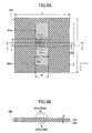
Figs. 4A and 4B show theelement cell 200 according to the present embodiment.Fig. 4A shows a top view (viewed from z direction) andFig. 4B shows a section view (showing a section indicated by a dashed line ofFig. 4A viewed from the A direction). - In the
element cell 200,patches substrate 202 of relative permittivity εr, wherein theelement cell 200 forms a square of L on a side. A dipole is formed by thepatches metal reflector 206 is formed on a surface opposite to the surface of thesubstrate 202 on which thepatches substrate 202 is indicated as L. The L is also a length of a side of theelement cell 200. In another embodiment, the array element may be formed as a rectangle. - For example, a thickness of the substrate is indicated as t.
- In the example shown in
Figs. 4A and 4B , a vertical length of the array element is ld, and a lateral length (width) of the array element is wd. Apredetermined gap 205 is formed between two adjacent patches. A fringe capacitor is formed between the adjacent patches by thegap 205. - In the present embodiment, the part where the two patches adjoin each other is formed like a comb-shape (207a, 207b) so that the two patches are engaged with each other while being separated by a predetermined gap. The comb-shape may be also called a meander. A gap of an almost rectangular corrugated shape is formed by arranging the two patches such that the two patches are engaged with each other while they are separated by a predetermined space. The shape of the gap is not limited to a particular shape as long as the gap is formed between the two patches. For example, the gap may be a line shape, or may be an arbitrary curve such as a sine wave shape, or may be a saw-tooth wave shape.
- In the example shown in
Figs. 4A and 4B , a vertical length of thefingers element cell 200 shown inFigs. 4A and 4B , the total number of the fingers is 11 in which the number of the fingers for thepatch 204a is 6, and the number for thepatch 204b is 5. -
Figs. 5A and 5B show an example of an array element having a value N different from that of the array element shown inFigs. 4A and 4B . In theelement cell 200 shown inFigs. 5A and 5B , the number of the fingers for thepatch 204a is 4 and the number of the fingers for thepatch 204b is 3, so that the total number is 7. -
Figs. 6, 7A and 7B show examples of dimensions of patches of theelement cell 200. -
Fig. 6 shows an example of dimensions of theelement cell 200 shown inFigs. 4A and 4B . The frequency of the incident wave is 24 GHz. As shown inFig. 6 , as a design example of theelement cell 200 when the incident wave is 24 GHz, L is 5.0[mm], ld is 4.0 [mm], wd is 1.2 [mm], s is 0.05 [mm], t is 0.75[mm] and εr is 2.5. -
Fig. 7A shows an example of dimensions of theelement cell 200 shown inFigs. 5A and 5B . The frequency of the incident wave is 12 GHz. As shown inFig. 7A , as a design example of theelement cell 200 when the incident wave is 12 GHz, L is 10.0[mm], ld is 8.0[mm], wd is 2.6[mm], s is 0.2[mm], t is 1.6[mm] and εr is 2.5. -
Fig. 7B shows an example of dimensions of theelement cell 200 shown inFigs. 5A and 5B . The frequency of the incident wave is 3 GHz. As shown inFig. 7B , as a design example of theelement cell 200 when the incident wave is 3 GHz, L is 40.0[mm], ld is 32.0 [mm], wd is 9. 6 [mm] , s is 0.4[mm], t is 6.0[mm] and εr is 2.5. -
Figs. 8-10 shows relationship between the phase (degrees) of the reflection coefficient (which can be also called as Reflection Phase) and the vertical length ls of the fingers (207a, 207b) of the patch. InFigs. 8-10 , the vertical length ls of the fingers (207a, 207b) of the patch is represented as "Length of fingers (ls, mm)".Figs. 8-10 show a case where a planar wave vertically enters a surface of thearray element 200. As to the frequency of the incident wave,Fig. 8 shows a case of 24 GHz,Fig. 9 shows a case of 3 GHz, andFig. 10 shows a case of 12 GHz. The numbers N of fingers (207a, 207b) are 11, 11 and 7 inFigs. 8, 9 and10 respectively. The values of ws are 0.06[mm], 0.5[mm] and 0.2[mm] inFigs. 8, 9 and10 respectively. The values of t are 0.75 mm, 6 mm and 1.6 mm inFigs. 8, 9 and10 respectively. - As the vertical length ls of the fingers (207a, 207b) of the patch increases, the length of the gap of the almost rectangular corrugated shape between the two adjacent patches increases. In other words, the longer ls becomes, the larger the surface area of the part where the adjacent patches adjoin each other becomes.
- By varying the length ls of the fingers, the surface area of each patch that forms the gap between the adjacent patches can be varied. The gap corresponds to a loaded load of scattering elements. The gap can be also changed by the lateral length (width) of the finger (207a, 207b) of the comb-shape.
- According to the
element cell 200 of the present embodiment, since the vertical length ls and/or the lateral length (width) ws of the finger (207a, 207b) of the comb-shape of the patches can be varied in a wide range, a load impedance can be adjusted in a wide range. Since the load impedance can be varied in a wide range, it becomes possible to increase the range within which the phase of the reflection coefficient can be adjusted. - As to the
element cell 200 of the present embodiment, an example is shown in which the part where the two patches face each other is formed as a comb-shape. According to the present embodiment in which the comb-shape is formed, by varying the length ls of the fingers of the comb-shape, the surface area of each patch that forms the gap between the adjacent patches can be easily varied. Also, processing for fabrication is easy. -
Figs. 8-10 show that a wide phase range of reflection coefficient can be obtained by adjusting the vertical length ls. More particularly, there is a case where equal to or greater than 1000 degrees can be obtained as the phase range of the reflection coefficient. - The phase of the reflection coefficient may vary according to a frequency to be used and an incident angle.
-
Fig. 11 shows relationship between the phase of the reflection coefficient and the vertical length ls of the fingers (207a, 207b) of the comb-shape of the patch for different frequencies of incident wave.Fig. 11 shows cases in which the frequencies of the incident wave are 23 GHz, 24 GHz and 25 GHz. - According to
Fig. 11 , in each of the cases of 23 GHz, 24 GHz and 25 GHz, equal to or greater than 1000 degrees can be obtained as the phase range of the reflection coefficient, which indicates that, the reflectarray of the present embodiment can operate in a wide band by designing the reflectarray in consideration of the band. -
Fig. 12 shows relationship between the phase of the reflection coefficient and the vertical length ls of the fingers of the comb-shape of the patch for different incident angles.Fig. 12 shows cases in which the incident angles are 30 degrees, 45 degrees and 60 degrees. The incident wave is 24 GHz. - According to
Fig. 12 , it can be understood that, since an influence of oblique incidence is not large, the influence can be neglected depending on the size of the reflectarray. However, when the size of the reflectarray becomes large to some extent, it is preferable to consider the influence. -
Fig. 13 shows a design example (1) of a reflectarray. - In the reflectarray shown in
Fig. 13 , similarly to the reflectarray shown inFig. 3 , array elements are arranged two-dimensionally in which 7 array elements are arranged in the X direction and 4 array elements are arranged in the Y direction. In this case, the incident wave is 24 GHz. The size of the reflectarray is 35[mm] in the X direction and is 20 [mm] in the Y direction. The value of t is 0.75 mm. The sizes of each array are almost the same. - Regarding the reflectarray shown in
Fig. 13 , in the vertical lines, in other words, in the array elements arranged in the X direction, the vertical length ls of the fingers of the comb-shape is different between adjacent array elements. Each of the numerical values shown in the left side ofFig. 13 indicates the vertical length ls [mm] of the fingers of the comb-shape of a corresponding array element. - In the lateral lines, in other words, in the array elements arranged in the Y direction, the vertical length ls of the fingers of the comb-shape is the same between adjacent array elements.
- Each vertical length of the fingers of the comb-shape shown in the figure is merely an example, and the length is changeable as necessary. For example, the reflectarray may be configured such that the vertical length ls of the fingers is the same between array elements adjacent in the X direction, and that the vertical length ls of the fingers is different between array elements adjacent in the Y direction. Also, the length may be different between at least a part of array elements and other array elements. Also, the length may be the same in all of the array elements.
- Since the main beam is scanned only in the X-Z plane, the reflectarray is configured such that the vertical length ls of the fingers is different between adjacent array elements arranged in the X direction, and that the vertical length ls of the fingers is the same between adjacent array elements arranged in the Y direction.
-
Fig. 14 shows an example of design dimensions and compensation phase (degree) of thereflectarray 100 shown inFig. 13 . - According to
Fig. 14 , the phase compensated between the array elements that are adjacent in the X direction is about 120 degree. -
Fig. 15 shows an example of a radiation pattern of thereflectarray 100 of the present embodiment. When the incident wave is 3 GHz, directivity becomes the maximum. The directivity is 14.1 [dBi]. The direction in which the directivity becomes the maximum is 58 degrees while the design value is 60 degrees, which indicates that difference from the design value of the 58 degrees is small. -
Fig. 16 shows a design example (2) of a reflectarray. - In the reflectarray shown in
Fig. 16 , similarly to the reflectarray shown inFig. 3 , array elements are arranged two-dimensionally in which 7 array elements are arranged in the X direction and 4 array elements are arranged in the Y direction. In this case, the incident wave is 3 GHz. The size of the reflectarray is 280 [mm] in the X direction and is 160 [mm] in the Y direction. The value of t is 6 mm. The sizes of each array element are almost the same. - Regarding the reflectarray shown in
Fig. 16 , in the vertical lines, in other words, in the array elements arranged in the X direction, the vertical length ls of the fingers of the comb-shape is different between adjacent array elements. Each of the numerical values shown in the left side ofFig. 16 indicates the vertical length ls [mm] of the fingers of the comb-shape of a corresponding array element. - In the lateral lines, in other words, in the array elements arranged in the Y direction, the vertical length ls of the fingers of the comb-shape is the same between adjacent array elements.
- Each vertical length of the fingers shown in the figure is merely an example, and the length is changeable as necessary. For example, the reflectarray may be configured such that the vertical length ls of the fingers is the same between array elements adjacent in the X direction, and that the vertical length ls of the fingers is different between array elements adjacent in the Y direction. Also, the length may be different between at least a part of array elements and other array elements. Also, the length may be the same in all of the array elements.
- Since the main beam is scanned only in the X-Z plane, the reflectarray is configured such that the vertical length ls of the fingers is different between adjacent array elements arranged in the X direction, and that the vertical length ls of the fingers is the same between adjacent array elements arranged in the Y direction.
-
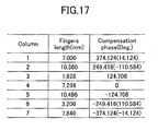
Fig. 17 shows an example of design dimensions and compensation phase (degrees) of the reflectarray shown inFig. 16 . - According to
Fig. 17 , the phase compensated between the array elements that are adjacent in the X direction is about 120 degrees. -
Fig. 18 shows a design example (3) of a reflectarray. - In the reflectarray shown in
Fig. 18 , different from the reflectarray shown inFig. 3 , array elements are arranged two-dimensionally in which 11 array elements are arranged in the X direction and 6 array elements are arranged in the Y direction. In this case, the incident wave is 12 GHz. The size of the reflectarray is 110 [mm] in the X direction and is 60 [mm] in the Y direction. The value of t is 1.6 mm. The sizes of each array are almost the same. - Regarding the reflectarray shown in
Fig. 18 , in the vertical lines, in other words, in the array elements arranged in the X direction, the vertical length ls of the fingers of the comb-shape is different between adjacent array elements. Each of the numerical values shown in the left side ofFig. 18 indicates the vertical length ls [mm] of the fingers of the comb-shape of a corresponding array element. - In the lateral lines, in other words, in the array elements arranged in the Y direction, the vertical length ls of the fingers of the comb-shape is the same between adjacent array elements.
- Each vertical length of the fingers of the comb-shape shown in the figure is merely an example, and the length is changeable as necessary. For example, the reflectarray may be configured such that the vertical length ls of the fingers is the same between array elements adjacent in the X direction, and that the vertical length ls of the fingers is different between array elements adjacent in the Y direction. Also, the length may be different between at least a part of array elements and other array elements. Also, the length may be the same in all of the array elements.
- Since the main beam is scanned only in the X-z plane, the reflectarray is configured such that the vertical length ls of the fingers of the comb-shape is different between adjacent array elements arranged in the X direction, and that the vertical length ls of the fingers of the comb-shape is the same between adjacent array elements arranged in the Y direction.
-
Fig. 19 shows an example of design dimensions and compensation phase (degrees) of the reflectarray shown inFig. 18 . - According to
Fig. 19 , the phase compensated between the array elements that are adjacent in the X direction is about 120 degrees. -
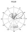
Fig. 20 shows an example of a radiation pattern of thereflectarray 100 of the present embodiment. The incident wave is 12 GHz, and the directivity gain is 17 [dBi]. The direction in which the directivity becomes the maximum is 58 degrees while the design value is 60 degrees, which indicates that difference from the design value of the 58 degrees is small. - According to the element cell of the present embodiment, by adjusting the gap formed between the adjacent patches, a load impedance can be adjusted in a wide range. Since the load impedance can be adjusted in a wide range, it becomes possible to widen the range within which the phase of the reflection coefficient can be adjusted. In the element cell, since it becomes possible to widen the range within which the phase of the reflection coefficient can be adjusted, it also becomes possible to widen the range within which the phase of the reflection coefficient can be adjusted in a reflectarray where a plurality of element cells are arranged. More particularly, by varying the vertical length ls and/or the lateral length (width) ws of the fingers (207a, 207b) of the comb-shape of the patches, a load impedance can be adjusted in a wide range. Since the load impedance can be adjusted in a wide range, it becomes possible to widen the range within which the phase of the reflection coefficient can be adjusted.
- According to the element cell of the present embodiment, by adjusting the gap formed between the adjacent patches, it becomes possible to widen the range within which the phase of the reflection coefficient can be adjusted. Therefore, in a reflectarray where a plurality of element cells are arranged, it becomes possible to widen the range within which the phase of the reflection coefficient can be adjusted without varying the size of each array element. Since it is not necessary to vary the size of the array element, characteristic deterioration of the reflectarray can be decreased, the characteristic deterioration being caused by variations of spaces between adjacent array elements.
- The reflectarray of the present modified example is similar to reflectarrays shown in
Figs. 3 and13 . - In the following, an element cell according to the present modified example is described.
-
Figs. 21A and 21B show anelement cell 200 according to the present modified embodiment.Fig. 21A shows a top view (viewed from z direction) andFig. 21B shows a section view (a section indicated by a dashed line inFig. 21A viewed from the A direction). - In the
element cell 200,patches substrate 202. Ametal reflector 206 is formed on a surface opposite to the surface of thesubstrate 202 on which thepatches - For example, the
substrate 202 is formed by a dielectric. A relative permittivity of thesubstrate 202 is represented by εr. A thickness of thesubstrate 202 is indicated as t. - In the example shown in
Figs. 21A and 21B , a vertical length of the array element is ld, and a lateral length (width) of the array element is wd. A predetermined gap is formed between two adjacent patches. A fringe capacitor is formed between the adjacent patches by the gap. - In the
element cell 200 of the present modified example, the part where two patches adjoin each other is formed like a comb-shape (207c, 207b, 207e, 207f) so that the two patches are engaged with each other while being separated by a predetermined interval. Thus, a gap of an almost rectangular corrugated shape is formed. The shape of the gap is not limited to the shape shown in the figure as long as the gap is formed between the two patches. For example, the gap may be a line shape, or may be an arbitrary curve such as a sine wave shape, or may be a saw-tooth wave shape. - As to the example shown in
Figs. 21A and 21B , in thepatch 204a and thepatch 204b that is adjacent to thepatch 204a, a vertical length of thefingers gap 2051 between adjacent fingers of the two patches is represented by s1. Therefore, a pitch of the comb-shape of a patch is represented by 2(ws1+s1). The pitch indicates a sum of the gap between the adjacent fingers and the width of the finger of the comb-shape. Also, wsl={wd-(N-1) s1}/N holds true, in which N indicates the number of fingers. As to thearray element 200 shown inFigs. 21A and 21B , the total number of the fingers is 11 in which the number of the fingers for thepatch 204a is 6, and the number for thepatch 204b adjacent to thepatch 204a is 5. The value of s1 indicates an interval between adjacent fingers. - Also, in the
patch 204b and thepatch 204c that is adjacent to thepatch 204b, a vertical length of thefingers gap 2052 between the adjacent fingers of the two patches is represented by s2. Therefore, a pitch of the comb-shape of a patch is represented by 2 (ws2+s2) . The pitch indicates a sum of the gap between the adjacent fingers and the width of a finger of the comb-shape. Also, ws2=(wd- (N-1) s2)/N2 holds true, in which N2 indicates the number of fingers. As to theelement cell 200 shown inFigs. 21A and 21B , the total number of the fingers is 11 in which the number of the fingers for thepatch 204b is 6, and the number for thepatch 204c adjacent to thepatch 204b is 5. The value of s2 indicates an interval between adjacent fingers. N and N2 may be the same or may be different. - The lengths ls1 and ls2 of the fingers may be the same or may be different. Also, the lateral lengths (widths) ws1 and ws2 of the fingers may be the same or may be different. Also, the gaps S1 and S2 between adjacent fingers of two patches may be the same or may be different.
- In the present modified example, although a case where the number of gaps between patches formed on the
element cell 200 is 2 is described, the number may be equal to or more than 3. In the case when the number of gaps between patches is equal to or more than 3, the shape of each gap may be the same or may be different. - The reflectarray of the present modified example is similar to reflectarrays shown in
Figs. 3 and13 . - In the following, an
element cell 200 according to the present modified example is described. -
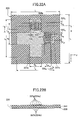
Figs. 22A and 22B show anelement cell 200 according to the present modified embodiment.Fig. 22A shows a top view (viewed from z direction) andFig. 22B shows a section view (a section indicated by a dashed line inFig. 22A viewed from the A direction). In the above-mentioned embodiments and modified example, the shape of the dipole is not limited to a rectangle. As an example of a shape other than the rectangle, a case is described in which the shape of the dipole is configured to be a cross shape. - In the
element cell 200,patches substrate 202. Ametal reflector 206 is formed on a surface opposite to the surface of thesubstrate 202 on which thepatches element cell 200 is indicated as L. - For example, the
substrate 202 is formed by a dielectric. A relative permittivity of thesubstrate 202 is represented by εr. A thickness of thesubstrate 202 is represented by t. - In the example shown in
Figs. 22A and 22B , the dipole has a shape in which parts of two patches overlap, wherein a vertical length of each patch is ld, and a lateral length (width) of each patch is wd. A predetermined gap is formed between two adjacent patches. A fringe capacitor is formed between the adjacent patches by the gap. - In the
element cell 200 of the present modified example, the part where two patches adjoin each other is formed like a comb-shape (207g, 207h, 207i, 207j) so that the two patches are engaged with each other while being separated by a predetermined space. A gap of an almost rectangular corrugated shape is formed by arranging the two patches such that the two patches are engaged with each other while they are separated by a predetermined space. The shape of the gap is not limited to the shape shown in the figure as long as the gap is formed between the two patches. For example, the gap may be a line shape, or may be an arbitrary curve such as a sine wave shape, or may be a saw-tooth wave shape. - As to the example shown in
Figs. 22A and 22B , in thepatch 204a and thepatch 204b that is adjacent to thepatch 204a, a vertical length of thefingers gap 2053 between the adjacent fingers of the two patches is represented by s3. Therefore, a pitch of the comb-shape of a patch is represented as 2 (ws3+s13). The pitch indicates a sum of the interval between the adjacent fingers and the width of a finger of the comb-shape. Also, ws3={wd-(N-1) s3}/N2 holds true, in which N indicates the number of fingers. As to theelement cell 200 shown inFigs. 22A and 22B , the total number of the fingers is 11 in which the number of the fingers for thepatch 204a is 5, and the number for thepatch 204b adjacent to thepatch 204a is 6. The value of s3 indicates an interval between adjacent fingers. N and N2 may the same or may be different. - Also, in the
patch 204b and thepatch 204c that is adjacent to thepatch 204b, a vertical length of thefingers 207i and 207j of the comb-shape is represented by ls4, and a lateral length (width) of each finger is represented by ws4. Thegap 2054 of the adjacent fingers of the two patches is represented by s4. Therefore, a pitch of the comb-shape of a patch is represented by 2 (ws4+s4) . The pitch indicates a sum of the interval between the adjacent fingers and the width of a finger of the comb-shape. Also, ws4= {wd- (N-1) s4} /N2 holds true, in which N indicates the number of fingers. As to theelement cell 200 shown inFigs. 22A and 22B , the total number of the fingers is 11 in which the number of the fingers for thepatch 204b is 6, and the number for thepatch 204c adjacent to thepatch 204b is 5. The value of s4 indicates an interval between adjacent fingers. N and N2 may the same or may be different. - The lengths ls3 and ls4 of the fingers may be the same or may be different. Also, the lateral lengths (widths) ws3 and ws4 of the fingers may be the same or may be different. Also, the gaps s3 and s4 between adjacent fingers may be the same or may be different.
- In the present modified example, although a case where the number of gaps between patches formed on the
element cell 200 is 2 is described, the number may be equal to or more than 3. In the case when the number of gaps between patches is equal to or more than 3, the shape of each gap may be the same or may be different. -
Figs. 23A-23C show anelement cell 200 according to the present modified example. In theelement cell 200, a multilayer structure is adopted using three conductive layers and two dielectric layers. Further, a multilayer cross dipole reflectarray is configured by crossing directions of dipoles of the first conductive layer and the second conductive layer. According to the array element of the present modified example, a cross dipole reflectarray can be realized that can vary phases without varying the size of patches. -
Figs. 24A and 24B show an array element according to an embodiment of the present invention. The array element is an example in which a metal reflector is not used. - According to the present embodiment and the modified examples, a reflectarray is realized.
- The reflectarray, includes:
- a substrate; and
- a plurality of patches formed on each of areas into which a principal surface of the substrate is divided,
- wherein the plurality of patches are formed by including a gap.
- By adjusting the gap formed between adjacent patches, the load impedance can be adjusted in a wide range. Since the load impedance can be adjusted in a wide range, it becomes possible to widen the range within which the phase of the reflection coefficient can be adjusted.
- In the reflectarray, a shape of an edge of a patch to which another patch adjoins is a comb-shape.
- By forming the part where two patches adjoins each other to be a comb-shape, the surface area of each patch that forms the gap formed between adjacent patches can be easily varied by varying the length ls of the finger. Also, processing becomes easy.
- In the reflectarray, a height and/or a width of a finger of the comb-shape in at least a part of the plurality of patches is different from another patch of the plurality of patches.
- By adjusting the gap formed between adjacent patches, the load impedance can be adjusted further in a wide range. Since the load impedance can be adjusted in a wide range, it becomes possible to further widen the range within which the phase of the reflection coefficient can be adjusted.
- In the reflectarray, at least one of a size of the gap, a shape of the gap, a length of the gap, a width of the gap and a ratio between the length and the width of the gap of the plurality of patches formed in at least a part of the areas is different from corresponding one of the plurality of patches formed in another area.
- Accordingly, the phase of the reflection coefficient can be varied between element cells.
- In the reflectarray, a size of the plurality of patches is the same in each of the areas.
- Accordingly, the deterioration of characteristics of the reflectarray can be reduced, wherein the deterioration is caused by variation of sizes between adjacent array elements.
- The reflectarray may further includes a metal plate that is formed on a surface opposite to the principal surface and that functions as a reflector.
- Although the present invention has been described with reference to specific embodiments, these embodiments are simply illustrative, and various variations, modifications, alterations, substitutions and so on could be conceived by those skilled in the art. The present invention has been described using specific numerals in order to facilitate understandings of the present invention, but unless specifically stated otherwise, these numerals are simply illustrative, and any other appropriate value may be used. The present invention has been described using specific equations in order to facilitate understandings of the present invention, but unless specifically stated otherwise, these equations are simply illustrative, and any other appropriate equations may be used. Classification into each embodiment or each item is not essential in the present invention, and matters described in equal to or more than two embodiments or items may be combined and used as necessary. Also, a matter described in an embodiment or item may be applied to another matter described in another embodiment or item unless they are contradictory. The present invention is not limited to the above-mentioned embodiment and is intended to include various variations, modifications, alterations, substitutions and so on without departing from the spirit of the present invention.
Claims (6)
- A reflectarray, comprising:a substrate; anda plurality of patches formed on each of areas into which a principal surface of the substrate is divided,wherein the plurality of patches are formed by including a gap.
- The reflectarray as claimed in claim 1, wherein, for each of the plurality of patches, a shape of an edge of a patch to which another patch adjoins is a comb-shape.
- The reflectarray as claimed in claim 2, wherein, a height and/or a width of a finger of the comb-shape in at least a part of the plurality of patches is different from another patch of the plurality of patches.
- The reflectarray as claimed in any one of claims 1 - 3, wherein at least one of a size of the gap, a shape of the gap, a length of the gap, a width of the gap and a ratio between the length and the width of the gap of the plurality of patches formed in at least a part of the areas is different from corresponding one of the plurality of patches formed in another area.
- The reflectarray as claimed in any one of claims 1 - 4, wherein a size of the plurality of patches is the same in each of the areas.
- The reflectarray as claimed in any one of claims 1 - 5, comprising a metal plate that is formed on a surface opposite to the principal surface and that functions as a reflector.
Applications Claiming Priority (1)
| Application Number | Priority Date | Filing Date | Title |
|---|---|---|---|
| JP2010191568A JP5177708B2 (en) | 2010-08-27 | 2010-08-27 | Reflect array |
Publications (2)
| Publication Number | Publication Date |
|---|---|
| EP2424038A1 true EP2424038A1 (en) | 2012-02-29 |
| EP2424038B1 EP2424038B1 (en) | 2017-01-11 |
Family
ID=44651195
Family Applications (1)
| Application Number | Title | Priority Date | Filing Date |
|---|---|---|---|
| EP11179107.5A Active EP2424038B1 (en) | 2010-08-27 | 2011-08-26 | Reflectarray |
Country Status (4)
| Country | Link |
|---|---|
| US (1) | US8836583B2 (en) |
| EP (1) | EP2424038B1 (en) |
| JP (1) | JP5177708B2 (en) |
| CN (1) | CN102437434B (en) |
Families Citing this family (7)
| Publication number | Priority date | Publication date | Assignee | Title |
|---|---|---|---|---|
| KR102175681B1 (en) | 2014-11-20 | 2020-11-06 | 삼성전자주식회사 | Reradiate repeater |
| US10938116B2 (en) | 2017-05-18 | 2021-03-02 | Samsung Electronics Co., Ltd. | Reflector for changing directionality of wireless communication beam and apparatus including the same |
| JP7327465B2 (en) | 2019-03-15 | 2023-08-16 | Agc株式会社 | Radio communication equipment |
| CN118715673A (en) | 2022-01-19 | 2024-09-27 | 日东电工株式会社 | Reflector |
| WO2023188735A1 (en) * | 2022-03-30 | 2023-10-05 | 株式会社ジャパンディスプレイ | Radio wave reflective element using liquid crystal material |
| JP7384308B1 (en) * | 2023-03-03 | 2023-11-21 | Toppanホールディングス株式会社 | Reflect array, reflect array device, and reflect array design method |
| KR20250153234A (en) | 2023-03-31 | 2025-10-24 | 닛토덴코 가부시키가이샤 | reflector |
Citations (1)
| Publication number | Priority date | Publication date | Assignee | Title |
|---|---|---|---|---|
| US20030142036A1 (en) * | 2001-02-08 | 2003-07-31 | Wilhelm Michael John | Multiband or broadband frequency selective surface |
Family Cites Families (13)
| Publication number | Priority date | Publication date | Assignee | Title |
|---|---|---|---|---|
| JPS60251707A (en) | 1984-05-29 | 1985-12-12 | Nec Corp | Microstrip array type reflecting plate |
| JP3390503B2 (en) * | 1993-11-26 | 2003-03-24 | 株式会社日立国際電気 | Dual-polarized antenna |
| JP3107150B2 (en) * | 1997-04-11 | 2000-11-06 | 日本電気株式会社 | Crossed finger print antenna |
| US6642889B1 (en) * | 2002-05-03 | 2003-11-04 | Raytheon Company | Asymmetric-element reflect array antenna |
| US6822616B2 (en) * | 2002-12-03 | 2004-11-23 | Harris Corporation | Multi-layer capacitive coupling in phased array antennas |
| WO2004109851A1 (en) * | 2003-05-30 | 2004-12-16 | Raytheon Company | Monolithic millmeter wave reflect array system |
| US6876336B2 (en) * | 2003-08-04 | 2005-04-05 | Harris Corporation | Phased array antenna with edge elements and associated methods |
| US6927745B2 (en) * | 2003-08-25 | 2005-08-09 | Harris Corporation | Frequency selective surfaces and phased array antennas using fluidic dielectrics |
| JP4744949B2 (en) * | 2005-06-24 | 2011-08-10 | 三菱電機株式会社 | Radio wave shielding device |
| JP4557169B2 (en) * | 2005-10-03 | 2010-10-06 | 株式会社デンソー | antenna |
| TW200807809A (en) * | 2006-07-28 | 2008-02-01 | Tatung Co Ltd | Microstrip reflection array antenna |
| FR2936906B1 (en) | 2008-10-07 | 2011-11-25 | Thales Sa | OPTIMIZED ARRANGEMENT REFLECTOR NETWORK AND ANTENNA HAVING SUCH A REFLECTIVE NETWORK |
| JP2011019021A (en) | 2009-07-07 | 2011-01-27 | Ntt Docomo Inc | Reflect array |
-
2010
- 2010-08-27 JP JP2010191568A patent/JP5177708B2/en active Active
-
2011
- 2011-08-24 CN CN201110246689.2A patent/CN102437434B/en active Active
- 2011-08-24 US US13/216,451 patent/US8836583B2/en active Active
- 2011-08-26 EP EP11179107.5A patent/EP2424038B1/en active Active
Patent Citations (1)
| Publication number | Priority date | Publication date | Assignee | Title |
|---|---|---|---|---|
| US20030142036A1 (en) * | 2001-02-08 | 2003-07-31 | Wilhelm Michael John | Multiband or broadband frequency selective surface |
Non-Patent Citations (5)
| Title |
|---|
| J. HUANG, J. A. ENCINAR: "Reflectarray antennas", 2008, IEEE PRESS; WILEY-INTERSCIENCE |
| JIANFENG LI ET AL: "Reflectarray design based on interdigital gap loading element", WIRELESS INFORMATION TECHNOLOGY AND SYSTEMS (ICWITS), 2010 IEEE INTERNATIONAL CONFERENCE ON, IEEE, PISCATAWAY, NJ, USA, 28 August 2010 (2010-08-28), pages 1 - 4, XP031782522, ISBN: 978-1-4244-7091-4 * |
| L. LI ET AL.: "Microstrip reflectarray using crossed-dipole with frequency selective surface of loops", ISAP2008, 2008 |
| POZAR D M: "Wideband reflectarrays using artificial impedance surfaces", ELECTRONICS LETTERS, IEE STEVENAGE, GB, vol. 43, no. 3, 1 February 2007 (2007-02-01), pages 148 - 149, XP006028166, ISSN: 0013-5194, DOI: 10.1049/EL:20073560 * |
| T. MARUYAMA, T. FURUNO, S. UEBAYASHI: "Experiment and analysis of reflect beam direction control using a reflector having periodic tapered mushroom-like structure", ISAP2008, pages 9 |
Also Published As
| Publication number | Publication date |
|---|---|
| JP2012049931A (en) | 2012-03-08 |
| JP5177708B2 (en) | 2013-04-10 |
| CN102437434B (en) | 2015-03-04 |
| US20120050127A1 (en) | 2012-03-01 |
| EP2424038B1 (en) | 2017-01-11 |
| US8836583B2 (en) | 2014-09-16 |
| CN102437434A (en) | 2012-05-02 |
Similar Documents
| Publication | Publication Date | Title |
|---|---|---|
| EP2424038B1 (en) | Reflectarray | |
| CN107437659B (en) | Apparatus and method for reducing mutual coupling in antenna arrays | |
| US8350759B2 (en) | Antenna having metamaterial superstrate and providing gain improvement and beamforming together | |
| EP2415119B1 (en) | Wide band array antenna | |
| US6919854B2 (en) | Variable inclination continuous transverse stub array | |
| CN110994194A (en) | Antenna unit, array antenna and radar system | |
| US8736514B2 (en) | Antenna | |
| EP3972050A1 (en) | Antenna assembly and electronic device | |
| EP3993164A1 (en) | Antenna assembly and electronic device | |
| CN113161715B (en) | Display substrate and method for manufacturing the same | |
| US20100164827A1 (en) | Dielectric antenna | |
| CN110957585A (en) | A Planar Reflective Array Antenna Based on Liquid Crystal Materials | |
| CN106505310B (en) | Low section array antenna with broadband and wide angle scan characteristic | |
| CN109904592B (en) | An antenna structure and communication terminal | |
| CN115764288A (en) | Dual-polarized one-dimensional linear array wide-angle scanning array antenna and electronic equipment | |
| US20090160729A1 (en) | Antenna array with reduced electromagnetic coupling | |
| JP2012049654A (en) | Ebg structure by divided substrate | |
| US10547105B2 (en) | Superstrate polarization and impedance rectifying elements | |
| US20160043464A1 (en) | Ground Plane Meandering in Z Direction for Spiral Antenna | |
| US20090207089A1 (en) | Antenna element | |
| JP2009218993A (en) | Antenna device and array antenna | |
| JP7514736B2 (en) | Antenna Device | |
| JP5050084B2 (en) | antenna | |
| Arand et al. | Gain enhancement of a tetra-band square-loop patch antenna using an AMC–PEC substrate and a superstrate | |
| Khattak et al. | Surface Wave Launcher Based Multi-beam Antenna for 5G Applications |
Legal Events
| Date | Code | Title | Description |
|---|---|---|---|
| 17P | Request for examination filed |
Effective date: 20110826 |
|
| AK | Designated contracting states |
Kind code of ref document: A1 Designated state(s): AL AT BE BG CH CY CZ DE DK EE ES FI FR GB GR HR HU IE IS IT LI LT LU LV MC MK MT NL NO PL PT RO RS SE SI SK SM TR |
|
| AX | Request for extension of the european patent |
Extension state: BA ME |
|
| PUAI | Public reference made under article 153(3) epc to a published international application that has entered the european phase |
Free format text: ORIGINAL CODE: 0009012 |
|
| 17Q | First examination report despatched |
Effective date: 20150227 |
|
| GRAP | Despatch of communication of intention to grant a patent |
Free format text: ORIGINAL CODE: EPIDOSNIGR1 |
|
| INTG | Intention to grant announced |
Effective date: 20160926 |
|
| GRAS | Grant fee paid |
Free format text: ORIGINAL CODE: EPIDOSNIGR3 |
|
| GRAA | (expected) grant |
Free format text: ORIGINAL CODE: 0009210 |
|
| AK | Designated contracting states |
Kind code of ref document: B1 Designated state(s): AL AT BE BG CH CY CZ DE DK EE ES FI FR GB GR HR HU IE IS IT LI LT LU LV MC MK MT NL NO PL PT RO RS SE SI SK SM TR |
|
| REG | Reference to a national code |
Ref country code: GB Ref legal event code: FG4D |
|
| REG | Reference to a national code |
Ref country code: CH Ref legal event code: EP |
|
| REG | Reference to a national code |
Ref country code: AT Ref legal event code: REF Ref document number: 862050 Country of ref document: AT Kind code of ref document: T Effective date: 20170115 |
|
| REG | Reference to a national code |
Ref country code: IE Ref legal event code: FG4D |
|
| REG | Reference to a national code |
Ref country code: DE Ref legal event code: R096 Ref document number: 602011034225 Country of ref document: DE |
|
| REG | Reference to a national code |
Ref country code: LT Ref legal event code: MG4D |
|
| REG | Reference to a national code |
Ref country code: NL Ref legal event code: MP Effective date: 20170111 |
|
| REG | Reference to a national code |
Ref country code: AT Ref legal event code: MK05 Ref document number: 862050 Country of ref document: AT Kind code of ref document: T Effective date: 20170111 |
|
| PG25 | Lapsed in a contracting state [announced via postgrant information from national office to epo] |
Ref country code: NL Free format text: LAPSE BECAUSE OF FAILURE TO SUBMIT A TRANSLATION OF THE DESCRIPTION OR TO PAY THE FEE WITHIN THE PRESCRIBED TIME-LIMIT Effective date: 20170111 |
|
| PG25 | Lapsed in a contracting state [announced via postgrant information from national office to epo] |
Ref country code: IS Free format text: LAPSE BECAUSE OF FAILURE TO SUBMIT A TRANSLATION OF THE DESCRIPTION OR TO PAY THE FEE WITHIN THE PRESCRIBED TIME-LIMIT Effective date: 20170511 Ref country code: FI Free format text: LAPSE BECAUSE OF FAILURE TO SUBMIT A TRANSLATION OF THE DESCRIPTION OR TO PAY THE FEE WITHIN THE PRESCRIBED TIME-LIMIT Effective date: 20170111 Ref country code: HR Free format text: LAPSE BECAUSE OF FAILURE TO SUBMIT A TRANSLATION OF THE DESCRIPTION OR TO PAY THE FEE WITHIN THE PRESCRIBED TIME-LIMIT Effective date: 20170111 Ref country code: LT Free format text: LAPSE BECAUSE OF FAILURE TO SUBMIT A TRANSLATION OF THE DESCRIPTION OR TO PAY THE FEE WITHIN THE PRESCRIBED TIME-LIMIT Effective date: 20170111 Ref country code: NO Free format text: LAPSE BECAUSE OF FAILURE TO SUBMIT A TRANSLATION OF THE DESCRIPTION OR TO PAY THE FEE WITHIN THE PRESCRIBED TIME-LIMIT Effective date: 20170411 Ref country code: GR Free format text: LAPSE BECAUSE OF FAILURE TO SUBMIT A TRANSLATION OF THE DESCRIPTION OR TO PAY THE FEE WITHIN THE PRESCRIBED TIME-LIMIT Effective date: 20170412 |
|
| PG25 | Lapsed in a contracting state [announced via postgrant information from national office to epo] |
Ref country code: PT Free format text: LAPSE BECAUSE OF FAILURE TO SUBMIT A TRANSLATION OF THE DESCRIPTION OR TO PAY THE FEE WITHIN THE PRESCRIBED TIME-LIMIT Effective date: 20170511 Ref country code: BG Free format text: LAPSE BECAUSE OF FAILURE TO SUBMIT A TRANSLATION OF THE DESCRIPTION OR TO PAY THE FEE WITHIN THE PRESCRIBED TIME-LIMIT Effective date: 20170411 Ref country code: RS Free format text: LAPSE BECAUSE OF FAILURE TO SUBMIT A TRANSLATION OF THE DESCRIPTION OR TO PAY THE FEE WITHIN THE PRESCRIBED TIME-LIMIT Effective date: 20170111 Ref country code: LV Free format text: LAPSE BECAUSE OF FAILURE TO SUBMIT A TRANSLATION OF THE DESCRIPTION OR TO PAY THE FEE WITHIN THE PRESCRIBED TIME-LIMIT Effective date: 20170111 Ref country code: AT Free format text: LAPSE BECAUSE OF FAILURE TO SUBMIT A TRANSLATION OF THE DESCRIPTION OR TO PAY THE FEE WITHIN THE PRESCRIBED TIME-LIMIT Effective date: 20170111 Ref country code: ES Free format text: LAPSE BECAUSE OF FAILURE TO SUBMIT A TRANSLATION OF THE DESCRIPTION OR TO PAY THE FEE WITHIN THE PRESCRIBED TIME-LIMIT Effective date: 20170111 Ref country code: SE Free format text: LAPSE BECAUSE OF FAILURE TO SUBMIT A TRANSLATION OF THE DESCRIPTION OR TO PAY THE FEE WITHIN THE PRESCRIBED TIME-LIMIT Effective date: 20170111 Ref country code: PL Free format text: LAPSE BECAUSE OF FAILURE TO SUBMIT A TRANSLATION OF THE DESCRIPTION OR TO PAY THE FEE WITHIN THE PRESCRIBED TIME-LIMIT Effective date: 20170111 |
|
| REG | Reference to a national code |
Ref country code: DE Ref legal event code: R097 Ref document number: 602011034225 Country of ref document: DE |
|
| PG25 | Lapsed in a contracting state [announced via postgrant information from national office to epo] |
Ref country code: SK Free format text: LAPSE BECAUSE OF FAILURE TO SUBMIT A TRANSLATION OF THE DESCRIPTION OR TO PAY THE FEE WITHIN THE PRESCRIBED TIME-LIMIT Effective date: 20170111 Ref country code: RO Free format text: LAPSE BECAUSE OF FAILURE TO SUBMIT A TRANSLATION OF THE DESCRIPTION OR TO PAY THE FEE WITHIN THE PRESCRIBED TIME-LIMIT Effective date: 20170111 Ref country code: IT Free format text: LAPSE BECAUSE OF FAILURE TO SUBMIT A TRANSLATION OF THE DESCRIPTION OR TO PAY THE FEE WITHIN THE PRESCRIBED TIME-LIMIT Effective date: 20170111 Ref country code: CZ Free format text: LAPSE BECAUSE OF FAILURE TO SUBMIT A TRANSLATION OF THE DESCRIPTION OR TO PAY THE FEE WITHIN THE PRESCRIBED TIME-LIMIT Effective date: 20170111 Ref country code: EE Free format text: LAPSE BECAUSE OF FAILURE TO SUBMIT A TRANSLATION OF THE DESCRIPTION OR TO PAY THE FEE WITHIN THE PRESCRIBED TIME-LIMIT Effective date: 20170111 |
|
| PLBE | No opposition filed within time limit |
Free format text: ORIGINAL CODE: 0009261 |
|
| STAA | Information on the status of an ep patent application or granted ep patent |
Free format text: STATUS: NO OPPOSITION FILED WITHIN TIME LIMIT |
|
| PG25 | Lapsed in a contracting state [announced via postgrant information from national office to epo] |
Ref country code: DK Free format text: LAPSE BECAUSE OF FAILURE TO SUBMIT A TRANSLATION OF THE DESCRIPTION OR TO PAY THE FEE WITHIN THE PRESCRIBED TIME-LIMIT Effective date: 20170111 Ref country code: SM Free format text: LAPSE BECAUSE OF FAILURE TO SUBMIT A TRANSLATION OF THE DESCRIPTION OR TO PAY THE FEE WITHIN THE PRESCRIBED TIME-LIMIT Effective date: 20170111 |
|
| 26N | No opposition filed |
Effective date: 20171012 |
|
| PG25 | Lapsed in a contracting state [announced via postgrant information from national office to epo] |
Ref country code: SI Free format text: LAPSE BECAUSE OF FAILURE TO SUBMIT A TRANSLATION OF THE DESCRIPTION OR TO PAY THE FEE WITHIN THE PRESCRIBED TIME-LIMIT Effective date: 20170111 |
|
| REG | Reference to a national code |
Ref country code: CH Ref legal event code: PL |
|
| PG25 | Lapsed in a contracting state [announced via postgrant information from national office to epo] |
Ref country code: MC Free format text: LAPSE BECAUSE OF FAILURE TO SUBMIT A TRANSLATION OF THE DESCRIPTION OR TO PAY THE FEE WITHIN THE PRESCRIBED TIME-LIMIT Effective date: 20170111 |
|
| PG25 | Lapsed in a contracting state [announced via postgrant information from national office to epo] |
Ref country code: CH Free format text: LAPSE BECAUSE OF NON-PAYMENT OF DUE FEES Effective date: 20170831 Ref country code: LI Free format text: LAPSE BECAUSE OF NON-PAYMENT OF DUE FEES Effective date: 20170831 |
|
| REG | Reference to a national code |
Ref country code: FR Ref legal event code: ST Effective date: 20180430 |
|
| REG | Reference to a national code |
Ref country code: IE Ref legal event code: MM4A |
|
| REG | Reference to a national code |
Ref country code: BE Ref legal event code: MM Effective date: 20170831 |
|
| PG25 | Lapsed in a contracting state [announced via postgrant information from national office to epo] |
Ref country code: LU Free format text: LAPSE BECAUSE OF NON-PAYMENT OF DUE FEES Effective date: 20170826 |
|
| PG25 | Lapsed in a contracting state [announced via postgrant information from national office to epo] |
Ref country code: IE Free format text: LAPSE BECAUSE OF NON-PAYMENT OF DUE FEES Effective date: 20170826 |
|
| PG25 | Lapsed in a contracting state [announced via postgrant information from national office to epo] |
Ref country code: FR Free format text: LAPSE BECAUSE OF NON-PAYMENT OF DUE FEES Effective date: 20170831 Ref country code: BE Free format text: LAPSE BECAUSE OF NON-PAYMENT OF DUE FEES Effective date: 20170831 |
|
| PG25 | Lapsed in a contracting state [announced via postgrant information from national office to epo] |
Ref country code: MT Free format text: LAPSE BECAUSE OF NON-PAYMENT OF DUE FEES Effective date: 20170826 |
|
| PG25 | Lapsed in a contracting state [announced via postgrant information from national office to epo] |
Ref country code: HU Free format text: LAPSE BECAUSE OF FAILURE TO SUBMIT A TRANSLATION OF THE DESCRIPTION OR TO PAY THE FEE WITHIN THE PRESCRIBED TIME-LIMIT; INVALID AB INITIO Effective date: 20110826 |
|
| PG25 | Lapsed in a contracting state [announced via postgrant information from national office to epo] |
Ref country code: CY Free format text: LAPSE BECAUSE OF NON-PAYMENT OF DUE FEES Effective date: 20170111 |
|
| PG25 | Lapsed in a contracting state [announced via postgrant information from national office to epo] |
Ref country code: MK Free format text: LAPSE BECAUSE OF FAILURE TO SUBMIT A TRANSLATION OF THE DESCRIPTION OR TO PAY THE FEE WITHIN THE PRESCRIBED TIME-LIMIT Effective date: 20170111 |
|
| PG25 | Lapsed in a contracting state [announced via postgrant information from national office to epo] |
Ref country code: TR Free format text: LAPSE BECAUSE OF FAILURE TO SUBMIT A TRANSLATION OF THE DESCRIPTION OR TO PAY THE FEE WITHIN THE PRESCRIBED TIME-LIMIT Effective date: 20170111 |
|
| PG25 | Lapsed in a contracting state [announced via postgrant information from national office to epo] |
Ref country code: AL Free format text: LAPSE BECAUSE OF FAILURE TO SUBMIT A TRANSLATION OF THE DESCRIPTION OR TO PAY THE FEE WITHIN THE PRESCRIBED TIME-LIMIT Effective date: 20170111 |
|
| PGFP | Annual fee paid to national office [announced via postgrant information from national office to epo] |
Ref country code: DE Payment date: 20250820 Year of fee payment: 15 |
|
| PGFP | Annual fee paid to national office [announced via postgrant information from national office to epo] |
Ref country code: GB Payment date: 20250820 Year of fee payment: 15 |