EP2423854A1 - Noncontact information processing device and noncontact card-formed medium issuing machine - Google Patents
Noncontact information processing device and noncontact card-formed medium issuing machine Download PDFInfo
- Publication number
- EP2423854A1 EP2423854A1 EP10766825A EP10766825A EP2423854A1 EP 2423854 A1 EP2423854 A1 EP 2423854A1 EP 10766825 A EP10766825 A EP 10766825A EP 10766825 A EP10766825 A EP 10766825A EP 2423854 A1 EP2423854 A1 EP 2423854A1
- Authority
- EP
- European Patent Office
- Prior art keywords
- contact
- communication antenna
- card
- electromagnetic wave
- contact communication
- Prior art date
- Legal status (The legal status is an assumption and is not a legal conclusion. Google has not performed a legal analysis and makes no representation as to the accuracy of the status listed.)
- Granted
Links
Images



Classifications
-
- G—PHYSICS
- G06—COMPUTING OR CALCULATING; COUNTING
- G06K—GRAPHICAL DATA READING; PRESENTATION OF DATA; RECORD CARRIERS; HANDLING RECORD CARRIERS
- G06K7/00—Methods or arrangements for sensing record carriers, e.g. for reading patterns
- G06K7/10—Methods or arrangements for sensing record carriers, e.g. for reading patterns by electromagnetic radiation, e.g. optical sensing; by corpuscular radiation
- G06K7/10009—Methods or arrangements for sensing record carriers, e.g. for reading patterns by electromagnetic radiation, e.g. optical sensing; by corpuscular radiation sensing by radiation using wavelengths larger than 0.1 mm, e.g. radio-waves or microwaves
- G06K7/10366—Methods or arrangements for sensing record carriers, e.g. for reading patterns by electromagnetic radiation, e.g. optical sensing; by corpuscular radiation sensing by radiation using wavelengths larger than 0.1 mm, e.g. radio-waves or microwaves the interrogation device being adapted for miscellaneous applications
- G06K7/10465—Methods or arrangements for sensing record carriers, e.g. for reading patterns by electromagnetic radiation, e.g. optical sensing; by corpuscular radiation sensing by radiation using wavelengths larger than 0.1 mm, e.g. radio-waves or microwaves the interrogation device being adapted for miscellaneous applications the interrogation device being capable of self-diagnosis, e.g. in addition to or as part of the actual interrogation process
-
- G—PHYSICS
- G06—COMPUTING OR CALCULATING; COUNTING
- G06K—GRAPHICAL DATA READING; PRESENTATION OF DATA; RECORD CARRIERS; HANDLING RECORD CARRIERS
- G06K7/00—Methods or arrangements for sensing record carriers, e.g. for reading patterns
- G06K7/0095—Testing the sensing arrangement, e.g. testing if a magnetic card reader, bar code reader, RFID interrogator or smart card reader functions properly
Definitions
- the present invention relates a non-contact information processing device and a non-contact card medium issuing machine for recording and/or reproducing information of various kinds of card media, such as a banking card, a credit card, and the like without contacting them.
- Information to/from a magnetic card and a contact IC card is recorded and/or reproduced by a magnetic card reader equipped with a magnetic head and an IC contact.
- information to/from a non-contact IC card is recorded and/or reproduced by a non-contact card reader equipped with a non-contact communication antenna.
- a card issuing machine on which such a non-contact card reader is mounted is a non-contact card medium issuing machine that has a reading/writing function for non-contact IC cards.
- a non-contact IC card inserted through a gate hole is transferred by using a motor to a position where a non-contact communication antenna is placed, and information is sent and received through electromagnetic induction (by means of non-contact IC card communication). Then, after completion of the communication, the non-contact IC card is unloaded from the gate hole.
- a signal is sent from a non-contact control IC for controlling the function of the non-contact communication antenna through a predetermined circuit to a CPU port, while a judgment LED is separately mounted, and the judgment is made by checking an ON/OFF status of the judgment LED.
- the non-contact communication antenna is additionally equipped with its own IC tag for antenna inspection, and an ID code is exchanged between a non-contact control IC and the IC tag for antenna inspection in order to make a judgment on whether the non-contact communication antenna is working normally (for example, refer to Patent Document 1).
- the present invention provides the following aspects.
- the non-contact information processing device including the device-side non-contact communication antenna is provided with detection means that detects if the device-side non-contact communication antenna is working normally.
- the detection means has the control section, being independent of the control circuit for controlling the device-side non-contact communication antenna, and it can detect an electromagnetic wave generated from the device-side non-contact communication antenna. Therefore, it can be judged easily and quickly whether or not an electromagnetic wave radiation function of the non-contact communication antenna works properly.
- the detection means when the detection means can detect an electromagnetic wave radiated from the non-contact communication antenna, it can be recognized that the electromagnetic wave radiation function of the non-contact communication antenna is working properly. On the contrary, when the detection means cannot detect any electromagnetic wave, a maintenance personnel can quickly carry out maintenance work while paying attention to any trouble of the non-contact communication antenna.
- the detection means according to the present invention operates by means of the control section, being independent of the control circuit (for example, a non-contact control IC) for controlling the device-side non-contact communication antenna, and therefore it can fulfill an electromagnetic wave detection function, with no reference to any failure of the control circuit.
- the detection means described above is provided with the electromagnetic wave detection antenna for detecting an electromagnetic wave, and the electromagnetic wave detection LED for visually checking if the device-side non-contact communication antenna is working normally; and the control section described above is equipped with the rectifier circuit for rectifying a current obtained through the electromagnetic wave detection antenna, and supplying the rectified current to the electromagnetic wave detection LED. Therefore, the electromagnetic wave detection LED can be supplied with electric power through the rectifier circuit. As a result, neither any external power supply nor a battery is needed for operating the detection means; and by using a simpler configuration, it can be judged whether or not the electromagnetic wave radiation function of the device-side non-contact communication antenna works properly. Moreover, since such an electromagnetic wave detection LED and a rectifier circuit can be purchased at low cost, this arrangement can also contribute to production cost savings.
- the control section described above is equipped with a variable resistor for regulating the amount of current to be supplied to the electromagnetic wave detection LED. Therefore, in addition to an original purpose of preventing an excessive current flow into the electromagnetic wave detection LED, the amount of current to be supplied can be changed variably according to the electromagnetic wave strength so that brightness of the electromagnetic wave detection LED can be controlled.
- the non-contact information processing device is provided with the CPU checking LED for visually checking if the CPU (main CPU) for comprehensively controlling the whole device is working properly. Then, by means of the CPU checking LED and the above-described electromagnetic wave detection LED, it can be visually checked if the CPU and the device-side non-contact communication antenna are working properly. Therefore, a maintenance personnel can identify a defective spot further easily and quickly.
- the detection means described above is installed at a position where is not formed the electromagnetic shield placed so as to surround at least a part of the device-side non-contact communication antenna. Therefore, it is possible to prevent a detection error from happening owing to turbulence of a magnetic flux due to presence of the electromagnetic shield.
- the non-contact card medium issuing machine that makes it possible to judge easily and quickly whether or not the electromagnetic radiation function of the device-side non-contact communication antenna works properly.
- detection means for detecting if a device-side non-contact communication antenna is working normally it becomes possible to judge easily and quickly whether or not an electromagnetic wave radiation function of the device-side non-contact communication antenna works properly.
- FIG. 1 includes drawings that show a structure of a non-contact card issuing machine 100 (an example of a non-contact card medium issuing machine) according to an embodiment of the present invention.
- FIG. 1A is an external side view drawing of the non-contact card issuing machine 100, which shows a view from a left front position
- FIG. 1B is another external side view drawing of the non-contact card issuing machine 100, which shows a view from a right front position
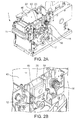
- FIG. 2A is a drawing that shows conditions of the non-contact card issuing machine 100 shown in FIG. 1B , from which a cover 102 for a chassis is removed
- FIG. 2B is an enlarged view of a part of FIG. 2A .
- FIG. 1A is an external side view drawing of the non-contact card issuing machine 100, which shows a view from a left front position
- FIG. 1B is another external side view drawing of the non-contact card issuing machine 100, which shows a view from a right front position
- FIG. 2A is
- FIG. 3A is a drawing that shows conditions of the non-contact card issuing machine 100 shown in FIG. 2A , in a view from a right rear position, while FIG. 3B is an enlarged view of a part of FIG. 3A .
- a card reader 1 Being connected to a higher-level device (for example, such as an ATM (a host apparatus), and the like), a card reader 1 receives a command from the higher-level device, and sends a command execution result and so on to the higher-level device, through a predetermined interface.
- the card reader 1 Being equipped with a magnetic head (not shown in the drawings) and a device-side non-contact communication antenna 23, the card reader 1 is a hybrid machine that can handle both a magnetic card and a non-contact IC card 'C.'
- an X-direction three directions being at right angles to one another are called an X-direction, a Y-direction, and a Z-direction; and in the meantime, an X1-direciton represents a rightward direction, and an X2-direction is a leftward direction; a Y1-direction represents a frontward direction, while a Y2-direction is a rearward direction; and a Z1-direction represents an upward direction, and a Z2-direction is a downward direction.
- the non-contact card issuing machine 100 shown in FIG. 1 through FIG. 3 is provided with a function for issuing a card stored internally, and it is installed for use, for example, at a front desk of a hotel, a cash register of a convenience store, and the like. It is also provided with a function for collecting a needless card, a used card, a defective card, and so on.
- the non-contact card issuing machine 100 includes the card reader 1 as an example of a non-contact information processing device, and a card issuing/collecting section 101 for issuing and collecting a card.
- the card reader 1 includes a card loading port 11 (which works as a card unloading port at the time of unloading a card), a transfer path through which a card is transferred in a rearward direction from the card loading port 11, a magnetic head which contacts with and slides on a magnetic stripe on a card for executing read/write operations (recording and/or reproducing information) with respect to the card, as well as the device-side non-contact communication antenna 23.
- a circuit board 22 placed under the card reader 1 is a circuit board 22 (Refer to FIG.
- the magnetic head While contacting with and sliding on a magnetic stripe on a card surface, the magnetic head reads out magnetic data recorded in the magnetic stripe, and creates a reproduced signal according to the magnetic data.
- the device-side non-contact communication antenna 23 is able to send and receive information to/from a non-contact communication antenna provided to (embedded in) the card, and the device-side non-contact communication antenna 23 communicates with an IC chip embedded in the card by means of electromagnetic induction through the non-contact communication antenna.
- the device-side non-contact communication antenna 23 is located in the vicinity of and above the transfer path, and it is controlled by a non-contact control IC 40a mounted on a control board 40.
- the card issuing/collecting section 101 has a card storage function for storing a plurality of cards that are stacked before issuance, and a card collecting function for collecting needless cards. Furthermore, the card issuing/collecting section 101 also has an unloading mechanism for delivering a stored card to the card reader 1 (not shown in the drawings). Concretely to describe, the card issuing/collecting section 101 includes a card storage section 101A for storing a plurality of cards that are stacked before issuance, and a card collecting compartment 101B for collecting needless cards.
- the card unloading mechanism delivers a card, stored in the card issuing/collecting section 101, to the card reader 1.
- the card reader 1 for example, predetermined information is recorded into the card.
- the card into which information has been recorded is unloaded (issued) from the non-contact card issuing machine 100 via the card loading port 11.
- the card In the case of a card, for example, which has been loaded into the non-contact card issuing machine 100, if it is judged that collecting the card is required as a result of information communication in the card reader 1, the card is unloaded from the card reader 1 to the card issuing/collecting section 101.
- the card unloaded from the card reader 1 is introduced to the card collecting compartment 101B by a guiding member, which is not shown in the drawings, so as to be collected there. Since the card collecting compartment 101B is located at a position lower than the card reader 1, the card unloaded from the card reader 1 drops by gravity into the card collecting compartment 101B.
- the cover 102 shown in FIG. 1B is made of resin material, and removing the cover 102 results in the conditions shown in FIG. 2A .
- rollers 12 and 16 are provided at a right side surface of the card reader 1, and placed between the rollers 12 and 16 is an electromagnetic wave detection circuit mounting plate 60 structured with resin material.
- the electromagnetic wave detection circuit mounting plate 60 is a plate component extending in each of frontward, rearward, upward, and downward directions (Y1-, Y2-, Z1-, and Z2- directions in FIG. 1 ), having its thickness in rightward and leftward directions (X1- and X2- directions in FIG. 1 ).
- the control board 40 placed above the card reader 1 is the control board 40 on which the non-contact control IC 40a is mounted for controlling the device-side non-contact communication antenna 23.
- the device-side non-contact communication antenna 23 is so installed under the control board 40 as to be in parallel with a card to be loaded.
- an electromagnetic shield 30 is so placed as to surround the device-side non-contact communication antenna 23.
- the electromagnetic shield 30 does not cover all circumferences of the device-side non-contact communication antenna 23.
- a front side, a left side, and a rear side of the device-side non-contact communication antenna 23 are covered with the electromagnetic shield 30. In other words, no electromagnetic shield is formed at a right side of the device-side non-contact communication antenna 23, and then the electromagnetic wave detection circuit mounting plate 60 described above is placed at the side.
- an electromagnetic wave detection circuit 50 is provided at a right side surface of the electromagnetic wave detection circuit mounting plate 60.
- the electromagnetic wave detection circuit 50 is a circuit that functions as an example of detection means for detecting if the device-side non-contact communication antenna 23 is working normally. A configuration of the circuit is described later.
- the electromagnetic wave detection circuit 50 shown in FIG. 2 and FIG. 3 is described as a rectangular parallelepiped body having a bore in a rightward-leftward direction at around its center area in the drawings.
- the drawings just show a conceptual figure that indicates a mounting position for the component, and the shape and size of the component is not restricted (It may be round-shaped, and no bore may exist at around the center area).
- the electromagnetic wave detection circuit mounting plate 60 made of resin material, on which the electromagnetic wave detection circuit 50 is provided is placed at a right-hand side of the device-side non-contact communication antenna 23.
- the electromagnetic wave detection circuit mounting plate 60 may be placed at any of a front side, a left-hand side, and a rear side of the device-side non-contact communication antenna 23.
- Externals of the card reader 1 are generally covered with a metal component; and in the meantime, making the electromagnetic wave detection circuit mounting plate 60 and the cover 102 with resin materials prevents the electromagnetic wave detection circuit 50 from changing its performance in electromagnetic induction.
- the electromagnetic shield 30 is not formed, only the electromagnetic wave detection circuit 50 may be installed (The electromagnetic wave detection circuit mounting plate 60 is not necessarily required).
- FIG. 4 is a block diagram showing an electrical configuration of the card reader 1.
- the card reader 1 includes the circuit board 22 on which a main CPU 22a and so on for controlling the whole of the card reader 1 are mounted, and the control board 40 on which the non-contact control IC 40a is mounted.
- the circuit board 22 is provided with the main CPU 22a for comprehensively controlling the whole of the card reader 1, and a memory unit such as a ROM, a RAM, and the like that are not shown in the drawing.
- An LED 22b for an operation check on the circuit board 22 is connected to the main CPU 22a, and thus it can be checked visually if the main CPU 22a is working normally.
- the LED 22b functions as an example of a CPU checking LED, and it is grounded through a variable resistor 22c.
- the device-side non-contact communication antenna 23 is electrically connected to the control board 40 for making it possible to send and receive information to/from the non-contact IC card 'C.
- the non-contact control IC 40a mounted on the control board 40 controls the device-side non-contact communication antenna 23 according to a command coming from the main CPU 22a.
- the electromagnetic wave detection circuit 50 includes an electromagnetic wave detection antenna 51 for detecting an electromagnetic wave (Refer to a dotted arrow line shown in the drawing) generated from the device-side non-contact communication antenna 23, and an LED 54 for visually checking if the device-side non-contact communication antenna 23 is working normally, wherein the LED 54 functions as an example of an electromagnetic wave detection LED.
- the electromagnetic wave detection circuit 50 also includes a rectifier circuit 52, a capacitor 53, and a variable resistor 55.
- the rectifier circuit 52 has a rectifier function for rectifying an inductive current obtained by the electromagnetic wave detection antenna 51 and supplying the current to the LED 54, and meanwhile the capacitor 53 has a function for controlling ripples in the rectified current and smoothing a pulse-like current (Sometimes a signal source from the non-contact control IC 40a contains a pulse source).
- the variable resistor 55 has a function for preventing an excessive current to the LED 54, and it also has a function for regulating the amount of current to be supplied to the LED 54 so as to control brightness of the electromagnetic wave detection LED, through variably changing the amount of current supply according to the electromagnetic wave strength. Incidentally, as shown with the dotted lines in FIG.
- the electromagnetic wave detection circuit 50 is electrically independent of the main CPU 22a, the non-contact control IC 40a, and so on. Then, the electromagnetic wave detection antenna 51, the rectifier circuit 52, the capacitor 53, and the variable resistor 55 function together as an example of a 'control section' that controls the LED 54.
- the card reader 1 including the LED 22b and the LED 54 as shown in FIG. 4 , it can be checked visually by using the LED 22b if the main CPU 22a is working normally, meanwhile it can be checked visually by using the LED 54 if the device-side non-contact communication antenna 23 is working normally.
- a maintenance personnel can identify a defective spot further easily and quickly through monitoring whether or not the device-side non-contact communication antenna 23 is properly demonstrating its electromagnetic wave radiation function, and whether or not the non-contact control IC 40a is properly working, by means of the LED 54.
- FIG. 5 is a conceptual diagram showing how the electromagnetic wave detection circuit 50 detects an electromagnetic wave from the device-side non-contact communication antenna 23.
- the card reader 1 performs communication with the non-contact IC card 'C' by using a magnetic wave flux (dotted arrow lines shown in the drawing) generated from the device-side non-contact communication antenna 23.
- the operation is based on the electromagnetic induction method, and a directional property of the magnetic wave flux depends on an inductance factor. Therefore, the directional property of the magnetic wave flux can be changed intentionally.
- the device-side non-contact communication antenna 23 is postured to be face-to-face with the non-contact IC card 'C', and meanwhile it is placed at a right angle to a substrate board (the electromagnetic wave detection antenna 51) of the electromagnetic wave detection circuit 50.
- the magnetic wave flux generated from the device-side non-contact communication antenna 23 has a higher intensity at a position closer to a center area. Therefore, the closer to the center area a position is, the easier it becomes to obtain the magnetic wave flux at the position. Accordingly, for obtaining the magnetic wave flux at a position closer to the center area, and for easy installation work, the substrate board of the electromagnetic wave detection circuit 50 is placed at a position such as shown in FIG. 5 , (around at an intermediate position between the device-side non-contact communication antenna 23 and the non-contact IC card 'C'). Thus, a voltage for operation of the LED 54 can be obtained, though a directional property of the magnetic wave flux is different from that in the communication with the non-contact IC card 'C.'
- FIG. 6 is a flowchart showing a workflow of recognizing operation in communication with the non-contact IC card 'C' in the card reader 1 according to the present embodiment.
- the card reader 1 is so controlled as to operate the device-side non-contact communication antenna 23 when the non-contact IC card 'C' arrives at a predetermined position in the transfer path of the card reader 1.
- the device-side non-contact communication antenna 23 is always kept in operation, it becomes possible to carry out communication even when the non-contact IC card 'C' is on its way to the predetermined position, and sometimes the communication may actually be carried out.
- the communication is carried out under uncertain condition so that an error is likely to be caused easily.
- the device-side non-contact communication antenna 23 starts its operation to communicate with the non-contact IC card 'C', as described above. Moreover, dealing with operation in this way enables savings in costs and so forth.
- the main CPU 22a (described as 'CONTROL CPU' in the drawing) is put into operation (Step S1). Then, a maintenance personnel and the like make a judgment on whether the LED 22b (described as 'CPU CHECKING LED' in the drawing) lights up or not according to a command of a signal source output from the main CPU 22a (Step S2).
- the LED 22b does not light up, it is supposed that there may exist a problem in hardware or an error in interface. In such a case, the operation is retried, and it is checked whether the main CPU 22a is put into operation or not (Step S3). If the LED 22b does still not light up (Step S3: NO), it is considered that control is disabled and the operation is aborted ('ABORTED (1)').
- Step S4 a CPU included in the non-contact control IC 40a (described as 'NON-CONTACT CONTROL CPU' in the drawing) is put into operation (Step S4).
- the non-contact control CPU is a power output CPU, and it has a function for communication with the non-contact IC card 'C.' Then, a maintenance personnel and the like make a judgment about operation of the non-contact control CPU, namely about whether the LED 54 lights up or not (Step S5).
- Step S5 NO
- the device-side non-contact communication antenna 23 has a failure (incorrect wiring)
- the non-contact control IC 40a has a failure (Improper power is output from the non-contact control IC 40a, the power is insufficient, and so on); and accordingly the operation is aborted ('ABORTED (2)').
- Step S5 YES
- Step S6 YES
- Step S7 NO
- Step S7: NO data reading out of the non-contact IC card 'C' has successfully been completed
- Step S8 it is supposed that the communication has been completed
- Step S6 and Step S7 If data reading out of the non-contact IC card 'C' cannot be done even after retrying Step S6 and Step S7 multiple times, it is judged that, for example, the card is defective. Then, the non-contact IC card 'C' is unloaded through the card loading port.
- a maintenance personnel can quickly carry out maintenance work while paying attention to any trouble of the device-side non-contact communication antenna 23 and any failure of the non-contact control IC by means of visually checking whether the LED 54 functioning as an example of an electromagnetic wave detection LED lights up or not (Step S5 in FIG. 6 ).
- the LED 54 works being independent of the control board 40 as shown in FIG. 4 , it can fulfill an electromagnetic wave detection function, putting aside any failure of the non-contact control IC 40a of the control board 40 (For example, identified can be even such a failure that no electromagnetic wave is generated from the device-side non-contact communication antenna 23 while the non-contact control IC 40a is properly operating).
- the electromagnetic wave detection circuit 50 does not need to have any external power supply or a battery. Therefore, by using a simpler configuration, it can be judged whether or not the electromagnetic wave radiation function of the device-side non-contact communication antenna 23 works properly. Furthermore, locating the LED 54 at a position in the machine, where the LED 54 can easily be seen, enables a maintenance personnel to easily check the operation of the LED 54, and it also becomes possible to recognize magnetic field strength according to light source intensity of the LED 54.
- Step S2 and Step S5 show in FIG. 6 , making use of the LED 22b as a CPU checking LED and the LED 54 as an electromagnetic wave detection LED, it can be checked visually if the main CPU 22a and device-side non-contact communication antenna 23 are working normally. Therefore, a maintenance personnel can identify a defective spot further easily and quickly (so as to lead to early identification of a defective spot).
- the present invention is useful for judging easily and quickly whether the electromagnetic wave radiation function of a device-side non-contact communication antenna of a card reader works properly or not.
Landscapes
- Engineering & Computer Science (AREA)
- Physics & Mathematics (AREA)
- Health & Medical Sciences (AREA)
- General Physics & Mathematics (AREA)
- Toxicology (AREA)
- Artificial Intelligence (AREA)
- Computer Vision & Pattern Recognition (AREA)
- Theoretical Computer Science (AREA)
- Electromagnetism (AREA)
- General Health & Medical Sciences (AREA)
- Biomedical Technology (AREA)
- Credit Cards Or The Like (AREA)
- Devices For Checking Fares Or Tickets At Control Points (AREA)
Abstract
Description
- The present invention relates a non-contact information processing device and a non-contact card medium issuing machine for recording and/or reproducing information of various kinds of card media, such as a banking card, a credit card, and the like without contacting them.
- Conventionally used are a magnetic card on whose surface a magnetic stripe is formed, and an IC card in which an integrated circuit chip (an IC chip) is embedded, and on whose surface an IC terminal is placed, wherein these cards are used in financial institutions for the realization of cashless service, personal authentication, and so on. Also, becoming widespread is a non-contact IC card in which an RF (Radio Frequency) IC chip and a communication antenna (an antenna coil) are embedded, wherein information is sent and received through electromagnetic induction. Such a non-contact IC card has an advantage of being unaffected by contamination, abrasion, and the like of a surface of the card at the time of recording and/or reproducing information.
- Information to/from a magnetic card and a contact IC card is recorded and/or reproduced by a magnetic card reader equipped with a magnetic head and an IC contact. In the meantime, information to/from a non-contact IC card is recorded and/or reproduced by a non-contact card reader equipped with a non-contact communication antenna. Then, a card issuing machine on which such a non-contact card reader is mounted is a non-contact card medium issuing machine that has a reading/writing function for non-contact IC cards. In such a non-contact card medium issuing machine, a non-contact IC card inserted through a gate hole is transferred by using a motor to a position where a non-contact communication antenna is placed, and information is sent and received through electromagnetic induction (by means of non-contact IC card communication). Then, after completion of the communication, the non-contact IC card is unloaded from the gate hole.
- In such a communication method of sending and receiving information through electromagnetic induction, the communication is carried out via a magnetic field, and a state of the magnetic field cannot visually be checked under the condition. Accordingly, there are various kinds of technologies developed for judging whether a function of the non-contact communication antenna is working properly or not. For example, in some cases, a judgment is made in a section corresponding to a host portion (such as a higher-level device) by checking a presence of data of an actual communicating operation. In another case where a judgment is made solely by the non-contact card reader, a signal is sent from a non-contact control IC for controlling the function of the non-contact communication antenna through a predetermined circuit to a CPU port, while a judgment LED is separately mounted, and the judgment is made by checking an ON/OFF status of the judgment LED. Furthermore, developed in late years is another technology, in which the non-contact communication antenna is additionally equipped with its own IC tag for antenna inspection, and an ID code is exchanged between a non-contact control IC and the IC tag for antenna inspection in order to make a judgment on whether the non-contact communication antenna is working normally (for example, refer to Patent Document 1).
-
- Patent Document 1: Japanese Unexamined Patent Application Publication No.
2008-42452 - Unfortunately, by means of a conventional technology for judging whether a communicating function of a non-contact IC card is working or not by using a host portion, a main CPU, or an IC tag for antenna inspection, it is difficult to easily identify a failure of a non-contact communication antenna. Concretely to describe, in the case of making a judgment by using a host portion as described above, even when there is no data of an actual communicating operation, it is difficult for a maintenance personnel and the like to easily identify whether the trouble is due to a failure of a non-contact communication antenna, or a malfunction of a non-contact control IC or a main CPU. Similarly, in the case of making a judgment by using an ON/OFF status of a judgment LED as described above, when the judgment LED turns OFF, it is difficult for a maintenance personnel and the like to easily identify whether the trouble is due to a failure of a non-contact communication antenna, or a malfunction of a non-contact control IC. From this viewpoint, a judgment by using an IC tag for antenna inspection according to
Patent Document 1 mentioned above makes it possible to detect an error status of a non-contact communication antenna by means of exchanging an ID code. However, since an additional information process is required for exchanging the ID code, undeniable is a possibility that the detected error status of the non-contact communication antenna is due to an information processing error of the ID code. Thus, according to those conventional technologies, it is difficult to identify easily and quickly whether an electromagnetic radiation function of a non-contact communication antenna installed in a non-contact card reader is working properly or not. - It is an object of the present invention to provide a non-contact information processing device and a non-contact card medium issuing machine that make it possible to judge easily and quickly whether or not an electromagnetic radiation function of a non-contact communication antenna works properly.
- To achieve the object described above, the present invention provides the following aspects.
-
- (1) A non-contact information processing device including: non-contact information processing means for recording and/or reproducing information through electromagnetic induction without contacting a card medium; and a transfer path for transferring the card medium; wherein the non-contact information processing means has a device-side non-contact communication antenna that is able to send and receive information to/from a medium-side non-contact communication antenna provided on the card medium; detection means, which detects if the device-side non-contact communication antenna is working normally, is provided; and the detection means has a control section, being independent of a control circuit for controlling the device-side non-contact communication antenna, and detects an electromagnetic wave generated from the device-side non-contact communication antenna.
- According to the present invention; the non-contact information processing device including the device-side non-contact communication antenna is provided with detection means that detects if the device-side non-contact communication antenna is working normally. The detection means has the control section, being independent of the control circuit for controlling the device-side non-contact communication antenna, and it can detect an electromagnetic wave generated from the device-side non-contact communication antenna. Therefore, it can be judged easily and quickly whether or not an electromagnetic wave radiation function of the non-contact communication antenna works properly.
- More specifically, when the detection means can detect an electromagnetic wave radiated from the non-contact communication antenna, it can be recognized that the electromagnetic wave radiation function of the non-contact communication antenna is working properly. On the contrary, when the detection means cannot detect any electromagnetic wave, a maintenance personnel can quickly carry out maintenance work while paying attention to any trouble of the non-contact communication antenna. Thus, the present invention makes it possible to judge easily and quickly by using the detection means whether or not an electromagnetic wave is actually radiated from the non-contact communication antenna. Moreover, the detection means according to the present invention operates by means of the control section, being independent of the control circuit (for example, a non-contact control IC) for controlling the device-side non-contact communication antenna, and therefore it can fulfill an electromagnetic wave detection function, with no reference to any failure of the control circuit.
-
- (2) The non-contact information processing device; wherein the detection means has an electromagnetic wave detection antenna for detecting an electromagnetic wave generated from the device-side non-contact communication antenna, and an electromagnetic wave detection LED for visually checking if the device-side non-contact communication antenna is working normally; and the control section is equipped with a rectifier circuit for rectifying a current obtained through the electromagnetic wave detection antenna, and supplying the rectified current to the electromagnetic wave detection LED.
- According to the present invention; the detection means described above is provided with the electromagnetic wave detection antenna for detecting an electromagnetic wave, and the electromagnetic wave detection LED for visually checking if the device-side non-contact communication antenna is working normally; and the control section described above is equipped with the rectifier circuit for rectifying a current obtained through the electromagnetic wave detection antenna, and supplying the rectified current to the electromagnetic wave detection LED. Therefore, the electromagnetic wave detection LED can be supplied with electric power through the rectifier circuit. As a result, neither any external power supply nor a battery is needed for operating the detection means; and by using a simpler configuration, it can be judged whether or not the electromagnetic wave radiation function of the device-side non-contact communication antenna works properly. Moreover, since such an electromagnetic wave detection LED and a rectifier circuit can be purchased at low cost, this arrangement can also contribute to production cost savings.
-
- (3) The non-contact information processing device; wherein the control section is equipped with a variable resistor for regulating the amount of current to be supplied to the electromagnetic wave detection LED.
- According to the present invention; the control section described above is equipped with a variable resistor for regulating the amount of current to be supplied to the electromagnetic wave detection LED. Therefore, in addition to an original purpose of preventing an excessive current flow into the electromagnetic wave detection LED, the amount of current to be supplied can be changed variably according to the electromagnetic wave strength so that brightness of the electromagnetic wave detection LED can be controlled.
-
- (4) The non-contact information processing device; wherein provided is a CPU checking LED for visually checking if a CPU for comprehensively controlling the whole of the non-contact information processing device is working properly; then, it is visually checked with the CPU checking LED if the CPU is working properly, and moreover it is visually checked with the electromagnetic wave detection LED if the device-side non-contact communication antenna is working normally.
- According to the present invention; the non-contact information processing device is provided with the CPU checking LED for visually checking if the CPU (main CPU) for comprehensively controlling the whole device is working properly. Then, by means of the CPU checking LED and the above-described electromagnetic wave detection LED, it can be visually checked if the CPU and the device-side non-contact communication antenna are working properly. Therefore, a maintenance personnel can identify a defective spot further easily and quickly.
-
- (5) The non-contact information processing device; wherein the detection means is installed at a position where is not formed an electromagnetic shield placed so as to surround at least a part of the device-side non-contact communication antenna.
- According to the present invention; the detection means described above is installed at a position where is not formed the electromagnetic shield placed so as to surround at least a part of the device-side non-contact communication antenna. Therefore, it is possible to prevent a detection error from happening owing to turbulence of a magnetic flux due to presence of the electromagnetic shield.
-
- (6) A non-contact card medium issuing machine including the non-contact information processing device according to any one of
Claim 1 toClaim 5; wherein the non-contact card medium issuing machine issues the card medium. - According to the present invention, provided can be the non-contact card medium issuing machine that makes it possible to judge easily and quickly whether or not the electromagnetic radiation function of the device-side non-contact communication antenna works properly.
- According to the present invention described above, by detection means for detecting if a device-side non-contact communication antenna is working normally, it becomes possible to judge easily and quickly whether or not an electromagnetic wave radiation function of the device-side non-contact communication antenna works properly.
-
-
FIG. 1 includes drawings that show a structure of a non-contact card issuing machine according to an embodiment of the present invention. -
FIG. 2 includes drawings that show conditions of the non-contact card issuing machine shown inFIG. 1B , from which a cover for a chassis is removed. -
FIG. 3 includes drawings that show conditions of the non-contact card issuing machine shown inFIG. 2A , in a view from a right rear position. -
FIG. 4 is a block diagram showing an electrical configuration of a card reader. -
FIG. 5 is a conceptual diagram showing how an electromagnetic wave detection circuit detects an electromagnetic wave from a device-side non-contact communication antenna. -
FIG. 6 is a flowchart showing a workflow of recognizing operation in communication with a non-contact IC card in a card reader according to the present embodiment. - An embodiment of the present invention is described below with reference to the accompanying drawings.
-
FIG. 1 includes drawings that show a structure of a non-contact card issuing machine 100 (an example of a non-contact card medium issuing machine) according to an embodiment of the present invention. Specifically,FIG. 1A is an external side view drawing of the non-contactcard issuing machine 100, which shows a view from a left front position, whileFIG. 1B is another external side view drawing of the non-contactcard issuing machine 100, which shows a view from a right front position.FIG. 2A is a drawing that shows conditions of the non-contactcard issuing machine 100 shown inFIG. 1B , from which acover 102 for a chassis is removed, whileFIG. 2B is an enlarged view of a part ofFIG. 2A . In the meantime,FIG. 3A is a drawing that shows conditions of the non-contactcard issuing machine 100 shown inFIG. 2A , in a view from a right rear position, whileFIG. 3B is an enlarged view of a part ofFIG. 3A . Being connected to a higher-level device (for example, such as an ATM (a host apparatus), and the like), acard reader 1 receives a command from the higher-level device, and sends a command execution result and so on to the higher-level device, through a predetermined interface. Being equipped with a magnetic head (not shown in the drawings) and a device-sidenon-contact communication antenna 23, thecard reader 1 is a hybrid machine that can handle both a magnetic card and a non-contact IC card 'C.' - In the present explanation, as shown in
FIG. 1A and FIG. 1B , three directions being at right angles to one another are called an X-direction, a Y-direction, and a Z-direction; and in the meantime, an X1-direciton represents a rightward direction, and an X2-direction is a leftward direction; a Y1-direction represents a frontward direction, while a Y2-direction is a rearward direction; and a Z1-direction represents an upward direction, and a Z2-direction is a downward direction. - The non-contact
card issuing machine 100 shown inFIG. 1 through FIG. 3 is provided with a function for issuing a card stored internally, and it is installed for use, for example, at a front desk of a hotel, a cash register of a convenience store, and the like. It is also provided with a function for collecting a needless card, a used card, a defective card, and so on. - The non-contact
card issuing machine 100 includes thecard reader 1 as an example of a non-contact information processing device, and a card issuing/collecting section 101 for issuing and collecting a card. Thecard reader 1 includes a card loading port 11 (which works as a card unloading port at the time of unloading a card), a transfer path through which a card is transferred in a rearward direction from thecard loading port 11, a magnetic head which contacts with and slides on a magnetic stripe on a card for executing read/write operations (recording and/or reproducing information) with respect to the card, as well as the device-sidenon-contact communication antenna 23. Incidentally, placed under thecard reader 1 is a circuit board 22 (Refer toFIG. 4 ) on which a CPU and so on for controlling an entire section of thecard reader 1 including the magnetic head are mounted. Furthermore, being not shown specifically in the drawings, but provided are an encoder for detecting an RPM of a driving motor, a position detection sensor for detecting an end part and so on of the card loaded into thecard reader 1, and the like. - While contacting with and sliding on a magnetic stripe on a card surface, the magnetic head reads out magnetic data recorded in the magnetic stripe, and creates a reproduced signal according to the magnetic data. In the meantime, the device-side
non-contact communication antenna 23 is able to send and receive information to/from a non-contact communication antenna provided to (embedded in) the card, and the device-sidenon-contact communication antenna 23 communicates with an IC chip embedded in the card by means of electromagnetic induction through the non-contact communication antenna. The device-sidenon-contact communication antenna 23 is located in the vicinity of and above the transfer path, and it is controlled by anon-contact control IC 40a mounted on acontrol board 40. - The card issuing/
collecting section 101 has a card storage function for storing a plurality of cards that are stacked before issuance, and a card collecting function for collecting needless cards. Furthermore, the card issuing/collecting section 101 also has an unloading mechanism for delivering a stored card to the card reader 1 (not shown in the drawings). Concretely to describe, the card issuing/collecting section 101 includes acard storage section 101A for storing a plurality of cards that are stacked before issuance, and acard collecting compartment 101B for collecting needless cards. - At the time of issuing a card, at first the card unloading mechanism delivers a card, stored in the card issuing/
collecting section 101, to thecard reader 1. In thecard reader 1, for example, predetermined information is recorded into the card. Then, the card into which information has been recorded is unloaded (issued) from the non-contactcard issuing machine 100 via thecard loading port 11. - In the case of a card, for example, which has been loaded into the non-contact
card issuing machine 100, if it is judged that collecting the card is required as a result of information communication in thecard reader 1, the card is unloaded from thecard reader 1 to the card issuing/collecting section 101. The card unloaded from thecard reader 1 is introduced to thecard collecting compartment 101B by a guiding member, which is not shown in the drawings, so as to be collected there. Since thecard collecting compartment 101B is located at a position lower than thecard reader 1, the card unloaded from thecard reader 1 drops by gravity into thecard collecting compartment 101B. - The
cover 102 shown inFIG. 1B is made of resin material, and removing thecover 102 results in the conditions shown inFIG. 2A . As shown inFIG. 2B that is an enlarged view of a part ofFIG. 2A ,rollers card reader 1, and placed between therollers circuit mounting plate 60 structured with resin material. The electromagnetic wave detectioncircuit mounting plate 60 is a plate component extending in each of frontward, rearward, upward, and downward directions (Y1-, Y2-, Z1-, and Z2- directions inFIG. 1 ), having its thickness in rightward and leftward directions (X1- and X2- directions inFIG. 1 ). - As shown in
FIG. 2A and FIG. 2B , placed above thecard reader 1 is thecontrol board 40 on which thenon-contact control IC 40a is mounted for controlling the device-sidenon-contact communication antenna 23. The device-sidenon-contact communication antenna 23 is so installed under thecontrol board 40 as to be in parallel with a card to be loaded. Furthermore, as shown inFIG. 2A , anelectromagnetic shield 30 is so placed as to surround the device-sidenon-contact communication antenna 23. Theelectromagnetic shield 30 does not cover all circumferences of the device-sidenon-contact communication antenna 23. In thecard reader 1, a front side, a left side, and a rear side of the device-sidenon-contact communication antenna 23 are covered with theelectromagnetic shield 30. In other words, no electromagnetic shield is formed at a right side of the device-sidenon-contact communication antenna 23, and then the electromagnetic wave detectioncircuit mounting plate 60 described above is placed at the side. - In the
card reader 1 according to the present invention, an electromagneticwave detection circuit 50 is provided at a right side surface of the electromagnetic wave detectioncircuit mounting plate 60. The electromagneticwave detection circuit 50 is a circuit that functions as an example of detection means for detecting if the device-sidenon-contact communication antenna 23 is working normally. A configuration of the circuit is described later. Incidentally, the electromagneticwave detection circuit 50 shown inFIG. 2 andFIG. 3 is described as a rectangular parallelepiped body having a bore in a rightward-leftward direction at around its center area in the drawings. However, the drawings just show a conceptual figure that indicates a mounting position for the component, and the shape and size of the component is not restricted (It may be round-shaped, and no bore may exist at around the center area). In the present embodiment, the electromagnetic wave detectioncircuit mounting plate 60 made of resin material, on which the electromagneticwave detection circuit 50 is provided, is placed at a right-hand side of the device-sidenon-contact communication antenna 23. Alternatively, the electromagnetic wave detectioncircuit mounting plate 60 may be placed at any of a front side, a left-hand side, and a rear side of the device-sidenon-contact communication antenna 23. Externals of thecard reader 1 are generally covered with a metal component; and in the meantime, making the electromagnetic wave detectioncircuit mounting plate 60 and thecover 102 with resin materials prevents the electromagneticwave detection circuit 50 from changing its performance in electromagnetic induction. Furthermore, at a place where theelectromagnetic shield 30 is not formed, only the electromagneticwave detection circuit 50 may be installed (The electromagnetic wave detectioncircuit mounting plate 60 is not necessarily required). -
FIG. 4 is a block diagram showing an electrical configuration of thecard reader 1. InFIG. 4 , thecard reader 1 includes thecircuit board 22 on which amain CPU 22a and so on for controlling the whole of thecard reader 1 are mounted, and thecontrol board 40 on which thenon-contact control IC 40a is mounted. Thecircuit board 22 is provided with themain CPU 22a for comprehensively controlling the whole of thecard reader 1, and a memory unit such as a ROM, a RAM, and the like that are not shown in the drawing. AnLED 22b for an operation check on thecircuit board 22 is connected to themain CPU 22a, and thus it can be checked visually if themain CPU 22a is working normally. TheLED 22b functions as an example of a CPU checking LED, and it is grounded through avariable resistor 22c. In the meantime, the device-sidenon-contact communication antenna 23 is electrically connected to thecontrol board 40 for making it possible to send and receive information to/from the non-contact IC card 'C.' Meanwhile, thenon-contact control IC 40a mounted on thecontrol board 40 controls the device-sidenon-contact communication antenna 23 according to a command coming from themain CPU 22a. - In the
card reader 1 of the present embodiment, the electromagnetic wave detectioncircuit mounting plate 60 made of resin material, which is provided with the electromagneticwave detection circuit 50, is placed in the vicinity of the device-sidenon-contact communication antenna 23, as described above (Refer toFIG. 2B ). The electromagneticwave detection circuit 50 includes an electromagnetic wave detection antenna 51 for detecting an electromagnetic wave (Refer to a dotted arrow line shown in the drawing) generated from the device-sidenon-contact communication antenna 23, and anLED 54 for visually checking if the device-sidenon-contact communication antenna 23 is working normally, wherein theLED 54 functions as an example of an electromagnetic wave detection LED. Moreover, in the present embodiment, the electromagneticwave detection circuit 50 also includes a rectifier circuit 52, acapacitor 53, and avariable resistor 55. The rectifier circuit 52 has a rectifier function for rectifying an inductive current obtained by the electromagnetic wave detection antenna 51 and supplying the current to theLED 54, and meanwhile thecapacitor 53 has a function for controlling ripples in the rectified current and smoothing a pulse-like current (Sometimes a signal source from thenon-contact control IC 40a contains a pulse source). In the meantime, thevariable resistor 55 has a function for preventing an excessive current to theLED 54, and it also has a function for regulating the amount of current to be supplied to theLED 54 so as to control brightness of the electromagnetic wave detection LED, through variably changing the amount of current supply according to the electromagnetic wave strength. Incidentally, as shown with the dotted lines inFIG. 4 , the electromagneticwave detection circuit 50 is electrically independent of themain CPU 22a, thenon-contact control IC 40a, and so on. Then, the electromagnetic wave detection antenna 51, the rectifier circuit 52, thecapacitor 53, and thevariable resistor 55 function together as an example of a 'control section' that controls theLED 54. - In the case of the
card reader 1 including theLED 22b and theLED 54 as shown inFIG. 4 , it can be checked visually by using theLED 22b if themain CPU 22a is working normally, meanwhile it can be checked visually by using theLED 54 if the device-sidenon-contact communication antenna 23 is working normally. Thus, based on the premise that themain CPU 22a is working normally, a maintenance personnel can identify a defective spot further easily and quickly through monitoring whether or not the device-sidenon-contact communication antenna 23 is properly demonstrating its electromagnetic wave radiation function, and whether or not thenon-contact control IC 40a is properly working, by means of theLED 54. -
FIG. 5 is a conceptual diagram showing how the electromagneticwave detection circuit 50 detects an electromagnetic wave from the device-sidenon-contact communication antenna 23. - In
FIG. 5 , thecard reader 1 performs communication with the non-contact IC card 'C' by using a magnetic wave flux (dotted arrow lines shown in the drawing) generated from the device-sidenon-contact communication antenna 23. The operation is based on the electromagnetic induction method, and a directional property of the magnetic wave flux depends on an inductance factor. Therefore, the directional property of the magnetic wave flux can be changed intentionally. In the present embodiment, the device-sidenon-contact communication antenna 23 is postured to be face-to-face with the non-contact IC card 'C', and meanwhile it is placed at a right angle to a substrate board (the electromagnetic wave detection antenna 51) of the electromagneticwave detection circuit 50. The magnetic wave flux generated from the device-sidenon-contact communication antenna 23 has a higher intensity at a position closer to a center area. Therefore, the closer to the center area a position is, the easier it becomes to obtain the magnetic wave flux at the position. Accordingly, for obtaining the magnetic wave flux at a position closer to the center area, and for easy installation work, the substrate board of the electromagneticwave detection circuit 50 is placed at a position such as shown inFIG. 5 , (around at an intermediate position between the device-sidenon-contact communication antenna 23 and the non-contact IC card 'C'). Thus, a voltage for operation of theLED 54 can be obtained, though a directional property of the magnetic wave flux is different from that in the communication with the non-contact IC card 'C.' -
FIG. 6 is a flowchart showing a workflow of recognizing operation in communication with the non-contact IC card 'C' in thecard reader 1 according to the present embodiment. In the present embodiment, thecard reader 1 is so controlled as to operate the device-sidenon-contact communication antenna 23 when the non-contact IC card 'C' arrives at a predetermined position in the transfer path of thecard reader 1. In the case where the device-sidenon-contact communication antenna 23 is always kept in operation, it becomes possible to carry out communication even when the non-contact IC card 'C' is on its way to the predetermined position, and sometimes the communication may actually be carried out. In such a case, since the non-contact IC card 'C' is in the middle of traveling motion, the communication is carried out under uncertain condition so that an error is likely to be caused easily. To avoid such uncertain condition, after the non-contact IC card 'C' stops at the predetermined position, the device-sidenon-contact communication antenna 23 starts its operation to communicate with the non-contact IC card 'C', as described above. Moreover, dealing with operation in this way enables savings in costs and so forth. - In
FIG. 6 , themain CPU 22a (described as 'CONTROL CPU' in the drawing) is put into operation (Step S1). Then, a maintenance personnel and the like make a judgment on whether theLED 22b (described as 'CPU CHECKING LED' in the drawing) lights up or not according to a command of a signal source output from themain CPU 22a (Step S2). When theLED 22b does not light up, it is supposed that there may exist a problem in hardware or an error in interface. In such a case, the operation is retried, and it is checked whether themain CPU 22a is put into operation or not (Step S3). If theLED 22b does still not light up (Step S3: NO), it is considered that control is disabled and the operation is aborted ('ABORTED (1)'). - On the other hand, if the
LED 22b lights up in Step S2 (Step S2: YES), or if themain CPU 22a is put into operation as a result of retrying operation so as to light up theLED 22b (Step S3: YES), a CPU included in thenon-contact control IC 40a (described as 'NON-CONTACT CONTROL CPU' in the drawing) is put into operation (Step S4). Incidentally, the non-contact control CPU is a power output CPU, and it has a function for communication with the non-contact IC card 'C.' Then, a maintenance personnel and the like make a judgment about operation of the non-contact control CPU, namely about whether theLED 54 lights up or not (Step S5). When theLED 54 does not light up (Step S5: NO), it is supposed that; the device-sidenon-contact communication antenna 23 has a failure (incorrect wiring), or thenon-contact control IC 40a has a failure (Improper power is output from thenon-contact control IC 40a, the power is insufficient, and so on); and accordingly the operation is aborted ('ABORTED (2)'). - On the other hand, if the
LED 54 lights up in Step S5 (Step S5: YES), it is recognized that; proper power is output from thenon-contact control IC 40a, and the device-sidenon-contact communication antenna 23 is properly demonstrating its electromagnetic wave radiation function; and therefore the communication with the non-contact IC card 'C' gets started (Step S6). Then, it is judged whether or not reading operation has been done (Step S7). If data reading out of the non-contact IC card 'C' has not been done (Step S7: NO), operation returns to Step S6 for retrying the communication. On the other hand, if data reading out of the non-contact IC card 'C' has successfully been completed (Step S7: YES), it is supposed that the communication has been completed (Step S8) and the operation ends. - If data reading out of the non-contact IC card 'C' cannot be done even after retrying Step S6 and Step S7 multiple times, it is judged that, for example, the card is defective. Then, the non-contact IC card 'C' is unloaded through the card loading port.
- As described above; using the non-contact
card issuing machine 100 and thecard reader 1 according to the present embodiment, a maintenance personnel can quickly carry out maintenance work while paying attention to any trouble of the device-sidenon-contact communication antenna 23 and any failure of the non-contact control IC by means of visually checking whether theLED 54 functioning as an example of an electromagnetic wave detection LED lights up or not (Step S5 inFIG. 6 ). Moreover, since theLED 54 works being independent of thecontrol board 40 as shown inFIG. 4 , it can fulfill an electromagnetic wave detection function, putting aside any failure of thenon-contact control IC 40a of the control board 40 (For example, identified can be even such a failure that no electromagnetic wave is generated from the device-sidenon-contact communication antenna 23 while thenon-contact control IC 40a is properly operating). - Furthermore, as the block diagram of
FIG. 4 shows, the electromagneticwave detection circuit 50 does not need to have any external power supply or a battery. Therefore, by using a simpler configuration, it can be judged whether or not the electromagnetic wave radiation function of the device-sidenon-contact communication antenna 23 works properly. Furthermore, locating theLED 54 at a position in the machine, where theLED 54 can easily be seen, enables a maintenance personnel to easily check the operation of theLED 54, and it also becomes possible to recognize magnetic field strength according to light source intensity of theLED 54. - Moreover, as Step S2 and Step S5 show in
FIG. 6 , making use of theLED 22b as a CPU checking LED and theLED 54 as an electromagnetic wave detection LED, it can be checked visually if themain CPU 22a and device-sidenon-contact communication antenna 23 are working normally. Therefore, a maintenance personnel can identify a defective spot further easily and quickly (so as to lead to early identification of a defective spot). - As described above, the present invention is useful for judging easily and quickly whether the electromagnetic wave radiation function of a device-side non-contact communication antenna of a card reader works properly or not.
-
- 1.
- Card reader
- 11.
- Card loading port
- 12 & 16.
- Rollers
- 22.
- Circuit board
- 22a.
- Main CPU
- 22b.
- (CPU checking) LED
- 23.
- Device-side non-contact communication antenna
- 50.
- Electromagnetic wave detection circuit
- 51.
- Electromagnetic wave detection antenna
- 52.
- Rectifier circuit
- 53.
- Capacitor
- 54.
- (Electromagnetic wave detection) LED
- 55.
- Variable resistor
Claims (6)
- A non-contact information processing device comprising:non-contact information processing means for recording and/or reproducing information through electromagnetic induction without contacting a card medium; anda transfer path for transferring the card medium;wherein the non-contact information processing means has a device-side non-contact communication antenna that is able to send and receive information to/from a medium-side non-contact communication antenna provided on the card medium;detection means, which detects if the device-side non-contact communication antenna is working normally, is provided; andthe detection means has a control section, being independent of a control circuit for controlling the device-side non-contact communication antenna, and detects an electromagnetic wave generated from the device-side non-contact communication antenna.
- The non-contact information processing device according to Claim 1;
wherein the detection means has an electromagnetic wave detection antenna for detecting an electromagnetic wave generated from the device-side non-contact communication antenna, and an electromagnetic wave detection LED for visually checking if the device-side non-contact communication antenna is working normally; and
the control section is equipped with a rectifier circuit for rectifying a current obtained through the electromagnetic wave detection antenna, and supplying the rectified current to the electromagnetic wave detection LED. - The non-contact information processing device according to Claim 2;
wherein the control section is equipped with a variable resistor for regulating the amount of current to be supplied to the electromagnetic wave detection LED. - The non-contact information processing device according to any one of Claim 1 to Claim 3;
wherein provided is a CPU checking LED for visually checking if a CPU for comprehensively controlling the whole of the non-contact information processing device is working properly;
then, it is visually checked with the CPU checking LED if the CPU is working properly, and moreover it is visually checked with the electromagnetic wave detection LED if the device-side non-contact communication antenna is working normally. - The non-contact information processing device according to any one of Claim 1 to Claim 4;
wherein the detection means is installed at a position where is not formed an electromagnetic shield placed so as to surround at least a part of the device-side non-contact communication antenna. - A non-contact card medium issuing machine comprising:the non-contact information processing device according to any one of Claim 1 to Claim 5;wherein the non-contact card medium issuing machine issues the card medium.
Applications Claiming Priority (2)
| Application Number | Priority Date | Filing Date | Title |
|---|---|---|---|
| JP2009102681A JP5303736B2 (en) | 2009-04-21 | 2009-04-21 | Non-contact type information processing apparatus and non-contact type card-like medium issuing machine |
| PCT/JP2010/002811 WO2010122763A1 (en) | 2009-04-21 | 2010-04-19 | Noncontact information processing device and noncontact card-formed medium issuing machine |
Publications (3)
| Publication Number | Publication Date |
|---|---|
| EP2423854A1 true EP2423854A1 (en) | 2012-02-29 |
| EP2423854A4 EP2423854A4 (en) | 2013-09-18 |
| EP2423854B1 EP2423854B1 (en) | 2018-09-26 |
Family
ID=43010890
Family Applications (1)
| Application Number | Title | Priority Date | Filing Date |
|---|---|---|---|
| EP10766825.3A Not-in-force EP2423854B1 (en) | 2009-04-21 | 2010-04-19 | Noncontact information processing device and noncontact card-formed medium issuing machine |
Country Status (6)
| Country | Link |
|---|---|
| US (1) | US8596535B2 (en) |
| EP (1) | EP2423854B1 (en) |
| JP (1) | JP5303736B2 (en) |
| CN (1) | CN102405477B (en) |
| BR (1) | BRPI1014420A2 (en) |
| WO (1) | WO2010122763A1 (en) |
Families Citing this family (7)
| Publication number | Priority date | Publication date | Assignee | Title |
|---|---|---|---|---|
| WO2012049961A1 (en) * | 2010-10-14 | 2012-04-19 | 日本電産サンキョー株式会社 | Non-contact-type information processing device |
| US9792463B2 (en) | 2011-07-28 | 2017-10-17 | Kenneth L. Miller | Combination magnetic stripe and contactless chip card reader |
| JPWO2018003792A1 (en) * | 2016-06-27 | 2019-04-11 | 日本電産サンキョー株式会社 | Card reader |
| JP2019114069A (en) * | 2017-12-25 | 2019-07-11 | 日本電産サンキョー株式会社 | Card reader |
| JP7289213B2 (en) * | 2019-03-28 | 2023-06-09 | ニデックインスツルメンツ株式会社 | card issuing device |
| JP2021057725A (en) | 2019-09-30 | 2021-04-08 | 日本電産サンキョー株式会社 | Noncontact information processing device |
| JP7438911B2 (en) | 2020-09-29 | 2024-02-27 | 富士フイルム株式会社 | Non-contact communication device, magnetic tape drive, non-contact communication system, operating method of non-contact communication device, and program |
Family Cites Families (10)
| Publication number | Priority date | Publication date | Assignee | Title |
|---|---|---|---|---|
| JP2001344570A (en) * | 2000-06-05 | 2001-12-14 | Japan Servo Co Ltd | Device for issuing proximity type non-contact ic card |
| CN1300601C (en) * | 2002-03-01 | 2007-02-14 | 株式会社三协精机制作所 | Object sensor and IC card reader having the same |
| JP4673014B2 (en) * | 2004-07-28 | 2011-04-20 | 日本信号株式会社 | Radio wave confirmation device and article management device |
| JP2006048455A (en) * | 2004-08-06 | 2006-02-16 | Omron Corp | Data processing device |
| JP4595051B2 (en) * | 2004-12-15 | 2010-12-08 | 日本電産サンキョー株式会社 | Card reader |
| JP4701121B2 (en) * | 2006-03-31 | 2011-06-15 | 日本電産サンキョー株式会社 | Cassette-type medium storage container, hopper, and medium issuing device |
| JP2008042452A (en) | 2006-08-04 | 2008-02-21 | Canon Inc | Communication device |
| JP4963985B2 (en) * | 2007-02-27 | 2012-06-27 | 日立オムロンターミナルソリューションズ株式会社 | Manual contactless card reader |
| JP4406847B2 (en) * | 2007-03-23 | 2010-02-03 | ブラザー工業株式会社 | Tag label making device |
| US8442796B2 (en) * | 2007-07-05 | 2013-05-14 | Mastercard International Incorporated | Method and system for simulating a proximity-based transaction device |
-
2009
- 2009-04-21 JP JP2009102681A patent/JP5303736B2/en not_active Expired - Fee Related
-
2010
- 2010-04-19 CN CN201080018153.9A patent/CN102405477B/en not_active Expired - Fee Related
- 2010-04-19 WO PCT/JP2010/002811 patent/WO2010122763A1/en not_active Ceased
- 2010-04-19 BR BRPI1014420A patent/BRPI1014420A2/en not_active Application Discontinuation
- 2010-04-19 EP EP10766825.3A patent/EP2423854B1/en not_active Not-in-force
- 2010-04-19 US US13/265,211 patent/US8596535B2/en not_active Expired - Fee Related
Also Published As
| Publication number | Publication date |
|---|---|
| EP2423854B1 (en) | 2018-09-26 |
| WO2010122763A1 (en) | 2010-10-28 |
| JP2010256950A (en) | 2010-11-11 |
| BRPI1014420A2 (en) | 2016-04-12 |
| JP5303736B2 (en) | 2013-10-02 |
| CN102405477B (en) | 2014-07-09 |
| US8596535B2 (en) | 2013-12-03 |
| CN102405477A (en) | 2012-04-04 |
| US20120092786A1 (en) | 2012-04-19 |
| EP2423854A4 (en) | 2013-09-18 |
Similar Documents
| Publication | Publication Date | Title |
|---|---|---|
| EP2423854B1 (en) | Noncontact information processing device and noncontact card-formed medium issuing machine | |
| US5594233A (en) | Multiple standard smart card reader | |
| US7273166B2 (en) | Component information applying method and apparatus | |
| EP2264709B1 (en) | Card reader | |
| US20150254534A1 (en) | Card medium processing device and card medium processing method | |
| CN1591459A (en) | IC card processing apparatus | |
| EP1536367A2 (en) | Insertion-port loop antenna and non-contact type communication medium processing unit | |
| US20220036016A1 (en) | Systems and Methods of Card Reader Protection | |
| CN104487983B (en) | Card insertion and ejection opening unit and card processing device | |
| US8266364B2 (en) | Portable electronic device and control method for processing passports | |
| JP4563059B2 (en) | Payment terminal device and communication control method for payment terminal device | |
| JP7465521B2 (en) | card reader | |
| JP5260269B2 (en) | Card reader / writer device, insertion guide plate, control method and program | |
| EP1096414A2 (en) | IC card reader | |
| KR20130121314A (en) | Apparatus and method issuing bankbook | |
| JP7828807B2 (en) | Information processing device and information processing method | |
| KR200394552Y1 (en) | Cash machine for accomplishing history management | |
| KR20130097321A (en) | Combined bankbook printer | |
| CN114662637A (en) | Method for manufacturing contactless communication medium and contactless communication medium | |
| CN120390934A (en) | Magnetic card reader and electronic payment terminal equipped with such magnetic card reader | |
| JP4634183B2 (en) | Non-contact terminal device | |
| CN114662636A (en) | Contactless communication medium | |
| JP2007249399A (en) | Sealing system | |
| JP5501130B2 (en) | Media handling device | |
| JPS6320585A (en) | Ic card processing device |
Legal Events
| Date | Code | Title | Description |
|---|---|---|---|
| PUAI | Public reference made under article 153(3) epc to a published international application that has entered the european phase |
Free format text: ORIGINAL CODE: 0009012 |
|
| 17P | Request for examination filed |
Effective date: 20111121 |
|
| AK | Designated contracting states |
Kind code of ref document: A1 Designated state(s): AT BE BG CH CY CZ DE DK EE ES FI FR GB GR HR HU IE IS IT LI LT LU LV MC MK MT NL NO PL PT RO SE SI SK SM TR |
|
| DAX | Request for extension of the european patent (deleted) | ||
| RIC1 | Information provided on ipc code assigned before grant |
Ipc: G06K 7/00 20060101ALI20130808BHEP Ipc: G06K 7/10 20060101ALI20130808BHEP Ipc: G06K 17/00 20060101AFI20130808BHEP |
|
| A4 | Supplementary search report drawn up and despatched |
Effective date: 20130816 |
|
| 17Q | First examination report despatched |
Effective date: 20151208 |
|
| GRAP | Despatch of communication of intention to grant a patent |
Free format text: ORIGINAL CODE: EPIDOSNIGR1 |
|
| STAA | Information on the status of an ep patent application or granted ep patent |
Free format text: STATUS: GRANT OF PATENT IS INTENDED |
|
| INTG | Intention to grant announced |
Effective date: 20180413 |
|
| GRAS | Grant fee paid |
Free format text: ORIGINAL CODE: EPIDOSNIGR3 |
|
| GRAA | (expected) grant |
Free format text: ORIGINAL CODE: 0009210 |
|
| STAA | Information on the status of an ep patent application or granted ep patent |
Free format text: STATUS: THE PATENT HAS BEEN GRANTED |
|
| AK | Designated contracting states |
Kind code of ref document: B1 Designated state(s): AT BE BG CH CY CZ DE DK EE ES FI FR GB GR HR HU IE IS IT LI LT LU LV MC MK MT NL NO PL PT RO SE SI SK SM TR |
|
| REG | Reference to a national code |
Ref country code: GB Ref legal event code: FG4D |
|
| REG | Reference to a national code |
Ref country code: CH Ref legal event code: EP |
|
| REG | Reference to a national code |
Ref country code: AT Ref legal event code: REF Ref document number: 1046895 Country of ref document: AT Kind code of ref document: T Effective date: 20181015 |
|
| REG | Reference to a national code |
Ref country code: IE Ref legal event code: FG4D |
|
| REG | Reference to a national code |
Ref country code: DE Ref legal event code: R096 Ref document number: 602010053878 Country of ref document: DE |
|
| REG | Reference to a national code |
Ref country code: NL Ref legal event code: MP Effective date: 20180926 |
|
| PG25 | Lapsed in a contracting state [announced via postgrant information from national office to epo] |
Ref country code: BG Free format text: LAPSE BECAUSE OF FAILURE TO SUBMIT A TRANSLATION OF THE DESCRIPTION OR TO PAY THE FEE WITHIN THE PRESCRIBED TIME-LIMIT Effective date: 20181226 Ref country code: SE Free format text: LAPSE BECAUSE OF FAILURE TO SUBMIT A TRANSLATION OF THE DESCRIPTION OR TO PAY THE FEE WITHIN THE PRESCRIBED TIME-LIMIT Effective date: 20180926 Ref country code: LT Free format text: LAPSE BECAUSE OF FAILURE TO SUBMIT A TRANSLATION OF THE DESCRIPTION OR TO PAY THE FEE WITHIN THE PRESCRIBED TIME-LIMIT Effective date: 20180926 Ref country code: NO Free format text: LAPSE BECAUSE OF FAILURE TO SUBMIT A TRANSLATION OF THE DESCRIPTION OR TO PAY THE FEE WITHIN THE PRESCRIBED TIME-LIMIT Effective date: 20181226 Ref country code: GR Free format text: LAPSE BECAUSE OF FAILURE TO SUBMIT A TRANSLATION OF THE DESCRIPTION OR TO PAY THE FEE WITHIN THE PRESCRIBED TIME-LIMIT Effective date: 20181227 Ref country code: FI Free format text: LAPSE BECAUSE OF FAILURE TO SUBMIT A TRANSLATION OF THE DESCRIPTION OR TO PAY THE FEE WITHIN THE PRESCRIBED TIME-LIMIT Effective date: 20180926 |
|
| REG | Reference to a national code |
Ref country code: LT Ref legal event code: MG4D |
|
| PG25 | Lapsed in a contracting state [announced via postgrant information from national office to epo] |
Ref country code: HR Free format text: LAPSE BECAUSE OF FAILURE TO SUBMIT A TRANSLATION OF THE DESCRIPTION OR TO PAY THE FEE WITHIN THE PRESCRIBED TIME-LIMIT Effective date: 20180926 Ref country code: LV Free format text: LAPSE BECAUSE OF FAILURE TO SUBMIT A TRANSLATION OF THE DESCRIPTION OR TO PAY THE FEE WITHIN THE PRESCRIBED TIME-LIMIT Effective date: 20180926 |
|
| REG | Reference to a national code |
Ref country code: AT Ref legal event code: MK05 Ref document number: 1046895 Country of ref document: AT Kind code of ref document: T Effective date: 20180926 |
|
| PG25 | Lapsed in a contracting state [announced via postgrant information from national office to epo] |
Ref country code: RO Free format text: LAPSE BECAUSE OF FAILURE TO SUBMIT A TRANSLATION OF THE DESCRIPTION OR TO PAY THE FEE WITHIN THE PRESCRIBED TIME-LIMIT Effective date: 20180926 Ref country code: EE Free format text: LAPSE BECAUSE OF FAILURE TO SUBMIT A TRANSLATION OF THE DESCRIPTION OR TO PAY THE FEE WITHIN THE PRESCRIBED TIME-LIMIT Effective date: 20180926 Ref country code: IT Free format text: LAPSE BECAUSE OF FAILURE TO SUBMIT A TRANSLATION OF THE DESCRIPTION OR TO PAY THE FEE WITHIN THE PRESCRIBED TIME-LIMIT Effective date: 20180926 Ref country code: ES Free format text: LAPSE BECAUSE OF FAILURE TO SUBMIT A TRANSLATION OF THE DESCRIPTION OR TO PAY THE FEE WITHIN THE PRESCRIBED TIME-LIMIT Effective date: 20180926 Ref country code: AT Free format text: LAPSE BECAUSE OF FAILURE TO SUBMIT A TRANSLATION OF THE DESCRIPTION OR TO PAY THE FEE WITHIN THE PRESCRIBED TIME-LIMIT Effective date: 20180926 Ref country code: IS Free format text: LAPSE BECAUSE OF FAILURE TO SUBMIT A TRANSLATION OF THE DESCRIPTION OR TO PAY THE FEE WITHIN THE PRESCRIBED TIME-LIMIT Effective date: 20190126 Ref country code: NL Free format text: LAPSE BECAUSE OF FAILURE TO SUBMIT A TRANSLATION OF THE DESCRIPTION OR TO PAY THE FEE WITHIN THE PRESCRIBED TIME-LIMIT Effective date: 20180926 Ref country code: PL Free format text: LAPSE BECAUSE OF FAILURE TO SUBMIT A TRANSLATION OF THE DESCRIPTION OR TO PAY THE FEE WITHIN THE PRESCRIBED TIME-LIMIT Effective date: 20180926 Ref country code: CZ Free format text: LAPSE BECAUSE OF FAILURE TO SUBMIT A TRANSLATION OF THE DESCRIPTION OR TO PAY THE FEE WITHIN THE PRESCRIBED TIME-LIMIT Effective date: 20180926 |
|
| PG25 | Lapsed in a contracting state [announced via postgrant information from national office to epo] |
Ref country code: SM Free format text: LAPSE BECAUSE OF FAILURE TO SUBMIT A TRANSLATION OF THE DESCRIPTION OR TO PAY THE FEE WITHIN THE PRESCRIBED TIME-LIMIT Effective date: 20180926 Ref country code: PT Free format text: LAPSE BECAUSE OF FAILURE TO SUBMIT A TRANSLATION OF THE DESCRIPTION OR TO PAY THE FEE WITHIN THE PRESCRIBED TIME-LIMIT Effective date: 20190126 Ref country code: SK Free format text: LAPSE BECAUSE OF FAILURE TO SUBMIT A TRANSLATION OF THE DESCRIPTION OR TO PAY THE FEE WITHIN THE PRESCRIBED TIME-LIMIT Effective date: 20180926 |
|
| REG | Reference to a national code |
Ref country code: DE Ref legal event code: R097 Ref document number: 602010053878 Country of ref document: DE |
|
| PG25 | Lapsed in a contracting state [announced via postgrant information from national office to epo] |
Ref country code: DK Free format text: LAPSE BECAUSE OF FAILURE TO SUBMIT A TRANSLATION OF THE DESCRIPTION OR TO PAY THE FEE WITHIN THE PRESCRIBED TIME-LIMIT Effective date: 20180926 |
|
| PLBE | No opposition filed within time limit |
Free format text: ORIGINAL CODE: 0009261 |
|
| STAA | Information on the status of an ep patent application or granted ep patent |
Free format text: STATUS: NO OPPOSITION FILED WITHIN TIME LIMIT |
|
| 26N | No opposition filed |
Effective date: 20190627 |
|
| PG25 | Lapsed in a contracting state [announced via postgrant information from national office to epo] |
Ref country code: SI Free format text: LAPSE BECAUSE OF FAILURE TO SUBMIT A TRANSLATION OF THE DESCRIPTION OR TO PAY THE FEE WITHIN THE PRESCRIBED TIME-LIMIT Effective date: 20180926 |
|
| REG | Reference to a national code |
Ref country code: DE Ref legal event code: R119 Ref document number: 602010053878 Country of ref document: DE |
|
| REG | Reference to a national code |
Ref country code: CH Ref legal event code: PL |
|
| REG | Reference to a national code |
Ref country code: BE Ref legal event code: MM Effective date: 20190430 |
|
| GBPC | Gb: european patent ceased through non-payment of renewal fee |
Effective date: 20190419 |
|
| PG25 | Lapsed in a contracting state [announced via postgrant information from national office to epo] |
Ref country code: LU Free format text: LAPSE BECAUSE OF NON-PAYMENT OF DUE FEES Effective date: 20190419 Ref country code: MC Free format text: LAPSE BECAUSE OF FAILURE TO SUBMIT A TRANSLATION OF THE DESCRIPTION OR TO PAY THE FEE WITHIN THE PRESCRIBED TIME-LIMIT Effective date: 20180926 |
|
| PG25 | Lapsed in a contracting state [announced via postgrant information from national office to epo] |
Ref country code: LI Free format text: LAPSE BECAUSE OF NON-PAYMENT OF DUE FEES Effective date: 20190430 Ref country code: DE Free format text: LAPSE BECAUSE OF NON-PAYMENT OF DUE FEES Effective date: 20191101 Ref country code: CH Free format text: LAPSE BECAUSE OF NON-PAYMENT OF DUE FEES Effective date: 20190430 Ref country code: GB Free format text: LAPSE BECAUSE OF NON-PAYMENT OF DUE FEES Effective date: 20190419 |
|
| PG25 | Lapsed in a contracting state [announced via postgrant information from national office to epo] |
Ref country code: FR Free format text: LAPSE BECAUSE OF NON-PAYMENT OF DUE FEES Effective date: 20190430 Ref country code: BE Free format text: LAPSE BECAUSE OF NON-PAYMENT OF DUE FEES Effective date: 20190430 |
|
| PG25 | Lapsed in a contracting state [announced via postgrant information from national office to epo] |
Ref country code: TR Free format text: LAPSE BECAUSE OF FAILURE TO SUBMIT A TRANSLATION OF THE DESCRIPTION OR TO PAY THE FEE WITHIN THE PRESCRIBED TIME-LIMIT Effective date: 20180926 |
|
| PG25 | Lapsed in a contracting state [announced via postgrant information from national office to epo] |
Ref country code: IE Free format text: LAPSE BECAUSE OF NON-PAYMENT OF DUE FEES Effective date: 20190419 |
|
| PG25 | Lapsed in a contracting state [announced via postgrant information from national office to epo] |
Ref country code: CY Free format text: LAPSE BECAUSE OF FAILURE TO SUBMIT A TRANSLATION OF THE DESCRIPTION OR TO PAY THE FEE WITHIN THE PRESCRIBED TIME-LIMIT Effective date: 20180926 |
|
| PG25 | Lapsed in a contracting state [announced via postgrant information from national office to epo] |
Ref country code: HU Free format text: LAPSE BECAUSE OF FAILURE TO SUBMIT A TRANSLATION OF THE DESCRIPTION OR TO PAY THE FEE WITHIN THE PRESCRIBED TIME-LIMIT; INVALID AB INITIO Effective date: 20100419 Ref country code: MT Free format text: LAPSE BECAUSE OF FAILURE TO SUBMIT A TRANSLATION OF THE DESCRIPTION OR TO PAY THE FEE WITHIN THE PRESCRIBED TIME-LIMIT Effective date: 20180926 |
|
| PG25 | Lapsed in a contracting state [announced via postgrant information from national office to epo] |
Ref country code: MK Free format text: LAPSE BECAUSE OF FAILURE TO SUBMIT A TRANSLATION OF THE DESCRIPTION OR TO PAY THE FEE WITHIN THE PRESCRIBED TIME-LIMIT Effective date: 20180926 |