EP2423793A2 - Optical navigation device - Google Patents
Optical navigation device Download PDFInfo
- Publication number
- EP2423793A2 EP2423793A2 EP11178528A EP11178528A EP2423793A2 EP 2423793 A2 EP2423793 A2 EP 2423793A2 EP 11178528 A EP11178528 A EP 11178528A EP 11178528 A EP11178528 A EP 11178528A EP 2423793 A2 EP2423793 A2 EP 2423793A2
- Authority
- EP
- European Patent Office
- Prior art keywords
- laser
- navigation device
- tir
- waveguide layer
- optical navigation
- Prior art date
- Legal status (The legal status is an assumption and is not a legal conclusion. Google has not performed a legal analysis and makes no representation as to the accuracy of the status listed.)
- Withdrawn
Links
Images



Classifications
-
- G—PHYSICS
- G06—COMPUTING OR CALCULATING; COUNTING
- G06F—ELECTRIC DIGITAL DATA PROCESSING
- G06F3/00—Input arrangements for transferring data to be processed into a form capable of being handled by the computer; Output arrangements for transferring data from processing unit to output unit, e.g. interface arrangements
- G06F3/01—Input arrangements or combined input and output arrangements for interaction between user and computer
- G06F3/03—Arrangements for converting the position or the displacement of a member into a coded form
- G06F3/041—Digitisers, e.g. for touch screens or touch pads, characterised by the transducing means
- G06F3/042—Digitisers, e.g. for touch screens or touch pads, characterised by the transducing means by opto-electronic means
- G06F3/0425—Digitisers, e.g. for touch screens or touch pads, characterised by the transducing means by opto-electronic means using a single imaging device like a video camera for tracking the absolute position of a single or a plurality of objects with respect to an imaged reference surface, e.g. video camera imaging a display or a projection screen, a table or a wall surface, on which a computer generated image is displayed or projected
-
- G—PHYSICS
- G02—OPTICS
- G02B—OPTICAL ELEMENTS, SYSTEMS OR APPARATUS
- G02B6/00—Light guides; Structural details of arrangements comprising light guides and other optical elements, e.g. couplings
- G02B6/24—Coupling light guides
- G02B6/42—Coupling light guides with opto-electronic elements
- G02B6/4201—Packages, e.g. shape, construction, internal or external details
- G02B6/4204—Packages, e.g. shape, construction, internal or external details the coupling comprising intermediate optical elements, e.g. lenses, holograms
- G02B6/4214—Packages, e.g. shape, construction, internal or external details the coupling comprising intermediate optical elements, e.g. lenses, holograms the intermediate optical element having redirecting reflective means, e.g. mirrors, prisms for deflecting the radiation from horizontal to down- or upward direction toward a device
-
- G—PHYSICS
- G06—COMPUTING OR CALCULATING; COUNTING
- G06F—ELECTRIC DIGITAL DATA PROCESSING
- G06F1/00—Details not covered by groups G06F3/00 - G06F13/00 and G06F21/00
- G06F1/16—Constructional details or arrangements
- G06F1/1613—Constructional details or arrangements for portable computers
- G06F1/1633—Constructional details or arrangements of portable computers not specific to the type of enclosures covered by groups G06F1/1615 - G06F1/1626
- G06F1/1684—Constructional details or arrangements related to integrated I/O peripherals not covered by groups G06F1/1635 - G06F1/1675
- G06F1/169—Constructional details or arrangements related to integrated I/O peripherals not covered by groups G06F1/1635 - G06F1/1675 the I/O peripheral being an integrated pointing device, e.g. trackball in the palm rest area, mini-joystick integrated between keyboard keys, touch pads or touch stripes
-
- G—PHYSICS
- G06—COMPUTING OR CALCULATING; COUNTING
- G06F—ELECTRIC DIGITAL DATA PROCESSING
- G06F3/00—Input arrangements for transferring data to be processed into a form capable of being handled by the computer; Output arrangements for transferring data from processing unit to output unit, e.g. interface arrangements
- G06F3/01—Input arrangements or combined input and output arrangements for interaction between user and computer
- G06F3/03—Arrangements for converting the position or the displacement of a member into a coded form
- G06F3/0304—Detection arrangements using opto-electronic means
- G06F3/0317—Detection arrangements using opto-electronic means in co-operation with a patterned surface, e.g. absolute position or relative movement detection for an optical mouse or pen positioned with respect to a coded surface
-
- G—PHYSICS
- G06—COMPUTING OR CALCULATING; COUNTING
- G06F—ELECTRIC DIGITAL DATA PROCESSING
- G06F3/00—Input arrangements for transferring data to be processed into a form capable of being handled by the computer; Output arrangements for transferring data from processing unit to output unit, e.g. interface arrangements
- G06F3/01—Input arrangements or combined input and output arrangements for interaction between user and computer
- G06F3/03—Arrangements for converting the position or the displacement of a member into a coded form
- G06F3/033—Pointing devices displaced or positioned by the user, e.g. mice, trackballs, pens or joysticks; Accessories therefor
- G06F3/0338—Pointing devices displaced or positioned by the user, e.g. mice, trackballs, pens or joysticks; Accessories therefor with detection of limited linear or angular displacement of an operating part of the device from a neutral position, e.g. isotonic or isometric joysticks
-
- G—PHYSICS
- G06—COMPUTING OR CALCULATING; COUNTING
- G06F—ELECTRIC DIGITAL DATA PROCESSING
- G06F3/00—Input arrangements for transferring data to be processed into a form capable of being handled by the computer; Output arrangements for transferring data from processing unit to output unit, e.g. interface arrangements
- G06F3/01—Input arrangements or combined input and output arrangements for interaction between user and computer
- G06F3/03—Arrangements for converting the position or the displacement of a member into a coded form
- G06F3/033—Pointing devices displaced or positioned by the user, e.g. mice, trackballs, pens or joysticks; Accessories therefor
- G06F3/0346—Pointing devices displaced or positioned by the user, e.g. mice, trackballs, pens or joysticks; Accessories therefor with detection of the device orientation or free movement in a three-dimensional [3D] space, e.g. 3D mice, 6-DOF [six degrees of freedom] pointers using gyroscopes, accelerometers or tilt-sensors
-
- G—PHYSICS
- G06—COMPUTING OR CALCULATING; COUNTING
- G06F—ELECTRIC DIGITAL DATA PROCESSING
- G06F3/00—Input arrangements for transferring data to be processed into a form capable of being handled by the computer; Output arrangements for transferring data from processing unit to output unit, e.g. interface arrangements
- G06F3/01—Input arrangements or combined input and output arrangements for interaction between user and computer
- G06F3/03—Arrangements for converting the position or the displacement of a member into a coded form
- G06F3/033—Pointing devices displaced or positioned by the user, e.g. mice, trackballs, pens or joysticks; Accessories therefor
- G06F3/0354—Pointing devices displaced or positioned by the user, e.g. mice, trackballs, pens or joysticks; Accessories therefor with detection of two-dimensional [2D] relative movements between the device, or an operating part thereof, and a plane or surface, e.g. 2D mice, trackballs, pens or pucks
-
- G—PHYSICS
- G06—COMPUTING OR CALCULATING; COUNTING
- G06F—ELECTRIC DIGITAL DATA PROCESSING
- G06F3/00—Input arrangements for transferring data to be processed into a form capable of being handled by the computer; Output arrangements for transferring data from processing unit to output unit, e.g. interface arrangements
- G06F3/01—Input arrangements or combined input and output arrangements for interaction between user and computer
- G06F3/03—Arrangements for converting the position or the displacement of a member into a coded form
- G06F3/033—Pointing devices displaced or positioned by the user, e.g. mice, trackballs, pens or joysticks; Accessories therefor
- G06F3/0354—Pointing devices displaced or positioned by the user, e.g. mice, trackballs, pens or joysticks; Accessories therefor with detection of two-dimensional [2D] relative movements between the device, or an operating part thereof, and a plane or surface, e.g. 2D mice, trackballs, pens or pucks
- G06F3/03547—Touch pads, in which fingers can move on a surface
-
- G—PHYSICS
- G06—COMPUTING OR CALCULATING; COUNTING
- G06F—ELECTRIC DIGITAL DATA PROCESSING
- G06F3/00—Input arrangements for transferring data to be processed into a form capable of being handled by the computer; Output arrangements for transferring data from processing unit to output unit, e.g. interface arrangements
- G06F3/01—Input arrangements or combined input and output arrangements for interaction between user and computer
- G06F3/03—Arrangements for converting the position or the displacement of a member into a coded form
- G06F3/041—Digitisers, e.g. for touch screens or touch pads, characterised by the transducing means
- G06F3/042—Digitisers, e.g. for touch screens or touch pads, characterised by the transducing means by opto-electronic means
-
- G—PHYSICS
- G06—COMPUTING OR CALCULATING; COUNTING
- G06F—ELECTRIC DIGITAL DATA PROCESSING
- G06F2203/00—Indexing scheme relating to G06F3/00 - G06F3/048
- G06F2203/041—Indexing scheme relating to G06F3/041 - G06F3/045
- G06F2203/04109—FTIR in optical digitiser, i.e. touch detection by frustrating the total internal reflection within an optical waveguide due to changes of optical properties or deformation at the touch location
Definitions
- This invention relates to an optical navigation device suitable for mobile electronic devices such as mobile communication devices, personal data assistants, personal music players and the like which is operated by moving an object on its surface, sometimes referred to as a finger mouse.
- Optical navigation devices are also known which operate on the same principles as optical mice by comparing successive frames of an area image.
- conventional devices use LED light sources which require collimation and imaging optics which contribute to the thickness of the devices.
- a first aspect of the present disclosure comprises an optical navigation device comprising: an image sensor with an imaging surface; a laser; and an optical waveguide layer having an exposed user surface and a total internal reflection (TIR) surface on the underside of the exposed user surface, wherein the waveguide layer, laser and image sensor are together arranged to direct radiation emitted by the laser onto the imaging surface at least partly by total internal reflection by the TIR surface.
- TIR total internal reflection
- the laser radiation is contained within the optical navigation device (primarily within the waveguide layer) unless an object (such as a human digit) comes into contact with the exposed user surface to frustrate the total internal reflection at the TIR surface. In this case, some laser radiation will escape from the device but will be absorbed by the object contacting the exposed user surface (with some of the radiation subsequently being scattered back into the waveguide layer). Therefore, whether an object is in contact with the exposed user surface or not, there is no risk of radiation escaping from the device in such a way that it would cause damage to a user's eyes.
- the device is thus intrinsically safe, in contrast to an optical navigation device which continuously emits coherent laser radiation (potentially in the direction of the user's eyes).
- the optical waveguide layer further comprises a first internal surface adapted to reflect radiation emitted by the laser towards the TIR surface. Additionally or alternatively, the optical waveguide layer preferably further comprises a second internal surface adapted to reflect radiation reflected by the TIR surface towards the imaging surface. In both cases, it is preferable that the internal surfaces are adapted to totally internally reflect the laser radiation. However, where this is not possible (for example due to the geometry of the waveguide layer), a coating (e.g. aluminium) may be applied to the first and/or second internal surfaces to make them more reflective. Typically, the first and second internal surfaces are angled with respect to the principal optical axis of the radiation incident thereon.
- the waveguide layer may be adapted to refract radiation emitted by the laser towards the TIR surface.
- a first lens is provided over the laser, the first lens being configured to substantially collimate radiation emitted by the laser.
- the first lens By collimating the laser radiation, a more uniform illumination of the TIR surface by the laser radiation is achieved. This results in better performance of the navigation device.
- a second lens may be provided between the first lens and the laser, the second lens being configured to expand the diameter of a radiation beam emitted by the laser.
- the second lens may be mounted on an upper surface of the laser.
- a gap is preferably provided between the first and second lenses. This provides space for the radiation beam to expand after passing through the second lens before it is collimated by the first lens.
- the second lens is preferably positioned directly under the first lens (with or without a gap between them).
- the principle optical axes of the first and second lenses are preferably parallel. In one embodiment, the principle optical axes of the first and second lenses are co-linear.
- the principle optical axes of the first and/or second lenses are substantially parallel to the principle optical axis of the radiation beam em itted by the laser.
- the first lens may be formed separately from the waveguide layer, but more preferably, the first lens is integrally formed with the waveguide layer to minimise the thickness of the navigation device.
- the first lens is a Fresnel lens.
- Fresnel lenses are typically thinner than more traditional lenses having the same aperture and focal length. Therefore, by employing a Fresnel lens instead of a more traditional lens, the thickness of the device can be minimised, while retaining the benefits of collimation (see above).
- the laser and image sensor of the device are housed within separate compartments of a single sensor package. This prevents any unwanted internal propagation of radiation from the laser to the image sensor within the sensor housing, without it first being reflected via the TIR surface.
- a laser is employed rather than, for example, a light emitting diode (LED) as the radiation emitted is more coherent - that is, although the photons emitted by the laser may be diverging, they are emitted in substantially the same direction. Therefore, any modification of the beam by frustrated TIR can be observed at any point along that beam without the need for imaging optics.
- This lack of imaging optics also means that the assembly process of the optical navigation device does not need to be as accurately toleranced - that is, assembly is made easier.
- the laser may be a distributed feedback (DFB) laser.
- DFB distributed feedback
- these lasers tend to be provided in relatively large modules. Therefore, more preferably, the laser is a vertical cavity surface emitting laser (VCSEL), which tend to be provided in smaller chip-sized packages.
- VCSEL vertical cavity surface emitting laser
- the laser and image sensor may have principal optical axes which are parallel to each other.
- the laser and image sensor may have principal optical axes which are not parallel to each other.
- the waveguide layer is monolithic.
- the waveguide layer is typically provided over the laser and the imaging sensor.
- the optical navigation device further comprises a magnifying lens adjacent the imaging surface. This helps to ensure that the entire imaging surface is illuminated so as to form a more reliable imaging pattern.
- the magnifying lens is positioned over the imaging surface.
- a correction lens is positioned over the imaging surface for correcting a magnification effect in the laser radiation reflected by the TIR surface.
- a magnification difference is observed at the imaging surface between the X and Y axes. This may be corrected by the correction lens.
- the correction lens may be cylindrical. Additionally, or alternatively, the correction lens may be a Fresnel lens.
- the refractive index of the waveguide layer is as high as possible (typically greater than 1, preferably greater than 1.5, more preferably greater than 2).
- the optical waveguide layer typically has a refractive index of between 1 and 2.
- a second aspect of the present disclosure provides a method of operating an optical navigation device comprising: an image sensor with an imaging surface; a laser; and an optical waveguide layer having an exposed user surface and a total internal reflection (TIR) surface on the underside of the exposed user surface, the method comprising: totally internally reflecting radiation emitted by the laser using the TIR surface; illuminating at least part of the imaging surface with the reflected radiation; bringing an object into contact with the exposed user surface to frustrate total internal reflection of at least a portion of the laser radiation at the TIR surface; and deriving user input information from changes in sequential image frames detected at the imaging surface.
- TIR total internal reflection
- the method further comprises moving the object across the exposed user surface.
- the object is preferably a human digit or a stylus.
- the method according to the second aspect of the disclosure further comprises collimating radiation emitted by the laser.
- the radiation is collimated by a Fresnel lens.
- the method according to the second aspect of the disclosure may further comprise expanding the diameter of a radiation beam emitted by the laser before collimating the radiation beam.
- a third aspect of the disclosure provides electronic apparatus comprising an optical navigation device having an image sensor with an imaging surface; a laser; and an optical waveguide layer having an exposed user surface and a total internal reflection (TIR) surface on the underside of the exposed user surface, wherein the waveguide layer, laser and image sensor are together arranged to direct radiation emitted by the laser onto the imaging surface at least partly by total internal reflection by the TIR surface.
- an optical navigation device having an image sensor with an imaging surface; a laser; and an optical waveguide layer having an exposed user surface and a total internal reflection (TIR) surface on the underside of the exposed user surface, wherein the waveguide layer, laser and image sensor are together arranged to direct radiation emitted by the laser onto the imaging surface at least partly by total internal reflection by the TIR surface.
- TIR total internal reflection
- a fourth aspect of the disclosure provides a mobile communications device comprising an optical navigation device having an image sensor with an imaging surface; a laser; and an optical waveguide layer having an exposed user surface and a total internal reflection (TIR) surface on the underside of the exposed user surface, wherein the waveguide layer, laser and image sensor are together arranged to direct radiation emitted by the laser onto the imaging surface at least partly by total internal reflection by the TIR surface.
- an optical navigation device having an image sensor with an imaging surface; a laser; and an optical waveguide layer having an exposed user surface and a total internal reflection (TIR) surface on the underside of the exposed user surface, wherein the waveguide layer, laser and image sensor are together arranged to direct radiation emitted by the laser onto the imaging surface at least partly by total internal reflection by the TIR surface.
- TIR total internal reflection
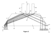
- Figure 1 is a schematic cross sectional view of an optical navigation device 1 comprising a laser diode 2, an optical waveguide layer 4 and an image sensor 6.
- the laser diode 2 and image sensor 6 are mounted on separate circuit boards 7a, 7b, while the optical waveguide layer 4 is suspended above the circuit boards 7a, 7b by a supportive housing 8. It will be understood that the laser 2 and image sensor 6 may alternatively be mounted on the same circuit board (see Figure 7 ).
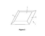
- the optical waveguide layer 4 comprises an upper, user input face 9 and a lower face 10 with a pair of angled side faces 12, 14 extending between them, the side faces 12, 14 converging towards each other as they extend from the lower face 10 to the upper face 9.
- a touch sensitive input pad 15 is formed at an intermediate region of the user input face 9 between the angled faces 12, 14.
- the input pad 15 has an exposed user (or 'mousing') surface 16 (which is exposed to the ambient environment) and a total internal reflection (TIR) surface 18 (which is internal to the waveguide layer 4) on the underside (that is, the reverse side) of the exposed user surface 16.
- the waveguide layer 4 typically has a refractive index in the range 1.5-2.0 and may be formed for example from polycarbonate (refractive index approximately 1.59).
- the image sensor 6 has an imaging surface 22 comprising an array of pixels.
- the array comprises a 20x20 array of 30 ⁇ m CMOS pixels.
- CMOS complementary metal-oxide-semiconductor
- the sensor further comprises a signal processor.
- the laser 2, image sensor 6 and waveguide layer 4 are together arranged such that, when radiation 24 is emitted by the laser 2, it enters the waveguide layer 4 and is directed onto the imaging surface 22 of the image sensor 6 via the TIR surface 18 by total internal reflection.
- the angled surfaces 12, 14 are also TIR surfaces.
- radiation is emitted by the laser 2 along a first principal optical axis 25a towards a first one of the angled faces 12 of the optical waveguide layer 4.
- the first angled face 12 then directs the radiation 24 towards the TIR surface 18 along a second principal optical axis 25b by total internal reflection.
- the radiation 24 is then totally internally reflected by the TIR surface 18 along a third principal optical axis 25c towards the second angled face 14.
- the second angled face 14 totally internally reflects the radiation 24 along a fourth principal optical axis 25d towards the imaging surface 22 of the image sensor 6. It will be understood that, in each case, the laser radiation is incident on the TIR surfaces at an angle greater than the critical angle for total internal reflection. It is also noted that the system of Figure 1 is typically afocal - that is, the laser radiation is not typically focussed onto the image sensor 6.
- the waveguide layer 4 is arranged such that the radiation reflected by the side face 14 is not totally internally reflected by the lower face 10 of the waveguide layer 4. Rather, the radiation passes through the lower face 10 onto the imaging surface 22, thus causing substantially all of (or only some of, but preferably at least the majority of) the pixels of the pixel array to be illuminated.
- the laser diode 2 and the image sensor 6 have principal optical axes 25a, 25d respectively which are substantially parallel to each other.
- the circuit boards 7a, 7b on which the laser 2 and image sensor 6 are mounted may be co-planar or alternatively they may be located on separate parallel planes.
- the position and surface area of the touch sensitive input pad 15 is defined by the area of the user input face 9 which is illuminated by the laser 2. This depends on the divergent angle of the laser beam (in this case approximately 10°), the angle at which the laser beam is incident on the first angled face 12 and the degree of incline of the first angled face 12 relative to the user input face 9. It will be understood that, in an alternative embodiment, the optical waveguide layer may be arranged such that the entire user input face 9 is illuminated by the laser radiation (and is thus touch sensitive).
- the geometry of the waveguide layer 4 (in particular the degree of incline of the angled faces 12, 14 relative to the principal optical axis 25a, 25c of the laser radiation incident thereon) may be such that the laser radiation is incident upon the angled faces 12, 14 at an angle less than the critical angle for total internal reflection.
- a reflective coating e.g. aluminium
- total internal reflection by the TIR surface 18 of the input pad 15 is possible because the laser radiation beam is incident on the TIR surface(s) at an angle greater than the critical angle for total internal reflection.
- a human digit such as a finger or a thumb (which has a larger refractive index than the ambient air) touches the exposed user surface 16
- the ridges 26-28 of the finger (or thumb) print frustrate the total internal reflection (F-TIR) at the TIR surface 18.
- the portion 24a of radiation 24 which is incident on the TIR surface 18 directly beneath where the digit contacts the exposed user surface 16 is no longer totally internally reflected and instead escapes from the waveguide layer 4. This occurs because the increased refractive index (compared to that of the ambient air) of the digit touching the exposed user surface 16 increases the critical angle for total internal reflection above the angle of incidence of the laser radiation beam.
- a portion (typically around 10%) of the escaped radiation 24a is scattered off the digit back into the waveguide layer 4 towards the second angled face 14 and onto the imaging surface 22.
- any radiation which does not undergo F-TIR is directed onto the imaging surface as before.
- less radiation is incident on the image sensor when a digit is in contact with the input pad 15, resulting in fewer of the pixels in the pixel array being illuminated. This causes an image pattern 30 to be formed on the imaging surface 22.
- FIG. 5 An exemplary image pattern is shown in Figure 5 .
- a 20x20 pixel array (which in total has a width of 0.608mm and a height of 0.608mm) is illuminated with a peak irradiance of 1.5W/cm 2 and a total power of 2.1mW.
- the frustrated total internal reflection (caused by the digit ridges touching the exposed user surface) at the TIR surface 18 results in the detection of an image pattern comprising a series of dark and illuminated regions 30a, 30b.
- the navigation device 1 is operated by sliding a digit 28 across the touch sensitive exposed user surface 16 and user input information is derived from changes in sequential image frames detected at the imaging surface.
- the position of F-TIR on the input pad 15 changes and the image pattern formed on the imaging surface 22 changes accordingly.
- the signal processor of the sensor processes successive image patterns to identify the point or points of contact of the digit on the exposed user surface 16 and to determine motion vectors and the rate of movement of one or more features from one frame to the next. The motion vectors and rate of movement can then be translated into an appropriate control action for a mobile communications device or mobile computer (for example).
- the device may work at a frame rate of 1 kHz to 10kHz in order to detect relative movement or movements of one or more features at the exposed user surface 16 of the input pad 15.
- the frame rate is set by the refresh rate of the sensor.
- the exposure may be achieved by a pulsating laser source or by sampling the sensor output at the required rate.
- the features detected by the sensor may be between around 0.5mm and 30 ⁇ m in size. The smaller features provide a greater ability to detect motion than the larger ones.
- the radiation beam emitted by the laser diode has low beam divergence (less than 10° typically), no collimation or imaging optics may be required.
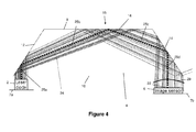
- the magnifying lens 29 is convex with respect to the incident direction of the laser radiation.
- Figures 6 to 8 show an alternative embodiment of the optical navigation device 1.
- the embodiment of Figures 6 to 8 is similar to that described in Figures 1 to 4 and identical features are given the same reference numerals.
- the laser 2 and image sensor 6 are mounted on a common circuit board 34 and housed within separate compartments 35, 36 respectively of the housing 8.
- a beam expanding hemispherical lens 37 (shown most clearly in Figure 8 ) is provided over the emitting surface of the laser 2 to increase the diameter of the radiation beam emitted by the laser 2.
- the lens 37 is typically mounted on an upper surface of the laser 2, as shown in Figure 8 .
- a collimating Fresnel lens 38 is provided over the beam expanding lens 37 to collimate the expanded laser radiation beam before it is totally internally reflected by the first angled internal surface 12 of the waveguide layer 4 towards the TIR surface 18.
- a vertical gap 'd' (most clearly illustrated in the side view of Figure 7 ) is provided between the beam expanding lens 37 and the collimating Fresnel lens 38 to allow the beam diameter to be expanded before it is collimated. This ensures that the laser radiation illuminates a sufficient amount of the TIR surface 18, which in turn makes a sufficient amount of the exposed user surface 16 touch sensitive.
- the collimating lens 38 increases the uniformity of illumination of the TIR surface 18. This improves the contrast between these parts of the image detected by the image sensor where FTIR has occurred and those parts of the image where FTIR has not occurred. This in turn improves the performance of the optical navigation device 1 as the signal processor can more accurately detect the location of FTIR in successive image frames.
- the thickness of the housing 8 does not need to be significantly increased to accommodate it.
- the collimating lens 38 may also eliminate any need for a magnifying lens 29 to be provided over the image sensor 6 (although it will be understood that neither a Fresnel lens nor a magnifying lens may be required).
- this design may allow the thickness of the housing 8 to be reduced
- the collimating lens 38 may be formed separately from the waveguide 4 and attached thereto with transparent adhesive.
- the collimating lens 38 may be integrally formed with the waveguide 4.
- the radiation beam emitted by the laser 2 when the radiation beam emitted by the laser 2 is incident on the TIR surface 18, it becomes “stretched” (i.e. it becomes oval rather than circular in cross section) compared to where it is incident on the first angled side face 12.
- this "stretching" is corrected by the second angled side face 14 (which preferably has the same angle of inclination with respect to the user input face 9 as the first angled face 12) before it is incident on the image sensor 6 (i.e. the beam has a circular cross section when it is incident on the image sensor 6).
- a correction lens 39 may be provided above the image sensor 6 to correct this magnification difference.
- the correction lens is typically cylindrical and may (or may not) be a Fresnel lens. As above, the Fresnel type lens is preferred as it is significantly thinner than more traditional lenses having the same aperture and focal length.
- the correction lens may be integrally formed with the waveguide layer 4 or, alternatively, formed separately from the waveguide layer 4 and attached thereto by transparent adhesive.
- a logo 40 which is provided on a centre portion of the lower face 10 of the waveguide layer 4 directly under the exposed user surface 16.
- the logo 40 is recessed into the lower face 10 of the waveguide layer 4 to a depth of approximately 30-50 ⁇ m.
- the logo 40 is formed by moulding the lower face 10 against a mould tool comprising a raised logo template formed on the mould tool by spark erosion. Spark erosion also causes a surface roughness or 'texture' to be applied to the raised logo template on the mould tool. This surface roughness (or 'texture') causes a similar texture to be applied to one or more recessed surfaces of the logo 40 during moulding.
- a visible light source 42 such as a light emitting diode (LED), is also provided on the circuit board 34 between the laser 2 and the image sensor 6.
- the LED 42 is arranged such that its principle optical emission axis is aligned with both the logo 40 and the exposed user surface 16. Light emitted by the LED 42 is thus directed towards the logo 40. Light incident on the textured part(s) of the logo 40 is scattered, while light which is incident on any non-textured parts of the logo or the surrounding (non-textured) region of the lower face 10 is transmitted through the waveguide 4 substantially un-attenuated.
- the logo 40 will thus appear to 'glow' to a user of the navigation device through the exposed user surface 16, and can therefore be used, for example, for advertising and/or aesthetic purposes.
- a selective wavelength optical filter may optionally be provided over the image sensor 6 (i.e. a filter which transmits the, typically infrared, laser radiation and blocks visible radiation).
- any other suitable object for example a glove or stylus
- a refractive index which is greater than 1, more preferably greater than 1.5, and most preferably greater than the refractive index of the waveguide layer 4 which is sufficiently large to increase the critical angle above the angle of incidence of the laser radiation beam on the TIR surface 18.
- the upper, input face 9 is shown as being substantially flat in Figures 1-4 and in Figure 6 , it is noted that, for ergonomic reasons, it may be preferable for the upper, input face to be curved so as to form a dome protruding from the top of the optical navigation device.
- Figure 9 shows an alternative embodiment of the optical navigation device 1 which in this case comprises an alternative waveguide layer 4a.
- the waveguide layer 4a is similar to the waveguide layer 4 of the optical navigation device 1 described above.
- the angled side faces 12a, 14a are substantially parallel to each other.
- the laser diode 2 is mounted on a plane which is perpendicular to the plane on which the image sensor 6 is mounted. It will be understood that, if the laser diode 2 and image sensor 6 are to be mounted on the same circuit board, it must be flexible to allow the laser 2 and sensor 6 to be mounted on perpendicular planes.
- radiation 24 is emitted by the laser 2 along a first principal optical axis 32a towards the first angled side face 12a.
- the first side face 12a is angled with respect to the principal optical axis 32a of the laser radiation such that, when the radiation enters the waveguide layer 4a (which has a larger refractive index than the air or vacuum between the laser diode 2 and the waveguide layer 4a), the radiation is refracted along a second principal optical axis 32b towards the TIR surface 18a.
- the radiation is then totally internally reflected by the TIR surface 18a along a third principal optical axis 32c towards the second angled face 14a.
- the second angled face 14a totally internally reflects the radiation 24 along a fourth principal optical axis 32d towards the imaging surface 22 of the image sensor 6.
- User input is provided to the optical navigation device 1a by frustrated total internal reflection as described above.
- a reflective aluminium coating may be applied to the side face 14a to improve its reflectivity. If an angle greater than the critical angle is achieved, preferably no aluminium coating is applied to the side face 14a as its reflectivity is greater in the absence of such a coating.
- the laser diode 2 and the image sensor 6 are mounted on perpendicular planes, they have principal optical axes 32a, 32d which are substantially perpendicular to each other. However, it will be understood that any angle may be formed between the principal optical axes 32a, 32d as long as the laser 2, waveguide layer 4 and image sensor 6 are together arranged to direct radiation emitted by the laser onto the imaging surface 22 at least partly by total internal reflection of the laser radiation 24 by the TIR surface 18a.
- the laser diode will be a VCSEL which preferably emits invisible infrared (or ultraviolet) radiation so as not to distract the user.
- the laser may emit visible light, in which case a small amount of visible light will leak, when the device is operated, in the vicinity of the user's digit.
- optical navigation device Because of the small thickness of device which can be achieved with the optical navigation device, it is particularly useful in hand-held mobile apparatus such as phones, PDAs and personal music players.
- the optical navigation device is also useful in computers (especially laptops and notebooks), remote controls, game controllers, and mice.
- Figure 10 illustrates an electronic apparatus 50 comprising an optical navigation device 1 according to any of the above described embodiments of the disclosure.
- the electronic apparatus 50 may be a mobile communications device such as a mobile phone or a personal data assistant.
Landscapes
- Engineering & Computer Science (AREA)
- General Engineering & Computer Science (AREA)
- Theoretical Computer Science (AREA)
- Physics & Mathematics (AREA)
- General Physics & Mathematics (AREA)
- Human Computer Interaction (AREA)
- Computer Hardware Design (AREA)
- Multimedia (AREA)
- Optics & Photonics (AREA)
- Studio Devices (AREA)
- Image Input (AREA)
- Optical Radar Systems And Details Thereof (AREA)
- Photo Coupler, Interrupter, Optical-To-Optical Conversion Devices (AREA)
Abstract
Description
- This invention relates to an optical navigation device suitable for mobile electronic devices such as mobile communication devices, personal data assistants, personal music players and the like which is operated by moving an object on its surface, sometimes referred to as a finger mouse.
- Current mobile or computer devices use a variety of different navigation mechanisms including trackball devices, multi-click joysticks and capacitance based touch pads. However, there are problems associated with each of these. Trackballs and joysticks can be unreliable and relatively expensive to implement. In addition, capacitance based touch pads do not operate satisfactorily if the finger is covered, for example by a glove, and their size can be large in relation to devices such as mobile phones and PDAs.
- Optical navigation devices are also known which operate on the same principles as optical mice by comparing successive frames of an area image. However, conventional devices use LED light sources which require collimation and imaging optics which contribute to the thickness of the devices.
- There is therefore a need to provide an optical navigation device which has a reduced thickness compared to existing devices and which operates in a safe manner. In addition, it is desirable that such a device can be manufactured in a simple manner and with a low part count.
- A first aspect of the present disclosure comprises an optical navigation device comprising: an image sensor with an imaging surface; a laser; and an optical waveguide layer having an exposed user surface and a total internal reflection (TIR) surface on the underside of the exposed user surface, wherein the waveguide layer, laser and image sensor are together arranged to direct radiation emitted by the laser onto the imaging surface at least partly by total internal reflection by the TIR surface.
- The laser radiation is contained within the optical navigation device (primarily within the waveguide layer) unless an object (such as a human digit) comes into contact with the exposed user surface to frustrate the total internal reflection at the TIR surface. In this case, some laser radiation will escape from the device but will be absorbed by the object contacting the exposed user surface (with some of the radiation subsequently being scattered back into the waveguide layer). Therefore, whether an object is in contact with the exposed user surface or not, there is no risk of radiation escaping from the device in such a way that it would cause damage to a user's eyes. The device is thus intrinsically safe, in contrast to an optical navigation device which continuously emits coherent laser radiation (potentially in the direction of the user's eyes).
- In one embodiment, the optical waveguide layer further comprises a first internal surface adapted to reflect radiation emitted by the laser towards the TIR surface. Additionally or alternatively, the optical waveguide layer preferably further comprises a second internal surface adapted to reflect radiation reflected by the TIR surface towards the imaging surface. In both cases, it is preferable that the internal surfaces are adapted to totally internally reflect the laser radiation. However, where this is not possible (for example due to the geometry of the waveguide layer), a coating (e.g. aluminium) may be applied to the first and/or second internal surfaces to make them more reflective. Typically, the first and second internal surfaces are angled with respect to the principal optical axis of the radiation incident thereon.
- As an alternative to providing a first internal surface adapted to reflect radiation emitted by the laser towards the TIR surface, the waveguide layer may be adapted to refract radiation emitted by the laser towards the TIR surface.
- In one embodiment, a first lens is provided over the laser, the first lens being configured to substantially collimate radiation emitted by the laser. By collimating the laser radiation, a more uniform illumination of the TIR surface by the laser radiation is achieved. This results in better performance of the navigation device.
- Additionally or alternatively, a second lens may be provided between the first lens and the laser, the second lens being configured to expand the diameter of a radiation beam emitted by the laser. The second lens may be mounted on an upper surface of the laser.
- Where both the first and second lenses are provided, a gap is preferably provided between the first and second lenses. This provides space for the radiation beam to expand after passing through the second lens before it is collimated by the first lens.
- The second lens is preferably positioned directly under the first lens (with or without a gap between them). In addition, the principle optical axes of the first and second lenses are preferably parallel. In one embodiment, the principle optical axes of the first and second lenses are co-linear.
- Preferably, the principle optical axes of the first and/or second lenses are substantially parallel to the principle optical axis of the radiation beam em itted by the laser.
- The first lens may be formed separately from the waveguide layer, but more preferably, the first lens is integrally formed with the waveguide layer to minimise the thickness of the navigation device.
- Preferably, the first lens is a Fresnel lens. Fresnel lenses are typically thinner than more traditional lenses having the same aperture and focal length. Therefore, by employing a Fresnel lens instead of a more traditional lens, the thickness of the device can be minimised, while retaining the benefits of collimation (see above).
- Typically, the laser and image sensor of the device are housed within separate compartments of a single sensor package. This prevents any unwanted internal propagation of radiation from the laser to the image sensor within the sensor housing, without it first being reflected via the TIR surface.
- A laser is employed rather than, for example, a light emitting diode (LED) as the radiation emitted is more coherent - that is, although the photons emitted by the laser may be diverging, they are emitted in substantially the same direction. Therefore, any modification of the beam by frustrated TIR can be observed at any point along that beam without the need for imaging optics. This lack of imaging optics also means that the assembly process of the optical navigation device does not need to be as accurately toleranced - that is, assembly is made easier.
- Any suitable laser may be used. For example, the laser may be a distributed feedback (DFB) laser. However, these lasers tend to be provided in relatively large modules. Therefore, more preferably, the laser is a vertical cavity surface emitting laser (VCSEL), which tend to be provided in smaller chip-sized packages.
- The laser and image sensor may have principal optical axes which are parallel to each other. Alternatively, the laser and image sensor may have principal optical axes which are not parallel to each other.
- Preferably the waveguide layer is monolithic. The waveguide layer is typically provided over the laser and the imaging sensor.
- In one embodiment, the optical navigation device further comprises a magnifying lens adjacent the imaging surface. This helps to ensure that the entire imaging surface is illuminated so as to form a more reliable imaging pattern. Typically, the magnifying lens is positioned over the imaging surface.
- Additionally or alternatively, in a preferred embodiment, a correction lens is positioned over the imaging surface for correcting a magnification effect in the laser radiation reflected by the TIR surface. Typically, when frustrated total internal reflection occurs at the TIR surface, a magnification difference is observed at the imaging surface between the X and Y axes. This may be corrected by the correction lens. In one embodiment, the correction lens may be cylindrical. Additionally, or alternatively, the correction lens may be a Fresnel lens.
- The greater the refractive index of the waveguide layer, the lower the critical angle for TIR (i.e. the angle between the laser radiation beam incident on the TIR surface and the normal to the TIR surface). Therefore, the greater the refractive index of the waveguide layer, the narrower (with respect to the incident direction of the laser radiation on the TIR surface) the waveguide layer can be. As miniaturisation is an important concern for optical navigation devices of this type, it is thus preferable that the refractive index of the optical waveguide layer is as high as possible (typically greater than 1, preferably greater than 1.5, more preferably greater than 2). However, due to the increased cost of suitable materials with higher refractive indices, the optical waveguide layer typically has a refractive index of between 1 and 2.
- A second aspect of the present disclosure provides a method of operating an optical navigation device comprising: an image sensor with an imaging surface; a laser; and an optical waveguide layer having an exposed user surface and a total internal reflection (TIR) surface on the underside of the exposed user surface, the method comprising: totally internally reflecting radiation emitted by the laser using the TIR surface; illuminating at least part of the imaging surface with the reflected radiation; bringing an object into contact with the exposed user surface to frustrate total internal reflection of at least a portion of the laser radiation at the TIR surface; and deriving user input information from changes in sequential image frames detected at the imaging surface.
- Preferably, the method further comprises moving the object across the exposed user surface. The object is preferably a human digit or a stylus.
- In one embodiment, the method according to the second aspect of the disclosure further comprises collimating radiation emitted by the laser. Typically, the radiation is collimated by a Fresnel lens.
- Additionally or alternatively, the method according to the second aspect of the disclosure may further comprise expanding the diameter of a radiation beam emitted by the laser before collimating the radiation beam.
- A third aspect of the disclosure provides electronic apparatus comprising an optical navigation device having an image sensor with an imaging surface; a laser; and an optical waveguide layer having an exposed user surface and a total internal reflection (TIR) surface on the underside of the exposed user surface, wherein the waveguide layer, laser and image sensor are together arranged to direct radiation emitted by the laser onto the imaging surface at least partly by total internal reflection by the TIR surface.
- A fourth aspect of the disclosure provides a mobile communications device comprising an optical navigation device having an image sensor with an imaging surface; a laser; and an optical waveguide layer having an exposed user surface and a total internal reflection (TIR) surface on the underside of the exposed user surface, wherein the waveguide layer, laser and image sensor are together arranged to direct radiation emitted by the laser onto the imaging surface at least partly by total internal reflection by the TIR surface.
- An embodiment of the invention will now be described, by way of example only, with reference to the drawings, in which:
-
Figure 1 is a schematic cross sectional view of an optical navigation device according to the disclosure; -
Figure 2 is a schematic perspective view of the waveguide layer of the optical navigation device ofFig. 1 ; -
Figure 3 is similar toFig.1 but further includes an object touching an exposed user surface of the device; -
Figure 4 is similar toFig. 1 but further includes a magnifying lens adjacent (in this case positioned over) the image sensor of the device; -
Figure 5 shows an image pattern produced by the image sensor when an object touches the exposed user surface when the device is in use; -
Figure 6 is a perspective section view of an alternative optical navigation device comprising a Fresnel collimating lens; -
Figure 7 is a side view of the device ofFig. 6 , which in this case also comprises a correction lens over the image sensor; -
Figure 8 is an exploded view of the device ofFig. 6 ; -
Figure 9 shows another alternative embodiment of the optical navigation device ofFigures 1 and2 wherein the laser and image sensor have principal optical axes which are oriented at approximately 90° to each other; and -
Figure 10 shows an electronic apparatus comprising an optical navigation device according to the present disclosure. -
Figure 1 is a schematic cross sectional view of anoptical navigation device 1 comprising alaser diode 2, anoptical waveguide layer 4 and animage sensor 6. Thelaser diode 2 andimage sensor 6 are mounted onseparate circuit boards optical waveguide layer 4 is suspended above thecircuit boards supportive housing 8. It will be understood that thelaser 2 andimage sensor 6 may alternatively be mounted on the same circuit board (seeFigure 7 ). As shown inFigures 1 and2 , theoptical waveguide layer 4 comprises an upper,user input face 9 and alower face 10 with a pair of angled side faces 12, 14 extending between them, the side faces 12, 14 converging towards each other as they extend from thelower face 10 to theupper face 9. A touchsensitive input pad 15 is formed at an intermediate region of theuser input face 9 between the angled faces 12, 14. Theinput pad 15 has an exposed user (or 'mousing') surface 16 (which is exposed to the ambient environment) and a total internal reflection (TIR) surface 18 (which is internal to the waveguide layer 4) on the underside (that is, the reverse side) of the exposeduser surface 16. Thewaveguide layer 4 typically has a refractive index in the range 1.5-2.0 and may be formed for example from polycarbonate (refractive index approximately 1.59). - The
image sensor 6 has animaging surface 22 comprising an array of pixels. In the present embodiment, the array comprises a 20x20 array of 30µm CMOS pixels. However, it will be understood that other array sizes/architectures may be employed and that any suitable alternative technology to CMOS (such as CCD) may be used in the pixels. The sensor further comprises a signal processor. - The
laser 2,image sensor 6 andwaveguide layer 4 are together arranged such that, whenradiation 24 is emitted by thelaser 2, it enters thewaveguide layer 4 and is directed onto theimaging surface 22 of theimage sensor 6 via theTIR surface 18 by total internal reflection. In one embodiment, theangled surfaces laser 2 along a first principaloptical axis 25a towards a first one of the angled faces 12 of theoptical waveguide layer 4. The firstangled face 12 then directs theradiation 24 towards theTIR surface 18 along a second principaloptical axis 25b by total internal reflection. Theradiation 24 is then totally internally reflected by theTIR surface 18 along a third principaloptical axis 25c towards the secondangled face 14. Finally, the secondangled face 14 totally internally reflects theradiation 24 along a fourth principaloptical axis 25d towards theimaging surface 22 of theimage sensor 6. It will be understood that, in each case, the laser radiation is incident on the TIR surfaces at an angle greater than the critical angle for total internal reflection. It is also noted that the system ofFigure 1 is typically afocal - that is, the laser radiation is not typically focussed onto theimage sensor 6. - As shown in
Figure 1 , thewaveguide layer 4 is arranged such that the radiation reflected by theside face 14 is not totally internally reflected by thelower face 10 of thewaveguide layer 4. Rather, the radiation passes through thelower face 10 onto theimaging surface 22, thus causing substantially all of (or only some of, but preferably at least the majority of) the pixels of the pixel array to be illuminated. - In the embodiment shown in
Figure 1 , thelaser diode 2 and theimage sensor 6 have principaloptical axes circuit boards laser 2 andimage sensor 6 are mounted may be co-planar or alternatively they may be located on separate parallel planes. - As explained below, the position and surface area of the touch
sensitive input pad 15 is defined by the area of theuser input face 9 which is illuminated by thelaser 2. This depends on the divergent angle of the laser beam (in this case approximately 10°), the angle at which the laser beam is incident on the firstangled face 12 and the degree of incline of the firstangled face 12 relative to theuser input face 9. It will be understood that, in an alternative embodiment, the optical waveguide layer may be arranged such that the entireuser input face 9 is illuminated by the laser radiation (and is thus touch sensitive). - In some cases, the geometry of the waveguide layer 4 (in particular the degree of incline of the angled faces 12, 14 relative to the principal
optical axis input pad 15 and theimage sensor 6 respectively. - As mentioned above, total internal reflection by the
TIR surface 18 of the input pad 15 (and by the angled faces 12, 14) is possible because the laser radiation beam is incident on the TIR surface(s) at an angle greater than the critical angle for total internal reflection. The critical angle (θc=sin-1(n2/n1)) is dependent on the refractive index (n1) of thewaveguide layer 4 and the refractive index (n2) of the ambient air on the exposeduser surface 16. However, as shown inFigure 3 , when a human digit such as a finger or a thumb (which has a larger refractive index than the ambient air) touches the exposeduser surface 16, the ridges 26-28 of the finger (or thumb) print frustrate the total internal reflection (F-TIR) at theTIR surface 18. That is, as shown inFigure 3 , theportion 24a ofradiation 24 which is incident on theTIR surface 18 directly beneath where the digit contacts the exposeduser surface 16 is no longer totally internally reflected and instead escapes from thewaveguide layer 4. This occurs because the increased refractive index (compared to that of the ambient air) of the digit touching the exposeduser surface 16 increases the critical angle for total internal reflection above the angle of incidence of the laser radiation beam. - Although not shown in
Figure 3 , a portion (typically around 10%) of the escapedradiation 24a is scattered off the digit back into thewaveguide layer 4 towards the secondangled face 14 and onto theimaging surface 22. In addition, any radiation which does not undergo F-TIR is directed onto the imaging surface as before. However, less radiation is incident on the image sensor when a digit is in contact with theinput pad 15, resulting in fewer of the pixels in the pixel array being illuminated. This causes animage pattern 30 to be formed on theimaging surface 22. - An exemplary image pattern is shown in
Figure 5 . In this case, a 20x20 pixel array (which in total has a width of 0.608mm and a height of 0.608mm) is illuminated with a peak irradiance of 1.5W/cm2 and a total power of 2.1mW. The frustrated total internal reflection (caused by the digit ridges touching the exposed user surface) at theTIR surface 18 results in the detection of an image pattern comprising a series of dark andilluminated regions - The
navigation device 1 is operated by sliding adigit 28 across the touch sensitive exposeduser surface 16 and user input information is derived from changes in sequential image frames detected at the imaging surface. In particular, as thedigit 28 moves across the surface, the position of F-TIR on theinput pad 15 changes and the image pattern formed on theimaging surface 22 changes accordingly. The signal processor of the sensor processes successive image patterns to identify the point or points of contact of the digit on the exposeduser surface 16 and to determine motion vectors and the rate of movement of one or more features from one frame to the next. The motion vectors and rate of movement can then be translated into an appropriate control action for a mobile communications device or mobile computer (for example). The device may work at a frame rate of 1 kHz to 10kHz in order to detect relative movement or movements of one or more features at the exposeduser surface 16 of theinput pad 15. The frame rate is set by the refresh rate of the sensor. The exposure may be achieved by a pulsating laser source or by sampling the sensor output at the required rate. The features detected by the sensor may be between around 0.5mm and 30µm in size. The smaller features provide a greater ability to detect motion than the larger ones. - It may be possible to calibrate the sensor by determining the sensor illumination when the
laser diode 2 is turned off and comparing this with the sensor illumination when thelaser diode 2 is on. This calibration may occur at the start of each use of the optical navigation device or on a frame to frame basis. - As the radiation beam emitted by the laser diode has low beam divergence (less than 10° typically), no collimation or imaging optics may be required. This allows the navigation device to be much thinner than conventional devices which use optics such as lenses and collimators. It also reduces part count and makes manufacture easier. However, depending on the geometry of the device, it may be necessary/beneficial to include a magnifying lens 29 (see
Figure 4 ) between thewaveguide layer 4 and theimaging surface 22 to ensure that the entire imaging surface is illuminated so as to form a reliable imaging pattern. In the embodiment shown inFigure 4 , the magnifyinglens 29 is convex with respect to the incident direction of the laser radiation. -
Figures 6 to 8 show an alternative embodiment of theoptical navigation device 1. The embodiment ofFigures 6 to 8 is similar to that described inFigures 1 to 4 and identical features are given the same reference numerals. In this case, thelaser 2 andimage sensor 6 are mounted on acommon circuit board 34 and housed withinseparate compartments housing 8. A beam expanding hemispherical lens 37 (shown most clearly inFigure 8 ) is provided over the emitting surface of thelaser 2 to increase the diameter of the radiation beam emitted by thelaser 2. Thelens 37 is typically mounted on an upper surface of thelaser 2, as shown inFigure 8 . Acollimating Fresnel lens 38 is provided over thebeam expanding lens 37 to collimate the expanded laser radiation beam before it is totally internally reflected by the first angledinternal surface 12 of thewaveguide layer 4 towards theTIR surface 18. A vertical gap 'd' (most clearly illustrated in the side view ofFigure 7 ) is provided between thebeam expanding lens 37 and thecollimating Fresnel lens 38 to allow the beam diameter to be expanded before it is collimated. This ensures that the laser radiation illuminates a sufficient amount of theTIR surface 18, which in turn makes a sufficient amount of the exposeduser surface 16 touch sensitive. - The collimating
lens 38 increases the uniformity of illumination of theTIR surface 18. This improves the contrast between these parts of the image detected by the image sensor where FTIR has occurred and those parts of the image where FTIR has not occurred. This in turn improves the performance of theoptical navigation device 1 as the signal processor can more accurately detect the location of FTIR in successive image frames. - It will be understood that, as the
Fresnel lens 38 is significantly thinner than more traditional lenses having the same aperture and focal length, the thickness of thehousing 8 does not need to be significantly increased to accommodate it. Furthermore, the collimatinglens 38 may also eliminate any need for a magnifyinglens 29 to be provided over the image sensor 6 (although it will be understood that neither a Fresnel lens nor a magnifying lens may be required). As theFresnel collimating lens 38 is typically thinner than atraditional magnifying lens 29, this design may allow the thickness of thehousing 8 to be reduced - Optionally, the collimating
lens 38 may be formed separately from thewaveguide 4 and attached thereto with transparent adhesive. Alternatively, the collimatinglens 38 may be integrally formed with thewaveguide 4. - It will be understood that, when the radiation beam emitted by the
laser 2 is incident on theTIR surface 18, it becomes "stretched" (i.e. it becomes oval rather than circular in cross section) compared to where it is incident on the firstangled side face 12. When there is no frustrated TIR, this "stretching" is corrected by the second angled side face 14 (which preferably has the same angle of inclination with respect to theuser input face 9 as the first angled face 12) before it is incident on the image sensor 6 (i.e. the beam has a circular cross section when it is incident on the image sensor 6). However, when frustrated total internal reflection occurs at the exposed user surface 16 (when the beam is stretched), not all of the beam "stretching" is corrected and a magnification difference occurs between the X and Y directions of the modified laser image incident on theimage sensor 6. This is because the laser radiation beam is modified in its stretched state. Optionally, acorrection lens 39 may be provided above theimage sensor 6 to correct this magnification difference. This is shown inFigure 7 . The correction lens is typically cylindrical and may (or may not) be a Fresnel lens. As above, the Fresnel type lens is preferred as it is significantly thinner than more traditional lenses having the same aperture and focal length. In addition, the correction lens may be integrally formed with thewaveguide layer 4 or, alternatively, formed separately from thewaveguide layer 4 and attached thereto by transparent adhesive. - Also shown in
Figures 6 and8 is alogo 40 which is provided on a centre portion of thelower face 10 of thewaveguide layer 4 directly under the exposeduser surface 16. Thelogo 40 is recessed into thelower face 10 of thewaveguide layer 4 to a depth of approximately 30-50µm. Typically, thelogo 40 is formed by moulding thelower face 10 against a mould tool comprising a raised logo template formed on the mould tool by spark erosion. Spark erosion also causes a surface roughness or 'texture' to be applied to the raised logo template on the mould tool. This surface roughness (or 'texture') causes a similar texture to be applied to one or more recessed surfaces of thelogo 40 during moulding. A visible light source 42 (seeFigure 6 ), such as a light emitting diode (LED), is also provided on thecircuit board 34 between thelaser 2 and theimage sensor 6. TheLED 42 is arranged such that its principle optical emission axis is aligned with both thelogo 40 and the exposeduser surface 16. Light emitted by theLED 42 is thus directed towards thelogo 40. Light incident on the textured part(s) of thelogo 40 is scattered, while light which is incident on any non-textured parts of the logo or the surrounding (non-textured) region of thelower face 10 is transmitted through thewaveguide 4 substantially un-attenuated. Thelogo 40 will thus appear to 'glow' to a user of the navigation device through the exposeduser surface 16, and can therefore be used, for example, for advertising and/or aesthetic purposes. - It will be understood that some visible light emitted by the
LED 42 may be reflected by TIR surface 18 (or by the angled faces 12, 14) rather than exiting the device through the exposeduser surface 16. However, only a minimal amount of visible light is typically reflected back onto theimage sensor 6. This is explained as follows. As the radiation emitted by thelaser 2 is collimated by the collimatinglens 38, the laser radiation travels along a well defined optical path within thehousing 8, and is incident on theimage sensor 6 at a specific angle of incidence. The imagesensor housing compartment 36 is arranged to restrict the viewing cone of theimage sensor 6 to a narrow range of viewing angles around this specific angle of incidence. This narrow viewing cone minimises the amount of unwanted reflected LED light captured by theimage sensor 6, without reducing the amount of laser radiation captured. Therefore, the laser image detected by theimage sensor 6 is not significantly distorted (typically) by the reflected LED light. - To provide added protection against distortion of the laser image by reflected LED light (or indeed by ambient radiation incident on the exposed user surface 16), a selective wavelength optical filter may optionally be provided over the image sensor 6 (i.e. a filter which transmits the, typically infrared, laser radiation and blocks visible radiation).
- It is noted that, instead of a user's digit, any other suitable object (for example a glove or stylus) may be used to provide the input by causing F-TIR. Such an object should have a refractive index (which is greater than 1, more preferably greater than 1.5, and most preferably greater than the refractive index of the waveguide layer 4) which is sufficiently large to increase the critical angle above the angle of incidence of the laser radiation beam on the
TIR surface 18. - Although the upper,
input face 9 is shown as being substantially flat inFigures 1-4 and inFigure 6 , it is noted that, for ergonomic reasons, it may be preferable for the upper, input face to be curved so as to form a dome protruding from the top of the optical navigation device. -
Figure 9 shows an alternative embodiment of theoptical navigation device 1 which in this case comprises analternative waveguide layer 4a. Thewaveguide layer 4a is similar to thewaveguide layer 4 of theoptical navigation device 1 described above. However, in this case, the angled side faces 12a, 14a are substantially parallel to each other. In addition, thelaser diode 2 is mounted on a plane which is perpendicular to the plane on which theimage sensor 6 is mounted. It will be understood that, if thelaser diode 2 andimage sensor 6 are to be mounted on the same circuit board, it must be flexible to allow thelaser 2 andsensor 6 to be mounted on perpendicular planes. - In the embodiment shown in
Figure 9 ,radiation 24 is emitted by thelaser 2 along a first principaloptical axis 32a towards the firstangled side face 12a. Thefirst side face 12a is angled with respect to the principaloptical axis 32a of the laser radiation such that, when the radiation enters thewaveguide layer 4a (which has a larger refractive index than the air or vacuum between thelaser diode 2 and thewaveguide layer 4a), the radiation is refracted along a second principaloptical axis 32b towards the TIR surface 18a. The radiation is then totally internally reflected by the TIR surface 18a along a third principaloptical axis 32c towards the secondangled face 14a. Finally, the secondangled face 14a totally internally reflects theradiation 24 along a fourth principaloptical axis 32d towards theimaging surface 22 of theimage sensor 6. User input is provided to the optical navigation device 1a by frustrated total internal reflection as described above. It will be understood that, as above, where it is not possible to achieve an angle greater than the critical angle, a reflective aluminium coating may be applied to theside face 14a to improve its reflectivity. If an angle greater than the critical angle is achieved, preferably no aluminium coating is applied to theside face 14a as its reflectivity is greater in the absence of such a coating. - As the
laser diode 2 and theimage sensor 6 are mounted on perpendicular planes, they have principaloptical axes optical axes laser 2,waveguide layer 4 andimage sensor 6 are together arranged to direct radiation emitted by the laser onto theimaging surface 22 at least partly by total internal reflection of thelaser radiation 24 by the TIR surface 18a. - Typically (but not exclusively), in each of the embodiments described above, the laser diode will be a VCSEL which preferably emits invisible infrared (or ultraviolet) radiation so as not to distract the user. Alternatively, the laser may emit visible light, in which case a small amount of visible light will leak, when the device is operated, in the vicinity of the user's digit.
- Because of the small thickness of device which can be achieved with the optical navigation device, it is particularly useful in hand-held mobile apparatus such as phones, PDAs and personal music players. The optical navigation device is also useful in computers (especially laptops and notebooks), remote controls, game controllers, and mice.
-
Figure 10 illustrates anelectronic apparatus 50 comprising anoptical navigation device 1 according to any of the above described embodiments of the disclosure. In one embodiment, theelectronic apparatus 50 may be a mobile communications device such as a mobile phone or a personal data assistant. - While this detailed description has set forth some embodiments of the present invention, the appended claims cover other embodiments of the present invention which may differ from the described embodiments according to various modifications and improvements.
Claims (15)
- An optical navigation device comprising: an image sensor with an imaging surface; a laser; and an optical waveguide layer having an exposed user surface and a total internal reflection (TIR) surface on the underside of the exposed user surface, wherein the waveguide layer, laser and image sensor are together arranged to direct radiation emitted by the laser onto the imaging surface at least partly by total internal reflection by the TIR surface.
- The optical navigation device of claim 1 wherein the optical waveguide layer further comprises a first internal surface adapted to reflect radiation emitted by the laser towards the TIR surface.
- The optical navigation device of claim 1 or 2 wherein the optical waveguide layer further comprises a second internal surface adapted to reflect radiation reflected by the TIR surface towards the imaging surface.
- The optical navigation device of claim 2 or 3 wherein the first and/or second internal surfaces are adapted to totally internally reflect the laser radiation.
- The optical navigation device of any preceding claim further comprising a first lens positioned over the laser, the first lens being configured to substantially collimate radiation emitted by the laser.
- The optical navigation device of claim 5 further comprising a second lens positioned between the first lens and the laser, the second lens being configured to expand the diameter of a radiation beam em itted by the laser.
- The optical navigation device of claim 6 further comprising a gap between the first and second lenses.
- The optical navigation device of any of claims 5 to 7 wherein the first lens is integrally formed with the waveguide layer.
- The optical navigation device of any of claims 5 to 8 wherein the first lens is a Fresnel lens.
- The optical navigation device of any preceding claim further comprising a correction lens positioned over the imaging surface for correcting a magnification effect in the laser radiation reflected by the TIR surface.
- The optical navigation device of claim 10 wherein the correction lens is cylindrical.
- The optical navigation device of claim 10 or 11 wherein the correction lens is a Fresnel lens.
- A method of operating an optical navigation device comprising: an image sensor with an imaging surface; a laser; and an optical waveguide layer having an exposed user surface and a total internal reflection (TIR) surface on the underside of the exposed user surface, the method comprising: totally internally reflecting radiation emitted by the laser using the TIR surface; illuminating at least part of the imaging surface with the reflected radiation; bringing an object into contact with the exposed user surface to frustrate total internal reflection of at least a portion of the laser radiation at the TIR surface; and deriving user input information from changes in sequential image frames detected at the imaging surface.
- Electronic apparatus comprising an optical navigation device having an image sensor with an imaging surface; a laser; and an optical waveguide layer having an exposed user surface and a total internal reflection (TIR) surface on the underside of the exposed user surface, wherein the waveguide layer, laser and image sensor are together arranged to direct radiation emitted by the laser onto the imaging surface at least partly by total internal reflection by the TIR surface.
- A mobile communications device comprising an optical navigation device having an image sensor with an imaging surface; a laser; and an optical waveguide layer having an exposed user surface and a total internal reflection (TIR) surface on the underside of the exposed user surface, wherein the waveguide layer, laser and image sensor are together arranged to direct radiation emitted by the laser onto the imaging surface at least partly by total internal reflection by the TIR surface.
Applications Claiming Priority (2)
| Application Number | Priority Date | Filing Date | Title |
|---|---|---|---|
| GBGB1014053.1A GB201014053D0 (en) | 2010-08-23 | 2010-08-23 | Optical navigation device |
| GBGB1021638.0A GB201021638D0 (en) | 2010-08-23 | 2010-12-21 | Optical navigation device |
Publications (2)
| Publication Number | Publication Date |
|---|---|
| EP2423793A2 true EP2423793A2 (en) | 2012-02-29 |
| EP2423793A3 EP2423793A3 (en) | 2014-08-13 |
Family
ID=42984499
Family Applications (1)
| Application Number | Title | Priority Date | Filing Date |
|---|---|---|---|
| EP11178528.3A Withdrawn EP2423793A3 (en) | 2010-08-23 | 2011-08-23 | Optical navigation device |
Country Status (4)
| Country | Link |
|---|---|
| US (1) | US9170684B2 (en) |
| EP (1) | EP2423793A3 (en) |
| CN (1) | CN102375621B (en) |
| GB (2) | GB201014053D0 (en) |
Cited By (1)
| Publication number | Priority date | Publication date | Assignee | Title |
|---|---|---|---|---|
| GB2497572A (en) * | 2011-12-15 | 2013-06-19 | St Microelectronics Ltd | Function performance in response to pattern recognition on an optical navigation device such as a finger mouse |
Families Citing this family (5)
| Publication number | Priority date | Publication date | Assignee | Title |
|---|---|---|---|---|
| US20150168606A1 (en) * | 2013-12-16 | 2015-06-18 | GE Lighting Solutions, LLC | Micro-lens base resin for led lightguide/waveguide applications |
| CN104793814A (en) * | 2015-05-12 | 2015-07-22 | 京东方科技集团股份有限公司 | Optical touch control device and touch control display device |
| TWI608733B (en) * | 2016-05-10 | 2017-12-11 | Infilm Optoelectronic Inc | Thin plate imaging device |
| US11178392B2 (en) * | 2018-09-12 | 2021-11-16 | Apple Inc. | Integrated optical emitters and applications thereof |
| US11886649B2 (en) * | 2021-11-25 | 2024-01-30 | Pixart Imaging Inc. | Optical navigation device |
Family Cites Families (26)
| Publication number | Priority date | Publication date | Assignee | Title |
|---|---|---|---|---|
| DE3856537T2 (en) * | 1987-11-16 | 2003-04-03 | Canon K.K., Tokio/Tokyo | The image recording device |
| DE69124822T2 (en) * | 1990-04-27 | 1997-10-09 | Omron Tateisi Electronics Co | Semiconductor light-emitting device with Fresnel lens |
| EP1073005A1 (en) | 1999-07-28 | 2001-01-31 | Siemens Aktiengesellschaft | User interface with optical sensor |
| EP1437677A1 (en) * | 2002-12-30 | 2004-07-14 | Nokia Corporation | Optical user interface for controlling portable electric device |
| JP3741108B2 (en) * | 2003-03-18 | 2006-02-01 | ソニー株式会社 | Laser light emitting module |
| US7274808B2 (en) | 2003-04-18 | 2007-09-25 | Avago Technologies Ecbu Ip (Singapore)Pte Ltd | Imaging system and apparatus for combining finger recognition and finger navigation |
| WO2004102523A1 (en) * | 2003-05-19 | 2004-11-25 | Itzhak Baruch | Optical coordinate input device comprising few elements |
| US8599140B2 (en) | 2004-11-17 | 2013-12-03 | International Business Machines Corporation | Providing a frustrated total internal reflection touch interface |
| US7232240B2 (en) | 2005-05-06 | 2007-06-19 | Northrop Grumann Corporation | Extended source laser illuminator |
| US7719517B2 (en) * | 2005-06-21 | 2010-05-18 | Microsoft Corporation | Input device for a computer system |
| US7737959B2 (en) * | 2005-09-08 | 2010-06-15 | Avago Technologies Ecbu Ip (Singapore) Pte. Ltd. | Position detection system using laser speckle |
| CN101000408A (en) * | 2006-01-10 | 2007-07-18 | 乐金电子(南京)等离子有限公司 | Total internal reflection prism |
| US8441467B2 (en) * | 2006-08-03 | 2013-05-14 | Perceptive Pixel Inc. | Multi-touch sensing display through frustrated total internal reflection |
| AR064377A1 (en) * | 2007-12-17 | 2009-04-01 | Rovere Victor Manuel Suarez | DEVICE FOR SENSING MULTIPLE CONTACT AREAS AGAINST OBJECTS SIMULTANEOUSLY |
| CN101488059B (en) * | 2008-01-18 | 2010-09-29 | 世纪民生科技股份有限公司 | Optical navigation sensor and optical navigation device thereof |
| KR20090105154A (en) | 2008-04-01 | 2009-10-07 | 크루셜텍 (주) | Click Recognition Method Using Optical Pointing Device and Optical Pointing Device |
| TW200945123A (en) | 2008-04-25 | 2009-11-01 | Ind Tech Res Inst | A multi-touch position tracking apparatus and interactive system and image processing method there of |
| US8237684B2 (en) | 2008-09-26 | 2012-08-07 | Avago Technologies Ecbu Ip (Singapore) Pte. Ltd. | User input device with planar light guide illumination plate |
| US20100079409A1 (en) | 2008-09-29 | 2010-04-01 | Smart Technologies Ulc | Touch panel for an interactive input system, and interactive input system incorporating the touch panel |
| US8860696B2 (en) | 2008-11-12 | 2014-10-14 | Flatfrog Laboratories Ab | Integrated touch-sensing display apparatus and method of operating the same |
| CN201465046U (en) * | 2009-03-20 | 2010-05-12 | 埃派克森微电子(上海)有限公司 | Thin Optical Indicator Module |
| GB2470553A (en) | 2009-05-26 | 2010-12-01 | St Microelectronics Ltd | Optical computer input with single frustrated total internal reflection mousing surface |
| US9104268B2 (en) * | 2011-02-03 | 2015-08-11 | Avago Technologies General Ip (Singapore) Pte. Ltd. | Compact optical finger navigation system with illumination via redirection surface holes |
| GB201103346D0 (en) * | 2011-02-28 | 2011-04-13 | Dev Ltd | Improvements in or relating to optical navigation devices |
| US20130201156A1 (en) * | 2012-02-08 | 2013-08-08 | Microsoft Corporation | Optical touch navigation |
| US20140210770A1 (en) * | 2012-10-04 | 2014-07-31 | Corning Incorporated | Pressure sensing touch systems and methods |
-
2010
- 2010-08-23 GB GBGB1014053.1A patent/GB201014053D0/en not_active Ceased
- 2010-12-21 GB GBGB1021638.0A patent/GB201021638D0/en not_active Ceased
-
2011
- 2011-08-19 CN CN201110240084.2A patent/CN102375621B/en active Active
- 2011-08-22 US US13/214,326 patent/US9170684B2/en active Active
- 2011-08-23 EP EP11178528.3A patent/EP2423793A3/en not_active Withdrawn
Non-Patent Citations (1)
| Title |
|---|
| None |
Cited By (2)
| Publication number | Priority date | Publication date | Assignee | Title |
|---|---|---|---|---|
| GB2497572A (en) * | 2011-12-15 | 2013-06-19 | St Microelectronics Ltd | Function performance in response to pattern recognition on an optical navigation device such as a finger mouse |
| US9465441B2 (en) | 2011-12-15 | 2016-10-11 | Stmicroelectronics (Research & Development) Limited | Navigation device |
Also Published As
| Publication number | Publication date |
|---|---|
| EP2423793A3 (en) | 2014-08-13 |
| GB201021638D0 (en) | 2011-02-02 |
| CN102375621B (en) | 2016-01-13 |
| US20120138778A1 (en) | 2012-06-07 |
| US9170684B2 (en) | 2015-10-27 |
| CN102375621A (en) | 2012-03-14 |
| GB201014053D0 (en) | 2010-10-06 |
Similar Documents
| Publication | Publication Date | Title |
|---|---|---|
| US9201524B2 (en) | Lensless optical navigation device for directing radiation via reflection by three total internal surfaces | |
| US7099553B1 (en) | Apparatus and method for generating a lamina of light | |
| US8243048B2 (en) | Touchscreen for detecting multiple touches | |
| US9626043B2 (en) | Optical touch system and method for optical touch location | |
| TWI397839B (en) | User input device with planar light guide illumination plate | |
| KR101399142B1 (en) | Optical touch screen using total internal reflection | |
| US9347833B2 (en) | Infrared touch and hover system using time-sequential measurements | |
| KR101192909B1 (en) | Position detection system using laser speckle | |
| JP5876587B2 (en) | Touch screen system and controller | |
| US9170684B2 (en) | Optical navigation device | |
| CN102541302B (en) | Optical navigation device and mobile electronic equipment using same | |
| CN103019474A (en) | Optical touch scanning device | |
| US8810515B2 (en) | Optical input using internal reflection surfaces | |
| TWI433009B (en) | Optical touch apparatus | |
| US8400409B1 (en) | User interface devices, methods, and computer readable media for sensing movement of an actuator across a surface of a window | |
| CN101031868B (en) | Continuous base beneath optical sensor and optical homodyning system | |
| CN104094206A (en) | Optical touch navigation | |
| US7889171B2 (en) | Chirped grating finger navigation | |
| CN212160681U (en) | Optical detection device | |
| CN103946776A (en) | Operating member having light-emitting portion, and input system equipped with same operating member | |
| CN102129330A (en) | Touch screen, touch module and control method | |
| CN103229129B (en) | For the optical device of the computer external controller of form of a stroke or a combination of strokes light input | |
| TWI452500B (en) | Touch panel and electronic apparatus using the same | |
| JP2013210943A (en) | Coordinate input device, coordinate input system, and coordinate input method |
Legal Events
| Date | Code | Title | Description |
|---|---|---|---|
| AK | Designated contracting states |
Kind code of ref document: A2 Designated state(s): AL AT BE BG CH CY CZ DE DK EE ES FI FR GB GR HR HU IE IS IT LI LT LU LV MC MK MT NL NO PL PT RO RS SE SI SK SM TR |
|
| AX | Request for extension of the european patent |
Extension state: BA ME |
|
| PUAI | Public reference made under article 153(3) epc to a published international application that has entered the european phase |
Free format text: ORIGINAL CODE: 0009012 |
|
| PUAL | Search report despatched |
Free format text: ORIGINAL CODE: 0009013 |
|
| AK | Designated contracting states |
Kind code of ref document: A3 Designated state(s): AL AT BE BG CH CY CZ DE DK EE ES FI FR GB GR HR HU IE IS IT LI LT LU LV MC MK MT NL NO PL PT RO RS SE SI SK SM TR |
|
| AX | Request for extension of the european patent |
Extension state: BA ME |
|
| RIC1 | Information provided on ipc code assigned before grant |
Ipc: G06F 3/0354 20130101ALI20140704BHEP Ipc: G06F 3/042 20060101AFI20140704BHEP |
|
| STAA | Information on the status of an ep patent application or granted ep patent |
Free format text: STATUS: THE APPLICATION IS DEEMED TO BE WITHDRAWN |
|
| 18D | Application deemed to be withdrawn |
Effective date: 20150214 |