EP2421141A1 - Line and neutral point clamped inverter - Google Patents
Line and neutral point clamped inverter Download PDFInfo
- Publication number
- EP2421141A1 EP2421141A1 EP10173154A EP10173154A EP2421141A1 EP 2421141 A1 EP2421141 A1 EP 2421141A1 EP 10173154 A EP10173154 A EP 10173154A EP 10173154 A EP10173154 A EP 10173154A EP 2421141 A1 EP2421141 A1 EP 2421141A1
- Authority
- EP
- European Patent Office
- Prior art keywords
- inverter
- leg
- link
- connection point
- switching devices
- Prior art date
- Legal status (The legal status is an assumption and is not a legal conclusion. Google has not performed a legal analysis and makes no representation as to the accuracy of the status listed.)
- Granted
Links
Images

Classifications
-
- H—ELECTRICITY
- H02—GENERATION; CONVERSION OR DISTRIBUTION OF ELECTRIC POWER
- H02M—APPARATUS FOR CONVERSION BETWEEN AC AND AC, BETWEEN AC AND DC, OR BETWEEN DC AND DC, AND FOR USE WITH MAINS OR SIMILAR POWER SUPPLY SYSTEMS; CONVERSION OF DC OR AC INPUT POWER INTO SURGE OUTPUT POWER; CONTROL OR REGULATION THEREOF
- H02M7/00—Conversion of AC power input into DC power output; Conversion of DC power input into AC power output
- H02M7/42—Conversion of DC power input into AC power output without possibility of reversal
- H02M7/44—Conversion of DC power input into AC power output without possibility of reversal by static converters
- H02M7/48—Conversion of DC power input into AC power output without possibility of reversal by static converters using discharge tubes with control electrode or semiconductor devices with control electrode
- H02M7/483—Converters with outputs that each can have more than two voltages levels
- H02M7/487—Neutral point clamped inverters
-
- H—ELECTRICITY
- H02—GENERATION; CONVERSION OR DISTRIBUTION OF ELECTRIC POWER
- H02J—ELECTRIC POWER NETWORKS; CIRCUIT ARRANGEMENTS OR SYSTEMS FOR SUPPLYING OR DISTRIBUTING ELECTRIC POWER; SYSTEMS FOR STORING ELECTRIC ENERGY
- H02J3/00—Circuit arrangements for AC mains or AC distribution networks
- H02J3/38—Arrangements for feeding a single network from two or more generators or sources in parallel; Arrangements for feeding already energised networks from additional generators or sources in parallel
- H02J3/381—Dispersed generators
-
- H—ELECTRICITY
- H02—GENERATION; CONVERSION OR DISTRIBUTION OF ELECTRIC POWER
- H02J—ELECTRIC POWER NETWORKS; CIRCUIT ARRANGEMENTS OR SYSTEMS FOR SUPPLYING OR DISTRIBUTING ELECTRIC POWER; SYSTEMS FOR STORING ELECTRIC ENERGY
- H02J2101/00—Supply or distribution of decentralised, dispersed or local electric power generation
- H02J2101/20—Dispersed power generation using renewable energy sources
- H02J2101/22—Solar energy
- H02J2101/24—Photovoltaics
-
- H—ELECTRICITY
- H02—GENERATION; CONVERSION OR DISTRIBUTION OF ELECTRIC POWER
- H02M—APPARATUS FOR CONVERSION BETWEEN AC AND AC, BETWEEN AC AND DC, OR BETWEEN DC AND DC, AND FOR USE WITH MAINS OR SIMILAR POWER SUPPLY SYSTEMS; CONVERSION OF DC OR AC INPUT POWER INTO SURGE OUTPUT POWER; CONTROL OR REGULATION THEREOF
- H02M1/00—Details of apparatus for conversion
- H02M1/12—Arrangements for reducing harmonics from AC input or output
- H02M1/123—Suppression of common mode voltage or current
-
- Y—GENERAL TAGGING OF NEW TECHNOLOGICAL DEVELOPMENTS; GENERAL TAGGING OF CROSS-SECTIONAL TECHNOLOGIES SPANNING OVER SEVERAL SECTIONS OF THE IPC; TECHNICAL SUBJECTS COVERED BY FORMER USPC CROSS-REFERENCE ART COLLECTIONS [XRACs] AND DIGESTS
- Y02—TECHNOLOGIES OR APPLICATIONS FOR MITIGATION OR ADAPTATION AGAINST CLIMATE CHANGE
- Y02E—REDUCTION OF GREENHOUSE GAS [GHG] EMISSIONS, RELATED TO ENERGY GENERATION, TRANSMISSION OR DISTRIBUTION
- Y02E10/00—Energy generation through renewable energy sources
- Y02E10/50—Photovoltaic [PV] energy
- Y02E10/56—Power conversion systems, e.g. maximum power point trackers
Definitions
- the present invention relates to inverter topologies and particularly to a solar inverter topology for supplying a grid.
- a solar inverter uses 2-level (line-to-neutral) topology, where an output is tied either to the positive pole or the negative pole of a DC link.
- the efficiency can be increased by using a 3-level (line-to-neutral) topology, where the output can be tied to three potentials: positive or negative pole of the DC link or a neutral point.
- Another important aspect of a solar inverter is a capability of minimizing high-frequency common-mode voltages between the DC link and the protective ground. If these high-frequency common-mode voltages are present, high-frequency common-mode currents may flow through parasitic capacitances of the photovoltaic panels and possibly damage the photovoltaic panels. The minimizing of the common-mode voltage is therefore critical in photovoltaic inverter applications.
- a new neutral-point-clamped PWM inverter A. Nabae, I. Takahashi, & H. Akagi discloses an NPC ( Neutral Point Clamped ) inverter topology which can be used to minimize the generation of the harmful high-frequency common-mode voltage.
- the NPC inverter uses 3-level (line-to-neutral) modulation and can have 5-level (line-to-line) output voltage, where the output voltage is measured between two output lines.
- a neutral point zero state In order to avoid the common-mode voltage, what is called a "neutral point zero state" may be used in the NPC inverters. In a zero state the output lines have no connection to the DC link. In addition to this, the outputs are tied to the same potential, the neutral point, in a neutral point zero state.
- the outer switches in the inverter legs are in a non-conducting state and the current flows through two inner switches and two diodes.
- An object of the present invention is to provide an apparatus and a method so as to alleviate the above disadvantage.
- the object of the invention is achieved by an arrangement and a method which are characterized by what is stated in the independent claims.
- the preferred embodiments of the invention are disclosed in the dependent claims.
- the invention is based on the idea of providing new paths for current in the neutral point zero state. Routes with only two power semiconductors can be established by using clamping the inverter legs also from the line side. The power losses thus decrease and better efficiency can be achieved.
- FIG 1 illustrates a simplified diagram of an inverter according to the present invention.
- the inverter supplies a grid and comprises a DC link, which comprises two capacitor units in series and a neutral point V DC0 between the capacitor units.
- the DC link in Figure 1 is supplied by solar cells.
- the DC link may also be supplied by other types of power sources.
- the power source may for instance be a fuel cell, a rechargeable battery bank or a boost converter.
- the converter may also have a galvanic isolation between its input and output.
- the inverter further comprises a first inverter leg and a second inverter leg, both legs being connected between the poles Voc+ and V DC - of the DC link.
- Both inverter legs comprise four switching devices S n 1 - S n 4 ( n ⁇ ⁇ 1,2 ⁇ ) connected in series.
- Each switching device S n 1 - S n 4 has a conducting state and a non-conducting state and the switching devices S n 1 - S n 4 together form a low resistance route from the positive pole of the DC link to the negative pole of the DC link when all switching devices S n 1 - S n 4 are in the conducting state.
- the switching devices S n 1 - S n 4 may be for instance IGBTs, as in Figure 2 , or power MOSFETs. In this embodiment each switching device S 11 - S 14 and S 21 - S 24 is paired with a freewheeling diode. In some embodiments of the present invention, some of the switching devices may be IGBTs and some power MOSFETs.
- Both inverter legs comprise an upper connection point V n 12 between the two topmost switching devices S n 1 and S n 2 , a lower connection point V n 34 between the two bottommost switching devices S n 3 and S n 4 and an output V n 23 between the two middle switching devices S n 2 and S n3 .
- the output is filtered with a balanced LCL filter.
- Both inverter legs are clamped to the neutral point V DC0 .
- Both inverter legs comprise a first rectifier device D n 1 which is connected between the DC link neutral point V DC0 and the leg upper connection point V n12 allowing flow of current from the DC link neutral point V DC0 to the leg upper connection point V n 12 , and a second rectifier device D n 2 connected between the DC link neutral point V DC0 and the leg lower connection point V n 34 allowing flow of current from the leg lower connection point V n 34 to the DC link neutral point V DC0 .
- the first rectifier device D n 1 and second rectifier D n 2 device tie the output V n 23 of each inverter leg to the neutral point in the neutral point zero state.
- Both inverter legs are clamped also from the output line side.
- Both inverter legs comprise a third rectifier D n 3 device connected between the upper connection point V n 12 of the leg and the output V m 23 ( m ⁇ ⁇ 1,2 ⁇ , m ⁇ n ) of the other leg allowing flow of current from the output V m 23 of the other leg to the leg upper connection point V n 12 . and a fourth rectifier device D n 4 connected between the output V m 23 of the other leg and the lower connection point V n 34 of the leg allowing flow of current from the lower connection point V n 34 to the output V m 23 of the other leg.
- the third rectifier D n 3 and fourth rectifier D n 4 in co-operation with the inverter leg middle switches S n 2 and S n 3 , provide a path for current which has only two power semiconductors: a diode D n 3 or D n 4 and a switch S n 2 or S n 3 , respectively.
- Table 1 illustrates a 3-level (line-to-line) output voltage modulation scheme for an embodiment according to the present invention.
- the scheme has five switching states: +U DC , +0, ⁇ 0, -0 and -U DC , represented in Table 1 by five main columns labelled respectively.
- the rows of the table represent the states of the individual switches. "1" stands for the conducting state and "0" for the non-conducting state.
- a modulation scheme for the present invention +U DC +0 ⁇ 0 -0 -U DC S 11 1 0 0 0 0 S 12 1 1 1 0 0 S 13 0 0 1 1 1 S 14 0 0 0 0 1 S 21 0 0 0 0 1 S 22 0 0 1 1 1 S 23 1 1 1 0 0 S 24 1 0 0 0 0 0
- the voltage between the inverter leg outputs can in this modulation scheme be set to three potentials: + U DC , 0 and - U DC , where U DC is the voltage potential of the DC link and 0 is zero potential. Each of these potentials can be formed without changes in common-mode voltage.
- the potentials + U DC and -U Dc are formed by using states +U DC and -U DC , respectively.
- the upmost switching devices S n 1 and S n 2 of an inverter leg and the two bottommost switching devices S n 3 and S n 4 of the other inverter leg are set to a conducting state, as shown in Table 1.
- the switching devices provide a path for current from the DC link to the grid.
- a section denoted with +U DC illustrates the route a for current in the state +U DC.
- a section denoted with -U DC illustrates the route b for current in the state -U DC .
- the zero potential 0 is formed using one of three neutral point zero states +0, ⁇ 0 or -0.
- the state +0 provides two paths for current in the same direction as in state +U DC .
- the routes c and d for current in the state +0 are illustrated in section +0 of Figure 2 .
- the state -0 provides two paths for current in the same direction as in state -U DC .
- the routes e and f for current in the state -0 are illustrated in section -0 of Figure 2 .
- the state ⁇ 0 provides the same paths c , d, e and f as states +0 and -0 together.
- neutral point zero states with one path for current.
- a neutral point zero state with one current path ( c, d, e or f ) may be formed by setting only one of the middle switching devices S 12 , S 13 , S 22 or S 23 to a conducting state.
- both middle switching devices of an inverter leg may be set to a conducting state. The leg thus provides routes to both directions of current.
Landscapes
- Engineering & Computer Science (AREA)
- Power Engineering (AREA)
- Inverter Devices (AREA)
Abstract
Description
- The present invention relates to inverter topologies and particularly to a solar inverter topology for supplying a grid.
- The purpose of a solar inverter is to convert a DC voltage produced by solar cells into an AC voltage with high efficiency. A typical generic inverter uses 2-level (line-to-neutral) topology, where an output is tied either to the positive pole or the negative pole of a DC link. The efficiency can be increased by using a 3-level (line-to-neutral) topology, where the output can be tied to three potentials: positive or negative pole of the DC link or a neutral point.
- Another important aspect of a solar inverter is a capability of minimizing high-frequency common-mode voltages between the DC link and the protective ground. If these high-frequency common-mode voltages are present, high-frequency common-mode currents may flow through parasitic capacitances of the photovoltaic panels and possibly damage the photovoltaic panels. The minimizing of the common-mode voltage is therefore critical in photovoltaic inverter applications.
- Publication A new neutral-point-clamped PWM inverter, A. Nabae, I. Takahashi, & H. Akagi discloses an NPC (Neutral Point Clamped) inverter topology which can be used to minimize the generation of the harmful high-frequency common-mode voltage. The NPC inverter uses 3-level (line-to-neutral) modulation and can have 5-level (line-to-line) output voltage, where the output voltage is measured between two output lines.
- In order to avoid the common-mode voltage, what is called a "neutral point zero state" may be used in the NPC inverters. In a zero state the output lines have no connection to the DC link. In addition to this, the outputs are tied to the same potential, the neutral point, in a neutral point zero state. The outer switches in the inverter legs are in a non-conducting state and the current flows through two inner switches and two diodes.
- By using the neutral point zero state and 3-level (line-to-line) output voltage generation the common-mode voltage can be eliminated. The use of a 3-level (line-to-neutral) modulation also increases efficiency compared to a 2-level (line-to-neutral) modulation.
- However, one of the disadvantages associated with the above arrangement is that there are always four power semiconductors on the route of the current. These power semiconductors on the route of the current increase power losses.
- An object of the present invention is to provide an apparatus and a method so as to alleviate the above disadvantage. The object of the invention is achieved by an arrangement and a method which are characterized by what is stated in the independent claims. The preferred embodiments of the invention are disclosed in the dependent claims.
- The invention is based on the idea of providing new paths for current in the neutral point zero state. Routes with only two power semiconductors can be established by using clamping the inverter legs also from the line side. The power losses thus decrease and better efficiency can be achieved.
- In the following the invention will be described in greater detail by means of preferred embodiments with reference to the attached drawings, in which
-
Figure 1 illustrates a simplified diagram of an inverter according to the present invention and -
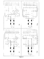
Figure 2 illustrates the paths for currents in an embodiment according to the present invention. -
Figure 1 illustrates a simplified diagram of an inverter according to the present invention. The inverter supplies a grid and comprises a DC link, which comprises two capacitor units in series and a neutral point VDC0 between the capacitor units. The DC link inFigure 1 is supplied by solar cells. The DC link may also be supplied by other types of power sources. The power source may for instance be a fuel cell, a rechargeable battery bank or a boost converter. The converter may also have a galvanic isolation between its input and output. - The inverter further comprises a first inverter leg and a second inverter leg, both legs being connected between the poles Voc+ and VDC- of the DC link. Both inverter legs comprise four switching devices S n1 - S n4 (n∈ {1,2}) connected in series. Each switching device S n1 - S n4 has a conducting state and a non-conducting state and the switching devices S n1 - S n4 together form a low resistance route from the positive pole of the DC link to the negative pole of the DC link when all switching devices S n1 - S n4 are in the conducting state. The switching devices S n1 - S n4 may be for instance IGBTs, as in
Figure 2 , or power MOSFETs. In this embodiment each switching device S11 - S14 and S21 - S24 is paired with a freewheeling diode. In some embodiments of the present invention, some of the switching devices may be IGBTs and some power MOSFETs. - Both inverter legs comprise an upper connection point V n12 between the two topmost switching devices S n1 and S n2, a lower connection point V n34 between the two bottommost switching devices S n3 and S n4 and an output V n23 between the two middle switching devices S n2 and Sn3. The output is filtered with a balanced LCL filter.
- The inverter legs are clamped to the neutral point VDC0. Both inverter legs comprise a first rectifier device D n1 which is connected between the DC link neutral point VDC0 and the leg upper connection point Vn12 allowing flow of current from the DC link neutral point VDC0 to the leg upper connection point V n12, and a second rectifier device D n2 connected between the DC link neutral point VDC0 and the leg lower connection point V n34 allowing flow of current from the leg lower connection point V n34 to the DC link neutral point VDC0. The first rectifier device D n1 and second rectifier D n2 device tie the output V n23 of each inverter leg to the neutral point in the neutral point zero state.
- The inverter legs are clamped also from the output line side. Both inverter legs comprise a third rectifier D n3 device connected between the upper connection point V n12 of the leg and the output V m23 (m ∈ {1,2}, m ≠ n) of the other leg allowing flow of current from the output V m23 of the other leg to the leg upper connection point V n12. and a fourth rectifier device D n4 connected between the output V m23 of the other leg and the lower connection point V n34 of the leg allowing flow of current from the lower connection point V n34 to the output V m23 of the other leg.
- The third rectifier D n3 and fourth rectifier D n4, in co-operation with the inverter leg middle switches S n2 and S n3, provide a path for current which has only two power semiconductors: a diode D n3 or D n4 and a switch S n2 or S n3, respectively.
Table 1 below illustrates a 3-level (line-to-line) output voltage modulation scheme for an embodiment according to the present invention. The scheme has five switching states: +UDC, +0, ±0, -0 and -UDC, represented in Table 1 by five main columns labelled respectively. The rows of the table represent the states of the individual switches. "1" stands for the conducting state and "0" for the non-conducting state.
Table 1. A modulation scheme for the present invention+UDC +0 ±0 -0 -UDC S11 1 0 0 0 0 S12 1 1 1 0 0 S 130 0 1 1 1 S 140 0 0 0 1 S 210 0 0 0 1 S 220 0 1 1 1 S23 1 1 1 0 0 S24 1 0 0 0 0 - The voltage between the inverter leg outputs can in this modulation scheme be set to three potentials: +UDC, 0 and -UDC , where UDC is the voltage potential of the DC link and 0 is zero potential. Each of these potentials can be formed without changes in common-mode voltage.
- The potentials +UDC and -UDc are formed by using states +UDC and -UDC, respectively. The upmost switching devices S n1 and S n2 of an inverter leg and the two bottommost switching devices S n3 and S n4 of the other inverter leg are set to a conducting state, as shown in Table 1. The switching devices provide a path for current from the DC link to the grid. In
Figure 2 , a section denoted with +UDC illustrates the route a for current in the state +UDC. Similarly, a section denoted with -UDC illustrates the route b for current in the state -UDC. - The zero
potential 0 is formed using one of three neutral point zero states +0, ±0 or -0. The state +0 provides two paths for current in the same direction as in state +UDC. The routes c and d for current in the state +0 are illustrated in section +0 ofFigure 2 . In a similar manner, the state -0 provides two paths for current in the same direction as in state -UDC. The routes e and f for current in the state -0 are illustrated in section -0 ofFigure 2 . The state ±0 provides the same paths c, d, e and f as states +0 and -0 together. - It is also possible to form neutral point zero states with one path for current. In a zero state, a neutral point zero state with one current path (c, d, e or f) may be formed by setting only one of the middle switching devices S12, S 13, S22 or S23 to a conducting state.
- Other combinations of routes for current in the neutral point zero state are also possible. For instance, both middle switching devices of an inverter leg may be set to a conducting state. The leg thus provides routes to both directions of current.
- In case the DC link of an inverter according to the present invention is supplied by a switching converter with galvanic isolation, modulation methods with 5-level output voltage (line-to-line) may be used, since the galvanic isolation effectively prevents the common-mode voltages from advancing to the grid side.
- Other modulation methods and switching combinations may also be used to control embodiments according to the present invention.
- It will be obvious to a person skilled in the art that the inventive concept can be implemented in various ways. The invention and its embodiments are not limited to the examples described above but may vary within the scope of the claims.
Claims (12)
- An inverter for supplying a grid, where the inverter comprises
a DC link comprising two capacitor units in series and a neutral point (VDC0) between the capacitor units, and
a first and a second inverter leg, both inverter legs being connected between the poles (VC+ and VDC-) of the DC link and both inverter legs comprising
four switching devices (S n1 - S n4) connected in series, each switch having a conductive state and a non-conductive state and the switches together forming a low resistance route from the positive pole of the DC link to the negative pole of the DC link when all are in the conducting state,
an upper connection point (V n12) between the two topmost switching devices (S n1, S n2),
a lower connection point (V n34) between the two bottommost switching devices (S n3, S n4),
an output (V n23) between the two middle switching devices (S n2, S n3),
a first rectifier device (D n1) connected between the DC link neutral point (VDC0) and the leg upper connection point (V n12) allowing flow of current from the DC link neutral point (VDC0) to the leg upper connection point (V n12), and
a second rectifier device (D n2) connected between the DC link neutral point (VDC0) and the leg lower connection point (V n34) allowing flow of current from the leg lower connection point (V n34) to the DC link neutral point (VDC0),
characterized by each inverter leg further comprising
a third rectifier device (D n3) connected the between upper connection point (V n12) of the leg and the output (V m23) of the other leg allowing flow of current from the output (V m23) of the other leg to the leg upper connection point (V n12), and
a fourth rectifier device (D n4) connected between the output (V m23) of the other leg and the lower connection point (V n34) of the leg allowing flow of current from the lower connection point (V n34) to the output (V m23) of the other leg. - An inverter according to claim 1, characterized in that the switching devices are all IGBTs or all power MOSFETs.
- An inverter according to claim 1, characterized in that some of the switching devices are IGBTs and some of the switching devices are power MOSFETs.
- An arrangement comprising an inverter according to any of claims 1 to 3, characterized in that the DC link of the inverter is supplied by a switching converter, which has a galvanic isolation between its input and output.
- An arrangement comprising an inverter according to any of claims 1 to 3, characterized in that the DC link of the inverter is supplied by a solar generator.
- An arrangement comprising an inverter according to any of claims 1 to 3, characterized in that the DC link of the inverter is supplied by fuel cells.
- An arrangement comprising an inverter according to any of claims 1 to 3, characterized in that the DC link of the inverter is supplied by a rechargeable battery or a rechargeable battery bank.
- An arrangement comprising an inverter according to any of claims 1 to 3, characterized in that the DC link of the inverter is supplied by a boost converter.
- An inverter according to claim 1, characterized in that each switching device is paired with a freewheeling diode.
- A method for controlling an inverter according to claim 1, characterized in that the method comprises a step of
setting one or more of the middle switching devices to conducting state so that the inverter is set to a neutral point zero state. - A method according to claim 10, characterized in that the method comprises a step of
setting the inverter to a neutral point zero state where the current has one path. - A method according to claim 10, characterized in that the method uses only switching states which have same common-mode voltage.
Priority Applications (4)
| Application Number | Priority Date | Filing Date | Title |
|---|---|---|---|
| EP10173154.5A EP2421141B1 (en) | 2010-08-18 | 2010-08-18 | Line and neutral point clamped inverter |
| BR112013003462A BR112013003462A2 (en) | 2010-08-18 | 2011-07-14 | anti-dandruff shampoo and use of an acyl grease isethionate product |
| US13/208,995 US20120044730A1 (en) | 2010-08-18 | 2011-08-12 | Line and neutral point clamped inverter |
| CN2011102510077A CN102377196A (en) | 2010-08-18 | 2011-08-16 | Line and neutral point clamped inverter |
Applications Claiming Priority (1)
| Application Number | Priority Date | Filing Date | Title |
|---|---|---|---|
| EP10173154.5A EP2421141B1 (en) | 2010-08-18 | 2010-08-18 | Line and neutral point clamped inverter |
Publications (2)
| Publication Number | Publication Date |
|---|---|
| EP2421141A1 true EP2421141A1 (en) | 2012-02-22 |
| EP2421141B1 EP2421141B1 (en) | 2013-05-15 |
Family
ID=43533122
Family Applications (1)
| Application Number | Title | Priority Date | Filing Date |
|---|---|---|---|
| EP10173154.5A Not-in-force EP2421141B1 (en) | 2010-08-18 | 2010-08-18 | Line and neutral point clamped inverter |
Country Status (4)
| Country | Link |
|---|---|
| US (1) | US20120044730A1 (en) |
| EP (1) | EP2421141B1 (en) |
| CN (1) | CN102377196A (en) |
| BR (1) | BR112013003462A2 (en) |
Cited By (4)
| Publication number | Priority date | Publication date | Assignee | Title |
|---|---|---|---|---|
| EP2651025A1 (en) * | 2012-04-10 | 2013-10-16 | ABB Oy | 3-level fullbridge NPC inverter assembly for connection to a single phase grid and photovoltaic power plant comprising the same |
| KR101444865B1 (en) * | 2013-08-22 | 2014-10-02 | 삼성중공업 주식회사 | Leg performance test device |
| KR101501118B1 (en) * | 2014-04-08 | 2015-03-19 | 아주대학교산학협력단 | Diagnosis apparatus and method of open switch fault of back to back converter of npc type topology |
| WO2017069333A1 (en) * | 2015-10-22 | 2017-04-27 | 월드탑텍(주) | Dc/dc converter using multi-topology |
Families Citing this family (5)
| Publication number | Priority date | Publication date | Assignee | Title |
|---|---|---|---|---|
| JP5949932B2 (en) * | 2012-10-17 | 2016-07-13 | 株式会社村田製作所 | Inverter device |
| KR101791288B1 (en) * | 2013-06-05 | 2017-10-27 | 엘에스산전 주식회사 | Multi-level inverter |
| DE102015104554A1 (en) * | 2014-05-16 | 2015-11-19 | Semikron Elektronik Gmbh & Co. Kg | circuitry |
| US9997917B2 (en) * | 2015-07-01 | 2018-06-12 | Google Llc | Transformerless power conversion |
| CN113783453B (en) * | 2021-09-29 | 2023-07-07 | 山东建筑大学 | A low-cost high-gain three-level inverter and its space vector modulation method |
Citations (2)
| Publication number | Priority date | Publication date | Assignee | Title |
|---|---|---|---|---|
| US20080298103A1 (en) * | 2007-06-01 | 2008-12-04 | Drs Power & Control Technologies, Inc. | Four pole neutral-point clamped three phase converter with low common mode voltage output |
| DE202010000284U1 (en) * | 2009-03-02 | 2010-05-06 | Abb Research Ltd. | Five-point inverter |
Family Cites Families (3)
| Publication number | Priority date | Publication date | Assignee | Title |
|---|---|---|---|---|
| US7372709B2 (en) * | 2003-09-11 | 2008-05-13 | The Board Of Trustees Of The University Of Illinois | Power conditioning system for energy sources |
| US7430132B2 (en) * | 2006-02-17 | 2008-09-30 | Toshiba International Corporation | Medium voltage inverter system |
| CN101795082B (en) * | 2010-02-05 | 2012-01-11 | 保定天威集团有限公司 | Megawatt direct-drive wind power grid-connection soft-switching converter |
-
2010
- 2010-08-18 EP EP10173154.5A patent/EP2421141B1/en not_active Not-in-force
-
2011
- 2011-07-14 BR BR112013003462A patent/BR112013003462A2/en not_active IP Right Cessation
- 2011-08-12 US US13/208,995 patent/US20120044730A1/en not_active Abandoned
- 2011-08-16 CN CN2011102510077A patent/CN102377196A/en active Pending
Patent Citations (2)
| Publication number | Priority date | Publication date | Assignee | Title |
|---|---|---|---|---|
| US20080298103A1 (en) * | 2007-06-01 | 2008-12-04 | Drs Power & Control Technologies, Inc. | Four pole neutral-point clamped three phase converter with low common mode voltage output |
| DE202010000284U1 (en) * | 2009-03-02 | 2010-05-06 | Abb Research Ltd. | Five-point inverter |
Non-Patent Citations (1)
| Title |
|---|
| AKIRA NABAE ET AL: "A New Neutral-Point-Clamped PWM Inverter", IEEE TRANSACTIONS ON INDUSTRY APPLICATIONS, IEEE SERVICE CENTER, PISCATAWAY, NJ, US, vol. 43, no. 5, 1 September 1981 (1981-09-01), pages 518 - 523, XP011213024, ISSN: 0093-9994 * |
Cited By (5)
| Publication number | Priority date | Publication date | Assignee | Title |
|---|---|---|---|---|
| EP2651025A1 (en) * | 2012-04-10 | 2013-10-16 | ABB Oy | 3-level fullbridge NPC inverter assembly for connection to a single phase grid and photovoltaic power plant comprising the same |
| KR101444865B1 (en) * | 2013-08-22 | 2014-10-02 | 삼성중공업 주식회사 | Leg performance test device |
| KR101501118B1 (en) * | 2014-04-08 | 2015-03-19 | 아주대학교산학협력단 | Diagnosis apparatus and method of open switch fault of back to back converter of npc type topology |
| WO2017069333A1 (en) * | 2015-10-22 | 2017-04-27 | 월드탑텍(주) | Dc/dc converter using multi-topology |
| US10348209B2 (en) | 2015-10-22 | 2019-07-09 | World Toptec Co., Ltd. | Output voltage responsive isolated DC to DC converter in full and half bridge modes |
Also Published As
| Publication number | Publication date |
|---|---|
| US20120044730A1 (en) | 2012-02-23 |
| EP2421141B1 (en) | 2013-05-15 |
| BR112013003462A2 (en) | 2016-08-30 |
| CN102377196A (en) | 2012-03-14 |
Similar Documents
| Publication | Publication Date | Title |
|---|---|---|
| EP2421141B1 (en) | Line and neutral point clamped inverter | |
| US11482947B2 (en) | Efficient switching for converter circuit | |
| Ahmad et al. | Single phase transformerless inverter topology with reduced leakage current for grid connected photovoltaic system | |
| CN107210684B (en) | Five-level topology unit and five-level inverter | |
| US10389268B2 (en) | AC-DC power conversion device including helically cascaded unit cells | |
| US20090244936A1 (en) | Three-phase inverter | |
| EP2651025A1 (en) | 3-level fullbridge NPC inverter assembly for connection to a single phase grid and photovoltaic power plant comprising the same | |
| KR20120136245A (en) | Photovoltaic power conversion apparatus | |
| WO2014111595A1 (en) | A multilevel converter with hybrid full-bridge cells | |
| Vazquez et al. | H5-HERIC based transformerless multilevel inverter for single-phase grid connected PV systems | |
| CN106031011A (en) | Modular Multilevel Converter Branch, Converter and Hybrid Converter Topologies with Flat-Hat PWM Modulation | |
| US20140078802A1 (en) | Dc/ac inverter to convert dc current/voltage to ac current/voltage | |
| CN102130623A (en) | Improved main circuit structure of photovoltaic synchronization inverter | |
| Ardashir et al. | S4 grid-connected single-phase transformerless inverter for PV application | |
| US20140119083A1 (en) | Dc/ac converter, power generation plant and operating method for a dc/ac converter | |
| CN104883084A (en) | Neutral-point clamped cascade H-bridge hybrid multilevel converter | |
| Sireesha et al. | Generalized cascaded multi level inverter using reduced number of components with PV systems | |
| CN104883072A (en) | Transformerless ac-dc-ac cascade multilevel converter | |
| Orfanoudakis et al. | Single-phase transformerless PV inverter topology with AC bypass and mid-DC-link voltage clamping | |
| RU172897U1 (en) | Three Phase Uninterruptible Power Supply | |
| Mohammadi | Analysis of transformerless single-phase inverters in PV grid-connected application | |
| Mondol et al. | A New Cross-Six Inverter for Transformerless Grid-Connected Photovoltaic Systems | |
| CN105262359B (en) | Photovoltaic conversion circuit and photovoltaic electric power equipment | |
| CN104506052A (en) | Three-level semiconductor module, laminated copper bar, phase element circuit and convertor | |
| CN102857131A (en) | Three-phase voltage source converter |
Legal Events
| Date | Code | Title | Description |
|---|---|---|---|
| AK | Designated contracting states |
Kind code of ref document: A1 Designated state(s): AL AT BE BG CH CY CZ DE DK EE ES FI FR GB GR HR HU IE IS IT LI LT LU LV MC MK MT NL NO PL PT RO SE SI SK SM TR |
|
| AX | Request for extension of the european patent |
Extension state: BA ME RS |
|
| PUAI | Public reference made under article 153(3) epc to a published international application that has entered the european phase |
Free format text: ORIGINAL CODE: 0009012 |
|
| 17P | Request for examination filed |
Effective date: 20120402 |
|
| GRAP | Despatch of communication of intention to grant a patent |
Free format text: ORIGINAL CODE: EPIDOSNIGR1 |
|
| GRAS | Grant fee paid |
Free format text: ORIGINAL CODE: EPIDOSNIGR3 |
|
| GRAA | (expected) grant |
Free format text: ORIGINAL CODE: 0009210 |
|
| AK | Designated contracting states |
Kind code of ref document: B1 Designated state(s): AL AT BE BG CH CY CZ DE DK EE ES FI FR GB GR HR HU IE IS IT LI LT LU LV MC MK MT NL NO PL PT RO SE SI SK SM TR |
|
| REG | Reference to a national code |
Ref country code: CH Ref legal event code: EP Ref country code: GB Ref legal event code: FG4D |
|
| REG | Reference to a national code |
Ref country code: AT Ref legal event code: REF Ref document number: 612552 Country of ref document: AT Kind code of ref document: T Effective date: 20130615 |
|
| REG | Reference to a national code |
Ref country code: IE Ref legal event code: FG4D |
|
| REG | Reference to a national code |
Ref country code: DE Ref legal event code: R096 Ref document number: 602010007049 Country of ref document: DE Effective date: 20130711 |
|
| REG | Reference to a national code |
Ref country code: AT Ref legal event code: MK05 Ref document number: 612552 Country of ref document: AT Kind code of ref document: T Effective date: 20130515 |
|
| REG | Reference to a national code |
Ref country code: LT Ref legal event code: MG4D |
|
| REG | Reference to a national code |
Ref country code: NL Ref legal event code: VDEP Effective date: 20130515 |
|
| PG25 | Lapsed in a contracting state [announced via postgrant information from national office to epo] |
Ref country code: NO Free format text: LAPSE BECAUSE OF FAILURE TO SUBMIT A TRANSLATION OF THE DESCRIPTION OR TO PAY THE FEE WITHIN THE PRESCRIBED TIME-LIMIT Effective date: 20130815 Ref country code: LT Free format text: LAPSE BECAUSE OF FAILURE TO SUBMIT A TRANSLATION OF THE DESCRIPTION OR TO PAY THE FEE WITHIN THE PRESCRIBED TIME-LIMIT Effective date: 20130515 Ref country code: PT Free format text: LAPSE BECAUSE OF FAILURE TO SUBMIT A TRANSLATION OF THE DESCRIPTION OR TO PAY THE FEE WITHIN THE PRESCRIBED TIME-LIMIT Effective date: 20130916 Ref country code: GR Free format text: LAPSE BECAUSE OF FAILURE TO SUBMIT A TRANSLATION OF THE DESCRIPTION OR TO PAY THE FEE WITHIN THE PRESCRIBED TIME-LIMIT Effective date: 20130816 Ref country code: AT Free format text: LAPSE BECAUSE OF FAILURE TO SUBMIT A TRANSLATION OF THE DESCRIPTION OR TO PAY THE FEE WITHIN THE PRESCRIBED TIME-LIMIT Effective date: 20130515 Ref country code: ES Free format text: LAPSE BECAUSE OF FAILURE TO SUBMIT A TRANSLATION OF THE DESCRIPTION OR TO PAY THE FEE WITHIN THE PRESCRIBED TIME-LIMIT Effective date: 20130826 Ref country code: SE Free format text: LAPSE BECAUSE OF FAILURE TO SUBMIT A TRANSLATION OF THE DESCRIPTION OR TO PAY THE FEE WITHIN THE PRESCRIBED TIME-LIMIT Effective date: 20130515 Ref country code: SI Free format text: LAPSE BECAUSE OF FAILURE TO SUBMIT A TRANSLATION OF THE DESCRIPTION OR TO PAY THE FEE WITHIN THE PRESCRIBED TIME-LIMIT Effective date: 20130515 Ref country code: IS Free format text: LAPSE BECAUSE OF FAILURE TO SUBMIT A TRANSLATION OF THE DESCRIPTION OR TO PAY THE FEE WITHIN THE PRESCRIBED TIME-LIMIT Effective date: 20130915 |
|
| PGFP | Annual fee paid to national office [announced via postgrant information from national office to epo] |
Ref country code: FI Payment date: 20130813 Year of fee payment: 4 |
|
| PG25 | Lapsed in a contracting state [announced via postgrant information from national office to epo] |
Ref country code: BG Free format text: LAPSE BECAUSE OF FAILURE TO SUBMIT A TRANSLATION OF THE DESCRIPTION OR TO PAY THE FEE WITHIN THE PRESCRIBED TIME-LIMIT Effective date: 20130815 Ref country code: PL Free format text: LAPSE BECAUSE OF FAILURE TO SUBMIT A TRANSLATION OF THE DESCRIPTION OR TO PAY THE FEE WITHIN THE PRESCRIBED TIME-LIMIT Effective date: 20130515 Ref country code: HR Free format text: LAPSE BECAUSE OF FAILURE TO SUBMIT A TRANSLATION OF THE DESCRIPTION OR TO PAY THE FEE WITHIN THE PRESCRIBED TIME-LIMIT Effective date: 20130515 |
|
| PGFP | Annual fee paid to national office [announced via postgrant information from national office to epo] |
Ref country code: FR Payment date: 20130823 Year of fee payment: 4 |
|
| PG25 | Lapsed in a contracting state [announced via postgrant information from national office to epo] |
Ref country code: LV Free format text: LAPSE BECAUSE OF FAILURE TO SUBMIT A TRANSLATION OF THE DESCRIPTION OR TO PAY THE FEE WITHIN THE PRESCRIBED TIME-LIMIT Effective date: 20130515 |
|
| PGFP | Annual fee paid to national office [announced via postgrant information from national office to epo] |
Ref country code: IT Payment date: 20130831 Year of fee payment: 4 |
|
| PG25 | Lapsed in a contracting state [announced via postgrant information from national office to epo] |
Ref country code: DK Free format text: LAPSE BECAUSE OF FAILURE TO SUBMIT A TRANSLATION OF THE DESCRIPTION OR TO PAY THE FEE WITHIN THE PRESCRIBED TIME-LIMIT Effective date: 20130515 Ref country code: CZ Free format text: LAPSE BECAUSE OF FAILURE TO SUBMIT A TRANSLATION OF THE DESCRIPTION OR TO PAY THE FEE WITHIN THE PRESCRIBED TIME-LIMIT Effective date: 20130515 Ref country code: EE Free format text: LAPSE BECAUSE OF FAILURE TO SUBMIT A TRANSLATION OF THE DESCRIPTION OR TO PAY THE FEE WITHIN THE PRESCRIBED TIME-LIMIT Effective date: 20130515 Ref country code: BE Free format text: LAPSE BECAUSE OF FAILURE TO SUBMIT A TRANSLATION OF THE DESCRIPTION OR TO PAY THE FEE WITHIN THE PRESCRIBED TIME-LIMIT Effective date: 20130515 Ref country code: SK Free format text: LAPSE BECAUSE OF FAILURE TO SUBMIT A TRANSLATION OF THE DESCRIPTION OR TO PAY THE FEE WITHIN THE PRESCRIBED TIME-LIMIT Effective date: 20130515 |
|
| PG25 | Lapsed in a contracting state [announced via postgrant information from national office to epo] |
Ref country code: RO Free format text: LAPSE BECAUSE OF FAILURE TO SUBMIT A TRANSLATION OF THE DESCRIPTION OR TO PAY THE FEE WITHIN THE PRESCRIBED TIME-LIMIT Effective date: 20130515 Ref country code: NL Free format text: LAPSE BECAUSE OF FAILURE TO SUBMIT A TRANSLATION OF THE DESCRIPTION OR TO PAY THE FEE WITHIN THE PRESCRIBED TIME-LIMIT Effective date: 20130515 |
|
| PLBE | No opposition filed within time limit |
Free format text: ORIGINAL CODE: 0009261 |
|
| STAA | Information on the status of an ep patent application or granted ep patent |
Free format text: STATUS: NO OPPOSITION FILED WITHIN TIME LIMIT |
|
| 26N | No opposition filed |
Effective date: 20140218 |
|
| PG25 | Lapsed in a contracting state [announced via postgrant information from national office to epo] |
Ref country code: MC Free format text: LAPSE BECAUSE OF FAILURE TO SUBMIT A TRANSLATION OF THE DESCRIPTION OR TO PAY THE FEE WITHIN THE PRESCRIBED TIME-LIMIT Effective date: 20130515 |
|
| REG | Reference to a national code |
Ref country code: IE Ref legal event code: MM4A |
|
| REG | Reference to a national code |
Ref country code: DE Ref legal event code: R097 Ref document number: 602010007049 Country of ref document: DE Effective date: 20140218 |
|
| PG25 | Lapsed in a contracting state [announced via postgrant information from national office to epo] |
Ref country code: IE Free format text: LAPSE BECAUSE OF NON-PAYMENT OF DUE FEES Effective date: 20130818 |
|
| PGFP | Annual fee paid to national office [announced via postgrant information from national office to epo] |
Ref country code: DE Payment date: 20130821 Year of fee payment: 4 |
|
| REG | Reference to a national code |
Ref country code: DE Ref legal event code: R119 Ref document number: 602010007049 Country of ref document: DE |
|
| REG | Reference to a national code |
Ref country code: CH Ref legal event code: PL |
|
| GBPC | Gb: european patent ceased through non-payment of renewal fee |
Effective date: 20140818 |
|
| PG25 | Lapsed in a contracting state [announced via postgrant information from national office to epo] |
Ref country code: IT Free format text: LAPSE BECAUSE OF NON-PAYMENT OF DUE FEES Effective date: 20140818 Ref country code: FI Free format text: LAPSE BECAUSE OF NON-PAYMENT OF DUE FEES Effective date: 20140818 Ref country code: LI Free format text: LAPSE BECAUSE OF NON-PAYMENT OF DUE FEES Effective date: 20140831 Ref country code: CH Free format text: LAPSE BECAUSE OF NON-PAYMENT OF DUE FEES Effective date: 20140831 |
|
| REG | Reference to a national code |
Ref country code: DE Ref legal event code: R119 Ref document number: 602010007049 Country of ref document: DE Effective date: 20150303 |
|
| PG25 | Lapsed in a contracting state [announced via postgrant information from national office to epo] |
Ref country code: SM Free format text: LAPSE BECAUSE OF FAILURE TO SUBMIT A TRANSLATION OF THE DESCRIPTION OR TO PAY THE FEE WITHIN THE PRESCRIBED TIME-LIMIT Effective date: 20130515 |
|
| REG | Reference to a national code |
Ref country code: FR Ref legal event code: ST Effective date: 20150430 |
|
| PG25 | Lapsed in a contracting state [announced via postgrant information from national office to epo] |
Ref country code: MT Free format text: LAPSE BECAUSE OF FAILURE TO SUBMIT A TRANSLATION OF THE DESCRIPTION OR TO PAY THE FEE WITHIN THE PRESCRIBED TIME-LIMIT Effective date: 20130515 Ref country code: TR Free format text: LAPSE BECAUSE OF FAILURE TO SUBMIT A TRANSLATION OF THE DESCRIPTION OR TO PAY THE FEE WITHIN THE PRESCRIBED TIME-LIMIT Effective date: 20130515 Ref country code: CY Free format text: LAPSE BECAUSE OF FAILURE TO SUBMIT A TRANSLATION OF THE DESCRIPTION OR TO PAY THE FEE WITHIN THE PRESCRIBED TIME-LIMIT Effective date: 20130515 |
|
| PG25 | Lapsed in a contracting state [announced via postgrant information from national office to epo] |
Ref country code: GB Free format text: LAPSE BECAUSE OF NON-PAYMENT OF DUE FEES Effective date: 20140818 Ref country code: DE Free format text: LAPSE BECAUSE OF NON-PAYMENT OF DUE FEES Effective date: 20150303 Ref country code: HU Free format text: LAPSE BECAUSE OF FAILURE TO SUBMIT A TRANSLATION OF THE DESCRIPTION OR TO PAY THE FEE WITHIN THE PRESCRIBED TIME-LIMIT; INVALID AB INITIO Effective date: 20100818 Ref country code: MK Free format text: LAPSE BECAUSE OF FAILURE TO SUBMIT A TRANSLATION OF THE DESCRIPTION OR TO PAY THE FEE WITHIN THE PRESCRIBED TIME-LIMIT Effective date: 20130515 Ref country code: LU Free format text: LAPSE BECAUSE OF NON-PAYMENT OF DUE FEES Effective date: 20130818 |
|
| PG25 | Lapsed in a contracting state [announced via postgrant information from national office to epo] |
Ref country code: FR Free format text: LAPSE BECAUSE OF NON-PAYMENT OF DUE FEES Effective date: 20140901 |
|
| PG25 | Lapsed in a contracting state [announced via postgrant information from national office to epo] |
Ref country code: AL Free format text: LAPSE BECAUSE OF FAILURE TO SUBMIT A TRANSLATION OF THE DESCRIPTION OR TO PAY THE FEE WITHIN THE PRESCRIBED TIME-LIMIT Effective date: 20130515 |