EP2418922A1 - Printed circuit board assembly for pots splitters of a VDSL telecommunication system - Google Patents
Printed circuit board assembly for pots splitters of a VDSL telecommunication system Download PDFInfo
- Publication number
- EP2418922A1 EP2418922A1 EP10305853A EP10305853A EP2418922A1 EP 2418922 A1 EP2418922 A1 EP 2418922A1 EP 10305853 A EP10305853 A EP 10305853A EP 10305853 A EP10305853 A EP 10305853A EP 2418922 A1 EP2418922 A1 EP 2418922A1
- Authority
- EP
- European Patent Office
- Prior art keywords
- low
- line interface
- pass filters
- circuit board
- printed circuit
- Prior art date
- Legal status (The legal status is an assumption and is not a legal conclusion. Google has not performed a legal analysis and makes no representation as to the accuracy of the status listed.)
- Granted
Links
- 101100004408 Arabidopsis thaliana BIG gene Proteins 0.000 claims abstract description 21
- 101150017033 LPR1 gene Proteins 0.000 claims abstract description 21
- 101150089216 LPR2 gene Proteins 0.000 claims abstract description 21
- 101100008072 Saccharomyces cerevisiae (strain ATCC 204508 / S288c) CWP2 gene Proteins 0.000 claims abstract description 21
- 101100381996 Saccharomyces cerevisiae (strain ATCC 204508 / S288c) BRO1 gene Proteins 0.000 claims abstract description 20
- 230000000694 effects Effects 0.000 abstract description 8
- 101000615541 Canis lupus familiaris E3 ubiquitin-protein ligase Mdm2 Proteins 0.000 abstract description 5
- 238000011144 upstream manufacturing Methods 0.000 description 1
Images

Classifications
-
- H—ELECTRICITY
- H05—ELECTRIC TECHNIQUES NOT OTHERWISE PROVIDED FOR
- H05K—PRINTED CIRCUITS; CASINGS OR CONSTRUCTIONAL DETAILS OF ELECTRIC APPARATUS; MANUFACTURE OF ASSEMBLAGES OF ELECTRICAL COMPONENTS
- H05K1/00—Printed circuits
- H05K1/02—Details
- H05K1/0213—Electrical arrangements not otherwise provided for
- H05K1/0237—High frequency adaptations
- H05K1/025—Impedance arrangements, e.g. impedance matching, reduction of parasitic impedance
-
- H—ELECTRICITY
- H05—ELECTRIC TECHNIQUES NOT OTHERWISE PROVIDED FOR
- H05K—PRINTED CIRCUITS; CASINGS OR CONSTRUCTIONAL DETAILS OF ELECTRIC APPARATUS; MANUFACTURE OF ASSEMBLAGES OF ELECTRICAL COMPONENTS
- H05K1/00—Printed circuits
- H05K1/02—Details
- H05K1/0213—Electrical arrangements not otherwise provided for
- H05K1/0237—High frequency adaptations
- H05K1/0243—Printed circuits associated with mounted high frequency components
-
- H—ELECTRICITY
- H04—ELECTRIC COMMUNICATION TECHNIQUE
- H04M—TELEPHONIC COMMUNICATION
- H04M11/00—Telephonic communication systems specially adapted for combination with other electrical systems
- H04M11/06—Simultaneous speech and data transmission, e.g. telegraphic transmission over the same conductors
- H04M11/062—Simultaneous speech and data transmission, e.g. telegraphic transmission over the same conductors using different frequency bands for speech and other data
-
- H—ELECTRICITY
- H05—ELECTRIC TECHNIQUES NOT OTHERWISE PROVIDED FOR
- H05K—PRINTED CIRCUITS; CASINGS OR CONSTRUCTIONAL DETAILS OF ELECTRIC APPARATUS; MANUFACTURE OF ASSEMBLAGES OF ELECTRICAL COMPONENTS
- H05K1/00—Printed circuits
- H05K1/02—Details
- H05K1/0213—Electrical arrangements not otherwise provided for
- H05K1/0216—Reduction of cross-talk, noise or electromagnetic interference
- H05K1/023—Reduction of cross-talk, noise or electromagnetic interference using auxiliary mounted passive components or auxiliary substances
- H05K1/0233—Filters, inductors or a magnetic substance
-
- H—ELECTRICITY
- H05—ELECTRIC TECHNIQUES NOT OTHERWISE PROVIDED FOR
- H05K—PRINTED CIRCUITS; CASINGS OR CONSTRUCTIONAL DETAILS OF ELECTRIC APPARATUS; MANUFACTURE OF ASSEMBLAGES OF ELECTRICAL COMPONENTS
- H05K1/00—Printed circuits
- H05K1/02—Details
- H05K1/0213—Electrical arrangements not otherwise provided for
- H05K1/0237—High frequency adaptations
- H05K1/0246—Termination of transmission lines
-
- H—ELECTRICITY
- H05—ELECTRIC TECHNIQUES NOT OTHERWISE PROVIDED FOR
- H05K—PRINTED CIRCUITS; CASINGS OR CONSTRUCTIONAL DETAILS OF ELECTRIC APPARATUS; MANUFACTURE OF ASSEMBLAGES OF ELECTRICAL COMPONENTS
- H05K2201/00—Indexing scheme relating to printed circuits covered by H05K1/00
- H05K2201/10—Details of components or other objects attached to or integrated in a printed circuit board
- H05K2201/10007—Types of components
- H05K2201/10189—Non-printed connector
Definitions
- the present invention relates to a printed circuit board assembly for a Plain Old Telephone System POTS splitter of a VDSL telecommunication system, said assembly comprising a Printed Circuit Board PCB provided with a line interface connector connected to a plurality of low-pass filters on said PCB, said line interface connector being adapted to be coupled to telecommunication lines.
- the impact of the low-pass filters LP1, LP2, ... LPn of the POTS splitter on the VDSL performances of the telecommunication lines needs to be minimized.
- the printed circuit board assembly must be designed in such a way that it's line impedance has no effect on the loading of the VDSL signals that are coming from the telecommunication line, and more particularly from the line termination board thereof.
- this loading effect can result in an attenuation effect of the highest frequencies where it affects the Downstream as well as Upstream VDSLtones. Moreover, it can also have an effect on the matching of the analog front-end towards the line impedance.
- a main problem is that the routing from the line interface connector X1 - X4 to the first component of the low-pass filter LP1, LP2, ... LPn has a capacitive effect on the input impedance of the POTS splitter. As a consequence, the capacity of the differential pairs adds up with the input impedance of the low-pass filter.
- Another problem is the variation in line interface trace lengths on the Printed Circuit Board PCB, mainly between the line interface connector X1 - X4 and the low-pass filters LP1, LP2, ... LPn.
- Different lengths of line interface traces on the low-pass filters give spread on the VDSL performance.
- a VDSL telecommunication line of which the POTS splitter has a short line interface trace towards the low-pass filter can have a good performance.
- this performance can be reduced for a VDSL telecommunication line with a large splitter line interface traces.
- VDSL performance can be influenced by the analog front-end components, it is very hard to adjust performance for all types of trace lengths towards the different low-pass filters.
- the best solution today is to optimize the routing of the differential pair of a VDSL telecommunication line from the line interface connector X1 - X4 towards the low-pass filter LP1, LP2, ... LPn.
- the components of each low-pass filter are grouped together on the PCB in such a way that the distances between these components, as well as the distance to the line interface connector, are as small as physically possible.
- An object of the present invention is to provide a printed circuit board assembly of the above known type but wherein all the low-pass filters on the PCB provide similar POTS splitter performance characteristics with respect to the VDSL telecommunication lines.
- this object is achieved due to the fact that each low-pass filter of said plurality is physically separated into a front stage comprising at least one component of said low-pass filter connected to said line interface connector and into a rear stage comprising other components of said low-pass filter, and that all the front stages of all the low-pass filters of said plurality are physically located on said PCB closer to said line interface connector than said rear stages.
- said component of said front stage is an inductor coupled to said line interface connector.
- line interface connector is further adapted to be coupled to a plurality of analog front end high-pass filters also forming part of said POTS splitters, and that each low-pass filter is associated to a distinct analog front end high-pass filter.
- Each POTS splitter comprises a low-pass filter and an analog front end high-pass filter, also called line transformer.
- the loading effect of the low-pass filter on the VDSL analog front end is reduced by placing the first inductor, also called line side filter coil, of the low-pass filter as close as possible to the high-pass filter.
- the physical length of the connection between the line transformer and the line side filter coil is thereby reduced as well as the Differential Mode Capacitance Cdm1 of the POTS splitter.
- said PCB comprises a plurality of line interface connectors each connected to a distinct plurality of low-pass filters and each adapted to be coupled to telecommunication lines, and all the front stages of all the low-pass filters connected to a predetermined line interface connector are physically located on said PCB closer to said predetermined line interface connector than the rear stages of all these low-pass filters.
- Coupled should not be interpreted as being restricted to direct connections only.
- scope of the expression such as “a device A coupled to a device B” should not be limited to embodiments of a device wherein an output of device A is directly connected to an input of device B. It means that there may exist a path between an output of A and an input of B, which path may include other devices or means.
- the printed circuit board assembly shown at Fig. 2 forms part of Plain Old Telephone System POTS splitter at a Central Office CO of a VDSL telecommunication system.
- each POTS splitter comprises a low-pass filter LPF1, LPR1; LPF2, LPR2; ... LPFn, LPRn and an analog front end high-pass filter (not shown), also called line transformer.
- the printed circuit board assembly comprises a Printed Circuit Board PCB, also called POTS splitter daughterboard, provided with, e.g. 4, groups of 12 low-pass filters, each group of low-pass filters being connected to a distinct line interface connector X1 to X4 also on the PCB.
- a Printed Circuit Board PCB also called POTS splitter daughterboard, provided with, e.g. 4, groups of 12 low-pass filters, each group of low-pass filters being connected to a distinct line interface connector X1 to X4 also on the PCB.
- the 4 line interface connectors X1 - X4 are connected to a line termination VDSL motherboard (not shown) housing the high-pass filters of the splitters.
- the line termination VDSL motherboard is further connected, together with the 4 line interface connectors X1 - X4, to 48 telecommunication lines towards Customer Premise Equipment CPE.
- the loading effect of each POTS splitter on the VDSL analog front end must be reduced is such a way that the Differential Mode Capacitance Cdm1, Cdm2, ... Cdmn of the line interface track towards the customer is smaller than 3pF.
- the PCB of the printed circuit board assembly has a particular layout, as the embodiment of the invention shown at Fig. 2 , wherein all the lines of the Central Office CO POTS splitters are within the 3pF trace length.
- each low-pass filter LPF1, LPR1; LPF2, LPR2; ... LPFn, LPRn of the POTS splitters on the PCB is physically separated or splitted in a front stage LPF1; LPF2; ... LPFn and a rear stage LPR1; LPR2; ... LPRn.
- the front stage LPF1; LPF2; ... LPFn comprises at least one component, preferably the first inductor, also called line side filter coil, of the low-pass filter connected to the line interface connector.
- This front stage LPF1; LPF2; ... LPFn is physically located on the PCB as close as possible to the line interface connector, here X1 but identical for X2, X3 and X4, and thereby to the high-pass filter of the splitter on the line termination VDSL motherboard.
- the front stage LPF1; LPF2; ... LPFn of the low-pass filter can be placed within the 3pF trace length from the line interface connector, i.e. in the condition where Cdm1; Cdm2; ... Cdmn is smaller than 3pF.
- the rear stages LPR1; LPR2; ... LPRn of the low-pass filters are all connected to a POTS interface connector X10 provided of the PCB.
- This POTS interface connector X10 is further coupled to a POTS interface of a local exchange.
- the location of the rear stage LPR1; LPR2; ... LPRn on the PCB is less important as these only carry the base band frequencies, whereby the requirements with respect to the rear stage LPR1; LPR2; ... LPRn are less stringent.
- the front stages LPF1; LPF2; ... LPFn of all the low-pass filters are coupled to the line interface connector X1 - X4 via line interface traces all having substantially the same length. Furthermore, the physical length of the connection between the line transformer and the line side filter coil is thereby also reduced, which positively further affects the Differential Mode Capacitance Cdm1; Cdm2; ... Cdmn.
Landscapes
- Engineering & Computer Science (AREA)
- Microelectronics & Electronic Packaging (AREA)
- Filters And Equalizers (AREA)
- Telephonic Communication Services (AREA)
Abstract
Description
- The present invention relates to a printed circuit board assembly for a Plain Old Telephone System POTS splitter of a VDSL telecommunication system, said assembly comprising a Printed Circuit Board PCB provided with a line interface connector connected to a plurality of low-pass filters on said PCB, said line interface connector being adapted to be coupled to telecommunication lines.
- On such a printed circuit board assembly, e.g. as illustrated at
Fig. 1 , the impact of the low-pass filters LP1, LP2, ... LPn of the POTS splitter on the VDSL performances of the telecommunication lines needs to be minimized. In other words, the printed circuit board assembly must be designed in such a way that it's line impedance has no effect on the loading of the VDSL signals that are coming from the telecommunication line, and more particularly from the line termination board thereof. - Indeed, this loading effect can result in an attenuation effect of the highest frequencies where it affects the Downstream as well as Upstream VDSLtones. Moreover, it can also have an effect on the matching of the analog front-end towards the line impedance.
- A main problem is that the routing from the line interface connector X1 - X4 to the first component of the low-pass filter LP1, LP2, ... LPn has a capacitive effect on the input impedance of the POTS splitter. As a consequence, the capacity of the differential pairs adds up with the input impedance of the low-pass filter.
- Another problem is the variation in line interface trace lengths on the Printed Circuit Board PCB, mainly between the line interface connector X1 - X4 and the low-pass filters LP1, LP2, ... LPn. Different lengths of line interface traces on the low-pass filters give spread on the VDSL performance. There is a short line interface trace when the low-pass filter is located near the line interface connector and a long line interface trace when the low-pass filter is located near the board edge of the PCB. A VDSL telecommunication line of which the POTS splitter has a short line interface trace towards the low-pass filter can have a good performance. However, this performance can be reduced for a VDSL telecommunication line with a large splitter line interface traces. This is due to the large Differential Mode Capacitance Cdm1, Cdm2, ... Cdmn of the low-pass filter. Although VDSL performance can be influenced by the analog front-end components, it is very hard to adjust performance for all types of trace lengths towards the different low-pass filters.
- The best solution today is to optimize the routing of the differential pair of a VDSL telecommunication line from the line interface connector X1 - X4 towards the low-pass filter LP1, LP2, ... LPn. The components of each low-pass filter are grouped together on the PCB in such a way that the distances between these components, as well as the distance to the line interface connector, are as small as physically possible.
- However, bearing in mind that an entire printed circuit board assembly or POTS splitter board is coupled to several lines, e.g. 48 differential pairs of VDSL telecommunication lines, it is obvious that not all low-pass filters LP1, LP2, ... LPn can have the same distance to the line interface connector X1 - X4 and that the line interface trace length towards the line interface connector can be very long if the low-pass filter, e.g. LP1, is situated, in a worst case, at the edge of the printed circuit board PCB. In that case, the capacitive load of the differential pair can be very high and adds up with the low-pass filter input impedance. This will result in a very bad VDSL performance impact.
- An object of the present invention is to provide a printed circuit board assembly of the above known type but wherein all the low-pass filters on the PCB provide similar POTS splitter performance characteristics with respect to the VDSL telecommunication lines.
- According to a characterizing embodiment, this object is achieved due to the fact that each low-pass filter of said plurality is physically separated into a front stage comprising at least one component of said low-pass filter connected to said line interface connector and into a rear stage comprising other components of said low-pass filter, and that all the front stages of all the low-pass filters of said plurality are physically located on said PCB closer to said line interface connector than said rear stages.
- In this way, the front stages of all the low-pass filters are coupled to the line interface connector via line interface traces having all a similar length. As a result, the performance characteristics of the corresponding POTS splitters are substantially identical.
- Another characterizing embodiment is that said component of said front stage is an inductor coupled to said line interface connector.
- Also another characterizing embodiment is that said line interface connector is further adapted to be coupled to a plurality of analog front end high-pass filters also forming part of said POTS splitters, and that each low-pass filter is associated to a distinct analog front end high-pass filter.
- Each POTS splitter comprises a low-pass filter and an analog front end high-pass filter, also called line transformer. The loading effect of the low-pass filter on the VDSL analog front end is reduced by placing the first inductor, also called line side filter coil, of the low-pass filter as close as possible to the high-pass filter. The physical length of the connection between the line transformer and the line side filter coil is thereby reduced as well as the Differential Mode Capacitance Cdm1 of the POTS splitter.
- In a preferred characterizing embodiment, said PCB comprises a plurality of line interface connectors each connected to a distinct plurality of low-pass filters and each adapted to be coupled to telecommunication lines, and all the front stages of all the low-pass filters connected to a predetermined line interface connector are physically located on said PCB closer to said predetermined line interface connector than the rear stages of all these low-pass filters.
- In this way, it is for instance possible to place 4 line interface connectors, each connected to 12 front stages of low-pass filters on a same area of the PCB. As a result, 48 POTS splitter lines are available on a limited PCB board space without influencing the performance, e.g. the bit rate, of the VDSL line termination board.
- Further characterizing embodiments of the present printed circuit board assembly are mentioned in the appended claims.
- It is to be noticed that the terms "comprising" or "including", used in the claims, should not be interpreted as being restricted to the means listed thereafter. Thus, the scope of an expression such as "a device comprising means A and B" should not be limited to an embodiment of a device consisting only of the means A and B. It means that, with respect to embodiments of the present invention, A and B are essential means of the device.
- Similarly, it is to be noticed that the term "coupled", also used in the claims, should not be interpreted as being restricted to direct connections only. Thus, the scope of the expression such as "a device A coupled to a device B" should not be limited to embodiments of a device wherein an output of device A is directly connected to an input of device B. It means that there may exist a path between an output of A and an input of B, which path may include other devices or means.
- The above and other objects and features of the invention will become more apparent and the invention itself will be best understood by referring to the following description of an embodiment taken in conjunction with the accompanying drawings wherein:
-
Fig. 1 is a schematic view of a printed circuit board assembly comprising POTS splitters of a VDSL telecommunication system; and -
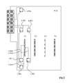
Fig. 2 represents a printed circuit board assembly comprising POTS splitters according to an embodiment of the invention. - Similarly to the printed circuit board assembly showed at
Fig. 1 and described above, the printed circuit board assembly shown atFig. 2 forms part of Plain Old Telephone System POTS splitter at a Central Office CO of a VDSL telecommunication system. - In such a VDSL telecommunication system, each POTS splitter comprises a low-pass filter LPF1, LPR1; LPF2, LPR2; ... LPFn, LPRn and an analog front end high-pass filter (not shown), also called line transformer.
- The printed circuit board assembly comprises a Printed Circuit Board PCB, also called POTS splitter daughterboard, provided with, e.g. 4, groups of 12 low-pass filters, each group of low-pass filters being connected to a distinct line interface connector X1 to X4 also on the PCB.
- The 4 line interface connectors X1 - X4 are connected to a line termination VDSL motherboard (not shown) housing the high-pass filters of the splitters. The line termination VDSL motherboard is further connected, together with the 4 line interface connectors X1 - X4, to 48 telecommunication lines towards Customer Premise Equipment CPE.
- In order to achieve VDSL requirements, the loading effect of each POTS splitter on the VDSL analog front end must be reduced is such a way that the Differential Mode Capacitance Cdm1, Cdm2, ... Cdmn of the line interface track towards the customer is smaller than 3pF. To this end, the PCB of the printed circuit board assembly has a particular layout, as the embodiment of the invention shown at
Fig. 2 , wherein all the lines of the Central Office CO POTS splitters are within the 3pF trace length. - In more detail, each low-pass filter LPF1, LPR1; LPF2, LPR2; ... LPFn, LPRn of the POTS splitters on the PCB is physically separated or splitted in a front stage LPF1; LPF2; ... LPFn and a rear stage LPR1; LPR2; ... LPRn.
- The front stage LPF1; LPF2; ... LPFn comprises at least one component, preferably the first inductor, also called line side filter coil, of the low-pass filter connected to the line interface connector. This front stage LPF1; LPF2; ... LPFn is physically located on the PCB as close as possible to the line interface connector, here X1 but identical for X2, X3 and X4, and thereby to the high-pass filter of the splitter on the line termination VDSL motherboard.
- In this way, the front stage LPF1; LPF2; ... LPFn of the low-pass filter can be placed within the 3pF trace length from the line interface connector, i.e. in the condition where Cdm1; Cdm2; ... Cdmn is smaller than 3pF.
- This layout leaves the rest of the PCB open with enough space to mount all the rear or second stages LPR1; LPR2; ... LPRn of low-pass filters. Each rear stage LPR1; LPR2; ... LPRn comprising the remaining components of the low-pass filter that are not comprised in the front stage thereof.
- The rear stages LPR1; LPR2; ... LPRn of the low-pass filters are all connected to a POTS interface connector X10 provided of the PCB. This POTS interface connector X10 is further coupled to a POTS interface of a local exchange.
- The location of the rear stage LPR1; LPR2; ... LPRn on the PCB is less important as these only carry the base band frequencies, whereby the requirements with respect to the rear stage LPR1; LPR2; ... LPRn are less stringent.
- As a result, the front stages LPF1; LPF2; ... LPFn of all the low-pass filters are coupled to the line interface connector X1 - X4 via line interface traces all having substantially the same length. Furthermore, the physical length of the connection between the line transformer and the line side filter coil is thereby also reduced, which positively further affects the Differential Mode Capacitance Cdm1; Cdm2; ... Cdmn.
- A final remark is that embodiments of the present invention are described above in terms of functional blocks. From the functional description of these blocks, given above, it will be apparent for a person skilled in the art of designing electronic devices how embodiments of these blocks can be manufactured with well-known electronic components. A detailed architecture of the contents of the functional blocks hence is not given.
- While the principles of the invention have been described above in connection with specific apparatus, it is to be clearly understood that this description is merely made by way of example and not as a limitation on the scope of the invention, as defined in the appended claims.
Claims (8)
- A printed circuit board assembly for a Plain Old Telephone System POTS splitter of a VDSL telecommunication system, said assembly comprising a printed circuit board PCB provided with a line interface connector (X1 - X4) connected to a plurality of low-pass filters (LPF1, LPR1; LPF2, LPR2; ... LPFn, LPRn) on said PCB, said line interface connector being adapted to be coupled to telecommunication lines,
characterized in that each low-pass filter of said plurality is physically separated into a front stage (LPF1; LPF2; ... LPFn) comprising at least one component of said low-pass filter (LPF1, LPR1; LPF2, LPR2; ... LPFn, LPRn) connected to said line interface connector (X1 - X4) and into a rear stage (LPR1; LPR2; ... LPRn) comprising other components of said low-pass filter,
and in that all the front stages of all the low-pass filters of said plurality are physically located on said PCB closer to said line interface connector than said rear stages. - The printed circuit board assembly according to claim 1, characterized in that said component of said front stage (LPF1; LPF2; ... LPFn) is an inductor coupled to said line interface connector (X1 - X4).
- The printed circuit board assembly according to claim 1, characterized in that said PCB is further provided with a POTS interface connector (X10) connected to the rear stages (LPR1; LPR2; ... LPRn) of the low-pass filters (LPF1, LPR1; LPF2, LPR2; ... LPFn, LPRn) of said plurality and adapted to be coupled to a POTS interface of a local exchange.
- The printed circuit board assembly according to claim 1, characterized in that said low-pass filter (LPF1, LPR1; LPF2, LPR2; ... LPFn, LPRn) forms part of a POTS splitter located at a Central Office CO of said VDSL telecommunication system.
- The printed circuit board assembly according to claim 1, characterized in that said line interface connector (X1 - X4) is further adapted to be coupled to a plurality of analog front ends high-pass filters forming part of said POTS splitters.
- The printed circuit board assembly according to claim 5, characterized in that each low-pass filter (LPF1, LPR1; LPF2, LPR2; ... LPFn, LPRn) of said plurality of low-pass filters is associated to a distinct analog front end high-pass filter of said plurality of high-pass filters.
- The printed circuit board assembly according to claim 1,
characterized in that all the front stages (LPF1; LPF2; ... LPFn) of all the low-pass filters (LPF1, LPR1; LPF2, LPR2; ... LPFn, LPRn) of said plurality surround said line interface connector (X1 - X4) on a first area of said PCB,
and in that all the rear stages (LPR1; LPR2; ... LPRn) of all the low-pass filters of said plurality are located on a second area of said PCB. - The printed circuit board assembly according to claim 1,
characterized in that said PCB comprises a plurality of line interface connectors (X1 - X4) each connected to a distinct plurality of low-pass filters (LPF1, LPR1; LPF2, LPR2; ... LPFn, LPRn) and each adapted to be coupled to telecommunication lines,
and in that all the front stages (LPF1; LPF2; ... LPFn) of all the low-pass filters of a predetermined plurality of low-pass filters connected to a predetermined line interface connector (X1 - X4) of said plurality of line interface connectors are physically located on said PCB closer to said predetermined line interface connector than the rear stages (LPR1; LPR2; ... LPRn) of all the low-pass filters of said predetermined plurality of low-pass filters.
Priority Applications (1)
| Application Number | Priority Date | Filing Date | Title |
|---|---|---|---|
| EP20100305853 EP2418922B1 (en) | 2010-08-02 | 2010-08-02 | Printed circuit board assembly for POTS-splitters of a VDSL telecommunication system |
Applications Claiming Priority (1)
| Application Number | Priority Date | Filing Date | Title |
|---|---|---|---|
| EP20100305853 EP2418922B1 (en) | 2010-08-02 | 2010-08-02 | Printed circuit board assembly for POTS-splitters of a VDSL telecommunication system |
Publications (3)
| Publication Number | Publication Date |
|---|---|
| EP2418922A1 true EP2418922A1 (en) | 2012-02-15 |
| EP2418922A8 EP2418922A8 (en) | 2012-03-21 |
| EP2418922B1 EP2418922B1 (en) | 2013-04-03 |
Family
ID=43031470
Family Applications (1)
| Application Number | Title | Priority Date | Filing Date |
|---|---|---|---|
| EP20100305853 Not-in-force EP2418922B1 (en) | 2010-08-02 | 2010-08-02 | Printed circuit board assembly for POTS-splitters of a VDSL telecommunication system |
Country Status (1)
| Country | Link |
|---|---|
| EP (1) | EP2418922B1 (en) |
Citations (3)
| Publication number | Priority date | Publication date | Assignee | Title |
|---|---|---|---|---|
| US20020136396A1 (en) * | 2001-03-22 | 2002-09-26 | Witty Amy J. | Insulation strip for a pots splitter card |
| US20030002656A1 (en) * | 2001-06-29 | 2003-01-02 | Adc Telecommunications, Inc. | Splitter assembly with high density backplane board |
| US20030112960A1 (en) * | 2001-12-14 | 2003-06-19 | Adc Dsl Systems, Inc. | Cascade low-pass filter to improve xDSL band attenuation for POTS splitter |
-
2010
- 2010-08-02 EP EP20100305853 patent/EP2418922B1/en not_active Not-in-force
Patent Citations (3)
| Publication number | Priority date | Publication date | Assignee | Title |
|---|---|---|---|---|
| US20020136396A1 (en) * | 2001-03-22 | 2002-09-26 | Witty Amy J. | Insulation strip for a pots splitter card |
| US20030002656A1 (en) * | 2001-06-29 | 2003-01-02 | Adc Telecommunications, Inc. | Splitter assembly with high density backplane board |
| US20030112960A1 (en) * | 2001-12-14 | 2003-06-19 | Adc Dsl Systems, Inc. | Cascade low-pass filter to improve xDSL band attenuation for POTS splitter |
Also Published As
| Publication number | Publication date |
|---|---|
| EP2418922A8 (en) | 2012-03-21 |
| EP2418922B1 (en) | 2013-04-03 |
Similar Documents
| Publication | Publication Date | Title |
|---|---|---|
| US8041010B2 (en) | Splitter card with integral test access | |
| US7596649B2 (en) | Motherboard | |
| CN201336411Y (en) | Bonding pad group for SFP connector and communication device | |
| JPWO2012133755A1 (en) | Transmission system and backplane system construction method | |
| JP6599520B2 (en) | Connector and system having improved crosstalk performance | |
| US9124429B2 (en) | Combination device for DSL phantom mode signals in a telecommunication system | |
| JP4141707B2 (en) | Hybrid circuit for broadband modem | |
| EP2418922A1 (en) | Printed circuit board assembly for pots splitters of a VDSL telecommunication system | |
| US6812805B2 (en) | Differential transmission line for high bandwidth signals | |
| US8467522B2 (en) | Universal ISDN/POTS splitter | |
| US7463472B1 (en) | Signal splitter/surge protector | |
| CN1960196B (en) | A telecommunications filter device | |
| CN102082886A (en) | Circuit and equipment of digital subscriber line | |
| US20140119422A1 (en) | Multi-stage equalizer | |
| EP2066103A1 (en) | Switchable impedance xdsl splitter | |
| US20120092087A1 (en) | Noise reduction device for port of dsl filter and method thereof | |
| AU2006100159A4 (en) | A filter | |
| US20070286408A1 (en) | Module and Connector | |
| US20060018462A1 (en) | Make-before-break ADSL/VDSL splitter card | |
| US20040179674A1 (en) | Attenuator for ADSL signals | |
| JP2002034060A (en) | DSL splitter unit | |
| AU2007100379A4 (en) | A filter | |
| AU2006100490B4 (en) | A filter | |
| EP1901539A1 (en) | DSL splitter |
Legal Events
| Date | Code | Title | Description |
|---|---|---|---|
| AK | Designated contracting states |
Kind code of ref document: A1 Designated state(s): AL AT BE BG CH CY CZ DE DK EE ES FI FR GB GR HR HU IE IS IT LI LT LU LV MC MK MT NL NO PL PT RO SE SI SK SM TR |
|
| AX | Request for extension of the european patent |
Extension state: BA ME RS |
|
| PUAI | Public reference made under article 153(3) epc to a published international application that has entered the european phase |
Free format text: ORIGINAL CODE: 0009012 |
|
| 17P | Request for examination filed |
Effective date: 20120816 |
|
| RIC1 | Information provided on ipc code assigned before grant |
Ipc: H04M 7/16 20060101ALI20121005BHEP Ipc: H04Q 1/02 20060101ALI20121005BHEP Ipc: H05K 1/02 20060101AFI20121005BHEP Ipc: H04M 11/06 20060101ALI20121005BHEP |
|
| GRAP | Despatch of communication of intention to grant a patent |
Free format text: ORIGINAL CODE: EPIDOSNIGR1 |
|
| GRAS | Grant fee paid |
Free format text: ORIGINAL CODE: EPIDOSNIGR3 |
|
| GRAA | (expected) grant |
Free format text: ORIGINAL CODE: 0009210 |
|
| AK | Designated contracting states |
Kind code of ref document: B1 Designated state(s): AL AT BE BG CH CY CZ DE DK EE ES FI FR GB GR HR HU IE IS IT LI LT LU LV MC MK MT NL NO PL PT RO SE SI SK SM TR |
|
| REG | Reference to a national code |
Ref country code: GB Ref legal event code: FG4D |
|
| REG | Reference to a national code |
Ref country code: AT Ref legal event code: REF Ref document number: 605419 Country of ref document: AT Kind code of ref document: T Effective date: 20130415 Ref country code: CH Ref legal event code: EP |
|
| REG | Reference to a national code |
Ref country code: IE Ref legal event code: FG4D |
|
| REG | Reference to a national code |
Ref country code: DE Ref legal event code: R096 Ref document number: 602010005903 Country of ref document: DE Effective date: 20130529 |
|
| REG | Reference to a national code |
Ref country code: AT Ref legal event code: MK05 Ref document number: 605419 Country of ref document: AT Kind code of ref document: T Effective date: 20130403 |
|
| PG25 | Lapsed in a contracting state [announced via postgrant information from national office to epo] |
Ref country code: SI Free format text: LAPSE BECAUSE OF FAILURE TO SUBMIT A TRANSLATION OF THE DESCRIPTION OR TO PAY THE FEE WITHIN THE PRESCRIBED TIME-LIMIT Effective date: 20130403 |
|
| REG | Reference to a national code |
Ref country code: NL Ref legal event code: VDEP Effective date: 20130403 |
|
| REG | Reference to a national code |
Ref country code: LT Ref legal event code: MG4D |
|
| PG25 | Lapsed in a contracting state [announced via postgrant information from national office to epo] |
Ref country code: NL Free format text: LAPSE BECAUSE OF FAILURE TO SUBMIT A TRANSLATION OF THE DESCRIPTION OR TO PAY THE FEE WITHIN THE PRESCRIBED TIME-LIMIT Effective date: 20130403 Ref country code: SE Free format text: LAPSE BECAUSE OF FAILURE TO SUBMIT A TRANSLATION OF THE DESCRIPTION OR TO PAY THE FEE WITHIN THE PRESCRIBED TIME-LIMIT Effective date: 20130403 Ref country code: PT Free format text: LAPSE BECAUSE OF FAILURE TO SUBMIT A TRANSLATION OF THE DESCRIPTION OR TO PAY THE FEE WITHIN THE PRESCRIBED TIME-LIMIT Effective date: 20130805 Ref country code: LT Free format text: LAPSE BECAUSE OF FAILURE TO SUBMIT A TRANSLATION OF THE DESCRIPTION OR TO PAY THE FEE WITHIN THE PRESCRIBED TIME-LIMIT Effective date: 20130403 Ref country code: FI Free format text: LAPSE BECAUSE OF FAILURE TO SUBMIT A TRANSLATION OF THE DESCRIPTION OR TO PAY THE FEE WITHIN THE PRESCRIBED TIME-LIMIT Effective date: 20130403 Ref country code: ES Free format text: LAPSE BECAUSE OF FAILURE TO SUBMIT A TRANSLATION OF THE DESCRIPTION OR TO PAY THE FEE WITHIN THE PRESCRIBED TIME-LIMIT Effective date: 20130714 Ref country code: BE Free format text: LAPSE BECAUSE OF FAILURE TO SUBMIT A TRANSLATION OF THE DESCRIPTION OR TO PAY THE FEE WITHIN THE PRESCRIBED TIME-LIMIT Effective date: 20130403 Ref country code: NO Free format text: LAPSE BECAUSE OF FAILURE TO SUBMIT A TRANSLATION OF THE DESCRIPTION OR TO PAY THE FEE WITHIN THE PRESCRIBED TIME-LIMIT Effective date: 20130703 Ref country code: IS Free format text: LAPSE BECAUSE OF FAILURE TO SUBMIT A TRANSLATION OF THE DESCRIPTION OR TO PAY THE FEE WITHIN THE PRESCRIBED TIME-LIMIT Effective date: 20130803 Ref country code: AT Free format text: LAPSE BECAUSE OF FAILURE TO SUBMIT A TRANSLATION OF THE DESCRIPTION OR TO PAY THE FEE WITHIN THE PRESCRIBED TIME-LIMIT Effective date: 20130403 Ref country code: GR Free format text: LAPSE BECAUSE OF FAILURE TO SUBMIT A TRANSLATION OF THE DESCRIPTION OR TO PAY THE FEE WITHIN THE PRESCRIBED TIME-LIMIT Effective date: 20130704 |
|
| PG25 | Lapsed in a contracting state [announced via postgrant information from national office to epo] |
Ref country code: PL Free format text: LAPSE BECAUSE OF FAILURE TO SUBMIT A TRANSLATION OF THE DESCRIPTION OR TO PAY THE FEE WITHIN THE PRESCRIBED TIME-LIMIT Effective date: 20130403 Ref country code: LV Free format text: LAPSE BECAUSE OF FAILURE TO SUBMIT A TRANSLATION OF THE DESCRIPTION OR TO PAY THE FEE WITHIN THE PRESCRIBED TIME-LIMIT Effective date: 20130403 Ref country code: HR Free format text: LAPSE BECAUSE OF FAILURE TO SUBMIT A TRANSLATION OF THE DESCRIPTION OR TO PAY THE FEE WITHIN THE PRESCRIBED TIME-LIMIT Effective date: 20130403 Ref country code: BG Free format text: LAPSE BECAUSE OF FAILURE TO SUBMIT A TRANSLATION OF THE DESCRIPTION OR TO PAY THE FEE WITHIN THE PRESCRIBED TIME-LIMIT Effective date: 20130703 Ref country code: CY Free format text: LAPSE BECAUSE OF FAILURE TO SUBMIT A TRANSLATION OF THE DESCRIPTION OR TO PAY THE FEE WITHIN THE PRESCRIBED TIME-LIMIT Effective date: 20130403 |
|
| REG | Reference to a national code |
Ref country code: FR Ref legal event code: GC Effective date: 20131120 |
|
| PG25 | Lapsed in a contracting state [announced via postgrant information from national office to epo] |
Ref country code: EE Free format text: LAPSE BECAUSE OF FAILURE TO SUBMIT A TRANSLATION OF THE DESCRIPTION OR TO PAY THE FEE WITHIN THE PRESCRIBED TIME-LIMIT Effective date: 20130403 Ref country code: CZ Free format text: LAPSE BECAUSE OF FAILURE TO SUBMIT A TRANSLATION OF THE DESCRIPTION OR TO PAY THE FEE WITHIN THE PRESCRIBED TIME-LIMIT Effective date: 20130403 Ref country code: DK Free format text: LAPSE BECAUSE OF FAILURE TO SUBMIT A TRANSLATION OF THE DESCRIPTION OR TO PAY THE FEE WITHIN THE PRESCRIBED TIME-LIMIT Effective date: 20130403 Ref country code: SK Free format text: LAPSE BECAUSE OF FAILURE TO SUBMIT A TRANSLATION OF THE DESCRIPTION OR TO PAY THE FEE WITHIN THE PRESCRIBED TIME-LIMIT Effective date: 20130403 |
|
| PLBE | No opposition filed within time limit |
Free format text: ORIGINAL CODE: 0009261 |
|
| STAA | Information on the status of an ep patent application or granted ep patent |
Free format text: STATUS: NO OPPOSITION FILED WITHIN TIME LIMIT |
|
| PG25 | Lapsed in a contracting state [announced via postgrant information from national office to epo] |
Ref country code: IT Free format text: LAPSE BECAUSE OF FAILURE TO SUBMIT A TRANSLATION OF THE DESCRIPTION OR TO PAY THE FEE WITHIN THE PRESCRIBED TIME-LIMIT Effective date: 20130403 Ref country code: RO Free format text: LAPSE BECAUSE OF FAILURE TO SUBMIT A TRANSLATION OF THE DESCRIPTION OR TO PAY THE FEE WITHIN THE PRESCRIBED TIME-LIMIT Effective date: 20130403 |
|
| 26N | No opposition filed |
Effective date: 20140106 |
|
| REG | Reference to a national code |
Ref country code: DE Ref legal event code: R097 Ref document number: 602010005903 Country of ref document: DE Effective date: 20140106 |
|
| PG25 | Lapsed in a contracting state [announced via postgrant information from national office to epo] |
Ref country code: MC Free format text: LAPSE BECAUSE OF FAILURE TO SUBMIT A TRANSLATION OF THE DESCRIPTION OR TO PAY THE FEE WITHIN THE PRESCRIBED TIME-LIMIT Effective date: 20130403 |
|
| REG | Reference to a national code |
Ref country code: IE Ref legal event code: MM4A |
|
| PG25 | Lapsed in a contracting state [announced via postgrant information from national office to epo] |
Ref country code: IE Free format text: LAPSE BECAUSE OF NON-PAYMENT OF DUE FEES Effective date: 20130802 |
|
| REG | Reference to a national code |
Ref country code: CH Ref legal event code: PCOW Free format text: NEW ADDRESS: 148/152 ROUTE DE LA REINE, 92100 BOULOGNE-BILLANCOURT (FR) |
|
| REG | Reference to a national code |
Ref country code: FR Ref legal event code: RG Effective date: 20141016 |
|
| REG | Reference to a national code |
Ref country code: CH Ref legal event code: PL |
|
| PG25 | Lapsed in a contracting state [announced via postgrant information from national office to epo] |
Ref country code: CH Free format text: LAPSE BECAUSE OF NON-PAYMENT OF DUE FEES Effective date: 20140831 Ref country code: LI Free format text: LAPSE BECAUSE OF NON-PAYMENT OF DUE FEES Effective date: 20140831 |
|
| PG25 | Lapsed in a contracting state [announced via postgrant information from national office to epo] |
Ref country code: SM Free format text: LAPSE BECAUSE OF FAILURE TO SUBMIT A TRANSLATION OF THE DESCRIPTION OR TO PAY THE FEE WITHIN THE PRESCRIBED TIME-LIMIT Effective date: 20130403 |
|
| PG25 | Lapsed in a contracting state [announced via postgrant information from national office to epo] |
Ref country code: MT Free format text: LAPSE BECAUSE OF FAILURE TO SUBMIT A TRANSLATION OF THE DESCRIPTION OR TO PAY THE FEE WITHIN THE PRESCRIBED TIME-LIMIT Effective date: 20130403 Ref country code: TR Free format text: LAPSE BECAUSE OF FAILURE TO SUBMIT A TRANSLATION OF THE DESCRIPTION OR TO PAY THE FEE WITHIN THE PRESCRIBED TIME-LIMIT Effective date: 20130403 |
|
| PG25 | Lapsed in a contracting state [announced via postgrant information from national office to epo] |
Ref country code: MK Free format text: LAPSE BECAUSE OF FAILURE TO SUBMIT A TRANSLATION OF THE DESCRIPTION OR TO PAY THE FEE WITHIN THE PRESCRIBED TIME-LIMIT Effective date: 20130403 Ref country code: HU Free format text: LAPSE BECAUSE OF FAILURE TO SUBMIT A TRANSLATION OF THE DESCRIPTION OR TO PAY THE FEE WITHIN THE PRESCRIBED TIME-LIMIT; INVALID AB INITIO Effective date: 20100802 Ref country code: LU Free format text: LAPSE BECAUSE OF NON-PAYMENT OF DUE FEES Effective date: 20130802 |
|
| REG | Reference to a national code |
Ref country code: FR Ref legal event code: PLFP Year of fee payment: 6 |
|
| REG | Reference to a national code |
Ref country code: FR Ref legal event code: PLFP Year of fee payment: 7 |
|
| REG | Reference to a national code |
Ref country code: FR Ref legal event code: PLFP Year of fee payment: 8 |
|
| PGFP | Annual fee paid to national office [announced via postgrant information from national office to epo] |
Ref country code: DE Payment date: 20170822 Year of fee payment: 8 Ref country code: FR Payment date: 20170822 Year of fee payment: 8 Ref country code: GB Payment date: 20170822 Year of fee payment: 8 |
|
| PG25 | Lapsed in a contracting state [announced via postgrant information from national office to epo] |
Ref country code: AL Free format text: LAPSE BECAUSE OF FAILURE TO SUBMIT A TRANSLATION OF THE DESCRIPTION OR TO PAY THE FEE WITHIN THE PRESCRIBED TIME-LIMIT Effective date: 20130403 |
|
| REG | Reference to a national code |
Ref country code: DE Ref legal event code: R119 Ref document number: 602010005903 Country of ref document: DE |
|
| GBPC | Gb: european patent ceased through non-payment of renewal fee |
Effective date: 20180802 |
|
| REG | Reference to a national code |
Ref country code: GB Ref legal event code: 732E Free format text: REGISTERED BETWEEN 20190429 AND 20190502 |
|
| REG | Reference to a national code |
Ref country code: DE Ref legal event code: R082 Ref document number: 602010005903 Country of ref document: DE Representative=s name: MENZIETTI WETZEL, DE Ref country code: DE Ref legal event code: R081 Ref document number: 602010005903 Country of ref document: DE Owner name: PROVENANCE ASSET GROUP LLC, PITTSFORD, US Free format text: FORMER OWNER: ALCATEL LUCENT, PARIS, FR |
|
| PG25 | Lapsed in a contracting state [announced via postgrant information from national office to epo] |
Ref country code: DE Free format text: LAPSE BECAUSE OF NON-PAYMENT OF DUE FEES Effective date: 20190301 |
|
| PG25 | Lapsed in a contracting state [announced via postgrant information from national office to epo] |
Ref country code: FR Free format text: LAPSE BECAUSE OF NON-PAYMENT OF DUE FEES Effective date: 20180831 |
|
| PG25 | Lapsed in a contracting state [announced via postgrant information from national office to epo] |
Ref country code: GB Free format text: LAPSE BECAUSE OF NON-PAYMENT OF DUE FEES Effective date: 20180802 |