EP2413501A1 - Multi-screw chaotic oscillator circuit - Google Patents
Multi-screw chaotic oscillator circuit Download PDFInfo
- Publication number
- EP2413501A1 EP2413501A1 EP10755597A EP10755597A EP2413501A1 EP 2413501 A1 EP2413501 A1 EP 2413501A1 EP 10755597 A EP10755597 A EP 10755597A EP 10755597 A EP10755597 A EP 10755597A EP 2413501 A1 EP2413501 A1 EP 2413501A1
- Authority
- EP
- European Patent Office
- Prior art keywords
- hysteresis
- vccs
- circuit
- oscillator circuit
- circuits
- Prior art date
- Legal status (The legal status is an assumption and is not a legal conclusion. Google has not performed a legal analysis and makes no representation as to the accuracy of the status listed.)
- Granted
Links
Images




Classifications
-
- H—ELECTRICITY
- H03—ELECTRONIC CIRCUITRY
- H03K—PULSE TECHNIQUE
- H03K3/00—Circuits for generating electric pulses; Monostable, bistable or multistable circuits
- H03K3/84—Generating pulses having a predetermined statistical distribution of a parameter, e.g. random pulse generators
-
- H—ELECTRICITY
- H03—ELECTRONIC CIRCUITRY
- H03K—PULSE TECHNIQUE
- H03K3/00—Circuits for generating electric pulses; Monostable, bistable or multistable circuits
- H03K3/02—Generators characterised by the type of circuit or by the means used for producing pulses
- H03K3/023—Generators characterised by the type of circuit or by the means used for producing pulses by the use of differential amplifiers or comparators, with internal or external positive feedback
- H03K3/0231—Astable circuits
-
- H—ELECTRICITY
- H03—ELECTRONIC CIRCUITRY
- H03K—PULSE TECHNIQUE
- H03K3/00—Circuits for generating electric pulses; Monostable, bistable or multistable circuits
- H03K3/02—Generators characterised by the type of circuit or by the means used for producing pulses
- H03K3/353—Generators characterised by the type of circuit or by the means used for producing pulses by the use, as active elements, of field-effect transistors with internal or external positive feedback
- H03K3/354—Astable circuits
Definitions
- the present invention relates to a multi-screw chaotic oscillator circuit, and particularly, to a multi-screw chaotic oscillator circuit suitable for the quick physical simulations of high-dimensional hybrid dynamical systems or for the information processing systems based on high-dimensional hybrid dynamics.
- Non-Patent Documents 1-13 the chaos generating circuits using piecewise linear single-hysteresis elements have been proposed (see Non-Patent Documents 1-13 below), and it has been reported that a variety of interesting chaotic attractors can be observed.
- the method has also been proposed wherein the single-hysteresis elements as components are replaced by multi-hysteresis elements that can produce multivalued outputs (see Non-Patent Documents 14-16 below). In this method, grid-scroll attractors or the like can be observed, that have not been generated in conventional chaotic circuits using single-hysteresis characteristics.
- the multi-hysteresis characteristics proposed in the above-mentioned Non-Patent Documents 14-16 only present the shapes where the single-hysteresis characteristics are combined in series, and thus chaotic attractors to be generated necessarily depend thereon.
- the multi-hysteresis characteristic used therein is constituted by connecting a plurality of voltage controlled voltage source circuits (VCVS circuits) having the single-hysteresis characteristics. Since inputs and outputs of such VCVS circuits are both voltages, there has been a disadvantage that connecting a plurality of circuits requires an adder, resulting in the increase in scale of the circuits.
- VCVS circuits voltage controlled voltage source circuits
- the present invention is directed to provide a multi-screw chaotic oscillator circuit with simple configuration, that can use various multi-hysteresis VCCS characteristics and generate a variety of multi-screw attractors.
- This multi-screw chaotic oscillator circuit is intended to provide the multi-screw chaotic oscillator circuit in taking into account the chaos generating circuit using the single-hysteresis voltage controlled voltage source circuit (VCCS circuit) (Non-Patent Documents 10-13) and replacing the single-hysteresis VCCS circuit in the chaos generating circuit with the multi-hysteresis VCCS circuit.
- VCCS circuit single-hysteresis voltage controlled voltage source circuit
- the multi-hysteresis VCCS circuit used herein can be realized easily with the method of realizing multi-hysteresis characteristics utilizing the feature that the VCCS circuit is a current output type (Patent Document 1) proposed by the present inventors. Moreover, since this method of realizing multi-hysteresis VCCS characteristics easily allows the utilization of a variety of multi-hysteresis characteristics, novel high-dimensional multi-screw attractors or bifurcation structures can be realized which have not been observed in Non-Patent Documents 10-13.
- the present invention provides the following:
- a multi-screw chaotic oscillator circuit of the present invention comprises: a linear two-port VCCS circuit consisting of a set of linear VCCS circuits G 1 and G 2 ; a multi-hysteresis two-port VCCS circuit consisting of a set of multi-hysteresis VCCS circuits MH 1 and MH 2 having multi-hysteresis characteristic; and capacitors C 1 and C 2 connected to each end of a circuit configured by parallel-connecting the linear two-port VCCS circuit and the multi-hysteresis two-port VCCS circuit.
- Fig. 1 shows a diagram of a multi-screw chaotic oscillator circuit of the present invention
- Fig. 2 shows a characteristic of linear VCCS circuits G 1 and G 2 in the multi-screw chaotic oscillator circuit
- Fig. 2(a) shows a circuit symbol of the linear VCCS circuit
- Fig. 2(b) shows its input and output characteristics
- Fig. 3 shows a circuit symbol of multi-hysteresis VCCS circuits MH 1 and MH 2 in the multi-screw chaotic oscillator circuit of the present invention
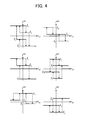
- Fig. 4 shows examples of multi-hysteresis VCCS characteristics thereof.
- the multi-screw chaotic oscillator circuit of the present invention is constituted by a linear two-port VCCS circuit 1 consisting of a set of the linear VCCS circuits G 1 and G 2 , a multi-hysteresis two-port VCCS circuit 2 consisting of a set of the multi-hysteresis VCCS circuits MH 1 and MH 2 having multi-hysteresis characteristic, and two capacitors C 1 and C 2 .
- the characteristic of the linear VCCS circuits G 1 and G 2 is as shown in Fig. 2 , wherein transconductance at the central linear sections of their input and output characteristics are identified as g m1 and g m2 , respectively.
- the multi-hysteresis VCCS circuits MH 1 and MH 2 are constituted in accordance with the method of Patent Document 1 above, for example.
- Figs. 3 and 4 show the circuit symbol and an example of the multi-hysteresis VCCS characteristic thereof, respectively.
- Fig. 5 shows an example of the normalization of the multi-hysteresis VCCS characteristic according to the present invention.
- circuit equation (3) above can be normalized as described by the following equation (12).
- equation (17) can be represented as:
- the multi-screw chaotic oscillator circuit of the present invention presents various attractors by changing the thresholds of the multi-hysteresis VCCS circuits MH 1 and MH 2 .
- the output currents of the multi-hysteresis VCCS circuits MH 1 , MH 2 take discrete values corresponding to a saturation current in each hysteresis characteristic. That is, the multi-screw chaotic oscillator circuit of the present invention is a type of hybrid system, having continuous internal state variables and corresponding discrete output variables. Then, a discrete series of the output current of the multi-hysteresis VCCS circuit on the trajectory of each attractor is taken into account as the symbol dynamics.
- the circuit exemplified here constitutes the multi-hysteresis two-port VCCS characteristic by using a set of two multi-hysteresis VCCS circuits, that is a combination of two single-hysteresis VCCS circuits.
- four discrete output states are present for each mh 1 (x( ⁇ )), mh 2 (y( ⁇ )).
- there are 4 x 4 16 combinations of these discrete output states, and corresponding 16 half spaces are present in a solution space.
- the attractors are classified based on which half space among them the solution trajectory passes through.
- a solution space S is represented using 1, m as:
- a trajectory passing half space matrix as described in this manner is denoted as B.
- the attractor represented by:
- Formula 10 B 1 0 1 1 0 1 0 0 0 0 1 0 1 1 1 indicates that the trajectory thereof passes through half spaces s 11 , s 13 , s 14 , s 22 , s 32 , s 34 , s 42 , s 43 , and s 44 .
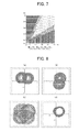
- Fig. 7 shows a two-parameter bifurcation diagram obtained therefrom.
- Fig. 7 there are 11 trajectory passing half space matrices each representing the half space through which the trajectory of each attractor passes as:
- Fig. 8 shows several examples of typical chaotic attractors in this bifurcation diagram.
- These chaotic attractors differ from those observed until now.
- the multi-screw chaotic oscillator circuit of the present invention a variety of chaotic attractors can also be obtained only by controlling the thresholds of the multi-hysteresis VCCS circuit constituting the multi-hysteresis two-port VCCS characteristic. Therefore, it is considered that changing the circuit parameters other than the thresholds allows more diverse bifurcation phenomena or chaotic attractors to be obtained.
- the chaotic attractors different from those obtained conventionally have been observed in the multi-screw chaotic oscillator circuit of the present invention.
- the bifurcation phenomena producing these chaotic attractors are very complex, and such bifurcation phenomena themselves are likely to have unique bifurcation structures.
- the fully-differential linear VCCS circuit proposed in Non-Patent Document 19 was used.
- the circuit is shown in Fig. 12 .
- the value of transconductance g m at the central linear section of input and output characteristics can be changed by changing an external control voltage V g .
- Table 1 shows the sizes of each MOSFET, used in the simulation experiment, of the fully-differential VCCS circuit.
- triangular symbols h 1 , h 2 , and h 3 represent core circuits having single-hysteresis VCCS characteristic, as shown in Fig. 14 .
- Threshold voltages of the multi-hysteresis VCCS characteristic can be changed by adjusting the external control voltages V hek of the core circuit.
- the MOSFETs having the sizes shown in Table 2 were used.
- the sizes of the MOSFETs in the core circuit shown in Fig. 14 took the values shown in Tables 3 and 4, respectively.
- the fully-differential multi-screw chaotic oscillator circuit was constituted by connecting the circuit elements described above as shown in Fig. 1 , and its chaotic attractors were observed in the SPICE simulation.
- the characteristic of the multi-hysteresis VCCS circuit MH 2 was fixed to the multi-hysteresis VCCS characteristic as shown in Fig. 15
- the hysteresis VCCS characteristic of the multi-hysteresis VCCS circuit MH 1 was changed among Fig. 16(a), (b), and (c) .
- Fig. 17 shows the chaotic attractor obtained when using the characteristic of Fig. 16(a) as the characteristic of the multi-hysteresis VCCS circuit MH 1
- Fig. 17 shows the chaotic attractor obtained when using the characteristic of Fig. 16(a) as the characteristic of the multi-hysteresis VCCS circuit MH 1
- Fig. 17 shows the chaotic attractor obtained when using the characteristic of Fig. 16(a)
- FIG. 18 shows the chaotic attractor obtained when using the characteristic of Fig. 16(b)
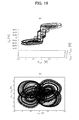
- Fig. 19 shows the chaotic attractor obtained when using the characteristic of Fig. 16(c)
- Figs. 17(a) , 18(a) , and 19(a) each shows the attractor in a phase space V od1 - (V od1 - V od2 ) - i od
- Figs. 17(b) , 18(b) , and 19(b) each shows a projection onto a plane v od1 - (v od1 - V od2 ).
- v od1 and v od2 represent differential voltages corresponding to v 1 (t) and v 2 (t) in Fig. 1 , respectively, and i od represents a differential current corresponding to i 1 (t) + i' 1 (t) in Fig. 1 .
- Table 5 shows the values of the external control voltage when these attractors were observed.
- the multi-screw chaotic oscillator circuit using the multi-hysteresis VCCS circuit. Since the multi-screw chaotic oscillator circuit does not include an inductor in spite of the fact that it is a continuous-time circuit, the circuit configuration is simpler as compared to the conventionally proposed chaotic circuits. Moreover, since a variety of multi-hysteresis VCCS characteristics can be used, various multi-screw attractors can be generated. Furthermore, by changing different characteristics of the multi-hysteresis VCCS circuit as a component, a greater number of chaotic attractors or bifurcation structures can be realized.
- the multi-screw chaotic oscillator circuit of the present invention has a number of control parameters such as the thresholds and saturation currents of the multi-hysteresis VCCS circuit, the shapes of the multi-hysteresis VCCS characteristic, and the eigenvalues of the circuit, and thus can produce the conventionally-proposed chaotic attractors as well as various chaotic attractors which have not been disclosed to date by controlling these parameters.
- the multi-screw chaotic oscillator circuit of the present invention utilizes its various high-dimensional chaotic attractors and is thus applicable to information processors using chaos.
- the multi-screw chaotic oscillator circuit of the present invention is a hybrid dynamical system, it can be utilized in the quick physical simulations of high-dimensional hybrid dynamical systems or in the information processing systems based on high-dimensional hybrid dynamics.
- the multi-screw chaotic oscillator circuit of the present invention is effective in realization of dynamic memories with a large memory capacity and multivalued logic circuits by making the discrete output states of the multi-hysteresis VCCS characteristic to be symbolic dynamics or multivalued logic values.
- various high-dimensional chaotic attractors generated by the multi-screw chaotic oscillator circuit of the present invention are useful in generation of complex spatiotemporal patterns, image processing, chaotic communications, chaotic encryption, and the like.
- the multi-screw chaotic oscillator circuit of the present invention utilizes its various high-dimensional chaotic attractors and is thus applicable to information processors using chaos.
Landscapes
- Inductance-Capacitance Distribution Constants And Capacitance-Resistance Oscillators (AREA)
- Stabilization Of Oscillater, Synchronisation, Frequency Synthesizers (AREA)
Abstract
Description
- The present invention relates to a multi-screw chaotic oscillator circuit, and particularly, to a multi-screw chaotic oscillator circuit suitable for the quick physical simulations of high-dimensional hybrid dynamical systems or for the information processing systems based on high-dimensional hybrid dynamics.
- Conventionally, the chaos generating circuits using piecewise linear single-hysteresis elements have been proposed (see Non-Patent Documents 1-13 below), and it has been reported that a variety of interesting chaotic attractors can be observed. The method has also been proposed wherein the single-hysteresis elements as components are replaced by multi-hysteresis elements that can produce multivalued outputs (see Non-Patent Documents 14-16 below). In this method, grid-scroll attractors or the like can be observed, that have not been generated in conventional chaotic circuits using single-hysteresis characteristics.
-
- Patent Document 1:
JP 2009-025790 -
- Non-Patent Document 1: R. W. Newcomb, and S. Sathyan, "An RC op amp chaos generator", IEEE Trans. on Circuits and Systems, Part I, Fundam. Theory Appl., vol. 30, no. 1, pp. 54-56, 1983
- Non-Patent Document 2: R. W. Newcomb, and N. El-Leithy, "A binary hysteresis chaos generator", in Proc. of 1984 IEEE Int'l Symp. on Circuits and Systems, pp. 856-859, 1984
- Non-Patent Document 3: Toshimichi Saito, "On a hysteresis chaos generator", in Proc. of 1985 IEEE Int'l Symp. on Circuits and Systems, pp. 847-849, 1985
- Non-Patent Document 4: Takashi Suzuki, and Toshimichi Saito, "On fundamental bifurcations from a hysteresis hyperchaos generator", IEEE Trans. on Circuits and Systems, Part I, Fundam. Theory Appl., vol. 41, no. 12, pp. 876-884, 1994
- Non-Patent Document 5: Toshimichi Saito, and Shinji Nakagawa, "Chaos from a hysteresis and switched circuit", Phil. Trans. R. Soc. Lond. A, vol. 353, no. 1701, pp. 47-57, 1995
- Non-Patent Document 6: Toshimichi Saito, and Kunihiko Mitsubori, "Control of chaos from a piecewise linear histeresis circuit", IEEE Trans. on Circuits and Systems, Part I, Fundam. Theory Appl., vol. 42, no. 3, pp. 168-172, 1995
- Non-Patent Document 7: J. E. Varrientos, and E. Sanchez-Sinencio, "A 4-D chaotic oscillator based on a differential hysteresis comparator", IEEE Trans. on Circuits and Systems, Part I, Fundam. Theory Appl., vol. 45, no. 1, pp. 3-10, 1998
- Non-Patent Document 8: A. S. Elwakil, and M. P. Kennedy, "Chaotic oscillators derived from Saito's double-screw hysteresis oscillator", IEICE Trans. Fundamentals, vol. E82-A, no. 9, pp. 1769-1775, 1999
- Non-Patent Document 9: F. Bizzarri, D. Stellardo, and M. Storace, "Bifurcation analysis and its experimental validation for a hysteresis circuit oscillator", IEEE Trans. on Circuits and Systems, Part I. Regular Papers, vol. 53, no. 7, pp. 517-521, 2006
- Non-Patent Document 10: Masaki Kataoka and Toshimichi Saito, "A 4-D chaotic oscillator with a hysteresis 2-port VCCS: The first example of chaotic oscillators consisting of 2-port VCCSs and capacitors", in Proc. IEEE Intl Symp. on Circuits and Syst., vol. 5, pp. 418-421, 1999
- Non-Patent Document 11: Masaki Kataoka and Toshimichi Saito, "A 2-port VCCS chaotic oscillator and quad screw attractor", IEEE Trans. on Circuits and Systems, Part I, Fundam. Theory Appl., vol. 48, no. 2, pp. 221-225, 2001
- Non-Patent Document 12: Masaki Katoka and Toshimichi Saito, "A chaotic oscillator based on two-port VCCS", in Chaos in Circuits and Systems, G. Chen and T. Ueda eds., pp. 131-143, World Scientific, Singapore, 2002
- Non-Patent Document 13: Kiyomitsu Ogata and Toshimichi Saito, "Chaotic attractors in a 4-D oscillator based on 2-port VCCSs", in Proc. IEEE Intl Symp. on Circuits and Syst., vol. 2, pp. 556-559, 2002
- Non-Patent Document 14: Fengling Han, Xinghuo Yu, Yuye Wang, Yong Feng, and Guanrong Chen, "n-scroll chaotic oscillators by second-order systems and double-hysteresis blocks", Electronics Letters, vol. 39, no. 23, pp. 1636-1637, 2003
- Non-Patent Document 15: Fengling Han, Xinghuo Yu, and Jiankun Hu, "A new way of generating grid-scroll chaos and its application to biometric authentication", in Proc. of IEEE 2005 Industrial Electronics Society, 31st Annual Conference, pp. 61-66, 2005
- Non-Patent Document 16: Fengling Han, Xinghuo Yu, Yong Feng, and Jiankun Hu, "On multiscroll chaotic attractors in hysteresis-based piecewise-linear systems", IEEE Trans. on Circuits and Systems, Part II, and Express Briefs, vol. 54, no. 11, pp. 1004-1008, 2007
- Non-Patent Document 17: Takuya Hamada, Yoshihiko Horio, and Kazuyuki Aihara, "An IC implementation of a hysteresis two-port VCCS chaotic oscillator", in Proc. of European Conf. on Circuits Theory and Design, pp. 926-929, 2007
- Non-Patent Document 18: Takuya Hamada, Yoshihiko Horio, and Kazuyuki Aihara, "Experimental observations from an integrated hysteresis two-port VCCS chaotic oscillator", in Proc. IEEE Int'l Work-shop on Nonlinear Dynamics of Electronic Systems, pp. 237-240, 2007
- Non-Patent Document 19: Takuya Hamada, Yoshihiko Horio, and Kazuyuki Aihara, "A Fully-Differential Hysteresis Two-Port VCCS Chaotic Oscillator", IEICE Technical Report, NLP2007-180, pp. 79-84, 2008
- However, the multi-hysteresis characteristics proposed in the above-mentioned Non-Patent Documents 14-16 only present the shapes where the single-hysteresis characteristics are combined in series, and thus chaotic attractors to be generated necessarily depend thereon. In addition, the multi-hysteresis characteristic used therein is constituted by connecting a plurality of voltage controlled voltage source circuits (VCVS circuits) having the single-hysteresis characteristics. Since inputs and outputs of such VCVS circuits are both voltages, there has been a disadvantage that connecting a plurality of circuits requires an adder, resulting in the increase in scale of the circuits.
- In view of the circumstances described above, the present invention is directed to provide a multi-screw chaotic oscillator circuit with simple configuration, that can use various multi-hysteresis VCCS characteristics and generate a variety of multi-screw attractors.
- This multi-screw chaotic oscillator circuit is intended to provide the multi-screw chaotic oscillator circuit in taking into account the chaos generating circuit using the single-hysteresis voltage controlled voltage source circuit (VCCS circuit) (Non-Patent Documents 10-13) and replacing the single-hysteresis VCCS circuit in the chaos generating circuit with the multi-hysteresis VCCS circuit.
- The multi-hysteresis VCCS circuit used herein can be realized easily with the method of realizing multi-hysteresis characteristics utilizing the feature that the VCCS circuit is a current output type (Patent Document 1) proposed by the present inventors. Moreover, since this method of realizing multi-hysteresis VCCS characteristics easily allows the utilization of a variety of multi-hysteresis characteristics, novel high-dimensional multi-screw attractors or bifurcation structures can be realized which have not been observed in Non-Patent Documents 10-13.
- In order to achieve the object described above, the present invention provides the following:
- [1] A multi-screw chaotic oscillator circuit comprising: a linear two-port VCCS circuit consisting of a set of linear VCCS circuits G1 and G2; a multi-hysteresis two-port VCCS circuit consisting of a set of multi-hysteresis VCCS circuits MH1 and MH2 having multi-hysteresis characteristic; and capacitors C1 and C2 connected to each end of a circuit configured by parallel-connecting the linear two-port VCCS circuit and the multi-hysteresis two-port VCCS circuit.
-
- [2] The multi-screw chaotic oscillator circuit according to [1] above, wherein a variety of chaotic attractors or bifurcation structures are realized by using various multi-hysteresis VCCS characteristics as the characteristics of the multi-hysteresis VCCS circuits MH1 and MH2.
-
- [3] The multi-screw chaotic oscillator circuit according to [2] above, wherein a greater number of chaotic attractors or bifurcation phenomena are presented by changing different characteristics of the multi-hysteresis VCCS circuits MH1 and MH2.
-
- [4] The multi-screw chaotic oscillator circuit according to [3] above, wherein the different characteristics of the multi-hysteresis VCCS circuits MH1 and MH2 are thresholds or saturation currents.
-
- [5] The multi-screw chaotic oscillator circuit according to [4] above, wherein the thresholds include a plurality of thresholds having different values from each other.
-
- [6] The multi-screw chaotic oscillator circuit according to [5] above, wherein the multi-hysteresis VCCS circuit MH1 has n values of the saturation current, and the multi-hysteresis VCCS circuit MH2 has m values of the saturation current.
-
- [7] The multi-screw chaotic oscillator circuit according to [6] above, wherein, when the plurality of thresholds express four values, four discrete outputs are present for each of the multi-hysteresis VCCS circuits MH1 and MH2 and 16 half spaces corresponding to the combinations of each of the four discrete outputs are present in a solution space, so that the chaotic attractors are classified based on which half space among them a solution trajectory passes through.
-
- [8] The multi-screw chaotic oscillator circuit according to [2] above, wherein a greater number of chaotic attractors or bifurcation phenomena are presented by changing a plurality of control parameters of the multi-hysteresis VCCS characteristics.
-
- [9] The multi-screw chaotic oscillator circuit according to [8] above, wherein the plurality of control parameters include the shapes of the multi-hysteresis VCCS characteristics and eigenvalues of the circuit.
-
- [10] The multi-screw chaotic oscillator circuit according to [1] above, wherein, when an attenuation parameter delta is 0.05, vibrational angular frequency parameter omega is 1.00, an equilibrium point parameter p is 0.25, and an equilibrium point parameter q is 0.25 of a normalized parameter for the multi-hysteresis two-port VCCS circuit consisting of the set of multi-hysteresis VCCS circuits MH1 and MH2 having the multi-hysteresis VCCS characteristics, the thresholds of the multi-hysteresis VCCS circuits MH1 and MH2 are changed.
-
- [11] The multi-screw chaotic oscillator circuit according to any one of [1] to [10] above, wherein capacities of the capacitors C1 and C2 are 40 pF and 10 pF, respectively.
- According to the present invention, the following effects can be achieved.
-
- (1) Since the chaotic oscillator circuit does not include an inductor in spite of the fact that it is a continuous-time circuit, a circuit with simpler configuration can be provided as compared to the conventionally-proposed chaotic circuits.
-
- (2) Since a variety of multi-hysteresis VCCS characteristics can be used, various multi-screw attractors can be generated.
-
- (3) By changing different characteristics of the multi-hysteresis VCCS circuit as a component, a greater number of chaotic attractors or bifurcation structures can be realized.
-
-
Fig. 1 shows a diagram of a multi-screw chaotic oscillator circuit of the present invention; -
Fig. 2 shows a characteristic of linear VCCS circuits G1 and G2 in the multi-screw chaotic oscillator circuit of the present invention; -
Fig. 3 shows a circuit symbol of multi-hysteresis VCCS circuits MH1 and MH2 in the multi-screw chaotic oscillator circuit of the present invention; -
Fig. 4 shows examples of multi-hysteresis VCCS characteristics of the multi-hysteresis VCCS circuit in the multi-screw chaotic oscillator circuit of the present invention; -
Fig. 5 shows examples of normalization of the multi-hysteresis VCCS characteristics according to the present invention; -
Fig. 6 shows a first example of a normalized characteristic (i = 1, 2) of two sets of multi-hysteresis VCCS circuits constituting a multi-hysteresis two-port VCCS characteristic in a configuration example of the multi-screw chaotic oscillator circuit of the present invention; -
Fig. 7 shows a two-parameter bifurcation diagram of the multi-screw chaotic oscillator circuit when thresholds Th1 (horizontal axis) and Th2 (vertical axis) of the multi-hysteresis VCCS circuit having the normalized characteristic shown inFig. 6 are used as bifurcation parameters; -
Fig. 8 shows examples of chaotic attractors of the multi-screw chaotic oscillator circuit obtained by changing the thresholds Th1 and Th2 when the normalized multi-hysteresis VCCS characteristic shown inFig. 6 is used; -
Fig. 9 shows a second example of the normalized characteristic (i = 1, 2) of two sets of multi-hysteresis VCCS circuits constituting the multi-hysteresis two-port VCCS characteristic in a configuration example of the multi-screw chaotic oscillator circuit of the present invention; -
Fig. 10 shows a two-parameter bifurcation diagram of the multi-screw chaotic oscillator circuit when the thresholds Th1 (horizontal axis) and Th2 (vertical axis) of the multi-hysteresis VCCS circuit having the normalized characteristic shown inFig. 9 are used as bifurcation parameters; -
Fig. 11 shows examples of the chaotic attractors of the multi-screw chaotic oscillator circuit obtained by changing the thresholds Th1 and Th2 when the normalized multi-hysteresis VCCS characteristic shown inFig. 9 is used; -
Fig. 12 shows a diagram of a fully-differential linear VCCS circuit used as the linear VCCS circuits G1 and G2 constituting a linear two-port VCCS circuit in the configuration example of the multi-screw chaotic oscillator circuit of the present invention; -
Fig. 13 shows a diagram of a fully-differential multi-hysteresis VCCS circuit used as the multi-hysteresis VCCS circuits MH1 and MH2 constituting the multi-hysteresis two-port VCCS circuit in the configuration example of the multi-screw chaotic oscillator circuit of the present invention; -
Fig. 14 shows a core circuit having a single-hysteresis VCCS characteristic, illustrated by the triangular symbols inFig. 13 ; -
Fig. 15 shows a characteristic of the multi-hysteresis VCCS circuit MH2 used in the SPICE simulation; -
Fig. 16 shows a characteristic of the multi-hysteresis VCCS circuit MH1 used in the SPICE simulation; -
Fig. 17 shows the chaotic attractor obtained when the characteristic shown inFig. 16(a) is used as the characteristic of the multi-hysteresis VCCS circuit MH1; -
Fig. 18 shows the chaotic attractor obtained when the characteristic shown inFig. 16(b) is used as the characteristic of the multi-hysteresis VCCS circuit MH1; and -
Fig. 19 shows the chaotic attractor obtained when the characteristic shown inFig. 16(c) is used as the characteristic of the multi-hysteresis VCCS circuit MH1. - A multi-screw chaotic oscillator circuit of the present invention comprises: a linear two-port VCCS circuit consisting of a set of linear VCCS circuits G1 and G2; a multi-hysteresis two-port VCCS circuit consisting of a set of multi-hysteresis VCCS circuits MH1 and MH2 having multi-hysteresis characteristic; and capacitors C1 and C2 connected to each end of a circuit configured by parallel-connecting the linear two-port VCCS circuit and the multi-hysteresis two-port VCCS circuit.
- Hereinafter, embodiments of the present invention will be described in detail.
-
Fig. 1 shows a diagram of a multi-screw chaotic oscillator circuit of the present invention, andFig. 2 shows a characteristic of linear VCCS circuits G1 and G2 in the multi-screw chaotic oscillator circuit, whereinFig. 2(a) shows a circuit symbol of the linear VCCS circuit, andFig. 2(b) shows its input and output characteristics.Fig. 3 shows a circuit symbol of multi-hysteresis VCCS circuits MH1 and MH2 in the multi-screw chaotic oscillator circuit of the present invention, andFig. 4 shows examples of multi-hysteresis VCCS characteristics thereof. - As shown in these figures, the multi-screw chaotic oscillator circuit of the present invention is constituted by a linear two-
port VCCS circuit 1 consisting of a set of the linear VCCS circuits G1 and G2, a multi-hysteresis two-port VCCS circuit 2 consisting of a set of the multi-hysteresis VCCS circuits MH1 and MH2 having multi-hysteresis characteristic, and two capacitors C1 and C2. - The characteristic of the linear VCCS circuits G1 and G2 is as shown in
Fig. 2 , wherein transconductance at the central linear sections of their input and output characteristics are identified as gm1 and gm2, respectively. - On the other hand, the multi-hysteresis VCCS circuits MH1 and MH2 are constituted in accordance with the method of
Patent Document 1 above, for example.Figs. 3 and4 show the circuit symbol and an example of the multi-hysteresis VCCS characteristic thereof, respectively. - Assuming voltages of the capacitors C1 and C2 as v1(t) and v2(t) and currents flowing from the capacitors C1, C2 to the linear two-
port VCCS circuit 1 inFig. 1 as i1(t), i2(t), respectively, the circuit equation of a section of the linear two-port VCCS circuit 1 is given as the following equation (1). -

port VCCS circuit 2 as i'l(t), i'2(t), respectively, the circuit equation of a section of the multi-hysteresis two-port VCCS circuit 2 inFig. 1 is given as the following equation (2). -

Fig. 4 . - The linear two-
port VCCS circuit 1 represented by the equation (1) above and the multi-hysteresis two-port VCCS circuit 2 represented by the equation (2) above connected in parallel to configure a circuit, which also has the capacitors C1, C2 connected to each end of the circuit, constitute the multi-screw chaotic oscillator circuit of the present invention as shown inFig. 1 , and the circuit equation of the overall circuit can be represented as follows. -

-


-
Fig. 5 shows an example of the normalization of the multi-hysteresis VCCS characteristic according to the present invention. - For example, the normalization of the multi-hysteresis VCCS characteristic obtained by combining two single-hysteresis VCCS characteristics H1(vd), H2(vd) shown in
Figs. 5(a) and (b) , respectively, results in a multi-hysteresis VCCS characteristic mh(x(τ)) as shown inFig. 5(c) . - By using the transformation of variables and the parameters as described above, the circuit equation (3) above can be normalized as described by the following equation (12).
-

As for p·mh1(x(τ)) and q·mh2(y(τ)) in the equation (12), the outputs of the multi-hysteresis VCCS characteristics mh1(x(τ)) and mh2(y(τ)) switch in accordance with the inputs to provide constants corresponding to each level of discrete outputs of the multi-hysteresis VCCS characteristic, so that the equation (12) above can be considered as the linear differential equation within such an interval. That is, this system can be considered as a piecewise linear system formed by combining half spaces defined by the output of the multi-hysteresis VCCS characteristic mhi(·). Therefore, by performing transformation of variables as: -

-

An eigenvalue λ of the characteristic equation (14) above is given by:
- If the parameter ν satisfies:

-

- In addition, the equation (17) can be represented as:
-

- Next, the bifurcation analysis and the attractor will be described.
- Here, there is described the possibility of the multi-screw chaotic oscillator circuit of the present invention to have diverse bifurcation phenomena and a variety of chaotic attractors through the bifurcation analysis incorporating symbolic dynamics. As an example, for simplicity, the case will be explained where each MH1 and MH2 is constituted by the multi-hysteresis VCCS circuit having a symmetrical multi-hysteresis VCCS characteristic as shown in
Fig. 5(c) that satisfies EL th1 = -ER Th1, ID 1 = -IU 1, EL th2 = -ER Th2, and ID 2 = -IU 2. Moreover, the case is discussed where, in the multi-hysteresis two-port VCCS circuit constituted by a set of these two multi-hysteresis VCCS circuits MH1 and MH2, the normalized parameters satisfy δ = 0.05, ω = 1.00, p = 0.25, and q = 0.25. At this time, the multi-screw chaotic oscillator circuit of the present invention presents various attractors by changing the thresholds of the multi-hysteresis VCCS circuits MH1 and MH2. - In order to characterize these attractors, it is noted that the output currents of the multi-hysteresis VCCS circuits MH1, MH2 take discrete values corresponding to a saturation current in each hysteresis characteristic. That is, the multi-screw chaotic oscillator circuit of the present invention is a type of hybrid system, having continuous internal state variables and corresponding discrete output variables. Then, a discrete series of the output current of the multi-hysteresis VCCS circuit on the trajectory of each attractor is taken into account as the symbol dynamics. Since the circuit exemplified here constitutes the multi-hysteresis two-port VCCS characteristic by using a set of two multi-hysteresis VCCS circuits, that is a combination of two single-hysteresis VCCS circuits, four discrete output states are present for each mh1(x(τ)), mh2(y(τ)). As such, there are 4 x 4 = 16 combinations of these discrete output states, and corresponding 16 half spaces are present in a solution space. Then, the attractors are classified based on which half space among them the solution trajectory passes through. For this purpose, four discrete output states of mh1(x(τ)) are labeled as 1, which is numbered with 1 = 1, 2, 3, 4. Similarly, the discrete output states of mh2(y(τ)) are labeled as m, which is numbered with m = 1, 2, 3, 4. Moreover, a solution space S is represented using 1, m as:
-

- Here, the attractors are classified by describing them with a binary variable, blm = "1", if the trajectory of the attractor passes through the half space slm, while describing them with blm = "0" if not. A trajectory passing half space matrix as described in this manner is denoted as B. For example, the attractor represented by:
-

- First, assuming that both of two multi-hysteresis VCCS circuits constituting the multi-hysteresis two-port VCCS characteristic have the normalized multi-hysteresis VCCS characteristic as shown in
Fig. 6 , the half space through which the solution trajectory passes was checked for the attractors obtained by changing the thresholds Th1 and Th2 of the respective circuits from 0.1 through 1.0.Fig. 7 shows a two-parameter bifurcation diagram obtained therefrom. InFig. 7 , there are 11 trajectory passing half space matrices each representing the half space through which the trajectory of each attractor passes as: -

Fig. 8 shows several examples of typical chaotic attractors in this bifurcation diagram. In this figure,Fig. 8(a) shows an example of the chaotic attractor in a domain B10 (Th1 = 0.20, Th2 = 0.60) inFig. 7, Fig. 8(b) shows an example of the chaotic attractor in a domain B5 (Th1 = 0.60, Th2 = 0.20) inFig. 7, Fig. 8(c) shows an example of the chaotic attractor in a domain B11 (Th1 = 0.20, Th2 = 0.20) inFig. 7, and Fig. 8(d) shows an example of the chaotic attractor in a domain B7 (Th1 = 0.60, Th2 = 0.60) inFig. 7 . - As the next example, assuming that both of two multi-hysteresis VCCS circuits constituting the multi-hysteresis two-port VCCS characteristic have the normalized multi-hysteresis VCCS characteristic as shown in
Fig. 9 , the half space through which the attractor passes was checked for the attractors obtained by changing the thresholds Th1 and Th2 of the respective circuits from 0.1 through 0.5.Fig. 10 shows a two-parameter bifurcation diagram obtained therefrom. In this case, since the saturation current at the central section of the normalized multi-hysteresis VCCS characteristic that was used (Fig. 9 ) is degenerated, there are three possible saturation current values of the discrete output. Therefore, the number of half space would be 3 x 3 = 9.
InFig. 10 , there are nine (3 x 3) trajectory passing half space matrices each representing the half space through which the trajectory of each attractor passes as: -


Fig. 11 shows several examples of typical chaotic attractors in this bifurcation diagram. InFig. 11, Fig. 11(a) shows an example of the chaotic attractor in a domain B1 (Th1 = 0.20, Th2 = 0.20) inFig. 10 ,Fig. 11(b) shows an example of the chaotic attractor in a domain B2 (Th1 = 0.25, Th2 = 0.25) inFig. 10 ,Fig. 11(c) shows an example of the chaotic attractor in a domain B3 (Th1 = 0.30, Th2 = 0.30) inFig. 10 ,Fig. 11 (d) shows an example of the chaotic attractor in a domain B4 (Th1 = 0.20, Th2 = 0.40) inFig. 10 ,Fig. 11(e) shows an example of the chaotic attractor in a domain B5 (Th1 = 0.20, Th2 = 0.35) inFig. 10 ,Fig. 11(f) shows an example of the chaotic attractor in a domain B6 (Th1 = 0.30, Th2 = 0.20) inFig. 10 ,Fig. 11(g) shows an example of the chaotic attractor in a domain B7 (Th1 = 0.40, Th2 = 0.20) inFig. 10 ,Fig. 11(h) shows an example of the chaotic attractor in a domain B8 (Th1 = 0.35, Th2 = 0.20) inFig. 10 , andFig. 11(i) shows an example of the chaotic attractor in a domain B9 (Th1 = 0.20, Th2 = 0.30) inFig. 10 . These chaotic attractors differ from those observed until now. - As described in the examples above, according to the multi-screw chaotic oscillator circuit of the present invention, a variety of chaotic attractors can also be obtained only by controlling the thresholds of the multi-hysteresis VCCS circuit constituting the multi-hysteresis two-port VCCS characteristic. Therefore, it is considered that changing the circuit parameters other than the thresholds allows more diverse bifurcation phenomena or chaotic attractors to be obtained. Moreover, as illustrated above, the chaotic attractors different from those obtained conventionally have been observed in the multi-screw chaotic oscillator circuit of the present invention. In addition, the bifurcation phenomena producing these chaotic attractors are very complex, and such bifurcation phenomena themselves are likely to have unique bifurcation structures.
- Next, the implementation of the multi-screw chaotic oscillator circuit will be described.
- In order to show the availability of the present invention, the fully-differential hysteresis two-port VCCS chaotic oscillator circuit of Non-Patent Documents 17-19 above was extended. The fully-differential multi-screw chaotic oscillator circuit will be described below. This circuit was designed with the TSMC 0.35 µm CMOS semiconductor process.
- As for two linear VCCS circuits G1 and G2 constituting the linear two-port VCCS circuit in the multi-screw chaotic oscillator circuit of the present invention, the fully-differential linear VCCS circuit proposed in
Non-Patent Document 19 was used. The circuit is shown inFig. 12 . In this circuit, the value of transconductance gm at the central linear section of input and output characteristics can be changed by changing an external control voltage Vg. Table 1 shows the sizes of each MOSFET, used in the simulation experiment, of the fully-differential VCCS circuit. -
[Table 1] Elements W/L Elements W/L M1,2 1µm/2µm M3,4 1.1µm/2µm M5 4.4µm/2µm M6,7 2.15µm/2µm M8,9 0.8µm/2µm M10,11 2.2µm/2µm M12,13 0.8µm/2µm Fig. 1 was implemented in accordance with the method proposed inPatent Document 1 above.Fig. 13 shows a specific circuit. InFig. 13 , triangular symbols h1, h2, and h3 represent core circuits having single-hysteresis VCCS characteristic, as shown inFig. 14 . Threshold voltages of the multi-hysteresis VCCS characteristic can be changed by adjusting the external control voltages Vhek of the core circuit. Moreover, in order to implement the multi-hysteresis VCCS circuits MH1 and MH2 in the fully-differential multi-hysteresis VCCS circuit inFig. 13 , the MOSFETs having the sizes shown in Table 2 were used. Furthermore, in order to implement the multi-hysteresis VCCS circuits MH1 and MH2, the sizes of the MOSFETs in the core circuit shown inFig. 14 took the values shown in Tables 3 and 4, respectively. -
[Table 2] Elements W/L Elements W/L M1,2,3,4,5,6 3.2µm/1.0µm M7,8,9,10,11,12 3.2µm/1.0µm M13,14,15 8.0µm/2.0µm M16,17,18 8.0µm/2.0µm M19,20,21 16.0µm/2.0µm M22,23,24 16.0µm/2.0µm M25,27 1.6µm/1.0µm M26,28 3.6µm/2.0µm M29,31 3.2µm/1.0µm M30,32 7.2µm/2.0µm M33,34,36 3.6µm/1.0µm M35 1.0µm/3.5µm -
[Table 3] Elements W/L Elements W/L M1,2 1.0µm/2.0µm M3,4 2.0µm/1.0µm M5 5.0µm/1.0µm M7 4.4µm/2.0µm M8,9 1.0µm/2.0µm M10,11 2.2µm/2.0µm M12,13 2.15µm/2.0µm M14,15 0.8µm/2.0µm -
[Table 4] Elements W/L Elements W/L M1,2 1.2µm/2.0µm M3,4 4.0µm/1.0µm N5,6 13.0µm/1.0µm M7 4.4µm/2.0µm M8,9 1.0µm/2.0µm M10,11 2.2µm/2.0µm M12,13 2.15µm/2.0µm M14,15 0.8µm/2.0µm Fig. 1 were 40 pF and 10 pF, respectively. - The fully-differential multi-screw chaotic oscillator circuit was constituted by connecting the circuit elements described above as shown in
Fig. 1 , and its chaotic attractors were observed in the SPICE simulation. In this regard, the characteristic of the multi-hysteresis VCCS circuit MH2 was fixed to the multi-hysteresis VCCS characteristic as shown inFig. 15 , while the hysteresis VCCS characteristic of the multi-hysteresis VCCS circuit MH1 was changed amongFig. 16(a), (b), and (c) .Fig. 17 shows the chaotic attractor obtained when using the characteristic ofFig. 16(a) as the characteristic of the multi-hysteresis VCCS circuit MH1,Fig. 18 shows the chaotic attractor obtained when using the characteristic ofFig. 16(b) , andFig. 19 shows the chaotic attractor obtained when using the characteristic ofFig. 16(c) . Here,Figs. 17(a) ,18(a) , and19(a) each shows the attractor in a phase space Vod1 - (Vod1 - Vod2) - iod, whileFigs. 17(b) ,18(b) , and19(b) each shows a projection onto a plane vod1 - (vod1 - Vod2). In these figures, vod1 and vod2 represent differential voltages corresponding to v1(t) and v2(t) inFig. 1 , respectively, and iod represents a differential current corresponding to i1(t) + i'1(t) inFig. 1 . Table 5 shows the values of the external control voltage when these attractors were observed. -
[Table 5] Elemental circuit Control voltage Fig. 17 Fig. 18 Fig. 19 MH1 Vhe1, Vhe2, Vhe3 1.08V 1.15V 1.17V Vref -1.25V -1.25V -1.25V Vhi 1.28V 1.40V 1.28V MH2 Vhe1 1.20V 1.20V 1.20V Vhe2 1.24V 1.24V 1.24V Vhe3 1.29V 1.29V 1.29V Vref -1.25V -1.25V -1.25V Vhi 1.27V 1.27V 1.27V G1 Vg -1.15V -1.15V -1.15V G2 Vg -1.09V -1.09V -1.09V - From the results shown in
Figs. 17 ,18 , and19 , it was verified that the circuit configuration according to the present invention can realize a variety of multi-screw attractors. - In the present invention, there is provided the multi-screw chaotic oscillator circuit using the multi-hysteresis VCCS circuit. Since the multi-screw chaotic oscillator circuit does not include an inductor in spite of the fact that it is a continuous-time circuit, the circuit configuration is simpler as compared to the conventionally proposed chaotic circuits. Moreover, since a variety of multi-hysteresis VCCS characteristics can be used, various multi-screw attractors can be generated. Furthermore, by changing different characteristics of the multi-hysteresis VCCS circuit as a component, a greater number of chaotic attractors or bifurcation structures can be realized. That is, the multi-screw chaotic oscillator circuit of the present invention has a number of control parameters such as the thresholds and saturation currents of the multi-hysteresis VCCS circuit, the shapes of the multi-hysteresis VCCS characteristic, and the eigenvalues of the circuit, and thus can produce the conventionally-proposed chaotic attractors as well as various chaotic attractors which have not been disclosed to date by controlling these parameters.
- The multi-screw chaotic oscillator circuit of the present invention utilizes its various high-dimensional chaotic attractors and is thus applicable to information processors using chaos.
- Moreover, since the multi-screw chaotic oscillator circuit of the present invention is a hybrid dynamical system, it can be utilized in the quick physical simulations of high-dimensional hybrid dynamical systems or in the information processing systems based on high-dimensional hybrid dynamics.
- In addition, the multi-screw chaotic oscillator circuit of the present invention is effective in realization of dynamic memories with a large memory capacity and multivalued logic circuits by making the discrete output states of the multi-hysteresis VCCS characteristic to be symbolic dynamics or multivalued logic values.
- Furthermore, various high-dimensional chaotic attractors generated by the multi-screw chaotic oscillator circuit of the present invention are useful in generation of complex spatiotemporal patterns, image processing, chaotic communications, chaotic encryption, and the like.
- The present invention should not be limited to the embodiments described above, and a number of variations are possible on the basis of the spirit of the present invention. These variations should not be excluded from the scope of the present invention.
- The multi-screw chaotic oscillator circuit of the present invention utilizes its various high-dimensional chaotic attractors and is thus applicable to information processors using chaos.
Claims (11)
- A multi-screw chaotic oscillator circuit comprising:(a) a linear two-port VCCS circuit consisting of a set of linear VCCS circuits G1 and G2;(b) a multi-hysteresis two-port VCCS circuit consisting of a set of multi-hysteresis VCCS circuits MH1 and MH2 having multi-hysteresis characteristic; and(c) capacitors C1 and C2 connected to each end of a circuit configured by parallel-connecting the linear two-port VCCS circuit and the multi-hysteresis two-port VCCS circuit.
- The multi-screw chaotic oscillator circuit according to claim 1, wherein a variety of chaotic attractors or bifurcation structures are realized by using various multi-hysteresis VCCS characteristics as the characteristics of the multi-hysteresis VCCS circuits MH1 and MH2.
- The multi-screw chaotic oscillator circuit according to claim 2, wherein a greater number of chaotic attractors or bifurcation phenomena are presented by changing different characteristics of the multi-hysteresis VCCS circuits MH1 and MH2.
- The multi-screw chaotic oscillator circuit according to claim 3, wherein the different characteristics of the multi-hysteresis VCCS circuits MH1 and MH2 are thresholds or saturation currents.
- The multi-screw chaotic oscillator circuit according to claim 4, wherein the thresholds include a plurality of thresholds having different values from each other.
- The multi-screw chaotic oscillator circuit according to claim 5, wherein the multi-hysteresis VCCS circuit MH1 has n values of the saturation current, and the multi-hysteresis VCCS circuit MH2 has m values of the saturation current.
- The multi-screw chaotic oscillator circuit according to claim 6, wherein, when the plurality of thresholds express four values, four discrete outputs are present for each of the multi-hysteresis VCCS circuits MH1 and MH2 and 16 half spaces corresponding to the combinations of each of the four discrete outputs are present in a solution space, so that the chaotic attractors are classified based on which half space among them a solution trajectory passes through.
- The multi-screw chaotic oscillator circuit according to claim 2, wherein a greater number of chaotic attractors or bifurcation phenomena are presented by changing a plurality of control parameters of the multi-hysteresis VCCS characteristics.
- The multi-screw chaotic oscillator circuit according to claim 8, wherein the plurality of control parameters include the shapes of the multi-hysteresis VCCS characteristics and eigenvalues of the circuit.
- The multi-screw chaotic oscillator circuit according to claim 1, wherein, when an attenuation parameter delta is 0.05, vibrational angular frequency parameter omega is 1.00, an equilibrium point parameter p is 0.25, and an equilibrium point parameter q is 0.25 of a normalized parameter for the multi-hysteresis two-port VCCS circuit consisting of the set of multi-hysteresis VCCS circuits MH1 and MH2 having the multi-hysteresis VCCS characteristics, the thresholds of the multi-hysteresis VCCS circuits MH1 and MH2 are changed.
- The multi-screw chaotic oscillator circuit according to any one of claims 1 to 10, wherein capacities of the capacitors C1 and C2 are 40 pF and 10 pF, respectively.
Applications Claiming Priority (2)
| Application Number | Priority Date | Filing Date | Title |
|---|---|---|---|
| JP2009071195 | 2009-03-24 | ||
| PCT/JP2010/001687 WO2010109793A1 (en) | 2009-03-24 | 2010-03-10 | Multi-screw chaotic oscillator circuit |
Publications (3)
| Publication Number | Publication Date |
|---|---|
| EP2413501A1 true EP2413501A1 (en) | 2012-02-01 |
| EP2413501A4 EP2413501A4 (en) | 2012-10-17 |
| EP2413501B1 EP2413501B1 (en) | 2018-01-03 |
Family
ID=42780492
Family Applications (1)
| Application Number | Title | Priority Date | Filing Date |
|---|---|---|---|
| EP10755597.1A Not-in-force EP2413501B1 (en) | 2009-03-24 | 2010-03-10 | Multi-screw chaotic oscillator circuit |
Country Status (4)
| Country | Link |
|---|---|
| US (1) | US8766732B2 (en) |
| EP (1) | EP2413501B1 (en) |
| JP (1) | JP5158823B2 (en) |
| WO (1) | WO2010109793A1 (en) |
Families Citing this family (3)
| Publication number | Priority date | Publication date | Assignee | Title |
|---|---|---|---|---|
| US8823464B2 (en) * | 2011-11-01 | 2014-09-02 | Instituto Potosino de Investigacion Cientifica y Tecnológica A.C. | Reconfigurable multivibrator element based on chaos control |
| CN104868888B (en) * | 2015-05-25 | 2017-12-26 | 兰州大学 | A kind of hysteresis loop comparator of multi output state |
| CN107623567B (en) * | 2017-09-30 | 2020-10-16 | 湖南科技大学 | Chaotic circuit with constant Lyapunov exponent spectra |
Family Cites Families (1)
| Publication number | Priority date | Publication date | Assignee | Title |
|---|---|---|---|---|
| JP5106194B2 (en) | 2007-06-19 | 2012-12-26 | 株式会社リコー | Electrophotographic photoreceptor, manufacturing method, image forming method using the same, image forming apparatus, and process cartridge for image forming apparatus |
-
2010
- 2010-03-10 JP JP2011505845A patent/JP5158823B2/en not_active Expired - Fee Related
- 2010-03-10 WO PCT/JP2010/001687 patent/WO2010109793A1/en not_active Ceased
- 2010-03-10 EP EP10755597.1A patent/EP2413501B1/en not_active Not-in-force
- 2010-03-10 US US13/259,553 patent/US8766732B2/en not_active Expired - Fee Related
Non-Patent Citations (4)
| Title |
|---|
| BIZZARRI F ET AL: "RC op-amp implementation of hysteresis chaotic oscillator", ELECTRONICS LETTERS, IEE STEVENAGE, GB, vol. 37, no. 4, 15 February 2001 (2001-02-15), pages 209-211, XP006016269, ISSN: 0013-5194, DOI: 10.1049/EL:20010148 * |
| JOSEPH E VARRIENTOS ET AL: "A 4-D Chaotic Oscillator Based on a Differential Hysteresis Comparator", IEEE TRANSACTIONS ON CIRCUITS AND SYSTEMS PART I: REGULAR PAPERS, IEEE SERVICE CENTER, NEW YORK, NY, US, vol. 45, no. 1, 1 January 1998 (1998-01-01), XP011011679, ISSN: 1057-7122 * |
| OGATA K ET AL: "COEXISTING CHAOTIC ATTRACTORS IN AN OSCILLATOR WITH 2-PORT HYSTERESIS VCCS", IEICE TRANSACTIONS ON FUNDAMENTALS OF ELECTRONICS,COMMUNICATIONS AND COMPUTER SCIENCES, ENGINEERING SCIENCES SOCIETY, TOKYO, JP, vol. E86A, no. 6, 1 June 2003 (2003-06-01) , pages 1550-1553, XP001171100, ISSN: 0916-8508 * |
| See also references of WO2010109793A1 * |
Also Published As
| Publication number | Publication date |
|---|---|
| US20120019330A1 (en) | 2012-01-26 |
| WO2010109793A1 (en) | 2010-09-30 |
| EP2413501A4 (en) | 2012-10-17 |
| EP2413501B1 (en) | 2018-01-03 |
| JPWO2010109793A1 (en) | 2012-09-27 |
| US8766732B2 (en) | 2014-07-01 |
| JP5158823B2 (en) | 2013-03-06 |
Similar Documents
| Publication | Publication Date | Title |
|---|---|---|
| Bao et al. | Self-excited and hidden attractors found simultaneously in a modified Chua's circuit | |
| EP2413501B1 (en) | Multi-screw chaotic oscillator circuit | |
| Volos et al. | A dream that has come true: Chaos from a nonlinear circuit with a real memristor | |
| Nazarimehr et al. | Investigating chaotic attractor of the simplest chaotic system with a line of equilibria | |
| Xie et al. | Generating different types of multi-double-scroll and multi-double-wing hidden attractors | |
| Srinivasan et al. | Duffing–van der Pol oscillator type dynamics in Murali–Lakshmanan–Chua (MLC) circuit | |
| Tsubone et al. | Manifold piecewise constant systems and chaos | |
| Laskaridis et al. | Study of a chaotic circuit with a physical memristor as a nonlinear resistor | |
| Elwakil | Nonautonomous pulse-driven chaotic oscillator based on Chua's circuit | |
| Pisarchik et al. | Homoclinic orbits in a piecewise linear Rössler-like circuit | |
| EP2395663B1 (en) | Multi-hysteresis voltage controlled current source system | |
| Shukla et al. | Computing with coupled relaxation oscillators | |
| Miyachi et al. | Response of a simple dependent switched capacitor circuit to a pulse-train input | |
| Núñez et al. | Insights into the dynamics of coupled VO 2 oscillators for ONNs | |
| Murali et al. | Controlling of chaos in the driven Chua's circuit | |
| Fouda et al. | Power dissipation of memristor-based relaxation oscillators | |
| Hishiki et al. | Bifurcation analysis of a resonate-and-fire-type digital spiking neuron | |
| Wang | Interactions between neural networks: a mechanism for tuning chaos and oscillations | |
| Manimehan et al. | Enriched dynamics of a simple nonlinear nonautonomous parallel LCR circuit | |
| Kareem et al. | Study of the dynamic properties of chaotic circuits in the presence of memristors | |
| Shimazaki et al. | Synchronization and window map from pulse-coupled relaxation oscillators | |
| Ogata et al. | Chaotic attractors in a 4-D oscillator based on 2-port VCCSs | |
| Sivaganesh et al. | Emergence of dynamical hysteresis in a second-order non-autonomous chaotic circuit | |
| Priyanka Kumari et al. | Design and Implementation of Efficient MOSFET’s Utilization Based Proposed Voltage Controlled Oscillator | |
| He et al. | Stability of switched nonlinear systems under persistent dwell-time constraints |
Legal Events
| Date | Code | Title | Description |
|---|---|---|---|
| PUAI | Public reference made under article 153(3) epc to a published international application that has entered the european phase |
Free format text: ORIGINAL CODE: 0009012 |
|
| 17P | Request for examination filed |
Effective date: 20110921 |
|
| AK | Designated contracting states |
Kind code of ref document: A1 Designated state(s): AT BE BG CH CY CZ DE DK EE ES FI FR GB GR HR HU IE IS IT LI LT LU LV MC MK MT NL NO PL PT RO SE SI SK SM TR |
|
| DAX | Request for extension of the european patent (deleted) | ||
| A4 | Supplementary search report drawn up and despatched |
Effective date: 20120914 |
|
| RIC1 | Information provided on ipc code assigned before grant |
Ipc: H03K 3/0231 20060101ALI20120910BHEP Ipc: H03K 3/84 20060101ALI20120910BHEP Ipc: H03K 3/354 20060101AFI20120910BHEP |
|
| 17Q | First examination report despatched |
Effective date: 20130417 |
|
| GRAP | Despatch of communication of intention to grant a patent |
Free format text: ORIGINAL CODE: EPIDOSNIGR1 |
|
| INTG | Intention to grant announced |
Effective date: 20171010 |
|
| GRAS | Grant fee paid |
Free format text: ORIGINAL CODE: EPIDOSNIGR3 |
|
| GRAA | (expected) grant |
Free format text: ORIGINAL CODE: 0009210 |
|
| AK | Designated contracting states |
Kind code of ref document: B1 Designated state(s): AT BE BG CH CY CZ DE DK EE ES FI FR GB GR HR HU IE IS IT LI LT LU LV MC MK MT NL NO PL PT RO SE SI SK SM TR |
|
| REG | Reference to a national code |
Ref country code: GB Ref legal event code: FG4D |
|
| REG | Reference to a national code |
Ref country code: CH Ref legal event code: EP Ref country code: AT Ref legal event code: REF Ref document number: 961143 Country of ref document: AT Kind code of ref document: T Effective date: 20180115 |
|
| REG | Reference to a national code |
Ref country code: IE Ref legal event code: FG4D |
|
| REG | Reference to a national code |
Ref country code: DE Ref legal event code: R096 Ref document number: 602010047792 Country of ref document: DE |
|
| REG | Reference to a national code |
Ref country code: FR Ref legal event code: PLFP Year of fee payment: 9 |
|
| REG | Reference to a national code |
Ref country code: NL Ref legal event code: MP Effective date: 20180103 |
|
| REG | Reference to a national code |
Ref country code: LT Ref legal event code: MG4D |
|
| REG | Reference to a national code |
Ref country code: AT Ref legal event code: MK05 Ref document number: 961143 Country of ref document: AT Kind code of ref document: T Effective date: 20180103 |
|
| PG25 | Lapsed in a contracting state [announced via postgrant information from national office to epo] |
Ref country code: NL Free format text: LAPSE BECAUSE OF FAILURE TO SUBMIT A TRANSLATION OF THE DESCRIPTION OR TO PAY THE FEE WITHIN THE PRESCRIBED TIME-LIMIT Effective date: 20180103 |
|
| PG25 | Lapsed in a contracting state [announced via postgrant information from national office to epo] |
Ref country code: ES Free format text: LAPSE BECAUSE OF FAILURE TO SUBMIT A TRANSLATION OF THE DESCRIPTION OR TO PAY THE FEE WITHIN THE PRESCRIBED TIME-LIMIT Effective date: 20180103 Ref country code: CY Free format text: LAPSE BECAUSE OF FAILURE TO SUBMIT A TRANSLATION OF THE DESCRIPTION OR TO PAY THE FEE WITHIN THE PRESCRIBED TIME-LIMIT Effective date: 20180103 Ref country code: LT Free format text: LAPSE BECAUSE OF FAILURE TO SUBMIT A TRANSLATION OF THE DESCRIPTION OR TO PAY THE FEE WITHIN THE PRESCRIBED TIME-LIMIT Effective date: 20180103 Ref country code: FI Free format text: LAPSE BECAUSE OF FAILURE TO SUBMIT A TRANSLATION OF THE DESCRIPTION OR TO PAY THE FEE WITHIN THE PRESCRIBED TIME-LIMIT Effective date: 20180103 Ref country code: NO Free format text: LAPSE BECAUSE OF FAILURE TO SUBMIT A TRANSLATION OF THE DESCRIPTION OR TO PAY THE FEE WITHIN THE PRESCRIBED TIME-LIMIT Effective date: 20180403 Ref country code: HR Free format text: LAPSE BECAUSE OF FAILURE TO SUBMIT A TRANSLATION OF THE DESCRIPTION OR TO PAY THE FEE WITHIN THE PRESCRIBED TIME-LIMIT Effective date: 20180103 |
|
| PG25 | Lapsed in a contracting state [announced via postgrant information from national office to epo] |
Ref country code: IS Free format text: LAPSE BECAUSE OF FAILURE TO SUBMIT A TRANSLATION OF THE DESCRIPTION OR TO PAY THE FEE WITHIN THE PRESCRIBED TIME-LIMIT Effective date: 20180503 Ref country code: BG Free format text: LAPSE BECAUSE OF FAILURE TO SUBMIT A TRANSLATION OF THE DESCRIPTION OR TO PAY THE FEE WITHIN THE PRESCRIBED TIME-LIMIT Effective date: 20180403 Ref country code: AT Free format text: LAPSE BECAUSE OF FAILURE TO SUBMIT A TRANSLATION OF THE DESCRIPTION OR TO PAY THE FEE WITHIN THE PRESCRIBED TIME-LIMIT Effective date: 20180103 Ref country code: LV Free format text: LAPSE BECAUSE OF FAILURE TO SUBMIT A TRANSLATION OF THE DESCRIPTION OR TO PAY THE FEE WITHIN THE PRESCRIBED TIME-LIMIT Effective date: 20180103 Ref country code: SE Free format text: LAPSE BECAUSE OF FAILURE TO SUBMIT A TRANSLATION OF THE DESCRIPTION OR TO PAY THE FEE WITHIN THE PRESCRIBED TIME-LIMIT Effective date: 20180103 Ref country code: GR Free format text: LAPSE BECAUSE OF FAILURE TO SUBMIT A TRANSLATION OF THE DESCRIPTION OR TO PAY THE FEE WITHIN THE PRESCRIBED TIME-LIMIT Effective date: 20180404 Ref country code: PL Free format text: LAPSE BECAUSE OF FAILURE TO SUBMIT A TRANSLATION OF THE DESCRIPTION OR TO PAY THE FEE WITHIN THE PRESCRIBED TIME-LIMIT Effective date: 20180103 |
|
| REG | Reference to a national code |
Ref country code: DE Ref legal event code: R097 Ref document number: 602010047792 Country of ref document: DE |
|
| PG25 | Lapsed in a contracting state [announced via postgrant information from national office to epo] |
Ref country code: IT Free format text: LAPSE BECAUSE OF FAILURE TO SUBMIT A TRANSLATION OF THE DESCRIPTION OR TO PAY THE FEE WITHIN THE PRESCRIBED TIME-LIMIT Effective date: 20180103 Ref country code: EE Free format text: LAPSE BECAUSE OF FAILURE TO SUBMIT A TRANSLATION OF THE DESCRIPTION OR TO PAY THE FEE WITHIN THE PRESCRIBED TIME-LIMIT Effective date: 20180103 Ref country code: RO Free format text: LAPSE BECAUSE OF FAILURE TO SUBMIT A TRANSLATION OF THE DESCRIPTION OR TO PAY THE FEE WITHIN THE PRESCRIBED TIME-LIMIT Effective date: 20180103 |
|
| REG | Reference to a national code |
Ref country code: CH Ref legal event code: PL |
|
| PLBE | No opposition filed within time limit |
Free format text: ORIGINAL CODE: 0009261 |
|
| STAA | Information on the status of an ep patent application or granted ep patent |
Free format text: STATUS: NO OPPOSITION FILED WITHIN TIME LIMIT |
|
| PG25 | Lapsed in a contracting state [announced via postgrant information from national office to epo] |
Ref country code: MC Free format text: LAPSE BECAUSE OF FAILURE TO SUBMIT A TRANSLATION OF THE DESCRIPTION OR TO PAY THE FEE WITHIN THE PRESCRIBED TIME-LIMIT Effective date: 20180103 Ref country code: SM Free format text: LAPSE BECAUSE OF FAILURE TO SUBMIT A TRANSLATION OF THE DESCRIPTION OR TO PAY THE FEE WITHIN THE PRESCRIBED TIME-LIMIT Effective date: 20180103 Ref country code: DK Free format text: LAPSE BECAUSE OF FAILURE TO SUBMIT A TRANSLATION OF THE DESCRIPTION OR TO PAY THE FEE WITHIN THE PRESCRIBED TIME-LIMIT Effective date: 20180103 Ref country code: SK Free format text: LAPSE BECAUSE OF FAILURE TO SUBMIT A TRANSLATION OF THE DESCRIPTION OR TO PAY THE FEE WITHIN THE PRESCRIBED TIME-LIMIT Effective date: 20180103 Ref country code: CZ Free format text: LAPSE BECAUSE OF FAILURE TO SUBMIT A TRANSLATION OF THE DESCRIPTION OR TO PAY THE FEE WITHIN THE PRESCRIBED TIME-LIMIT Effective date: 20180103 |
|
| REG | Reference to a national code |
Ref country code: BE Ref legal event code: MM Effective date: 20180331 |
|
| 26N | No opposition filed |
Effective date: 20181005 |
|
| REG | Reference to a national code |
Ref country code: IE Ref legal event code: MM4A |
|
| PG25 | Lapsed in a contracting state [announced via postgrant information from national office to epo] |
Ref country code: LU Free format text: LAPSE BECAUSE OF NON-PAYMENT OF DUE FEES Effective date: 20180310 |
|
| PG25 | Lapsed in a contracting state [announced via postgrant information from national office to epo] |
Ref country code: IE Free format text: LAPSE BECAUSE OF NON-PAYMENT OF DUE FEES Effective date: 20180310 |
|
| PG25 | Lapsed in a contracting state [announced via postgrant information from national office to epo] |
Ref country code: CH Free format text: LAPSE BECAUSE OF NON-PAYMENT OF DUE FEES Effective date: 20180331 Ref country code: LI Free format text: LAPSE BECAUSE OF NON-PAYMENT OF DUE FEES Effective date: 20180331 Ref country code: SI Free format text: LAPSE BECAUSE OF FAILURE TO SUBMIT A TRANSLATION OF THE DESCRIPTION OR TO PAY THE FEE WITHIN THE PRESCRIBED TIME-LIMIT Effective date: 20180103 Ref country code: BE Free format text: LAPSE BECAUSE OF NON-PAYMENT OF DUE FEES Effective date: 20180331 |
|
| PGFP | Annual fee paid to national office [announced via postgrant information from national office to epo] |
Ref country code: GB Payment date: 20190320 Year of fee payment: 10 Ref country code: DE Payment date: 20190321 Year of fee payment: 10 Ref country code: FR Payment date: 20190322 Year of fee payment: 10 |
|
| PG25 | Lapsed in a contracting state [announced via postgrant information from national office to epo] |
Ref country code: MT Free format text: LAPSE BECAUSE OF NON-PAYMENT OF DUE FEES Effective date: 20180310 |
|
| PG25 | Lapsed in a contracting state [announced via postgrant information from national office to epo] |
Ref country code: TR Free format text: LAPSE BECAUSE OF FAILURE TO SUBMIT A TRANSLATION OF THE DESCRIPTION OR TO PAY THE FEE WITHIN THE PRESCRIBED TIME-LIMIT Effective date: 20180103 |
|
| PG25 | Lapsed in a contracting state [announced via postgrant information from national office to epo] |
Ref country code: PT Free format text: LAPSE BECAUSE OF FAILURE TO SUBMIT A TRANSLATION OF THE DESCRIPTION OR TO PAY THE FEE WITHIN THE PRESCRIBED TIME-LIMIT Effective date: 20180103 Ref country code: HU Free format text: LAPSE BECAUSE OF FAILURE TO SUBMIT A TRANSLATION OF THE DESCRIPTION OR TO PAY THE FEE WITHIN THE PRESCRIBED TIME-LIMIT; INVALID AB INITIO Effective date: 20100310 |
|
| PG25 | Lapsed in a contracting state [announced via postgrant information from national office to epo] |
Ref country code: MK Free format text: LAPSE BECAUSE OF NON-PAYMENT OF DUE FEES Effective date: 20180103 |
|
| REG | Reference to a national code |
Ref country code: DE Ref legal event code: R119 Ref document number: 602010047792 Country of ref document: DE |
|
| PG25 | Lapsed in a contracting state [announced via postgrant information from national office to epo] |
Ref country code: DE Free format text: LAPSE BECAUSE OF NON-PAYMENT OF DUE FEES Effective date: 20201001 Ref country code: FR Free format text: LAPSE BECAUSE OF NON-PAYMENT OF DUE FEES Effective date: 20200331 |
|
| GBPC | Gb: european patent ceased through non-payment of renewal fee |
Effective date: 20200310 |
|
| PG25 | Lapsed in a contracting state [announced via postgrant information from national office to epo] |
Ref country code: GB Free format text: LAPSE BECAUSE OF NON-PAYMENT OF DUE FEES Effective date: 20200310 |