EP2413486A1 - Dc power supply device - Google Patents
Dc power supply device Download PDFInfo
- Publication number
- EP2413486A1 EP2413486A1 EP10755623A EP10755623A EP2413486A1 EP 2413486 A1 EP2413486 A1 EP 2413486A1 EP 10755623 A EP10755623 A EP 10755623A EP 10755623 A EP10755623 A EP 10755623A EP 2413486 A1 EP2413486 A1 EP 2413486A1
- Authority
- EP
- European Patent Office
- Prior art keywords
- switch element
- current
- timing
- reactor
- period
- Prior art date
- Legal status (The legal status is an assumption and is not a legal conclusion. Google has not performed a legal analysis and makes no representation as to the accuracy of the status listed.)
- Withdrawn
Links
- 238000009499 grossing Methods 0.000 claims description 3
- 230000008859 change Effects 0.000 description 3
- 230000008901 benefit Effects 0.000 description 2
- 230000003247 decreasing effect Effects 0.000 description 2
- 230000001939 inductive effect Effects 0.000 description 2
- 238000001514 detection method Methods 0.000 description 1
- 238000010586 diagram Methods 0.000 description 1
- 238000001914 filtration Methods 0.000 description 1
- 230000007774 longterm Effects 0.000 description 1
- 238000000034 method Methods 0.000 description 1
- 230000004048 modification Effects 0.000 description 1
- 238000012986 modification Methods 0.000 description 1
- 230000002265 prevention Effects 0.000 description 1
- 230000008569 process Effects 0.000 description 1
- 230000009467 reduction Effects 0.000 description 1
- 238000005070 sampling Methods 0.000 description 1
- 230000001360 synchronised effect Effects 0.000 description 1
Images



Classifications
-
- H—ELECTRICITY
- H02—GENERATION; CONVERSION OR DISTRIBUTION OF ELECTRIC POWER
- H02M—APPARATUS FOR CONVERSION BETWEEN AC AND AC, BETWEEN AC AND DC, OR BETWEEN DC AND DC, AND FOR USE WITH MAINS OR SIMILAR POWER SUPPLY SYSTEMS; CONVERSION OF DC OR AC INPUT POWER INTO SURGE OUTPUT POWER; CONTROL OR REGULATION THEREOF
- H02M1/00—Details of apparatus for conversion
- H02M1/14—Arrangements for reducing ripples from DC input or output
- H02M1/15—Arrangements for reducing ripples from DC input or output using active elements
-
- H—ELECTRICITY
- H02—GENERATION; CONVERSION OR DISTRIBUTION OF ELECTRIC POWER
- H02M—APPARATUS FOR CONVERSION BETWEEN AC AND AC, BETWEEN AC AND DC, OR BETWEEN DC AND DC, AND FOR USE WITH MAINS OR SIMILAR POWER SUPPLY SYSTEMS; CONVERSION OF DC OR AC INPUT POWER INTO SURGE OUTPUT POWER; CONTROL OR REGULATION THEREOF
- H02M1/00—Details of apparatus for conversion
- H02M1/42—Circuits or arrangements for compensating for or adjusting power factor in converters or inverters
- H02M1/4208—Arrangements for improving power factor of AC input
- H02M1/4225—Arrangements for improving power factor of AC input using a non-isolated boost converter
-
- Y—GENERAL TAGGING OF NEW TECHNOLOGICAL DEVELOPMENTS; GENERAL TAGGING OF CROSS-SECTIONAL TECHNOLOGIES SPANNING OVER SEVERAL SECTIONS OF THE IPC; TECHNICAL SUBJECTS COVERED BY FORMER USPC CROSS-REFERENCE ART COLLECTIONS [XRACs] AND DIGESTS
- Y02—TECHNOLOGIES OR APPLICATIONS FOR MITIGATION OR ADAPTATION AGAINST CLIMATE CHANGE
- Y02B—CLIMATE CHANGE MITIGATION TECHNOLOGIES RELATED TO BUILDINGS, e.g. HOUSING, HOUSE APPLIANCES OR RELATED END-USER APPLICATIONS
- Y02B70/00—Technologies for an efficient end-user side electric power management and consumption
- Y02B70/10—Technologies improving the efficiency by using switched-mode power supplies [SMPS], i.e. efficient power electronics conversion e.g. power factor correction or reduction of losses in power supplies or efficient standby modes
Definitions
- the present invention relates to a DC power supply device of a reactor-input type, and more specifically, to a DC power supply device capable of properly setting timing to operate a switch element that short-circuits the output of a reactor, regardless of specifications of AC power or the like.
- a DC power supply device of a reactor-input type is formed chiefly of a rectifier 1 that full-wave rectifies AC power, a reactor 2 that is an inductive element connected to one of the output terminals of the rectifier 1, and a condenser 3 that smoothes output from the reactor 2 and supplies the output to load RL, basically as shown in FIG. 1 .
- Patent Document 1 Japanese Patent No. 2763479
- the switch element 5 short-circuits the output of the reactor 2 and thus approximates a current waveform to a sine wave, which is delivered from the reactor 2 through the diode 4 to the condenser 3, thereby preventing harmonic generation. Whether or not the current waveform can successfully approximate to the sine wave, however, depends greatly upon the turn-on/off timing of the switch element 5. On top of that, the best turn-on/off timing of the switch element 5 varies according to the specifications (voltage, frequency) of an alternator, load status, etc.
- the present invention has been made in light of the above circumstances. It is an object of the invention to provide a DC power supply device capable of preventing harmonic generation by properly setting the turn-on/off timing of a switch element that short-circuits the output of a reactor, regardless of specifications of AC power, load status, etc.
- a DC power supply device of the invention is designed to effectively prevent harmonic generation, regardless of specifications of AC power, load status, etc., by setting proper timing for turning on/off the switch element through arithmetic processing based upon a time period in which no current flows.
- the DC power supply device of the invention is characterized by having means for entering electric power that is full-wave rectified by a rectifier into a rector and supplying load with output current from the reactor after directing the current to a condenser through a backflow preventing diode for smoothing the current, and a switch element that short-circuits the output of the reactor in sync with a cycle of the full-wave rectified electric power and thus prevents harmonic generation, the device being characterized in that switch control means that includes current-detecting means for sequentially detecting the current delivered from the reactor and performs turn-on/off control of the switch element has first means that determines a first OFF period in which the output current from the reactor is zero in an initial stage of the cycle from turn-on timing of the switch element and determines a second OFF period in which the output current from the reactor is zero in a late stage of the cycle from timing at which the current delivered from the reactor becomes zero after the switch element is turned off; and second means that reactivates the first means after modifying the turn
- the target OFF period is determined, for example, by multiplying the second OFF period by a predetermined coefficient.
- the switch control means is designed to control the turn-on/off timing of the switch element, using as a start point the timing for detecting a zero-crossing point of AC voltage in an alternator, which is entered into the rectifier.
- the turn-off timing of the switch element is set, for example, as timing at which the current delivered from the reactor exceeds a preset current threshold value.
- the current threshold value is evaluated as a current waveform (sine wave) obtained by multiplying a target current waveform (sine wave) for one duty cycle by a predetermined coefficient, which is evaluated to be equivalent to the amount of current delivered from the reactor to the load during the one duty cycle. It is also possible to set the turn-off timing of the switch element by adjusting DC voltage supplied to the load equals to preset target DC voltage.
- the turn-on timing of the switch element can be properly set by predetermined arithmetic processing on the basis of a period in which the current delivered from the reactor, especially, the current supplied through the diode to the condenser, is zero.
- the turn-off timing of the switch element can also be properly set on the basis of the current short-circuited by the switch element.
- the turn-on/off timing of the switch element can be properly and easily set according to specifications of an alternator, use conditions of the DC power supply device, etc. Harmonic generation can be prevented with efficiency, regardless of the specifications of the alternator, load status, etc.
- the turn-on/off timing of the switch element is beforehand normally set, the turn-on/off timing of the switch element is modified by degree according to the current delivered from the reactor on the basis of the use conditions of the device, and is thus made proper. Consequently, harmonic generation can be effectively prevented according to various kinds of usage environment.
- This DC power supply device is of a so-called reactor-input type. Basically, the device is formed chiefly of a rectifier 1 that full-wave rectifies AC power as shown in FIG. 1 , a reactor 2 that is an inductive element whose first end is connected to a plus output terminal of the rectifier 1, and a condenser 3 that is connected between a second end of the reactor 2 and a minus output terminal of the rectifier 1 and supplies an output current from the reactor 2 to load RL after smoothing the current.
- a backflow preventing diode 4 is serially interposed between the second end of the reactor 2 and the condenser 3.
- the switch element 5 Connected between the second end of the reactor 2 and the minus output terminal of the rectifier 1 is a switch element 5 that short-circuits the reactor 2 and discontinues current supply to the load side.
- the switch element 5 is made up of an IGBT and a MOS transistor which are turned on/off (ON-OFF controlled) by a switch controller (switch controlling means) 6.
- the switch controller 6 functions to turn on/off the switch element 5 at predetermined timing, basically using as synchronization reference timing a zero-crossing point of the alternator, which is detected by a zero-crossing detector 7.
- the switch controller 6 installed in a conventional DC power supply device fixes turn-on/off timing of the switch element 5 according to the specifications of a power supply or selects one of prepared patterns of turn-on/off timing according to load specification and the use conditions of the power supply device.
- a shunt resistance 8 is serially placed on the minus output terminal side of the rectifier 1.
- the switch controller 6 properly sets turn-on timing Ton and turn-off timing Toff of the switch element 5 as mentioned later on the basis of output current of the reactor 2, which is detected by the shunt resistance 8.
- Current I detected by the shunt resistance 8 is the output current from the reactor 2 short-circuited by the switch element 5 when the switch element 5 is in the ON position.
- the current I is the current supplied from the reactor 2 through the diode 4 to the condenser 3 and thus to the load RL side.
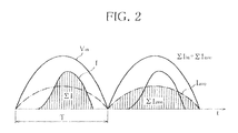
- Input voltage Vin that is full-wave rectified by the rectifier 1 and entered into the reactor 2 is, as shown in FIG. 2 , a half-cycle sine wave (plus component) whose reference point is a zero-crossing point of the alternator.
- a cycle T of the half-cycle sine wave is half of a cycle of an AC voltage waveform.
- the input current Iin that flows in through the reactor 2 starts flowing from a time point Ton at which the switch element 5 is turned on and is gradually increased as shown in FIG. 3 .
- the input current Iin flows in through the diode 4 to charge the condenser 3 from a time point Toff at which the switch element 5 is turned off.
- the switch element 5 is in the ON position (ON period,)
- the input current Iin is all short-circuited by the switch element 5, and is not supplied to the condenser 3 (load RL side) through the diode 4.
- harmonic generation can be prevented.
- the turn-off timing Toff of the switch element 5 is set in consideration of average current Iave flowing during the cycle T of the current I delivered from the reactor 2, and the turn-on timing Ton of the switch element 5 is properly set on the basis of timing at which the current I becomes zero after the switch element 5 is turned off.
- the average input current Iave flowing during the cycle T of the current I delivered from the reactor 2 is defined as current (half-cycle sine wave) in which a current amount ⁇ I that is an integrated value of the output current I from the reactor 2 within the cycle T as shown in FIG. 2 is averagely entered into the reactor 2 according to the input voltage Vin.
- a current amount ⁇ Iave of the current Iave is determined to be equal to the current amount ⁇ I.
- the present embodiment sets as the turn-off timing Toff of the switch element 5 the timing at which the current I delivered from the reactor 2 by the turn-on of the switch element 5 exceeds threshold current Ith shown in FIG. 3 , which is evaluated by multiplying the average current Iave by a predetermined coefficient ⁇ (>1.) .
- the turn-on of the switch element 5 causes the current I to be delivered from the reactor 2, and the output current I is increased by degree.
- the turn-off timing of the switch element 5 is set according to the magnitude of the current I delivered from the reactor 2.
- a first OFF period TI in which the input current Iin is maintained at zero in an initial stage of the cycle T is determined from the turn-on timing Ton of the switch element 5, which is temporarily set.
- a second OFF period T2 in which the input current Iin becomes zero in a late stage of the cycle T is determined from timing Tend at which the input current Iin (current supplied through the diode 4 to the condenser 3) becomes zero after the switch element 5 is turned off [first means].
- a target OFF period T3 in the initial stage is determined on the basis of the second OFF period T2 determined as described above, and the first OFF period Tl, or more specifically, the turn-on timing Ton of the switch element 5, is changed so as to approximate to the target OFF period T3 [second means].
- the timing at which the current I delivered from the reactor 2 exceeds the threshold current Ith is changed.
- the turn-off timing Toff of the switch element 5 is accordingly changed. This consequently changes the timing Tend at which the current (output current I) that is supplied from the reactor 2 through the diode 4 to the condenser 3 after the switch element 5 is turned off, thereby changing the second OFF period T2.
- the processing in the first means is carried out again [second means], and the second OFF period T2 is newly determined, to thereby set a new target OFF period T3. If the processing is repeatedly carried out, the first OFF period T1 gradually converges at the target OFF period T3 that is newly determined, which optimizes the turn-on timing Ton and the turn-off timing Toff of the switch element 5.
- FIG. 4 shows one example of a routine of an initial setting processing in the DC power supply device according to the invention, which is configured to set the turn-on timing Ton and the turn-off timing Toff of the switch element 5 as described above.
- the initial setting processing includes the steps of determining a control cycle T of the switch element 5 on the basis of a cycle of the AC voltage waveform, calculating the average current Iave entered into the reactor 2 on the basis of the output current I from the reactor 2, and setting the threshold current Ith for setting the turn-off timing Toff of the switch element 5 on the basis of the average current Iave .
- the control cycle T of the switch element 5 is determined basically as a cycle of the zero-crossing point of AC voltage, which is detected by the zero-crossing detector 7.
- the frequency of the alternator is maintained substantially constant in the long term but is varied (fluctuated) in some small measure in the short term. In other words, the AC voltage cycle itself is varied (fluctuated) in some small measure.
- the alternator frequency itself varies, and it is not very likely that the stability of power-supply frequency is uniform.
- the present embodiment determines the control cycle T of the switch element 5 as an average value of a cycle of the zero-crossing point detected N times (50 times, for example) by the zero-crossing detector 7.
- the frequency of the alternator is normally 50 Hz or 60 Hz
- the range of determination of the zero-crossing cycle Tn extends, for example, from a minimum cycle of 15.385 mSec where the power-supply frequency is higher than 65 Hz to a maximum cycle of 22.222 mSec where the power-supply frequency is lower than 45 Hz.
- the threshold current Ith for defining the turn-off timing Toff of the switch element 5 is determined.
- This processing is carried out under such ideal conditions that the switch element 5 is brought into a constant OFF position (no turn-on/off control is conducted), and that the output current I from the reactor 2 is all supplied through the diode 4 to the condenser 3 (load RL side) step S11>.
- the output current I current Id flowing through the diode 4
- the current defection is performed in a sampling cycle of, for example, from 100 ⁇ See to 200 ⁇ Sec.
- the average current Iave is evaluated, which is averagely entered into the reactor 2, forming a sine wave, during the cycle T according to the input voltage Vin ⁇ Step S13>.
- evaluating the integrated value ⁇ I of the output current I it is also possible to evaluate an average value of the output current I flowing during the cycle T and evaluate the average current Iave that is averagely entered into the reactor 2, forming a sine wave, during the cycle T according to the average value of the output current I.
- the coefficient ⁇ is set as a value falling in a range, for example, from about 1.1 to about 1.3 in anticipation of current Is that is not supplied through the diode 4 to the condenser 3 along with the turn-on/off control of the switch element 5 and is short-circuited by the switch element 5.
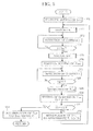
- the timing Ton to turn on the switch element 5 and the timing Toff to turn off the switch element 5 are set according to the processing routine shown in FIG. 5 .
- the timing Ton to turn on the switch element 5 is temporarily set ⁇ Step S21>.
- the switch element 5 is turned on at the timing Ton in sync with the zero-crossing cycle T ⁇ Step S22>.
- the switch element 5 is turned on after a lapse of the first OFF period T1 in which the output current I from the reactor 2 is zero in the initial stage of the cycle T.
- the turn-on timing Ton (first OFF period TI) that is temporarily set may be set as turn-on timing that is fixedly (normally) set in a conventional DC power supply device or may also be set as the zero-crossing point of the AC voltage.
- the current I (short-circuit current Is flowing through the switch element 5) delivered from the reactor 2 at this point of time is detected by the shunt resistance 8 ⁇ Step S23>, and it is determined whether the current I exceeds the threshold current Ith ⁇ Step S24>. This determination processing is repeatedly carried out until the current I detected by the shunt resistance 8 exceeds the threshold current Ith.
- the switch element 5 is turned off ⁇ Step S25>, and the detected timing is temporarily set as the turn-off timing Toff of the switch element 5 ⁇ Step S26>.
- the threshold current Ith used for the determination changes, forming a sine wave along with time lapse, within the cycle T synchronized with the zero-crossing points.
- whether the detected current I exceeds the threshold current Ith can be determined by creating the threshold current Ith forming a half-cycle sine wave during the cycle T in sync with the zero-crossing points and simultaneously comparing the threshold current Ith with the current I that is sequentially detected during the cycle T.
- the current I current Id flowing through the diode 4
- the shunt resistance 8 ⁇ Step S26>.
- a determination is repeatedly made as to whether the current I reaches zero ⁇ Step S27>, and the timing Tend at which the current I flowing through the diode 4 reaches zero is detected ⁇ Step S28>.
- the off period T2 is determined, in which the current I delivered from the reactor 2 is zero in the late stage of the cycle T ⁇ Step S29>.
- the target OFF period T3 is determined, in which the output current I from the reactor 2 should be maintained at zero in the initial stage of the cycle T ⁇ Step S30>.
- the target OFF period T3 is determined as a period in which the output current I of the reactor 2 in the period T is approximate as closely as possible to the sine wave of a half cycle.
- the coefficient ⁇ is set as a value falling in a range, for example, from about 0.5 to about 0.9, in consideration of a difference between a change in the output current Is from the reactor 2, which flows through the switch element 5 when the switch element 5 is in the ON position, and a change in the output current Id from the reactor 2, which flows through the diode 4 when the switch element 5 is in the OFF position.
- the turn-on timing Ton of the switch element 5 can be modified by shifting the preset turn-on timing Ton in increments of predetermined time ⁇ t.
- the turn-on timing Ton of the switch element 5 is modified in the above-described fashion, the timing at which current is delivered from the reactor 2 through the switch element 5 is accordingly changed. As a result, the timing at which the output current I exceeds the threshold current Ith is also changed. The turn-off timing Toff of the switch element 5 is then changed, so that the timing Tend is also changed, at which the current I flowing through the diode 4 reaches zero. Furthermore, the second OFF period T2 is accordingly changed, and so is the target OFF period T3. A determination is made as to whether the turn-on timing Ton of the switch element 5 that is set as mentioned is proper in the target OFF period T3 that is newly set. The foregoing processing is repeatedly carried out until the first period T1 converges at the target OFF period T3.
- the turn-on timing Ton and the turn-off timing Toff of the switch element 5 which are temporarily set at the time, are set as control timings for approximating the output current I from the reactor 2 to the sine wave of a half cycle in a balanced manner and effectively preventing harmonic generation, and these control timings are constantly delivered ⁇ Step S32>.
- the invention is not limited to the embodiment.
- the average current Iave entered into the reactor 2 is evaluated from the output current I delivered from the reactor 2 , and the turn-off timing Toff of the switch element 5 is set on the basis of the threshold current Ith determined by the average current Iave. It is also possible, however, to set the turn-off timing Toff of the switch element 5 in consideration of the output voltage Vout that is smoothed by the condenser 3. More specifically, the voltage Vout smoothed by the condenser 3 and delivered to the load RL is detected, and the turn-off timing Toff of the switch element 5 is modified so that the output voltage Vout approximates to target output voltage that is determined by specifications of the load RL and the like. It is only necessary to repeat this modification processing to converge the turn-off timing Toff of the switch element 5 at optimum timing.
- the invention may be modified in various ways without deviating from the gist thereof.
- the invention is suitable to be used as an excellent DC power supply device that is capable of properly and easily setting the turn-on/off timing of the switch element according to the specifications of an alternator, the use conditions of a DC power supply device, etc.
Landscapes
- Engineering & Computer Science (AREA)
- Power Engineering (AREA)
- Rectifiers (AREA)
- Dc-Dc Converters (AREA)
- Power Conversion In General (AREA)
Abstract
Summary
Purpose: To provide a DC power supply device capable of properly setting the turn-on/off timing of a switch element that short-circuits the output of a reactor and thus controlling harmonic generation.
Means to attain the purpose: A first OFF period in which output current from the reactor is zero in the initial stage of a control cycle is obtained from the turn-on timing of the switch element, and a second OFF period in which the current delivered from the reactor is zero in the late stage of the cycle is obtained from timing at which the current delivered from the reactor becomes zero after the switch element is turned off (first means) . The first means is reactivated after the turn-on timing of the switch element is modified so that the first OFF period approximates to the target OFF period that is set according to the second OFF period, and the turn-on timing of the switch element is set so that the first OFF period and the target OFF period equal to each other (second means).
Description
- The present invention relates to a DC power supply device of a reactor-input type, and more specifically, to a DC power supply device capable of properly setting timing to operate a switch element that short-circuits the output of a reactor, regardless of specifications of AC power or the like.
- A DC power supply device of a reactor-input type is formed chiefly of a
rectifier 1 that full-wave rectifies AC power, areactor 2 that is an inductive element connected to one of the output terminals of therectifier 1, and a condenser 3 that smoothes output from thereactor 2 and supplies the output to load RL, basically as shown inFIG. 1 . In order to prevent harmonic generation in a DC power supply device of this type, it has been suggested to place abackflow preventing diode 4 in series between thereactor 2 and the condenser 3, set aswitch element 5, such as an insulated gate bipolar transistor (IGBT) and a MOS transistor, between thereactor 2 and the other output terminal of therectifier 1, and short-circuit the output of thereactor 2 by turning on theswitch element 5 in sync with its duty cycle (seePatent Document 1, for example). - Patent Document 1: Japanese Patent No.
2763479 - The
switch element 5 short-circuits the output of thereactor 2 and thus approximates a current waveform to a sine wave, which is delivered from thereactor 2 through thediode 4 to the condenser 3, thereby preventing harmonic generation. Whether or not the current waveform can successfully approximate to the sine wave, however, depends greatly upon the turn-on/off timing of theswitch element 5. On top of that, the best turn-on/off timing of theswitch element 5 varies according to the specifications (voltage, frequency) of an alternator, load status, etc. On this account, even if some patterns of turn-on/off timing of theswitch element 5 are previously determined on the assumption of use conditions of a DC power supply device of this type, and these patterns are selectively used to turn on/off theswitch element 5, it is difficult to optimize operating conditions according to a variety of use conditions. - The present invention has been made in light of the above circumstances. It is an object of the invention to provide a DC power supply device capable of preventing harmonic generation by properly setting the turn-on/off timing of a switch element that short-circuits the output of a reactor, regardless of specifications of AC power, load status, etc.
- To achieve the object, in consideration of the current delivered from the reactor and supplied through a diode to load and the current short-circuited by the switch element, a DC power supply device of the invention is designed to effectively prevent harmonic generation, regardless of specifications of AC power, load status, etc., by setting proper timing for turning on/off the switch element through arithmetic processing based upon a time period in which no current flows.
- The DC power supply device of the invention is characterized by having means for entering electric power that is full-wave rectified by a rectifier into a rector and supplying load with output current from the reactor after directing the current to a condenser through a backflow preventing diode for smoothing the current, and a switch element that short-circuits the output of the reactor in sync with a cycle of the full-wave rectified electric power and thus prevents harmonic generation, the device being characterized in that switch control means that includes current-detecting means for sequentially detecting the current delivered from the reactor and performs turn-on/off control of the switch element has first means that determines a first OFF period in which the output current from the reactor is zero in an initial stage of the cycle from turn-on timing of the switch element and determines a second OFF period in which the output current from the reactor is zero in a late stage of the cycle from timing at which the current delivered from the reactor becomes zero after the switch element is turned off; and second means that reactivates the first means after modifying the turn-on timing of the switch element so that the first OFF period approximates to a target OFF period that is determined according to the second OFF period, and sets the turn-on timing of the switch element so that the first OFF period and the target OFF period become equal to each other.
- The target OFF period is determined, for example, by multiplying the second OFF period by a predetermined coefficient. The switch control means is designed to control the turn-on/off timing of the switch element, using as a start point the timing for detecting a zero-crossing point of AC voltage in an alternator, which is entered into the rectifier. The turn-off timing of the switch element is set, for example, as timing at which the current delivered from the reactor exceeds a preset current threshold value. Preferably, the current threshold value is evaluated as a current waveform (sine wave) obtained by multiplying a target current waveform (sine wave) for one duty cycle by a predetermined coefficient, which is evaluated to be equivalent to the amount of current delivered from the reactor to the load during the one duty cycle. It is also possible to set the turn-off timing of the switch element by adjusting DC voltage supplied to the load equals to preset target DC voltage.
- With the DC power supply device thus configured, the turn-on timing of the switch element can be properly set by predetermined arithmetic processing on the basis of a period in which the current delivered from the reactor, especially, the current supplied through the diode to the condenser, is zero. Moreover, the turn-off timing of the switch element can also be properly set on the basis of the current short-circuited by the switch element. In short, the turn-on/off timing of the switch element can be properly and easily set according to specifications of an alternator, use conditions of the DC power supply device, etc. Harmonic generation can be prevented with efficiency, regardless of the specifications of the alternator, load status, etc.
- Even if the turn-on/off timing of the switch element is beforehand normally set, the turn-on/off timing of the switch element is modified by degree according to the current delivered from the reactor on the basis of the use conditions of the device, and is thus made proper. Consequently, harmonic generation can be effectively prevented according to various kinds of usage environment.
-
-
FIG. 1 is a diagram showing a configuration of a DC power supply device according to one embodiment of the invention; -
FIG. 2 is an operating waveform chart for explaining basic operations of the DC power supply device; -
FIG. 3 is a view for explaining operations associated with turn-on/off of a switch element in the DC power supply device of the invention; -
FIG. 4 is a view showing one example of a routine of an initial setting processing for the DC power supply device according to one embodiment of the invention; and -
FIG. 5 is a view showing one example of a routine of setting turn-on/off timing of a switch element in the DC power supply device according to one embodiment of the invention. - A DC power supply device according to one embodiment of the invention will be described below with reference to the drawings. This DC power supply device is of a so-called reactor-input type. Basically, the device is formed chiefly of a
rectifier 1 that full-wave rectifies AC power as shown inFIG. 1 , areactor 2 that is an inductive element whose first end is connected to a plus output terminal of therectifier 1, and a condenser 3 that is connected between a second end of thereactor 2 and a minus output terminal of therectifier 1 and supplies an output current from thereactor 2 to load RL after smoothing the current. Abackflow preventing diode 4 is serially interposed between the second end of thereactor 2 and the condenser 3. Connected between the second end of thereactor 2 and the minus output terminal of therectifier 1 is aswitch element 5 that short-circuits thereactor 2 and discontinues current supply to the load side. Theswitch element 5 is made up of an IGBT and a MOS transistor which are turned on/off (ON-OFF controlled) by a switch controller (switch controlling means) 6. - The
switch controller 6 functions to turn on/off theswitch element 5 at predetermined timing, basically using as synchronization reference timing a zero-crossing point of the alternator, which is detected by a zero-crossing detector 7. In general, theswitch controller 6 installed in a conventional DC power supply device fixes turn-on/off timing of theswitch element 5 according to the specifications of a power supply or selects one of prepared patterns of turn-on/off timing according to load specification and the use conditions of the power supply device. - In this respect, in the DC power supply device according to the present embodiment, a
shunt resistance 8 is serially placed on the minus output terminal side of therectifier 1. Theswitch controller 6 properly sets turn-on timing Ton and turn-off timing Toff of theswitch element 5 as mentioned later on the basis of output current of thereactor 2, which is detected by theshunt resistance 8. Current I detected by theshunt resistance 8 is the output current from thereactor 2 short-circuited by theswitch element 5 when theswitch element 5 is in the ON position. When theswitch element 5 is in the OFF position, the current I is the current supplied from thereactor 2 through thediode 4 to the condenser 3 and thus to the load RL side. - Firstly, basic operations of the DC power supply device will be described. Input voltage Vin that is full-wave rectified by the
rectifier 1 and entered into thereactor 2 is, as shown inFIG. 2 , a half-cycle sine wave (plus component) whose reference point is a zero-crossing point of the alternator. A cycle T of the half-cycle sine wave is half of a cycle of an AC voltage waveform. If theswitch element 5 is constantly in the OFF position, input current Iin that flows in through thereactor 2 is increased by degree to charge the condenser 3 from a time point at which the input voltage Vin exceeds a charge voltage (smoothed output voltage Vout) of the condenser 3 as shown inFIG. 2 . The input current Iin is then gradually decreased along with a reduction of the input voltage Vin and reaches zero when the input voltage Vin is decreased to the charge voltage of the condenser 3. - If the
switch element 5 is turned on/off at preset timing, the input current Iin that flows in through thereactor 2 starts flowing from a time point Ton at which theswitch element 5 is turned on and is gradually increased as shown inFIG. 3 . The input current Iin flows in through thediode 4 to charge the condenser 3 from a time point Toff at which theswitch element 5 is turned off. When theswitch element 5 is in the ON position (ON period,), the input current Iin is all short-circuited by theswitch element 5, and is not supplied to the condenser 3 (load RL side) through thediode 4. In this process, if the input current Iin that flows in through thereactor 2 is made to be approximate as closely as possible to a sine wave, harmonic generation can be prevented. In this view, in order to achieve the input current Iin approximate to the sine wave, it is important to properly set the turn-on timing Ton and the turn-off timing Toff of theswitch element 5. - According to the invention, the turn-off timing Toff of the
switch element 5 is set in consideration of average current Iave flowing during the cycle T of the current I delivered from thereactor 2, and the turn-on timing Ton of theswitch element 5 is properly set on the basis of timing at which the current I becomes zero after theswitch element 5 is turned off. The average input current Iave flowing during the cycle T of the current I delivered from thereactor 2 is defined as current (half-cycle sine wave) in which a current amount ΣI that is an integrated value of the output current I from thereactor 2 within the cycle T as shown inFIG. 2 is averagely entered into thereactor 2 according to the input voltage Vin. A current amount ΣIave of the current Iave is determined to be equal to the current amount ΣI. - The present embodiment sets as the turn-off timing Toff of the
switch element 5 the timing at which the current I delivered from thereactor 2 by the turn-on of theswitch element 5 exceeds threshold current Ith shown inFIG. 3 , which is evaluated by multiplying the average current Iave by a predetermined coefficient α (>1.) . In other words, the turn-on of theswitch element 5 causes the current I to be delivered from thereactor 2, and the output current I is increased by degree. Based upon the fact that, if theswitch element 5 is turned off at a time point when the current I is increased to some degree, the current I flowing from thereactor 2 through thediode 4 into the condenser 3 is thereafter continuously delivered, the turn-off timing of theswitch element 5 is set according to the magnitude of the current I delivered from thereactor 2. - In order to properly set the turn-on timing Ton of the
switch element 5, a first OFF period TI in which the input current Iin is maintained at zero in an initial stage of the cycle T is determined from the turn-on timing Ton of theswitch element 5, which is temporarily set. At the same time, a second OFF period T2 in which the input current Iin becomes zero in a late stage of the cycle T is determined from timing Tend at which the input current Iin (current supplied through thediode 4 to the condenser 3) becomes zero after theswitch element 5 is turned off [first means]. - A target OFF period T3 in the initial stage is determined on the basis of the second OFF period T2 determined as described above, and the first OFF period Tl, or more specifically, the turn-on timing Ton of the
switch element 5, is changed so as to approximate to the target OFF period T3 [second means]. Along with the change of the turn-on timing Ton of theswitch element 5, the timing at which the current I delivered from thereactor 2 exceeds the threshold current Ith is changed. On this account, the turn-off timing Toff of theswitch element 5 is accordingly changed. This consequently changes the timing Tend at which the current (output current I) that is supplied from thereactor 2 through thediode 4 to the condenser 3 after theswitch element 5 is turned off, thereby changing the second OFF period T2. - Given the foregoing factor, under the conditions where the turn-on timing Ton of the
switch element 5 is changed, the processing in the first means is carried out again [second means], and the second OFF period T2 is newly determined, to thereby set a new target OFF period T3. If the processing is repeatedly carried out, the first OFF period T1 gradually converges at the target OFF period T3 that is newly determined, which optimizes the turn-on timing Ton and the turn-off timing Toff of theswitch element 5. -
FIG. 4 shows one example of a routine of an initial setting processing in the DC power supply device according to the invention, which is configured to set the turn-on timing Ton and the turn-off timing Toff of theswitch element 5 as described above. The initial setting processing includes the steps of determining a control cycle T of theswitch element 5 on the basis of a cycle of the AC voltage waveform, calculating the average current Iave entered into thereactor 2 on the basis of the output current I from thereactor 2, and setting the threshold current Ith for setting the turn-off timing Toff of theswitch element 5 on the basis of the average current Iave . - The control cycle T of the
switch element 5 is determined basically as a cycle of the zero-crossing point of AC voltage, which is detected by the zero-crossingdetector 7. The frequency of the alternator is maintained substantially constant in the long term but is varied (fluctuated) in some small measure in the short term. In other words, the AC voltage cycle itself is varied (fluctuated) in some small measure. Depending upon regions or countries in which the DC power supply device is used, the alternator frequency itself varies, and it is not very likely that the stability of power-supply frequency is uniform. - Firstly in order that the control cycle T of the
switch element 5 may be stably set without being affected by the fluctuation in the cycle of the alternator, the present embodiment determines the control cycle T of theswitch element 5 as an average value of a cycle of the zero-crossing point detected N times (50 times, for example) by the zero-crossingdetector 7. To be specific, a parameter n for cycle detection is initialized at zero <Step S1>. While this control parameter n is incremented <Step S2>, a period Tn (n=1 to N) between zero-crossing points of AC voltage, which are detected by the zero-crossingdetector 7, is detected <Step S3>. A determination is made as to whether the detected period (zero-crossing cycle) Tn falls in a predetermined range of from Tmin to Tmax <Step S4>. If the period Tn is outside the range, the obtained data (detected period Tn) is discarded <Step S5>. This processing is repeatedly carried out until N pieces of data (detected period Tn) are obtained <Step S6>. An average value of the N pieces of data is set as the control cycle T of theswitch element 5 <Step S7>. - Considering the fact that the frequency of the alternator is normally 50 Hz or 60 Hz, it is appropriate if the range of determination of the zero-crossing cycle Tn extends, for example, from a minimum cycle of 15.385 mSec where the power-supply frequency is higher than 65 Hz to a maximum cycle of 22.222 mSec where the power-supply frequency is lower than 45 Hz. In stead of evaluating the average value of zero-crossing input as mentioned, it is also possible to evaluate an average zero-crossing cycle Tn through filtering processing and set the average zero-crossing cycle Tn as the control cycle T of the
switch element 5. - Thereafter, the threshold current Ith for defining the turn-off timing Toff of the
switch element 5 is determined. This processing is carried out under such ideal conditions that theswitch element 5 is brought into a constant OFF position (no turn-on/off control is conducted), and that the output current I from thereactor 2 is all supplied through thediode 4 to the condenser 3 (load RL side) step S11>. In this state, the output current I (current Id flowing through the diode 4) is sequentially defected by theshunt resistance 8 during the cycle T that is set as described above <Step S12>. The current defection is performed in a sampling cycle of, for example, from 100 µSee to 200 µSec. - Next, on the basis of the integrated value ΣI of the output current I (current Id flowing through the diode 4) detected during the cycle T, the average current Iave is evaluated, which is averagely entered into the
reactor 2, forming a sine wave, during the cycle T according to the input voltage Vin <Step S13>. Instead of evaluating the integrated value ΣI of the output current I, it is also possible to evaluate an average value of the output current I flowing during the cycle T and evaluate the average current Iave that is averagely entered into thereactor 2, forming a sine wave, during the cycle T according to the average value of the output current I. - Based upon the average current Iave, the threshold current Ith for defining the turn-off timing Toff of the
switch element 5 is determined, for example, by the formula: Ith=α×Iave <Step S14>. The coefficient α is set as a value falling in a range, for example, from about 1.1 to about 1.3 in anticipation of current Is that is not supplied through thediode 4 to the condenser 3 along with the turn-on/off control of theswitch element 5 and is short-circuited by theswitch element 5. - If the initial setting processing is finished in the foregoing manner, the timing Ton to turn on the
switch element 5 and the timing Toff to turn off theswitch element 5 are set according to the processing routine shown inFIG. 5 . Firstly, the timing Ton to turn on theswitch element 5 is temporarily set <Step S21>. Secondarily, theswitch element 5 is turned on at the timing Ton in sync with the zero-crossing cycle T <Step S22>. In other words, theswitch element 5 is turned on after a lapse of the first OFF period T1 in which the output current I from thereactor 2 is zero in the initial stage of the cycle T. The turn-on timing Ton (first OFF period TI) that is temporarily set may be set as turn-on timing that is fixedly (normally) set in a conventional DC power supply device or may also be set as the zero-crossing point of the AC voltage. - The current I (short-circuit current Is flowing through the switch element 5) delivered from the
reactor 2 at this point of time is detected by theshunt resistance 8 <Step S23>, and it is determined whether the current I exceeds the threshold current Ith <Step S24>. This determination processing is repeatedly carried out until the current I detected by theshunt resistance 8 exceeds the threshold current Ith. When the current I exceeds the threshold current Ith, theswitch element 5 is turned off <Step S25>, and the detected timing is temporarily set as the turn-off timing Toff of theswitch element 5 <Step S26>. - As shown in
FIG. 3 , the threshold current Ith used for the determination changes, forming a sine wave along with time lapse, within the cycle T synchronized with the zero-crossing points. In this light, whether the detected current I exceeds the threshold current Ith can be determined by creating the threshold current Ith forming a half-cycle sine wave during the cycle T in sync with the zero-crossing points and simultaneously comparing the threshold current Ith with the current I that is sequentially detected during the cycle T. - After the
switch element 5 is turned off in this way, the current I (current Id flowing through the diode 4) that is delivered from thereactor 2 and supplied through thediode 4 to the condenser 3 is detected by theshunt resistance 8 <Step S26>. At the same time, a determination is repeatedly made as to whether the current I reaches zero <Step S27>, and the timing Tend at which the current I flowing through thediode 4 reaches zero is detected <<Step S28>. Based upon the detected timing Tend, the off period T2 is determined, in which the current I delivered from thereactor 2 is zero in the late stage of the cycle T <Step S29>. Based upon the second OFF period T2, the target OFF period T3 is determined, in which the output current I from thereactor 2 should be maintained at zero in the initial stage of the cycle T <Step S30>. - The target OFF period T3 is determined as a period in which the output current I of the
reactor 2 in the period T is approximate as closely as possible to the sine wave of a half cycle. The target OFF period T3 is therefore determined, for example, by the formula: T3=β×T2. The coefficient β is set as a value falling in a range, for example, from about 0.5 to about 0.9, in consideration of a difference between a change in the output current Is from thereactor 2, which flows through theswitch element 5 when theswitch element 5 is in the ON position, and a change in the output current Id from thereactor 2, which flows through thediode 4 when theswitch element 5 is in the OFF position. - A determination is made as to whether the first OFF period T1 is equal to the target OFF period T3 that is set as described above <Step S31>. If the periods T1 and T2 are not equal to each other, the turn-on timing Ton of the
switch element 5 is modified to approximate the first OFF period T1to the target OFF period T3 <Step S32>. The turn-on control of theswitch element 5 is conducted at the modified turn-on timing Ton, to thereby repeat the processing starting from Step S23. The turn-on timing Ton of theswitch element 5 can be modified by shifting the preset turn-on timing Ton in increments of predetermined time Δt. - If the turn-on timing Ton of the
switch element 5 is modified in the above-described fashion, the timing at which current is delivered from thereactor 2 through theswitch element 5 is accordingly changed. As a result, the timing at which the output current I exceeds the threshold current Ith is also changed. The turn-off timing Toff of theswitch element 5 is then changed, so that the timing Tend is also changed, at which the current I flowing through thediode 4 reaches zero. Furthermore, the second OFF period T2 is accordingly changed, and so is the target OFF period T3. A determination is made as to whether the turn-on timing Ton of theswitch element 5 that is set as mentioned is proper in the target OFF period T3 that is newly set. The foregoing processing is repeatedly carried out until the first period T1 converges at the target OFF period T3. - When the first period T1 converges at the target OFF period T3 <Step S32>, the turn-on timing Ton and the turn-off timing Toff of the
switch element 5, which are temporarily set at the time, are set as control timings for approximating the output current I from thereactor 2 to the sine wave of a half cycle in a balanced manner and effectively preventing harmonic generation, and these control timings are constantly delivered <Step S32>. - With the DC power supply device that sets the turn-on timing Ton and the turn-off timing Toff of the
switch element 5 in the above fashion, it is possible to approximate the current waveform delivered from thereactor 2 to the sine wave of the half cycle in a balanced manner, so that harmonic generation is effectively prevented. Even if the frequency (cycle) of the alternator is unknown or if the frequency (cycle) largely fluctuates or if the operating conditions are drastically changed due to a difference in the load RL, the turn-on/off timings Ton and Toff of theswitch element 5 can be properly set with ease and efficiency. Consequently, there is a great deal of practical advantage in preventing harmonic generation in the DC power supply device of a reactor-input type, which is used under various conditions. - The invention is not limited to the embodiment. According to the embodiment, the average current Iave entered into the
reactor 2 is evaluated from the output current I delivered from thereactor 2 , and the turn-off timing Toff of theswitch element 5 is set on the basis of the threshold current Ith determined by the average current Iave. It is also possible, however, to set the turn-off timing Toff of theswitch element 5 in consideration of the output voltage Vout that is smoothed by the condenser 3. More specifically, the voltage Vout smoothed by the condenser 3 and delivered to the load RL is detected, and the turn-off timing Toff of theswitch element 5 is modified so that the output voltage Vout approximates to target output voltage that is determined by specifications of the load RL and the like. It is only necessary to repeat this modification processing to converge the turn-off timing Toff of theswitch element 5 at optimum timing. In addition, the invention may be modified in various ways without deviating from the gist thereof. - The invention is suitable to be used as an excellent DC power supply device that is capable of properly and easily setting the turn-on/off timing of the switch element according to the specifications of an alternator, the use conditions of a DC power supply device, etc.
-
- 1
- rectifier
- 2
- reactor
- 3
- condenser
- 4
- diode (for backflow prevention)
- 5
- switch element (IGBT or MOS transistor)
- 6
- switch controller
- 7
- zero-crossing detector
- 8
- shunt resistance (current-detecting means)
- RL
- load
Claims (5)
- A DC power supply device having means for entering electric power that is full-wave rectified by a rectifier into a rector and supplying load with output current from the reactor after directing the current to a condenser through a backflow preventing diode for smoothing the current, and a switch element that short-circuits the output of the reactor in sync with a cycle of the full-wave rectified power supply and thus prevents harmonic generation, the device being characterized in that:switch control means that includes current-detecting means for sequentially detecting the current delivered from the reactor and performs turn-on/off control of the switch element has: first means that determines a first OFF period in which the output current from the reactor is zero in an initial stage of the cycle from turn-on timing of the switch element and determines a second OFF period in which the output current from the reactor is zero in a late stage of the cycle from timing at which the current delivered from the reactor becomes zero after the switch element is turned off; andsecond means that reactivates the first means after modifying the turn-on timing of the switch element so that the first OFF period approximates to a target OFF period that is determined according to the second OFF period, and sets the turn-on timing of the switch element so that the first OFF period and the target OFF period become equal to each other.
- The DC power supply device according to claim 1, wherein:the target OFF period is determined by multiplying the second OFF period by a predetermined coefficient.
- The DC power supply device according to claim 1, wherein:the switch control means detects the cycle of the full-wave rectified power supply from detected timing of a zero-crossing point of AC voltage in an alternator, which is entered into the rectifier, and controls the turn-onjoff timing of the switch element, using as a start point of a duty cycle the detected timings of the zero-crossing point.
- The DC power supply device according to claim 1, wherein:the turn-off timing of the switch element is set as timing at which the current delivered from the reactor exceeds a preset current threshold value; andthe current threshold value is evaluated as a current waveform obtained by multiplying a target current waveform for one duty cycle by a predetermined coefficient, which is evaluated to be equivalent to the amount of current delivered from the reactor to the load during the one duty cycle.
- The DC power supply device according to claim 1, wherein:the turn-off timing of the switch element is adjusted so that DC voltage supplied to the load equals to preset target DC voltage.
Applications Claiming Priority (2)
| Application Number | Priority Date | Filing Date | Title |
|---|---|---|---|
| JP2009076171A JP5180890B2 (en) | 2009-03-26 | 2009-03-26 | DC power supply |
| PCT/JP2010/001925 WO2010109820A1 (en) | 2009-03-26 | 2010-03-18 | Dc power supply device |
Publications (1)
| Publication Number | Publication Date |
|---|---|
| EP2413486A1 true EP2413486A1 (en) | 2012-02-01 |
Family
ID=42780519
Family Applications (1)
| Application Number | Title | Priority Date | Filing Date |
|---|---|---|---|
| EP10755623A Withdrawn EP2413486A1 (en) | 2009-03-26 | 2010-03-18 | Dc power supply device |
Country Status (4)
| Country | Link |
|---|---|
| EP (1) | EP2413486A1 (en) |
| JP (1) | JP5180890B2 (en) |
| CN (1) | CN102362421A (en) |
| WO (1) | WO2010109820A1 (en) |
Families Citing this family (3)
| Publication number | Priority date | Publication date | Assignee | Title |
|---|---|---|---|---|
| JP5471513B2 (en) * | 2010-01-27 | 2014-04-16 | 株式会社富士通ゼネラル | Power supply |
| KR101734683B1 (en) | 2015-10-07 | 2017-05-11 | 현대자동차주식회사 | Power Distibuting Block Of Vehicle |
| CN115328253B (en) * | 2022-08-29 | 2024-04-05 | 珠海市伟高变频科技有限公司 | Single-phase PFC circuit without input voltage detection and voltage estimation method thereof |
Family Cites Families (5)
| Publication number | Priority date | Publication date | Assignee | Title |
|---|---|---|---|---|
| JP2763479B2 (en) * | 1992-08-06 | 1998-06-11 | 三菱電機株式会社 | DC power supply |
| JP3726611B2 (en) * | 2000-01-17 | 2005-12-14 | 松下電器産業株式会社 | Air conditioner power circuit |
| JP2002345250A (en) * | 2001-05-11 | 2002-11-29 | Tdk Corp | Rectifier circuit |
| CN1592067A (en) * | 2003-08-28 | 2005-03-09 | 松下电器产业株式会社 | Power supply device and air-conditioner using the same |
| KR20050111204A (en) * | 2004-05-21 | 2005-11-24 | 엘지전자 주식회사 | Method for power factor compensation of inverter control circuit |
-
2009
- 2009-03-26 JP JP2009076171A patent/JP5180890B2/en not_active Expired - Fee Related
-
2010
- 2010-03-18 EP EP10755623A patent/EP2413486A1/en not_active Withdrawn
- 2010-03-18 CN CN2010800140280A patent/CN102362421A/en active Pending
- 2010-03-18 WO PCT/JP2010/001925 patent/WO2010109820A1/en not_active Ceased
Non-Patent Citations (1)
| Title |
|---|
| See references of WO2010109820A1 * |
Also Published As
| Publication number | Publication date |
|---|---|
| JP5180890B2 (en) | 2013-04-10 |
| JP2010233296A (en) | 2010-10-14 |
| CN102362421A (en) | 2012-02-22 |
| WO2010109820A1 (en) | 2010-09-30 |
Similar Documents
| Publication | Publication Date | Title |
|---|---|---|
| CN104242660B (en) | Switch power supply equipment, Switching Power Supply control method and electronic device | |
| US8508195B2 (en) | PFC converter using a predetermined value that varies in synchronization with a phase of the input voltage | |
| US8379420B2 (en) | Controller with punctuated switching control circuit | |
| US9455623B2 (en) | Power factor correction circuit and method | |
| US8183839B2 (en) | Switching power source system | |
| US11404962B2 (en) | Switched mode power converter that is switched using current thresholds | |
| US8891259B2 (en) | Control circuit and method for audible noise suppression in a power converter | |
| US9750102B1 (en) | Switch current control to shape input current | |
| US8854016B2 (en) | Power supply apparatus | |
| CN105049034A (en) | Current pulse count control in a voltage regulator | |
| US20200220452A1 (en) | Enhanced power factor correction | |
| JP6103348B2 (en) | Power supply circuit and lighting device | |
| US11968765B2 (en) | Induction cooking system | |
| CN103814511B (en) | For the Method and circuits of PFC | |
| JP6379877B2 (en) | High efficiency power factor correction circuit and switching power supply | |
| CN102362421A (en) | DC power supply unit | |
| US11165357B2 (en) | Control gear for an electrical load and method | |
| US12348054B2 (en) | Wireless power transmitter circuit having OVP control for receiver circuit and control circuit and method thereof | |
| WO2012146695A2 (en) | Electronic driver for a lightsource | |
| US12047001B2 (en) | Zero-crossing correction circuit and zero-crossing correction method for a switching converter | |
| KR100283147B1 (en) | How to drive BCD motor of inverter refrigerator | |
| CN101164391A (en) | Electronic ballast capable of reducing reactive current oscillations | |
| KR20000046280A (en) | Method for monitoring non-operative mode of induction heating cooker |
Legal Events
| Date | Code | Title | Description |
|---|---|---|---|
| PUAI | Public reference made under article 153(3) epc to a published international application that has entered the european phase |
Free format text: ORIGINAL CODE: 0009012 |
|
| 17P | Request for examination filed |
Effective date: 20110923 |
|
| AK | Designated contracting states |
Kind code of ref document: A1 Designated state(s): AT BE BG CH CY CZ DE DK EE ES FI FR GB GR HR HU IE IS IT LI LT LU LV MC MK MT NL NO PL PT RO SE SI SK SM TR |
|
| DAX | Request for extension of the european patent (deleted) | ||
| STAA | Information on the status of an ep patent application or granted ep patent |
Free format text: STATUS: THE APPLICATION IS DEEMED TO BE WITHDRAWN |
|
| 18D | Application deemed to be withdrawn |
Effective date: 20141001 |