EP2413448A2 - Active AC inrush current control - Google Patents
Active AC inrush current control Download PDFInfo
- Publication number
- EP2413448A2 EP2413448A2 EP11175669A EP11175669A EP2413448A2 EP 2413448 A2 EP2413448 A2 EP 2413448A2 EP 11175669 A EP11175669 A EP 11175669A EP 11175669 A EP11175669 A EP 11175669A EP 2413448 A2 EP2413448 A2 EP 2413448A2
- Authority
- EP
- European Patent Office
- Prior art keywords
- state
- transistor
- states
- current
- semiconductor switching
- Prior art date
- Legal status (The legal status is an assumption and is not a legal conclusion. Google has not performed a legal analysis and makes no representation as to the accuracy of the status listed.)
- Withdrawn
Links
Images


Classifications
-
- H—ELECTRICITY
- H02—GENERATION; CONVERSION OR DISTRIBUTION OF ELECTRIC POWER
- H02H—EMERGENCY PROTECTIVE CIRCUIT ARRANGEMENTS
- H02H9/00—Emergency protective circuit arrangements for limiting excess current or voltage without disconnection
- H02H9/001—Emergency protective circuit arrangements for limiting excess current or voltage without disconnection limiting speed of change of electric quantities, e.g. soft switching on or off
-
- H—ELECTRICITY
- H02—GENERATION; CONVERSION OR DISTRIBUTION OF ELECTRIC POWER
- H02H—EMERGENCY PROTECTIVE CIRCUIT ARRANGEMENTS
- H02H9/00—Emergency protective circuit arrangements for limiting excess current or voltage without disconnection
- H02H9/001—Emergency protective circuit arrangements for limiting excess current or voltage without disconnection limiting speed of change of electric quantities, e.g. soft switching on or off
- H02H9/002—Emergency protective circuit arrangements for limiting excess current or voltage without disconnection limiting speed of change of electric quantities, e.g. soft switching on or off limiting inrush current on switching on of inductive loads subjected to remanence, e.g. transformers
-
- H—ELECTRICITY
- H02—GENERATION; CONVERSION OR DISTRIBUTION OF ELECTRIC POWER
- H02H—EMERGENCY PROTECTIVE CIRCUIT ARRANGEMENTS
- H02H9/00—Emergency protective circuit arrangements for limiting excess current or voltage without disconnection
- H02H9/02—Emergency protective circuit arrangements for limiting excess current or voltage without disconnection responsive to excess current
- H02H9/025—Current limitation using field effect transistors
Definitions
- an initial inrush current may be several times a normal steady state rated current.
- the inrush current may be caused by charging a direct current (DC) link capacitor and/or energizing an un-energized transformer or filter magnetics.
- a soft start configuration may be used to limit the inrush current to an acceptable level.
- FIG. 2 A further system for AC inrush current control is illustrated in FIG. 2 .
- the system 200 includes three resistors 201, 210, and 211 in communication with three-phase power denoted by phases A, B, and C.
- the resistors 201, 210, and 211 are in further communication with rectifier 203.
- the rectifier 203 may or may not include a transformer.
- the system 200 further includes bypass switches 202, 220, and 221, configured to bypass the resistors 201, 210, and 211 for full current flow after inrush current has dissipated.
- the system 200 further includes DC link capacitor 205 coupled across lines 231 and 232 which are in communication with the rectifier 203 and load 204.
- a method of active inrush current control includes activating a load, the activating causing inrush current to flow, switching a semiconductor switching device to a current limiting state in response to the inrush current flow, the current limiting state being one of at least three states of the semiconductor switching device and the current limiting state dissipating the inrush current, and switching the semiconductor device to a full current flow state in response to the dissipating, the full current flow state not inhibiting current flow.
- a semiconductor switching device for active inrush current control includes a first transistor disposed and configured to control current flow in at least three states, a first voltage suppression device in communication with the first transistor, a second transistor disposed and configured to control current flow in at least three states, an emitter of the second transistor in communication with an emitter of the first transistor, a second voltage suppression device in communication with the second transistor, and a signaling source in communication with the first transistor and the second transistor, the signaling source disposed and configured to provide different bias voltages to the transistor, the different biasing voltages changing the states of the transistors to a different states of at least three operating states in unison.
- a semiconductor switching device for active inrush current control includes a transistor disposed and configured to control current flow in at least three states, a first diode, a p-type portion of the first diode being in communication with a collector of the transistor, a second diode, a p-type portion of the second diode being in communication with a collector of the transistor, a third diode, an n-type portion of the third diode being in communication with an emitter of the transistor, and a fourth diode being, an n-type portion of the fourth diode being in communication with an emitter of the transistor.
- FIG. 3 illustrates a system for active AC inrush current control, according to an example embodiment
- FIG. 4B illustrates an equivalent circuit for a unidirectional semiconductor switching device for active AC inrush current control, according to an example embodiment
- FIG. 8 illustrates a bidirectional semiconductor switching device for active AC inrush current control, according to an example embodiment
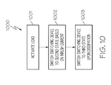
- FIG. 10 illustrates a method of active AC inrush current control, according to an example embodiment.
- the devices 301-303 are in further communication with a rectifier 304, and are disposed to actively alter current flowing between phase input lines A, B, and C, and the rectifier 304.
- the devices 301-303 may actively alter the current flow through switching between the at least three states noted above.
- the rectifier 304 which includes a transformer
- the DC link capacitor 306 may introduce inrush current when activated, for example, if the devices 301-303 are switched to an on-state. Therefore, the devices 301-303 may be switched to a linear state (second state) where current is limited until the rectifier 304 and the DC link capacitor 306 are charged. Upon charging, the devices 301-303 may be switched to an on-state.
- the device 400 further includes signal resistor R1 coupled from input line 411 to the base of transistor 402.
- the device 400 further includes signal resistor R2 coupled from the gate of transistor 402 to zener diode 403, which is further coupled to output line 410.
- Zener diode 403 accounts for a gate threshold voltage of the transistor 402, while the signal resistors R1 and R2 set the equivalent resistance seen between a collector and an emitter of the transistor 402.
- FIG. 4B illustrates an equivalent circuit 405 of the equivalent resistance R seen between the collector and emitter of the transistor 402.
- R th V th / I c
- I c is a rated load current through the collector of the transistor 402
- V th is the gate threshold voltage of the transistor 402
- Vg is the gate voltage of the transistor 402.
- FIG. 5 illustrates a unidirectional semiconductor switching device 500 for active AC inrush current control, according to an example embodiment.
- the device 500 includes transistor 507, bypass and protection diode 508, signal resistor 504, signal resistor 505, and zener diode 506 which are substantially similar in both structure and operation to transistor 402, diode 401, signal resistor R1, signal resistor R2, and zener diode 403. Thus, exhaustive description of these elements is omitted herein for the sake of brevity.
- the device 500 further includes gate drive signal 501.
- Gate drive signal 501 is modeled as a voltage source here for simplicity and illustrative purposes but it should be apparent that the illustrated source 501 may be any suitable voltage signal source producing sufficient voltage to actively switch transistor 507 between at least three states as described above.
- the device 630 may operate in one of at least three states as described above with reference to FIG. 5 .
- FIG. 7 illustrates a bidirectional semiconductor device 700 for active inrush current control, according to an example embodiment.
- the device 700 includes a unidirectional semiconductor switching device 730 which is somewhat similar to unidirectional semiconductor switching device 630.
- the device 730 includes a transistor 707, voltage clamping zener diode 705, bypass and protection diode 706, gate threshold diode 709, signal resistors 708 and 710, and resistor 711.
- a signal source may be in communication with the resistor 711 to allow for three-state operation of the device 730.
- the entire bidirectional device 700 includes a plurality of diodes 701, 702, 703, and 704 in operative communication with the device 730, and input and output lines 720 and 721.
- a p-type portion of the diode 701 is in communication with a collector of the transistor 707.
- a p-type portion of the diode 702 is in communication with the collector of the transistor 707.
- an n-type portion of the diode 703 is in communication with an emitter of the transistor 707.
- an n-type portion of the diode 704 is in communication with the emitter of the transistor 707.
- the diodes 701-704 switch from being forward to reverse biased, and vice versa.
- the diode 702 and 703 are forward biased, allowing for current to be controlled at the device 730 as described above.
- the diodes 701 and 704 are forward biased, allowing for current to be controlled at the device 730 as described above. In this manner, the entire device 700 allows for bidirectional control of current albeit using only a single unidirectional device 730.
- FIG. 8 illustrates a bidirectional semiconductor device 800 for active AC inrush current control, according to an example embodiment.
- the device 800 includes two unidirectional semiconductor switching devices 830 and 831.
- the unidirectional devices 830 and 831 are somewhat similar to devices 630 and 631, but include transorbs 801 and 802 for voltage suppression.
- the bidirectional device 800 is structurally and operationally similar to the device 600.
- the unidirectional device 830 includes transistor 804, diode 803, gate threshold voltage diode 815, signal resistors 807 and 808, and resistor 809. Further, the device 830 includes signal source 810 providing for three-state operation of the device 830.
- FIG. 9 illustrates a bidirectional semiconductor device 900 for active AC inrush current control, according to an example embodiment.
- the device 900 is similar to the device 700, with the inclusion of a single unidirectional device 930.
- the device 930 is somewhat similar to unidirectional semiconductor switching device 830.
- the device 930 includes transorb 905, diode 911, transistor 910, gate threshold diode 909, signal resistors 907 and 908, and resistor 906. Although not specifically illustrated, it should be understood that a signal source may be in communication with the resistor 906 to allow for three-state operation of the device 930.
- the entire bidirectional device 900 includes a plurality of diodes 901, 902, 903, and 904 in operative communication with the device 930, and input and output lines 920 and 921.
- a p-type portion of the diode 901 is in communication with a collector of the transistor 910.
- a p-type portion of the diode 902 is in communication with the collector of the transistor 910.
- an n-type portion of the diode 903 is in communication with an emitter of the transistor 910.
- an n-type portion of the diode 904 is in communication with the emitter of the transistor 910.
- the diodes 901-904 switch from being forward to reverse biased, and vice versa.
- the diode 902 and 903 are forward biased, allowing for current to be controlled at the device 930 as described above.
- the diodes 901 and 904 are forward biased, allowing for current to be controlled at the device 930 as described above. In this manner, the entire device 900 allows for bidirectional control of current albeit using only a single unidirectional device 930.
- FIG. 10 illustrates a method 1000 of active inrush current control, according to an example embodiment.
- the method 1000 further includes switching a semiconductor switching device's operating state in response to inrush current at block 1002.
- a semiconductor switching device may be switched to a current limiting state.
- the semiconductor switching device may be any of the devices described above.
- the current limiting state may be a second state as described above.
- example embodiments of the present invention further provide methods of active inrush current control.
- example embodiments include relatively decreased DC link and transformer based AC inrush current.
- active control of inrush current is possible with relatively little change to control systems.
Landscapes
- Engineering & Computer Science (AREA)
- Power Engineering (AREA)
- Emergency Protection Circuit Devices (AREA)
- Rectifiers (AREA)
Abstract
Description
- The subject matter disclosed herein relates generally to the field of alternating current (AC), and more particularly to active control of AC inrush current.
- When energizing a three phase load such as a frequency converter or motor controller, an initial inrush current may be several times a normal steady state rated current. The inrush current may be caused by charging a direct current (DC) link capacitor and/or energizing an un-energized transformer or filter magnetics. A soft start configuration may be used to limit the inrush current to an acceptable level.
- Conventional soft start configurations limit the DC link current by placing inrush limiting resistors near a DC link. For example,
FIG. 1 depicts such a configuration. Thesystem 100 includes arectifier 104 in communication with three-phase power denoted by phases A, B, and C. Therectifier 104 may or may not include a transformer. Thesystem 100 further includesresistors rectifier 104 and aload 105 overlines system 100 further includes aDC link capacitor 103 coupled acrosslines - As illustrated, the
system 100 includesbypass switches bypass resistors system 100 limits inrush current caused by charging theDC link capacitor 103. For example, during initial charging of theDC link capacitor 103, thebypass switches resistors bypass switches rectifier 104 and theload 105. However, it is apparent that thebypass switching system 100 does not limit inrush current caused by therectifier 104. - Other implementations of the
system 100 may include pulse width modulation of thebypass switches system 100. - A further system for AC inrush current control is illustrated in
FIG. 2 . As illustrated, thesystem 200 includes threeresistors resistors rectifier 203. Therectifier 203 may or may not include a transformer. Thesystem 200 further includesbypass switches resistors system 200 further includesDC link capacitor 205 coupled acrosslines rectifier 203 andload 204. In thesystem 200, inrush current may be limited throughresistors rectifier 203 and theDC link capacitor 205 will result in necessarily large resistance values for theresistors - Thus, the main disadvantages of the
systems - According to one aspect of the invention, a method of active inrush current control includes activating a load, the activating causing inrush current to flow, switching a semiconductor switching device to a current limiting state in response to the inrush current flow, the current limiting state being one of at least three states of the semiconductor switching device and the current limiting state dissipating the inrush current, and switching the semiconductor device to a full current flow state in response to the dissipating, the full current flow state not inhibiting current flow.
- According to another aspect of the invention, a semiconductor switching device for active inrush current control includes a first transistor disposed and configured to control current flow in at least three states, a first voltage suppression device in communication with the first transistor, a second transistor disposed and configured to control current flow in at least three states, an emitter of the second transistor in communication with an emitter of the first transistor, a second voltage suppression device in communication with the second transistor, and a signaling source in communication with the first transistor and the second transistor, the signaling source disposed and configured to provide different bias voltages to the transistor, the different biasing voltages changing the states of the transistors to a different states of at least three operating states in unison.
- According to another aspect of the invention, a semiconductor switching device for active inrush current control includes a transistor disposed and configured to control current flow in at least three states, a first diode, a p-type portion of the first diode being in communication with a collector of the transistor, a second diode, a p-type portion of the second diode being in communication with a collector of the transistor, a third diode, an n-type portion of the third diode being in communication with an emitter of the transistor, and a fourth diode being, an n-type portion of the fourth diode being in communication with an emitter of the transistor.
- According to a preferred aspect of the invention, the semiconductor switching devices of the above aspects may have a first state of the at least three states that blocks current flow, a second state of the at least three states that limits current flow, and a third state of the at least three states that does not inhibit current flow.
- Other aspects, features, and techniques of the invention will become more apparent from the following description taken in conjunction with the drawings.
- Referring now to the drawings wherein like elements are numbered alike in the several FIGURES:
-
FIG. 1 illustrates a system for AC inrush current control; -
FIG. 2 illustrates a system for AC inrush current control; -
FIG. 3 illustrates a system for active AC inrush current control, according to an example embodiment; -
FIG. 4A illustrates a semiconductor switching device for active AC inrush current control, according to an example embodiment; -
FIG. 4B illustrates an equivalent circuit for a unidirectional semiconductor switching device for active AC inrush current control, according to an example embodiment; -
FIG. 5 illustrates a unidirectional semiconductor switching device for active AC inrush current control, according to an example embodiment; -
FIG. 6 illustrates a bidirectional semiconductor switching device for active AC inrush current control, according to an example embodiment; -
FIG. 7 illustrates a bidirectional semiconductor switching device for active inrush current control, according to an example embodiment; -
FIG. 8 illustrates a bidirectional semiconductor switching device for active AC inrush current control, according to an example embodiment; -
FIG. 9 illustrates a bidirectional semiconductor switching device for active AC inrush current control, according to an example embodiment; and -
FIG. 10 illustrates a method of active AC inrush current control, according to an example embodiment. - Embodiments of a system for active AC inrush current control including semiconductor switching devices are provided and discussed below in detail.
-
FIG. 3 illustrates a system for active AC inrush current control, according to an example embodiment. Thesystem 300 includes three semiconductor based switching devices, 301, 302, and 303 in communication with three-phase power input lines denoted by A, B, and C. The devices 301-303 may be any suitable semiconductor switching device. Example suitable devices may be based on insulated-gate bipolar transistors (IGBT), field effect transistors (FET), bipolar junction or other junction-based transistors, or any semiconductor based switching device capable of limiting current flow between at least three (3) states. - For example, a first state of current flow may be a state where little or no current can flow through devices 301-303. A second state of current flow may be a state where a limited amount of current can flow through devices 301-303. The second state may be within a linear operating range of the devices 301-303, and may be variably adjusted to limit current flow across the entire linear operating range of the devices 301-303. A third state of current flow may be an on-state where the amount of current flow through devices 301-303 is determined by the load.
- The devices 301-303 are in further communication with a
rectifier 304, and are disposed to actively alter current flowing between phase input lines A, B, and C, and therectifier 304. For example, the devices 301-303 may actively alter the current flow through switching between the at least three states noted above. - The
system 300 further includes aDC link capacitor 306 coupled acrossoutput lines rectifier 304. Theoutput lines AC load 305. - If the
system 300 is in a state where the devices 301-303 have been off (first state) for a period of time, the rectifier 304 (which includes a transformer) and theDC link capacitor 306 may introduce inrush current when activated, for example, if the devices 301-303 are switched to an on-state. Therefore, the devices 301-303 may be switched to a linear state (second state) where current is limited until therectifier 304 and theDC link capacitor 306 are charged. Upon charging, the devices 301-303 may be switched to an on-state. -
FIG. 4A illustrates a unidirectionalsemiconductor switching device 400 for active AC inrush current control, according to an example embodiment. Thedevice 400 includestransistor 402. It should be noted that although an IGBT is illustrated, any suitable transistor capable of operating in at least three (3) states may be used. Thedevice 400 further includes bypass andprotection diode 401 coupled across the collector and emitter of thetransistor 402. Thediode 401 alternates between forward and reverse bias in response to the direction of inrush current flow. - The
device 400 further includes signal resistor R1 coupled frominput line 411 to the base oftransistor 402. Thedevice 400 further includes signal resistor R2 coupled from the gate oftransistor 402 tozener diode 403, which is further coupled tooutput line 410.Zener diode 403 accounts for a gate threshold voltage of thetransistor 402, while the signal resistors R1 and R2 set the equivalent resistance seen between a collector and an emitter of thetransistor 402. -
FIG. 4B illustrates anequivalent circuit 405 of the equivalent resistance R seen between the collector and emitter of thetransistor 402. The resistance R may be calculated from Equation 1, below:
- In Equation 1, Rth is calculated as:

- In Equation 1, g is calculated as:

- Where, in Equations 1-3, Ic is a rated load current through the collector of the
transistor 402, Vth is the gate threshold voltage of thetransistor 402, and Vg is the gate voltage of thetransistor 402. -
FIG. 5 illustrates a unidirectionalsemiconductor switching device 500 for active AC inrush current control, according to an example embodiment. Thedevice 500 includestransistor 507, bypass andprotection diode 508,signal resistor 504,signal resistor 505, andzener diode 506 which are substantially similar in both structure and operation totransistor 402,diode 401, signal resistor R1, signal resistor R2, andzener diode 403. Thus, exhaustive description of these elements is omitted herein for the sake of brevity. - The
device 500 further includesgate drive signal 501.Gate drive signal 501 is modeled as a voltage source here for simplicity and illustrative purposes but it should be apparent that theillustrated source 501 may be any suitable voltage signal source producing sufficient voltage to actively switchtransistor 507 between at least three states as described above. - The
device 500 further includessignal switch 502 in communication with thesource 501, andresistor 503 between thesignal switch 502 and the gate oftransistor 507. Thesignal switch 502 may be any suitable switch capable of disrupting voltage/current between thesource 501 and thetransistor 507. If thesignal switch 502 is open thesemiconductor device 500 is in active resistance inrush current control mode, or a second/linear state. If thesignal switch 500 is closed thesemiconductor device 500 is in a bypass mode, or a third/open state. If thegate drive signal 501 /source 501 is less than or equal to about zero (0) volts, thesemiconductor device 500 is in an off mode, or first/off state, fully disrupting current flow frominput line 511 andoutput line 510. -
FIG. 6 illustrates a bidirectional semiconductor device for active AC inrush current control, according to an example embodiment. Thedevice 600 includes two unidirectional semiconductor switching devices somewhat similar todevice 500. For example,device 630 includes bypass andprotection diode 602 coupled acrosstransistor 603, and further includes signal resistors 604-605,resistor 606, andzener diode 608. The operation and structure of these devices is somewhat similar to those described with reference toFIGS 4-5 . - For example, the
zener diode 608 provides a gate threshold voltage for thetransistor 603, which is coupled to thezener diode 608 throughresistor 605, at the base oftransistor 603.Signal resistor 604 is also coupled to the base oftransistor 603, and in communication with output line 621. Thedevice 630 is also coupled to a gate drivingsignal source 607 throughresistor 606. Additionally, an activevoltage clamping device 601 is coupled from base to collector of thetransistor 603. Theclamping device 601 is configured to prevent damage from system inductance current induced voltage. - Thus, the
device 630 may operate in one of at least three states as described above with reference toFIG. 5 . - As further illustrated, the
device 600 may include a second unidirectionalsemiconductor switching device 631, configured and disposed to switch between one of at least three states and conducting (or limiting/disrupting) current in an opposite direction from thedevice 630. Thesecond device 631 may be structurally and operational similar todevice 630, includingzener diode 609,resistors transistor 613,protection diode 614, and activevoltage clamping device 615 coupled toline 622, and thus exhaustive description is omitted herein for the sake of brevity. -
FIG. 7 illustrates abidirectional semiconductor device 700 for active inrush current control, according to an example embodiment. As illustrated, thedevice 700 includes a unidirectionalsemiconductor switching device 730 which is somewhat similar to unidirectionalsemiconductor switching device 630. Thedevice 730 includes atransistor 707, voltage clampingzener diode 705, bypass andprotection diode 706,gate threshold diode 709,signal resistors resistor 711. Although not specifically illustrated, it should be understood that a signal source may be in communication with theresistor 711 to allow for three-state operation of thedevice 730. - As further illustrated, the entire
bidirectional device 700 includes a plurality ofdiodes device 730, and input andoutput lines diode 701 is in communication with a collector of thetransistor 707. Further, a p-type portion of thediode 702 is in communication with the collector of thetransistor 707. Further, an n-type portion of thediode 703 is in communication with an emitter of thetransistor 707. Finally, an n-type portion of thediode 704 is in communication with the emitter of thetransistor 707. - As alternating current is applied, the diodes 701-704 switch from being forward to reverse biased, and vice versa. For example, as a waveform from alternating current changes from negative to positive values, the
diode device 730 as described above. As a waveform of alternating current changes from negative to positive values, thediodes device 730 as described above. In this manner, theentire device 700 allows for bidirectional control of current albeit using only a singleunidirectional device 730. - Although unidirectional semiconductor switching devices are described above with inclusion of voltage clamping diodes, it should be understood that other forms of voltage control/suppression may be established. For example,
FIGS. 8-9 depict bidirectional semiconductor switching devices using transient voltage suppression diodes (transorbs). -
FIG. 8 illustrates abidirectional semiconductor device 800 for active AC inrush current control, according to an example embodiment. As illustrated, thedevice 800 includes two unidirectionalsemiconductor switching devices unidirectional devices devices transorbs bidirectional device 800 is structurally and operationally similar to thedevice 600. - For example, the
unidirectional device 830 includestransistor 804,diode 803, gatethreshold voltage diode 815,signal resistors resistor 809. Further, thedevice 830 includessignal source 810 providing for three-state operation of thedevice 830. - The
unidirectional device 831 includestransistor 806,diode 805, gatethreshold voltage diode 811,signal resistors resistor 813. Through unidirectional operation of both thedevices entire device 800 provides bidirectional control of current provided at input andoutput lines -
FIG. 9 illustrates abidirectional semiconductor device 900 for active AC inrush current control, according to an example embodiment. Thedevice 900 is similar to thedevice 700, with the inclusion of a singleunidirectional device 930. Thedevice 930 is somewhat similar to unidirectionalsemiconductor switching device 830. Thedevice 930 includestransorb 905,diode 911,transistor 910,gate threshold diode 909,signal resistors resistor 906. Although not specifically illustrated, it should be understood that a signal source may be in communication with theresistor 906 to allow for three-state operation of thedevice 930. - As further illustrated, the entire
bidirectional device 900 includes a plurality ofdiodes device 930, and input andoutput lines diode 901 is in communication with a collector of thetransistor 910. Further, a p-type portion of thediode 902 is in communication with the collector of thetransistor 910. Further, an n-type portion of thediode 903 is in communication with an emitter of thetransistor 910. Finally, an n-type portion of thediode 904 is in communication with the emitter of thetransistor 910. - As alternating current is applied, the diodes 901-904 switch from being forward to reverse biased, and vice versa. For example, as a waveform from alternating current changes from negative to positive values, the
diode device 930 as described above. As a waveform of alternating current changes from negative to positive values, thediodes device 930 as described above. In this manner, theentire device 900 allows for bidirectional control of current albeit using only a singleunidirectional device 930. - Therefore, as described in detail above, example embodiments include a plurality of unidirectional semiconductor switching devices allowing for active current control in at least three different operating states. Each of the plurality of unidirectional devices may be configured in a bidirectional semiconductor switching device through intelligent application of forward-reverse biased diodes, or in complement to another unidirectional device for overall bidirectional control of current. Example embodiments further include methods of active AC inrush current control.
-
FIG. 10 illustrates amethod 1000 of active inrush current control, according to an example embodiment. - The
method 1000 includes activating a load atblock 1001. For example, activating a load may include applying power to a transformer/rectifier in communication with the load. - The
method 1000 further includes switching a semiconductor switching device's operating state in response to inrush current atblock 1002. For example, when the load is activated, the transformer/rectifier and other devices in communication with the transformer/rectifier may cause inrush current to flow while charging. Thus, a semiconductor switching device may be switched to a current limiting state. For example, the semiconductor switching device may be any of the devices described above. The current limiting state may be a second state as described above. - The
method 1000 further includes switching the semiconductor switching device to a non-inhibiting state atblock 1003. For example, as the inrush current dissipates, the semiconductor switching device may be switched to a state where current flow is not inhibited by the switching device. The state may be a third state as described above. - Thus example embodiments of the present invention further provide methods of active inrush current control.
- The technical effects of example embodiments include relatively decreased DC link and transformer based AC inrush current. Through operation of a semiconductor switching device in one of at least three states, active control of inrush current is possible with relatively little change to control systems.
- The terminology used herein is for the purpose of describing particular embodiments only and is not intended to be limiting of the invention. While the description of the present invention has been presented for purposes of illustration and description, it is not intended to be exhaustive or limited to the invention in the form disclosed. Many modifications, variations, alterations, substitutions, or equivalent arrangement not hereto described will be apparent to those of ordinary skill in the art without departing from the scope of the invention. Additionally, while various embodiments of the invention have been described, it is to be understood that aspects of the invention may include only some of the described embodiments. Accordingly, the invention is not to be seen as limited by the foregoing description, but is only limited by the scope of the appended claims.
Claims (15)
- A method (1000) of active inrush current control, comprising:activating (1001) a load (305), the activating causing inrush current to flow;switching (1002) a semiconductor switching device (301) to a current limiting state in response to the inrush current flow, the current limiting state being one of at least three states of the semiconductor switching device (301) and the current limiting state dissipating the inrush current; andswitching (1003) the semiconductor switching device (301) to a full current flow state in response to the dissipating, the full current flow state not inhibiting current flow.
- The method of claim 1, wherein:a first state of the at least three states blocks current flow;a second state of the at least three states is the current limiting state; anda third state of the at least three states is the full current flow state.
- The method of claim 2, wherein the current limiting state is a variable state variably limiting current flow.
- The method of claim 2, wherein the current limiting state is a linear operating state of at least one transistor of the semiconductor switching device (301).
- The method of any preceding claim, further comprising switching the semiconductor switching device (301) to a current blocking state, the current blocking state deactivating the load (305).
- The method of any preceding claim, applying a bias voltage to a transistor of the semiconductor switching device (301) to switch states of the semiconductor switching device (301).
- The method of claim 6, wherein the bias voltage is one of at least three voltage levels.
- The method of any preceding claim, wherein the semiconductor switching device (301) includes two transistors (603, 613) disposed and configured to control current flow in the at least three states.
- The method of claim 8, wherein the at least three states of the transistors (603, 613) are the same states.
- The method of claim 8 or 9, wherein the transistors (603, 613) operate within the same state.
- The method of any preceding claim, further comprising a DC link capacitor(306) and a transformer (304) in communication with the load (305), the DC link capacitor (306) and the transformer (304) providing the inrush current.
- A semiconductor switching device (600) for active inrush current control, comprising:a first transistor (603) disposed and configured to control current flow in at least three states;a first voltage suppression device (601) in communication with the first transistor;a second transistor (613) disposed and configured to control current flow in at least three states, an emitter of the second transistor (613) in communication with an emitter of the first transistor (603);a second voltage suppression device (615) in communication with the second transistor (613); anda signaling source (607) in communication with the first transistor (603) and the second transistor (613), the signaling source (607) disposed and configured to provide different bias voltages to the transistors, the different biasing voltages changing the states of the transistors to a different states of at least three operating states in unison.
- The semiconductor switching device of claim 12, wherein the first and second voltage suppression devices (601, 605) are transient voltage suppression diodes or zener diodes.
- The semiconductor switching device of claim 12 or 13, wherein the first and second transistors (603, 613) are insulated-gate bipolar transistors, field-effect transistors, or bipolar junction transistors.
- The semiconductor switching device of claim 12, 13 or 14, further comprising:a first bypass and protection diode (602) coupled across an emitter and collector of the first transistor (603); anda second bypass and protection diode (614) coupled across an emitter and collector of the second transistor (613); wherein the first and second bypass and protection diodes alternate between forward and reverse bias in response to a direction of inrush current flow.
Applications Claiming Priority (1)
| Application Number | Priority Date | Filing Date | Title |
|---|---|---|---|
| US12/845,967 US8630078B2 (en) | 2010-07-29 | 2010-07-29 | Active AC inrush current control |
Publications (2)
| Publication Number | Publication Date |
|---|---|
| EP2413448A2 true EP2413448A2 (en) | 2012-02-01 |
| EP2413448A3 EP2413448A3 (en) | 2015-01-28 |
Family
ID=44359506
Family Applications (1)
| Application Number | Title | Priority Date | Filing Date |
|---|---|---|---|
| EP11175669.8A Withdrawn EP2413448A3 (en) | 2010-07-29 | 2011-07-27 | Active AC inrush current control |
Country Status (2)
| Country | Link |
|---|---|
| US (1) | US8630078B2 (en) |
| EP (1) | EP2413448A3 (en) |
Cited By (1)
| Publication number | Priority date | Publication date | Assignee | Title |
|---|---|---|---|---|
| WO2020008318A1 (en) * | 2018-07-06 | 2020-01-09 | Te Connectivity Corporation | Inrush limiter for bidirectional solid state switches |
Families Citing this family (9)
| Publication number | Priority date | Publication date | Assignee | Title |
|---|---|---|---|---|
| US8614870B2 (en) * | 2011-01-14 | 2013-12-24 | Hamilton Sundstrand Corporation | Active transient current control in electronic circuit breakers |
| US8941264B2 (en) * | 2011-06-20 | 2015-01-27 | Bae Systems Information And Electronic Systems Integration Inc. | Apparatus for bi-directional power switching in low voltage vehicle power distribution systems |
| US20140029152A1 (en) * | 2012-03-30 | 2014-01-30 | Semisouth Laboratories, Inc. | Solid-state circuit breakers |
| US10244596B2 (en) * | 2014-10-14 | 2019-03-26 | Seoul Semiconductor Co., Ltd. | LED drive circuit having improved flicker performance and LED lighting device including the same |
| US9513681B2 (en) | 2014-11-04 | 2016-12-06 | Dell Products, L.P. | Systems and methods for controlling inrush electrical currents using a virtual miller capacitor and a metal-oxide-semiconductor field-effect transistor (MOSFET) |
| DE102015000292B4 (en) * | 2015-01-10 | 2022-11-24 | Fsm Ag | Soft switch-on device and method for soft switch-on of an energisable electrical power unit |
| US9985431B2 (en) * | 2015-10-19 | 2018-05-29 | Hamilton Sundstrand Corporation | Bidirectional current limiter |
| US10833502B2 (en) * | 2018-01-19 | 2020-11-10 | Hamilton Sundstrand Corporation | System for controlling inrush current between a power source and a load |
| US10483757B1 (en) * | 2018-09-18 | 2019-11-19 | Manufacturing Networks Incorporated (MNI) | Fast-acting power protection system incorporating discrete MOSFETs and control IC on hybrid substrates and method of operating thereof |
Family Cites Families (19)
| Publication number | Priority date | Publication date | Assignee | Title |
|---|---|---|---|---|
| US4328459A (en) | 1980-09-04 | 1982-05-04 | Trw Inc. | Current inrush limiting apparatus |
| US4396882A (en) * | 1981-05-22 | 1983-08-02 | Kellenbenz Carl W | Inrush current limiter |
| US4625271A (en) | 1984-10-05 | 1986-11-25 | Sundstrand Corporation | Soft-start circuit for a power converter |
| US4633382A (en) | 1985-02-26 | 1986-12-30 | Sundstrand Corporation | Inverter control system |
| US5282125A (en) | 1992-05-13 | 1994-01-25 | Sundstrand Corporation | Power generation system with soft-start circuit |
| US5374887A (en) * | 1993-11-12 | 1994-12-20 | Northern Telecom Limited | Inrush current limiting circuit |
| US5899411A (en) | 1996-01-22 | 1999-05-04 | Sundstrand Corporation | Aircraft electrical system providing emergency power and electric starting of propulsion engines |
| US5796274A (en) * | 1996-10-16 | 1998-08-18 | Lockheed Martin Corporation | Fault tolerant MOSFET driver |
| US6107851A (en) | 1998-05-18 | 2000-08-22 | Power Integrations, Inc. | Offline converter with integrated softstart and frequency jitter |
| US6225797B1 (en) * | 1999-12-30 | 2001-05-01 | Lockheed Martin Corporation | Circuit for limiting inrush current through a transistor |
| CA2415235C (en) | 2001-05-21 | 2007-04-10 | Marconi Communications, Inc. | A power system for producing a regulated dc output voltage |
| US6992404B2 (en) | 2002-06-03 | 2006-01-31 | Adc Dsl Systems, Inc. | Line powering of auxiliary equipment |
| SE0401321D0 (en) * | 2004-05-25 | 2004-05-25 | John Aakerlund | Electronic plug and adapter cable, as well as general electronic switching element in wall switches and electronic fuses with overcurrent protection for all current etc. |
| US7573252B1 (en) | 2004-06-07 | 2009-08-11 | National Semiconductor Corporation | Soft-start reference ramp and filter circuit |
| US20060132105A1 (en) | 2004-12-16 | 2006-06-22 | Prasad Atluri R | Controlling inrush current |
| JP4847970B2 (en) * | 2005-01-31 | 2011-12-28 | ジョージア テック リサーチ コーポレイション | Active surge current limiter |
| US20060227478A1 (en) | 2005-04-11 | 2006-10-12 | Linear Technology Corporation | Inrush current control system with soft start circuit and method |
| US9231402B2 (en) * | 2007-12-26 | 2016-01-05 | Silicon Laboratories Inc. | Circuit device and method of suppressing a power event |
| US7787271B2 (en) * | 2008-01-08 | 2010-08-31 | Dell Products, Lp | Power supply start-up and brown-out inrush management circuit |
-
2010
- 2010-07-29 US US12/845,967 patent/US8630078B2/en not_active Expired - Fee Related
-
2011
- 2011-07-27 EP EP11175669.8A patent/EP2413448A3/en not_active Withdrawn
Non-Patent Citations (1)
| Title |
|---|
| None |
Cited By (2)
| Publication number | Priority date | Publication date | Assignee | Title |
|---|---|---|---|---|
| WO2020008318A1 (en) * | 2018-07-06 | 2020-01-09 | Te Connectivity Corporation | Inrush limiter for bidirectional solid state switches |
| US10923909B2 (en) | 2018-07-06 | 2021-02-16 | Te Connectivity Corporation | Inrush limiter for bidirectional solid state switches |
Also Published As
| Publication number | Publication date |
|---|---|
| US20120026636A1 (en) | 2012-02-02 |
| EP2413448A3 (en) | 2015-01-28 |
| US8630078B2 (en) | 2014-01-14 |
Similar Documents
| Publication | Publication Date | Title |
|---|---|---|
| US8630078B2 (en) | Active AC inrush current control | |
| EP3035532B1 (en) | Gate drive circuit and method of operating same | |
| EP3533138B1 (en) | Electronic switch and dimmer | |
| KR102325420B1 (en) | Electronic switches and dimmers | |
| CN107306127B (en) | Drive circuit for switching element and power conversion system | |
| US10199916B2 (en) | Resistor emulation and gate boost | |
| US9698654B2 (en) | Soft shutdown for isolated drivers | |
| US9755630B2 (en) | Solid-state circuit breakers and related circuits | |
| US8816666B2 (en) | Semiconductor switching device drive circuit using a limited drive voltage | |
| EP2413502A2 (en) | Systems, methods, and apparatus for limiting voltage across a switch | |
| US7852639B2 (en) | Low-loss rectifier with optically coupled gate shunting | |
| JP2017143733A (en) | Method and circuit for operating a circuit | |
| WO2018158807A1 (en) | Semiconductor device and power conversion system | |
| EP2747260B1 (en) | Method for operating an electrical power rectifier, and an electrical power rectifier | |
| AU2010247781A1 (en) | Gate driver for enhancement-mode and depletion-mode wide bandgap semiconductor JFETs | |
| US20250062608A1 (en) | Method and apparatus for controlling a current for solid-state circuit breakers | |
| CN109217858B (en) | Overvoltage protection for transistor devices | |
| JP2014193022A (en) | Switching circuit and power conversion device | |
| JP4003833B2 (en) | Driving circuit for electric field control type semiconductor device | |
| US12463638B2 (en) | Driver circuit for GaN FET solid state relay | |
| EP2955838A1 (en) | Semiconductor switching assembly | |
| US20200251465A1 (en) | Clamp for power transistor device | |
| US12273098B2 (en) | Method for operating a power transistor circuit | |
| EP3350910B1 (en) | Power converter configured for limiting switching overvoltage |
Legal Events
| Date | Code | Title | Description |
|---|---|---|---|
| AK | Designated contracting states |
Kind code of ref document: A2 Designated state(s): AL AT BE BG CH CY CZ DE DK EE ES FI FR GB GR HR HU IE IS IT LI LT LU LV MC MK MT NL NO PL PT RO RS SE SI SK SM TR |
|
| AX | Request for extension of the european patent |
Extension state: BA ME |
|
| PUAI | Public reference made under article 153(3) epc to a published international application that has entered the european phase |
Free format text: ORIGINAL CODE: 0009012 |
|
| PUAL | Search report despatched |
Free format text: ORIGINAL CODE: 0009013 |
|
| AK | Designated contracting states |
Kind code of ref document: A3 Designated state(s): AL AT BE BG CH CY CZ DE DK EE ES FI FR GB GR HR HU IE IS IT LI LT LU LV MC MK MT NL NO PL PT RO RS SE SI SK SM TR |
|
| AX | Request for extension of the european patent |
Extension state: BA ME |
|
| RIC1 | Information provided on ipc code assigned before grant |
Ipc: H02H 9/02 20060101AFI20141222BHEP Ipc: H03K 17/00 20060101ALI20141222BHEP Ipc: H02H 9/00 20060101ALI20141222BHEP |
|
| 17P | Request for examination filed |
Effective date: 20150728 |
|
| RBV | Designated contracting states (corrected) |
Designated state(s): AL AT BE BG CH CY CZ DE DK EE ES FI FR GB GR HR HU IE IS IT LI LT LU LV MC MK MT NL NO PL PT RO RS SE SI SK SM TR |
|
| STAA | Information on the status of an ep patent application or granted ep patent |
Free format text: STATUS: EXAMINATION IS IN PROGRESS |
|
| 17Q | First examination report despatched |
Effective date: 20180523 |
|
| STAA | Information on the status of an ep patent application or granted ep patent |
Free format text: STATUS: THE APPLICATION IS DEEMED TO BE WITHDRAWN |
|
| 18D | Application deemed to be withdrawn |
Effective date: 20210310 |