EP2413439A1 - Semiconductor laser module - Google Patents
Semiconductor laser module Download PDFInfo
- Publication number
- EP2413439A1 EP2413439A1 EP10755950A EP10755950A EP2413439A1 EP 2413439 A1 EP2413439 A1 EP 2413439A1 EP 10755950 A EP10755950 A EP 10755950A EP 10755950 A EP10755950 A EP 10755950A EP 2413439 A1 EP2413439 A1 EP 2413439A1
- Authority
- EP
- European Patent Office
- Prior art keywords
- waveguide
- semiconductor
- semiconductor laser
- optical
- output
- Prior art date
- Legal status (The legal status is an assumption and is not a legal conclusion. Google has not performed a legal analysis and makes no representation as to the accuracy of the status listed.)
- Withdrawn
Links
- 239000004065 semiconductor Substances 0.000 title claims abstract description 106
- 230000003287 optical effect Effects 0.000 claims abstract description 97
- 238000005452 bending Methods 0.000 claims abstract description 71
- 238000007493 shaping process Methods 0.000 claims abstract description 18
- 230000004907 flux Effects 0.000 claims abstract description 6
- 238000001514 detection method Methods 0.000 claims abstract description 4
- 238000005253 cladding Methods 0.000 claims description 6
- 230000000903 blocking effect Effects 0.000 claims description 5
- 238000010586 diagram Methods 0.000 description 8
- 230000010355 oscillation Effects 0.000 description 8
- 239000013307 optical fiber Substances 0.000 description 6
- BJQHLKABXJIVAM-UHFFFAOYSA-N bis(2-ethylhexyl) phthalate Chemical compound CCCCC(CC)COC(=O)C1=CC=CC=C1C(=O)OCC(CC)CCCC BJQHLKABXJIVAM-UHFFFAOYSA-N 0.000 description 3
- 238000012544 monitoring process Methods 0.000 description 3
- 238000004891 communication Methods 0.000 description 2
- 230000008878 coupling Effects 0.000 description 2
- 238000010168 coupling process Methods 0.000 description 2
- 238000005859 coupling reaction Methods 0.000 description 2
- 238000002834 transmittance Methods 0.000 description 2
- 230000000694 effects Effects 0.000 description 1
- 230000002349 favourable effect Effects 0.000 description 1
- 239000000835 fiber Substances 0.000 description 1
- 239000000463 material Substances 0.000 description 1
- 238000000034 method Methods 0.000 description 1
Images




Classifications
-
- G—PHYSICS
- G02—OPTICS
- G02B—OPTICAL ELEMENTS, SYSTEMS OR APPARATUS
- G02B6/00—Light guides; Structural details of arrangements comprising light guides and other optical elements, e.g. couplings
- G02B6/24—Coupling light guides
- G02B6/26—Optical coupling means
- G02B6/28—Optical coupling means having data bus means, i.e. plural waveguides interconnected and providing an inherently bidirectional system by mixing and splitting signals
- G02B6/2804—Optical coupling means having data bus means, i.e. plural waveguides interconnected and providing an inherently bidirectional system by mixing and splitting signals forming multipart couplers without wavelength selective elements, e.g. "T" couplers, star couplers
- G02B6/2808—Optical coupling means having data bus means, i.e. plural waveguides interconnected and providing an inherently bidirectional system by mixing and splitting signals forming multipart couplers without wavelength selective elements, e.g. "T" couplers, star couplers using a mixing element which evenly distributes an input signal over a number of outputs
-
- G—PHYSICS
- G02—OPTICS
- G02B—OPTICAL ELEMENTS, SYSTEMS OR APPARATUS
- G02B6/00—Light guides; Structural details of arrangements comprising light guides and other optical elements, e.g. couplings
- G02B6/24—Coupling light guides
- G02B6/42—Coupling light guides with opto-electronic elements
- G02B6/4201—Packages, e.g. shape, construction, internal or external details
- G02B6/4204—Packages, e.g. shape, construction, internal or external details the coupling comprising intermediate optical elements, e.g. lenses, holograms
- G02B6/4206—Optical features
-
- H—ELECTRICITY
- H01—ELECTRIC ELEMENTS
- H01S—DEVICES USING THE PROCESS OF LIGHT AMPLIFICATION BY STIMULATED EMISSION OF RADIATION [LASER] TO AMPLIFY OR GENERATE LIGHT; DEVICES USING STIMULATED EMISSION OF ELECTROMAGNETIC RADIATION IN WAVE RANGES OTHER THAN OPTICAL
- H01S5/00—Semiconductor lasers
- H01S5/40—Arrangement of two or more semiconductor lasers, not provided for in groups H01S5/02 - H01S5/30
- H01S5/4025—Array arrangements, e.g. constituted by discrete laser diodes or laser bar
-
- G—PHYSICS
- G02—OPTICS
- G02B—OPTICAL ELEMENTS, SYSTEMS OR APPARATUS
- G02B6/00—Light guides; Structural details of arrangements comprising light guides and other optical elements, e.g. couplings
- G02B6/24—Coupling light guides
- G02B6/42—Coupling light guides with opto-electronic elements
- G02B6/4201—Packages, e.g. shape, construction, internal or external details
- G02B6/4204—Packages, e.g. shape, construction, internal or external details the coupling comprising intermediate optical elements, e.g. lenses, holograms
- G02B6/4215—Packages, e.g. shape, construction, internal or external details the coupling comprising intermediate optical elements, e.g. lenses, holograms the intermediate optical elements being wavelength selective optical elements, e.g. variable wavelength optical modules or wavelength lockers
-
- H—ELECTRICITY
- H01—ELECTRIC ELEMENTS
- H01S—DEVICES USING THE PROCESS OF LIGHT AMPLIFICATION BY STIMULATED EMISSION OF RADIATION [LASER] TO AMPLIFY OR GENERATE LIGHT; DEVICES USING STIMULATED EMISSION OF ELECTROMAGNETIC RADIATION IN WAVE RANGES OTHER THAN OPTICAL
- H01S5/00—Semiconductor lasers
- H01S5/02—Structural details or components not essential to laser action
- H01S5/022—Mountings; Housings
- H01S5/0225—Out-coupling of light
- H01S5/02251—Out-coupling of light using optical fibres
-
- H—ELECTRICITY
- H01—ELECTRIC ELEMENTS
- H01S—DEVICES USING THE PROCESS OF LIGHT AMPLIFICATION BY STIMULATED EMISSION OF RADIATION [LASER] TO AMPLIFY OR GENERATE LIGHT; DEVICES USING STIMULATED EMISSION OF ELECTROMAGNETIC RADIATION IN WAVE RANGES OTHER THAN OPTICAL
- H01S5/00—Semiconductor lasers
- H01S5/02—Structural details or components not essential to laser action
- H01S5/022—Mountings; Housings
- H01S5/023—Mount members, e.g. sub-mount members
- H01S5/02325—Mechanically integrated components on mount members or optical micro-benches
-
- H—ELECTRICITY
- H01—ELECTRIC ELEMENTS
- H01S—DEVICES USING THE PROCESS OF LIGHT AMPLIFICATION BY STIMULATED EMISSION OF RADIATION [LASER] TO AMPLIFY OR GENERATE LIGHT; DEVICES USING STIMULATED EMISSION OF ELECTROMAGNETIC RADIATION IN WAVE RANGES OTHER THAN OPTICAL
- H01S5/00—Semiconductor lasers
- H01S5/02—Structural details or components not essential to laser action
- H01S5/026—Monolithically integrated components, e.g. waveguides, monitoring photo-detectors, drivers
-
- H—ELECTRICITY
- H01—ELECTRIC ELEMENTS
- H01S—DEVICES USING THE PROCESS OF LIGHT AMPLIFICATION BY STIMULATED EMISSION OF RADIATION [LASER] TO AMPLIFY OR GENERATE LIGHT; DEVICES USING STIMULATED EMISSION OF ELECTROMAGNETIC RADIATION IN WAVE RANGES OTHER THAN OPTICAL
- H01S5/00—Semiconductor lasers
- H01S5/06—Arrangements for controlling the laser output parameters, e.g. by operating on the active medium
- H01S5/068—Stabilisation of laser output parameters
- H01S5/0683—Stabilisation of laser output parameters by monitoring the optical output parameters
-
- H—ELECTRICITY
- H01—ELECTRIC ELEMENTS
- H01S—DEVICES USING THE PROCESS OF LIGHT AMPLIFICATION BY STIMULATED EMISSION OF RADIATION [LASER] TO AMPLIFY OR GENERATE LIGHT; DEVICES USING STIMULATED EMISSION OF ELECTROMAGNETIC RADIATION IN WAVE RANGES OTHER THAN OPTICAL
- H01S5/00—Semiconductor lasers
- H01S5/40—Arrangement of two or more semiconductor lasers, not provided for in groups H01S5/02 - H01S5/30
- H01S5/4012—Beam combining, e.g. by the use of fibres, gratings, polarisers, prisms
-
- H—ELECTRICITY
- H01—ELECTRIC ELEMENTS
- H01S—DEVICES USING THE PROCESS OF LIGHT AMPLIFICATION BY STIMULATED EMISSION OF RADIATION [LASER] TO AMPLIFY OR GENERATE LIGHT; DEVICES USING STIMULATED EMISSION OF ELECTROMAGNETIC RADIATION IN WAVE RANGES OTHER THAN OPTICAL
- H01S5/00—Semiconductor lasers
- H01S5/40—Arrangement of two or more semiconductor lasers, not provided for in groups H01S5/02 - H01S5/30
- H01S5/4025—Array arrangements, e.g. constituted by discrete laser diodes or laser bar
- H01S5/4031—Edge-emitting structures
- H01S5/4062—Edge-emitting structures with an external cavity or using internal filters, e.g. Talbot filters
-
- H—ELECTRICITY
- H01—ELECTRIC ELEMENTS
- H01S—DEVICES USING THE PROCESS OF LIGHT AMPLIFICATION BY STIMULATED EMISSION OF RADIATION [LASER] TO AMPLIFY OR GENERATE LIGHT; DEVICES USING STIMULATED EMISSION OF ELECTROMAGNETIC RADIATION IN WAVE RANGES OTHER THAN OPTICAL
- H01S5/00—Semiconductor lasers
- H01S5/40—Arrangement of two or more semiconductor lasers, not provided for in groups H01S5/02 - H01S5/30
- H01S5/4025—Array arrangements, e.g. constituted by discrete laser diodes or laser bar
- H01S5/4087—Array arrangements, e.g. constituted by discrete laser diodes or laser bar emitting more than one wavelength
Definitions
- the present invention relates to a semiconductor laser module in which a laser light output from a semiconductor laser element is emitted with an inclination relative to an output facet using a bending waveguide so that reflected light can be reduced.
- a bending waveguide In order to reduce a back-reflected light from an output facet when a laser light is output from a semiconductor laser element, a bending waveguide is widely used, which bends at about 7 degrees with respect to the output facet, for example. With the help of the bending waveguide, the back-reflected light returning to a resonator of the semiconductor laser element is reduced, so that a stable laser light can be output.
- a part of the output laser light is branched by a beam splitter or the like, and wavelength locking control is performed using an optical power monitor and a wavelength monitor that monitors the optical power of a predetermined wavelength.
- the beam splitter is provided to each of the optical power monitor and the wavelength monitor, the number of optical components increases, which impedes downsizing of the semiconductor laser module.
- Patent Document 1 Japanese Patent Application Laid-Open No. 2006-216695
- a far-field pattern which is a distribution pattern of the laser light output from the output facet, is symmetrical with respect to the center of the optical axis because a side lobe appears on the leakage light side.
- the detected optical output power differs between the power monitor and the wavelength monitor due to the asymmetry of the FFP. Therefore, there is a problem in that it is difficult to perform the wavelength locking control with a high degree of accuracy.
- the FFP changes with a change in the optical power of the laser light, and the magnitude of the difference also changes, there is a problem in that it is difficult to perform wavelength locking control with a high degree of accuracy.
- the present invention has been made in view of the above aspects, and an object of the invention is to provide a semiconductor laser module capable of performing the wavelength locking control in a stable manner with a high degree of accuracy even when monitoring the optical power and the wavelength of light, respectively using lights obtained by dividing a light output from a semiconductor device having a bending waveguide in the optical axis direction.
- a semiconductor laser module including a semiconductor device in which at least a semiconductor laser and a bending waveguide are integrated, a beam splitter, and a plurality of detectors.
- a laser light emitted from the semiconductor laser propagates through the bending waveguide, the laser light output from the bending waveguide is input to the beam splitter, a part of the laser light input to the beam splitter is branched by the beam splitter, and the part of laser light branched is detected by the detectors arranged at different positions in a cross section of a light flux of the part of the laser light.
- the semiconductor laser module further includes a waveform shaping unit provided on an optical path for bringing a relation between an output of the semiconductor laser and detection values of the detectors close to linear.
- the waveform shaping unit shapes an optical output distribution pattern to be substantially symmetrical with respect to an optical axis of the laser light.
- the waveform shaping unit is the bending waveguide with a bending radius of 1000 ⁇ m or more.
- the waveform shaping unit shapes an optical output distribution pattern such that an optical output loss by the bending waveguide is 2% or less.
- the semiconductor device includes a selective-type wavelength-tunable laser including a plurality of semiconductor lasers, in which one of the semiconductor lasers is selected to output a wavelength-tunable laser light and an optical coupler that outputs the laser light emitted from the selective-type wavelength-tunable laser toward the bending waveguide, and the waveform shaping unit includes a leakage-light blocking portion that blocks a leakage light from the optical coupler.
- a semiconductor optical amplifier that amplifies the laser light emitted from the semiconductor laser is further integrated in the semiconductor device, and the waveform shaping unit shapes the optical output distribution pattern by providing the bending waveguide at a stage prior to an optical input stage of the semiconductor optical amplifier.
- the detectors include an output detector that detects an optical output of the semiconductor device and a wavelength detector that detects an optical output in a predetermined wavelength region of the laser light output from the semiconductor device.
- a bent portion of the bending waveguide is set at a position in a distance of 5% to 30% of a waveguide including the bending waveguide from a laser light input port of the waveguide.
- the waveform shaping unit is configured to shape the optical output distribution pattern within a plane vertical to the optical axis of the laser light into an optical output distribution pattern which does not depend on the power of the laser light, by the bending radius of the bending waveguide being 1000 ⁇ m or more or the like. Therefore, it is possible to stably perform wavelength locking control with a high degree of accuracy even in the case of detecting lights which are output from a semiconductor device having a bending waveguide and are present at different positions on the light flux.
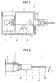
- FIG. 1 is a schematic cross-sectional view of a semiconductor laser module according to a first embodiment of the present invention viewed from the top.
- the semiconductor laser module 1 includes a housing 2 and a semiconductor device 3 that is housed in the housing 2 and outputs a laser light.
- the laser light output from the semiconductor device 3 is converted into a collimated light by a collimating lens 4 provided near an output facet of the laser light.
- the collimated light is, for example, 4% reflected and 96% transmitted at a beam splitter 5.
- the light reflected at the beam splitter 5 is incident on a power monitor PD 6 where the optical output is detected and on a wavelength monitor 8 where the optical output in a wavelength region selected by an etalon 7 is detected.
- the optical outputs detected by the power monitor PD 6 and the wavelength monitor PD 8 are used in a wavelength locking control.
- the light transmitted the beam splitter 5 is coupled to an optical fiber 11 that is a single-mode fiber via an optical isolator 9 and a focusing lens 10 and output.
- the semiconductor device 3 is disposed on a Peltier element 21 that is a temperature control element, so that the oscillation wavelength of the laser light is controlled by a temperature control of the Peltier element 21.
- the etalon 7 is disposed on a Peltier element 22 that is a temperature control element, so that the selection wavelength is controlled by a temperature control of the Peltier element 22.
- the semiconductor device 3 is a wavelength-selective-type wavelength-tunable laser shown in FIG. 2 , including a plurality of semiconductor lasers 12 arranged in an array.
- Each of the semiconductor lasers 12 is designed to have a capability of wavelength tuning by an amount of about 3 nm to 4 nm, and the oscillation wavelengths of the semiconductor lasers 12 are arranged at wavelength intervals of about 3 nm to 4 nm.
- the entirety of the C-band (1.53 ⁇ m to 1.56 ⁇ m) or the L-band (1.57 ⁇ m to 1.61 ⁇ m) by integrating 10 or more of the semiconductor lasers 12 (3 nm to 4 nm wavelength tunable), for example, it is possible to tune the wavelength over a wavelength range of 30 nm or more.
- the laser light selected and output from a semiconductor laser array 13 including the semiconductor lasers 12 is input to an optical coupler 15 through a corresponding one of a plurality of waveguides 14 and output to a waveguide 16.
- the light guided through the waveguide 16 is amplified by a semiconductor optical amplifier (SOA) 17, and is then output through a bending waveguide 18, with an inclination angle of about 7 degrees with respect to the output facet.
- the inclination angle is preferably in a range of 6 degrees to 12 degrees. With this configuration, it is possible to reduce a back-reflection light returning toward the semiconductor laser array 13.
- the bending waveguide 18 is formed with a bending radius R of 1000 ⁇ m or more to serve as a waveform shaping unit.
- FIG. 3 shows an FFP of a laser light output from the output facet when the optical output is changed in a semiconductor device of a related art in which the bending radius is 1000 ⁇ m or less, and (b) shows an FFP of a laser light output from the output facet when the optical output is changed in the semiconductor device 3 according to the first embodiment of the present invention in which the bending radius is 1000 ⁇ m or more.
- the positive and negative signs of an angle ⁇ shown in FIG. 3 are set with respect to the optical axis of the laser light shown in FIG. 2 as 0 degrees.
- the FFP of the related art shown in (a) of FIG. 3 includes a side lobe SB on the wavelength monitor PD 8 side, and the FFP changes when the optical output is changed to 10 mW, 15 mW, 20 mW, and 25 mW. In particular, the change is noticeable near the angle of 0 degrees and near the side lobe SB. In contrast, when the bending radius is set to 1000 ⁇ m or more, as shown in (b) of FIG. 3 , the FFP rarely changes even when the optical output is changed, and a stable FFP is obtained. In addition, the FFP has a Gaussian distribution that is substantially symmetrical with respect to the angle of 0 degrees.
- the leakage light I2 becomes a loss, and the efficiency of optical coupling to the optical fiber 11 changes.
- the fiber-end optical output Pf (mW) is not relatively proportional to the power monitor current value Im ( ⁇ A) detected by the power monitor PD 6.
- the efficiency of optical coupling to the optical fiber 11 is constant. As a result, as shown in FIG.
- the fiber-end optical output Pf (and the optical output of the selected semiconductor laser 12) and the power monitor current value Im have a substantially proportional relation with each other.
- the fiber-end optical output Pf (and the optical output of the selected semiconductor laser 12) and the wavelength monitor current Iwm that is the output of the wavelength monitor PD 8 are also approximately proportional to each other.
- the wavelength locking control based on the monitoring results by the power monitor PD 6 and the wavelength monitor PD 8 will be described.
- the wavelength locking control is performed as follows. First, a desired fiber-end optical output Pf, the wavelength monitor current Iwm at an oscillation wavelength ⁇ , and a ratio Iwm/Im of the wavelength monitor current Iwm to the power monitor current value are measured in advance.
- the driving current Isoa of the semiconductor optical amplifier 17 is controlled to obtain target values of the fiber-end optical output Pf and the ratio Iwm/Im, and the temperature of the semiconductor device 3 is controlled with the Peltier element 21. That is, by controlling the ratio Iwm/Im to be constant, the wavelength locking control is realized.
- the semiconductor laser module of the related art has characteristics such that the fiber-end optical output Pf is not proportional to the power monitor current value Im and the wavelength monitor current Iwm, the ratio Iwm/Im will change as shown in (a) of FIG. 6 , if the wavelength locking control is performed using these characteristics.
- the wavelength locking control since the semiconductor laser module of the related art, as shown in FIG. 5 , has characteristics such that the fiber-end optical output Pf is not proportional to the power monitor current value Im and the wavelength monitor current Iwm, the ratio Iwm/Im will change as shown in (a) of FIG. 6 , if the wavelength locking control is performed using these characteristics.
- the semiconductor laser module since the semiconductor laser module has characteristics such that the fiber-end optical output Pf is proportional to the power monitor current value Im and the wavelength monitor current Iwm (linearity), the ratio Iwm/Im does not change even when the optical power is changed. Moreover, as shown in FIG. 5 , it is possible to use the same target value P2 regardless of a change in the optical power, and the oscillation frequency (oscillation wavelength) is not shifted. Thus, it is possible to perform the wavelength locking control with a high degree of accuracy.
- the bending radius R is set to 1000 ⁇ m or more when the equivalent refractive index difference ⁇ n of the bending waveguide 18 is 1.06. This is because, as shown in FIG. 7 , if the bending radius R is 1000 ⁇ m or more, the transmittance is 98% or more, and an optical power loss PL that is assumed to result from the leakage light is 2% or less. If the optical power loss PL is maintained to be 2% or less, the FFP barely changes even when the optical output is changed.
- the relation between the bending radius R and the equivalent refractive index difference ⁇ n when the optical power loss PL is 2% is shown in FIG. 8 .
- a leakage-light blocking portion 20 that blocks a leakage light from the optical coupler 15 or the like, which serves as a waveform shaping unit, is provided halfway between the optical coupler 15 and the bending waveguide 18 of the first embodiment described above. Width this configuration, since the leakage light from the optical coupler 15 does not affect the FFP, it is possible to obtain a stable FFP.
- the leakage light from the optical coupler 15 may contain higher-order mode components, however, with the above configuration, it is possible to prevent fluctuation of the FFP due to the higher-order mode components.
- the leakage-light blocking portion 20 may be configured to block the light spatially or may be formed of a member that actively absorbs light.
- the bending waveguide 18 is not arranged at the last-stage waveguide, but is provided between the optical coupler 15 and the semiconductor optical amplifier 17. Since a waveguide 30 at the backward stage of the semiconductor optical amplifier 17 is formed to be oblique to the output facet, it is possible to suppress a back-reflection light.
- the bent portion of the bending waveguide 18, which is bent at the angle of 7 degrees, is not arranged near the output port as shown FIG. 11 , but is provided near the input port for the laser light of an output-side waveguide that includes the bending waveguide 18, the semiconductor optical amplifier 17, and the waveguide 30 as shown in FIG. 12 .
- FIG. 13 shows the FFP of the fiber-end optical output of the configuration shown in FIG. 11 .
- FIG. 14 shows the FFP of the fiber-end optical output of the configuration shown in FIG. 12 .
- the bending radius R of the bending waveguide 18 is set to 1000 ⁇ m or less.
- a region in which the curve changes nonlinearly like a bump indicated by an arrow is created on a skirt of the distribution profile.
- the structure of the present invention it is possible to obtain an ideal distribution profile as shown in FIG. 14 in which the laser light output and the detection values of the detectors have a linear relation.
- the position of the bent portion may change depending on the bending angle of the waveguide, the material properties of the waveguide, and the way the light flux of the output light is used. In many cases, favorable results can be obtained when the bent portion is designed to be located within the range of 5% to 30% of the distance between the input port and the output port of the output-side waveguide.
- the semiconductor laser module according to the present invention is suitable for use as a signal light source for optical communication, for example.
Landscapes
- Physics & Mathematics (AREA)
- General Physics & Mathematics (AREA)
- Optics & Photonics (AREA)
- Condensed Matter Physics & Semiconductors (AREA)
- Electromagnetism (AREA)
- Semiconductor Lasers (AREA)
- Optical Couplings Of Light Guides (AREA)
Abstract
Description
- The present invention relates to a semiconductor laser module in which a laser light output from a semiconductor laser element is emitted with an inclination relative to an output facet using a bending waveguide so that reflected light can be reduced.
- In order to reduce a back-reflected light from an output facet when a laser light is output from a semiconductor laser element, a bending waveguide is widely used, which bends at about 7 degrees with respect to the output facet, for example. With the help of the bending waveguide, the back-reflected light returning to a resonator of the semiconductor laser element is reduced, so that a stable laser light can be output.
- On the other hand, in a conventional semiconductor laser module in which light output from a semiconductor laser module is guided to an optical fiber to output the light through the optical fiber, a part of the output laser light is branched by a beam splitter or the like, and wavelength locking control is performed using an optical power monitor and a wavelength monitor that monitors the optical power of a predetermined wavelength. In this case, when the beam splitter is provided to each of the optical power monitor and the wavelength monitor, the number of optical components increases, which impedes downsizing of the semiconductor laser module. Therefore, a technique is disclosed in which an optical power monitor and a wavelength monitor are disposed in parallel on the light flux of the light branched by the beam splitter, and the branched light are divided in the optical axis direction to be respectively received by the optical power monitor and the wavelength monitor (see Patent Document 1).
- Patent Document 1: Japanese Patent Application Laid-Open No.
2006-216695 - However, when the bending waveguide is used, leakage light from the bending waveguide as well as guided light output in the guiding direction of an output facet is present in the laser light output from the output facet. Due to the presence of the leakage light, a far-field pattern (FFP), which is a distribution pattern of the laser light output from the output facet, is symmetrical with respect to the center of the optical axis because a side lobe appears on the leakage light side.
- If the monitoring of the optical power of light output from a semiconductor device having the bending waveguide is performed with a power monitor and a wavelength monitor using the light branched by a single beam splitter, the detected optical output power differs between the power monitor and the wavelength monitor due to the asymmetry of the FFP. Therefore, there is a problem in that it is difficult to perform the wavelength locking control with a high degree of accuracy. In particular, since the FFP changes with a change in the optical power of the laser light, and the magnitude of the difference also changes, there is a problem in that it is difficult to perform wavelength locking control with a high degree of accuracy.
- The present invention has been made in view of the above aspects, and an object of the invention is to provide a semiconductor laser module capable of performing the wavelength locking control in a stable manner with a high degree of accuracy even when monitoring the optical power and the wavelength of light, respectively using lights obtained by dividing a light output from a semiconductor device having a bending waveguide in the optical axis direction.
- To solve the problems and to attain the object, there is provided a semiconductor laser module including a semiconductor device in which at least a semiconductor laser and a bending waveguide are integrated, a beam splitter, and a plurality of detectors. A laser light emitted from the semiconductor laser propagates through the bending waveguide, the laser light output from the bending waveguide is input to the beam splitter, a part of the laser light input to the beam splitter is branched by the beam splitter, and the part of laser light branched is detected by the detectors arranged at different positions in a cross section of a light flux of the part of the laser light. The semiconductor laser module further includes a waveform shaping unit provided on an optical path for bringing a relation between an output of the semiconductor laser and detection values of the detectors close to linear.
- Furthermore, in the semiconductor laser module according to the present invention, the waveform shaping unit shapes an optical output distribution pattern to be substantially symmetrical with respect to an optical axis of the laser light.
- Moreover, in the semiconductor laser module according to the present invention, the waveform shaping unit is the bending waveguide with a bending radius of 1000 µm or more.
- Furthermore, in the semiconductor laser module according to the present invention, the waveform shaping unit satisfies

where R is bending radius of the bending waveguide and Δn is equivalent refractive index difference between a waveguide portion and a cladding portion of the bending waveguide defined as {(refractive index of waveguide portion)-(refractive index of cladding portion)}/(refractive index of waveguide portion). - Moreover, in the semiconductor laser module according to the present invention, the waveform shaping unit shapes an optical output distribution pattern such that an optical output loss by the bending waveguide is 2% or less.
- Furthermore, in the semiconductor laser module according to the present invention, the semiconductor device includes a selective-type wavelength-tunable laser including a plurality of semiconductor lasers, in which one of the semiconductor lasers is selected to output a wavelength-tunable laser light and an optical coupler that outputs the laser light emitted from the selective-type wavelength-tunable laser toward the bending waveguide, and the waveform shaping unit includes a leakage-light blocking portion that blocks a leakage light from the optical coupler.
- Moreover, in the semiconductor laser module according to the present invention, a semiconductor optical amplifier that amplifies the laser light emitted from the semiconductor laser is further integrated in the semiconductor device, and the waveform shaping unit shapes the optical output distribution pattern by providing the bending waveguide at a stage prior to an optical input stage of the semiconductor optical amplifier.
- Furthermore, in the semiconductor laser module according to the present invention, the detectors include an output detector that detects an optical output of the semiconductor device and a wavelength detector that detects an optical output in a predetermined wavelength region of the laser light output from the semiconductor device.
- Moreover, in the semiconductor laser module according to the present invention, a bent portion of the bending waveguide is set at a position in a distance of 5% to 30% of a waveguide including the bending waveguide from a laser light input port of the waveguide.
- According to the present invention, the waveform shaping unit is configured to shape the optical output distribution pattern within a plane vertical to the optical axis of the laser light into an optical output distribution pattern which does not depend on the power of the laser light, by the bending radius of the bending waveguide being 1000 µm or more or the like. Therefore, it is possible to stably perform wavelength locking control with a high degree of accuracy even in the case of detecting lights which are output from a semiconductor device having a bending waveguide and are present at different positions on the light flux.
-
-
FIG. 1 is a schematic cross-sectional view of a semiconductor laser module according to a first embodiment of the present invention viewed from the top. -
FIG. 2 is a schematic diagram showing a configuration of the semiconductor device shown inFIG. 1 . -
FIG. 3 shows an FFP of a related art and an FFP in which a bending radius is 1000 µm or more. -
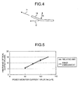
FIG. 4 is a schematic diagram showing guided light and leakage light output from a bending waveguide. -
FIG. 5 is a graph showing a dependence of a fiber-end optical output on a power monitor current value according to the related art and the first embodiment. -
FIG. 6 shows a dependence of a wavelength monitor current value/a power monitor current value on an oscillation frequency according to the related art and the first embodiment. -
FIG. 7 is a graph showing a dependence of transmittance on a bending radius. -
FIG. 8 is a graph showing a dependence of a bending radius on an equivalent refractive index difference. -
FIG. 9 is a schematic diagram showing a configuration of a semiconductor device according to a second embodiment of the present invention. -
FIG. 10 is a schematic diagram showing a configuration of a semiconductor device according to a third embodiment of the present invention. -
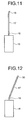
FIG. 11 is a schematic diagram showing a configuration of a semiconductor device in which a bending waveguide is provided near an output port. -
FIG. 12 is a schematic diagram showing a configuration of a semiconductor device in which a bending waveguide is provided near an input port. -
FIG. 13 is a diagram showing an FFP of optical output of a fiber-end by the semiconductor device shown inFIG. 11 . -
FIG. 14 is a diagram showing an FFP of optical output of a fiber-end by the semiconductor device shown inFIG. 12 . Description of Embodiments - Exemplary embodiments of a semiconductor laser module according to the present invention are described in detail below with reference to accompanying drawings. The present invention is not limited to these embodiments.
-
FIG. 1 is a schematic cross-sectional view of a semiconductor laser module according to a first embodiment of the present invention viewed from the top. Thesemiconductor laser module 1 includes ahousing 2 and asemiconductor device 3 that is housed in thehousing 2 and outputs a laser light. The laser light output from thesemiconductor device 3 is converted into a collimated light by acollimating lens 4 provided near an output facet of the laser light. The collimated light is, for example, 4% reflected and 96% transmitted at abeam splitter 5. - The light reflected at the
beam splitter 5 is incident on apower monitor PD 6 where the optical output is detected and on awavelength monitor 8 where the optical output in a wavelength region selected by anetalon 7 is detected. The optical outputs detected by thepower monitor PD 6 and thewavelength monitor PD 8 are used in a wavelength locking control. - On the other hand, the light transmitted the
beam splitter 5 is coupled to anoptical fiber 11 that is a single-mode fiber via anoptical isolator 9 and a focusinglens 10 and output. Thesemiconductor device 3 is disposed on aPeltier element 21 that is a temperature control element, so that the oscillation wavelength of the laser light is controlled by a temperature control of thePeltier element 21. Theetalon 7 is disposed on aPeltier element 22 that is a temperature control element, so that the selection wavelength is controlled by a temperature control of the Peltierelement 22. - The
semiconductor device 3 is a wavelength-selective-type wavelength-tunable laser shown inFIG. 2 , including a plurality ofsemiconductor lasers 12 arranged in an array. Each of thesemiconductor lasers 12 is designed to have a capability of wavelength tuning by an amount of about 3 nm to 4 nm, and the oscillation wavelengths of thesemiconductor lasers 12 are arranged at wavelength intervals of about 3 nm to 4 nm. By switching thesemiconductor lasers 12 to be driven and controlling the element temperature, it is possible to cover a continuous wavelength band broader than that covered by a single semiconductor laser. In order to cover the wavelength band of WDM optical communication, for example, the entirety of the C-band (1.53 µm to 1.56 µm) or the L-band (1.57 µm to 1.61 µm), by integrating 10 or more of the semiconductor lasers 12 (3 nm to 4 nm wavelength tunable), for example, it is possible to tune the wavelength over a wavelength range of 30 nm or more. - The laser light selected and output from a
semiconductor laser array 13 including thesemiconductor lasers 12 is input to anoptical coupler 15 through a corresponding one of a plurality ofwaveguides 14 and output to awaveguide 16. The light guided through thewaveguide 16 is amplified by a semiconductor optical amplifier (SOA) 17, and is then output through a bendingwaveguide 18, with an inclination angle of about 7 degrees with respect to the output facet. The inclination angle is preferably in a range of 6 degrees to 12 degrees. With this configuration, it is possible to reduce a back-reflection light returning toward thesemiconductor laser array 13. The bendingwaveguide 18 is formed with a bending radius R of 1000 µm or more to serve as a waveform shaping unit. An equivalent refractive index difference Δn between a waveguide portion and a cladding portion of the bending waveguide 18 (where µn={(refractive index of waveguide portion)-(refractive index of cladding portion)}/(refractive index of waveguide portion)) is 1.06. - In
FIG. 3 , (a) shows an FFP of a laser light output from the output facet when the optical output is changed in a semiconductor device of a related art in which the bending radius is 1000 µm or less, and (b) shows an FFP of a laser light output from the output facet when the optical output is changed in thesemiconductor device 3 according to the first embodiment of the present invention in which the bending radius is 1000 µm or more. The positive and negative signs of an angle θ shown inFIG. 3 are set with respect to the optical axis of the laser light shown inFIG. 2 as 0 degrees. - The FFP of the related art shown in (a) of
FIG. 3 includes a side lobe SB on thewavelength monitor PD 8 side, and the FFP changes when the optical output is changed to 10 mW, 15 mW, 20 mW, and 25 mW. In particular, the change is noticeable near the angle of 0 degrees and near the side lobe SB. In contrast, when the bending radius is set to 1000 µm or more, as shown in (b) ofFIG. 3 , the FFP rarely changes even when the optical output is changed, and a stable FFP is obtained. In addition, the FFP has a Gaussian distribution that is substantially symmetrical with respect to the angle of 0 degrees. - This is considered to be attributable to the following fact. As shown in
FIG. 4 , if the bending radius R of the bendingwaveguide 18 is less than 1000 µm, a leakage light I2 is generated due to the guided light going straight, and the side lobe SB is generated by the leakage light I2. Furthermore, the amount of the leakage light I2 changes when the output is changed. In contrast, in the first embodiment, since the bending radius R of the bendingwaveguide 18 is set to 1000 µm or more, it is possible to suppress the generation of the leakage light I2 and to allow the entire light to be output as guided light I1 which is light directed in the guiding direction at the output facet. - When the FFP changed with the change in the optical output as shown in (a) of
FIG. 3 , the leakage light I2 becomes a loss, and the efficiency of optical coupling to theoptical fiber 11 changes. As a result, as shown inFIG. 5 , the fiber-end optical output Pf (mW) is not relatively proportional to the power monitor current value Im (µA) detected by thepower monitor PD 6. On the other hand, in the first embodiment, since the leakage light I2 is suppressed, and the FFP does not change with the optical output as shown in (b) ofFIG. 3 , the efficiency of optical coupling to theoptical fiber 11 is constant. As a result, as shown inFIG. 5 , the fiber-end optical output Pf (and the optical output of the selected semiconductor laser 12) and the power monitor current value Im have a substantially proportional relation with each other. Moreover, in the first embodiment, since the FFP barely changes with the optical output, the fiber-end optical output Pf (and the optical output of the selected semiconductor laser 12) and the wavelength monitor current Iwm that is the output of thewavelength monitor PD 8 are also approximately proportional to each other. - The wavelength locking control based on the monitoring results by the
power monitor PD 6 and thewavelength monitor PD 8 will be described. The wavelength locking control is performed as follows. First, a desired fiber-end optical output Pf, the wavelength monitor current Iwm at an oscillation wavelength λ, and a ratio Iwm/Im of the wavelength monitor current Iwm to the power monitor current value are measured in advance. The driving current Isoa of the semiconductoroptical amplifier 17 is controlled to obtain target values of the fiber-end optical output Pf and the ratio Iwm/Im, and the temperature of thesemiconductor device 3 is controlled with thePeltier element 21. That is, by controlling the ratio Iwm/Im to be constant, the wavelength locking control is realized. - Since the semiconductor laser module of the related art, as shown in
FIG. 5 , has characteristics such that the fiber-end optical output Pf is not proportional to the power monitor current value Im and the wavelength monitor current Iwm, the ratio Iwm/Im will change as shown in (a) ofFIG. 6 , if the wavelength locking control is performed using these characteristics. For example, inFIG. 6 , when the optical output is changed (controlled) to Pf=6.5 mW or Pf=13 mW using the same ratio Iwm/Im as that when the fiber-end optical output Pf=17 mW as a target value P1, the oscillation frequency (oscillation wavelength) is shifted. Thus, it is not possible to maintain the wavelength locking control. - On the other hand, in the first embodiment, since the semiconductor laser module has characteristics such that the fiber-end optical output Pf is proportional to the power monitor current value Im and the wavelength monitor current Iwm (linearity), the ratio Iwm/Im does not change even when the optical power is changed. Moreover, as shown in
FIG. 5 , it is possible to use the same target value P2 regardless of a change in the optical power, and the oscillation frequency (oscillation wavelength) is not shifted. Thus, it is possible to perform the wavelength locking control with a high degree of accuracy. - In the first embodiment described above, the bending radius R is set to 1000 µm or more when the equivalent refractive index difference Δn of the bending
waveguide 18 is 1.06. This is because, as shown inFIG. 7 , if the bending radius R is 1000 µm or more, the transmittance is 98% or more, and an optical power loss PL that is assumed to result from the leakage light is 2% or less. If the optical power loss PL is maintained to be 2% or less, the FFP barely changes even when the optical output is changed. - The relation between the bending radius R and the equivalent refractive index difference Δn when the optical power loss PL is 2% is shown in
FIG. 8 . The curve shown in the figure can be expressed by
where "^" is a symbol representing exponential. Therefore, when a waveguide having a given equivalent refractive index difference Δn is used, by designing the bendingwaveguide 18 to have a bending radius equal to or greater than the bending radius R calculated by the above-mentioned expression, it is possible to perform the optical output control and the wavelength locking control with a high degree of accuracy while ensuring that the FFP barely changes with a change in the optical output. - In a second embodiment of the present invention, as shown in
FIG. 9 , a leakage-light blocking portion 20 that blocks a leakage light from theoptical coupler 15 or the like, which serves as a waveform shaping unit, is provided halfway between theoptical coupler 15 and the bendingwaveguide 18 of the first embodiment described above. Width this configuration, since the leakage light from theoptical coupler 15 does not affect the FFP, it is possible to obtain a stable FFP. In particular, the leakage light from theoptical coupler 15 may contain higher-order mode components, however, with the above configuration, it is possible to prevent fluctuation of the FFP due to the higher-order mode components. The leakage-light blocking portion 20 may be configured to block the light spatially or may be formed of a member that actively absorbs light. - In a third embodiment of the present invention, as shown in
FIG. 10 , the bendingwaveguide 18 is not arranged at the last-stage waveguide, but is provided between theoptical coupler 15 and the semiconductoroptical amplifier 17. Since awaveguide 30 at the backward stage of the semiconductoroptical amplifier 17 is formed to be oblique to the output facet, it is possible to suppress a back-reflection light. - In a fourth embodiment of the present invention, the bent portion of the bending
waveguide 18, which is bent at the angle of 7 degrees, is not arranged near the output port as shownFIG. 11 , but is provided near the input port for the laser light of an output-side waveguide that includes the bendingwaveguide 18, the semiconductoroptical amplifier 17, and thewaveguide 30 as shown inFIG. 12 .FIG. 13 shows the FFP of the fiber-end optical output of the configuration shown inFIG. 11 .FIG. 14 shows the FFP of the fiber-end optical output of the configuration shown inFIG. 12 . InFIGS. 13 and 14 , the bending radius R of the bendingwaveguide 18 is set to 1000 µm or less. According to the related-art structure, a region in which the curve changes nonlinearly like a bump indicated by an arrow is created on a skirt of the distribution profile. However, according to the structure of the present invention, it is possible to obtain an ideal distribution profile as shown inFIG. 14 in which the laser light output and the detection values of the detectors have a linear relation. The position of the bent portion may change depending on the bending angle of the waveguide, the material properties of the waveguide, and the way the light flux of the output light is used. In many cases, favorable results can be obtained when the bent portion is designed to be located within the range of 5% to 30% of the distance between the input port and the output port of the output-side waveguide. - The semiconductor laser module according to the present invention is suitable for use as a signal light source for optical communication, for example.
-
- 1
- SEMICONDUCTOR LASER MODULE
- 2
- HOUSING
- 3, 23, 33
- SEMICONDUCTOR DEVICE
- 4
- COLLIMATING LENS
- 5
- BEAM SPLITTER
- 6
- POWER MONITOR PD
- 7
- ETALON
- 8
- WAVELENGTH MONITOR PD
- 9
- OPTICAL ISOLATOR
- 10
- FOCUSING LENS
- 11
- OPTICAL FIBER
- 12
- SEMICONDUCTOR LASER
- 13
- SEMICONDUCTOR LASER ARRAY
- 14, 16, 30
- WAVEGUIDE
- 15
- OPTICAL COUPLER
- 17
- SEMICONDUCTOR OPTICAL AMPLIFIER
- 18
- BENDING WAVEGUIDE
- 20
- LEAKAGE-LIGHT BLOCKING PORTION
- 21, 22
- PELTIER ELEMENT
Claims (9)
- A semiconductor laser module including a semiconductor device in which at least a semiconductor laser and a bending waveguide are integrated, a beam splitter, and a plurality of detectors, wherein a laser light emitted from the semiconductor laser propagates through the bending waveguide, the laser light output through the bending waveguide is input to the beam splitter, a part of the laser light input to the beam splitter is branched by the beam splitter, and the part of the laser light branched is detected by the detectors arranged at different positions in a cross section of a light flux of the part of the laser light, the semiconductor laser module comprising:a waveform shaping unit provided on an optical path for bringing a relation between an output of the semiconductor laser and detection values of the detectors close to linear.
- The semiconductor laser module according to claim 1, wherein the waveform shaping unit shapes an optical output distribution pattern to be substantially symmetrical with respect to an optical axis of the laser light.
- The semiconductor laser module according to claim 1 or 2, wherein the waveform shaping unit is the bending waveguide with a bending radius of 1000 µm or more.
- The semiconductor laser module according to any one of claims 1 to 3, wherein the waveform shaping unit satisfies

where R is bending radius of the bending waveguide and Δn is equivalent refractive index difference between a waveguide portion and a cladding portion of the bending waveguide defined as {(refractive index of waveguide portion)-(refractive index of cladding portion)}/(refractive index of waveguide portion). - The semiconductor laser module according to any one of claims 1 to 4, wherein the waveform shaping unit shapes an optical output distribution pattern such that an optical output loss by the bending waveguide is 2% or less.
- The semiconductor laser module according to any one of claims 1 to 5, wherein
the semiconductor device includes
a selective-type wavelength-tunable laser including a plurality of semiconductor lasers, in which one of the semiconductor lasers is selected to output a wavelength-tunable laser light, and
an optical coupler that outputs the laser light emitted from the selective-type wavelength-tunable laser toward the bending waveguide, and
the waveform shaping unit includes a leakage-light blocking portion that blocks a leakage light from the optical coupler. - The semiconductor laser module according to any one of claims 2 to 6, wherein
a semiconductor optical amplifier that amplifies the laser light emitted from the semiconductor laser is further integrated in the semiconductor device, and
the waveform shaping unit shapes the optical output distribution pattern by providing the bending waveguide at a stage prior to an optical input stage of the semiconductor optical amplifier. - The semiconductor laser module according to any one of claims 1 to 7, wherein the detectors include
an output detector that detects an optical output of the semiconductor device, and
a wavelength detector that detects an optical output in a predetermined wavelength region of the laser light output from the semiconductor device. - The semiconductor laser module according to any one of claims 1 to 8, wherein a bent portion of the bending waveguide is set at a position in a distance of 5% to 30% of a waveguide including the bending waveguide from an input port of the waveguide.
Applications Claiming Priority (2)
| Application Number | Priority Date | Filing Date | Title |
|---|---|---|---|
| JP2009077444 | 2009-03-26 | ||
| PCT/JP2010/054601 WO2010110152A1 (en) | 2009-03-26 | 2010-03-17 | Semiconductor laser module |
Publications (2)
| Publication Number | Publication Date |
|---|---|
| EP2413439A1 true EP2413439A1 (en) | 2012-02-01 |
| EP2413439A4 EP2413439A4 (en) | 2018-01-24 |
Family
ID=42780845
Family Applications (1)
| Application Number | Title | Priority Date | Filing Date |
|---|---|---|---|
| EP10755950.2A Withdrawn EP2413439A4 (en) | 2009-03-26 | 2010-03-17 | Semiconductor laser module |
Country Status (5)
| Country | Link |
|---|---|
| US (1) | US8665919B2 (en) |
| EP (1) | EP2413439A4 (en) |
| JP (1) | JPWO2010110152A1 (en) |
| CN (1) | CN102362400B (en) |
| WO (1) | WO2010110152A1 (en) |
Families Citing this family (15)
| Publication number | Priority date | Publication date | Assignee | Title |
|---|---|---|---|---|
| JPWO2013115179A1 (en) * | 2012-01-30 | 2015-05-11 | 古河電気工業株式会社 | Semiconductor optical device, integrated semiconductor optical device, and semiconductor optical device module |
| JP5567226B2 (en) | 2012-05-31 | 2014-08-06 | 古河電気工業株式会社 | Semiconductor laser module |
| JP5795126B2 (en) * | 2013-02-18 | 2015-10-14 | 古河電気工業株式会社 | Semiconductor laser device, integrated semiconductor laser device, and method of manufacturing semiconductor laser device |
| EP2816680A1 (en) | 2013-06-18 | 2014-12-24 | PBC Lasers GmbH | Laser |
| US8879601B1 (en) * | 2013-08-29 | 2014-11-04 | Ytel Photonics Inc. | Multi-wavelength laser diode module |
| JP2016018894A (en) * | 2014-07-08 | 2016-02-01 | 日本電信電話株式会社 | Integrated semiconductor optical element |
| WO2016007860A1 (en) * | 2014-07-11 | 2016-01-14 | Acacia Communications, Inc. | Integrated high-power tunable laser with adjustable outputs |
| CN106663916B (en) | 2015-02-12 | 2020-09-25 | 古河电气工业株式会社 | Semiconductor laser device |
| CN108604769B (en) * | 2016-02-12 | 2021-04-27 | 古河电气工业株式会社 | Laser module |
| CN110088997B (en) * | 2016-12-22 | 2021-06-08 | 古河电气工业株式会社 | Semiconductor Laser Module |
| JP6761390B2 (en) * | 2017-09-19 | 2020-09-23 | 日本電信電話株式会社 | Semiconductor optical integrated device |
| JP6761391B2 (en) * | 2017-09-19 | 2020-09-23 | 日本電信電話株式会社 | Semiconductor optical integrated device |
| JPWO2019111401A1 (en) * | 2017-12-08 | 2019-12-12 | 三菱電機株式会社 | Semiconductor optical device |
| US20220360047A1 (en) * | 2021-05-06 | 2022-11-10 | Microsoft Technology Licensing, Llc | Wide bandwidth laser chip |
| CN119834062B (en) * | 2024-12-30 | 2025-12-26 | 北京工业大学 | A monolithically integrated externally cooled cavity self-focusing edge-emitting laser array and its fabrication method |
Family Cites Families (13)
| Publication number | Priority date | Publication date | Assignee | Title |
|---|---|---|---|---|
| US6324204B1 (en) * | 1999-10-19 | 2001-11-27 | Sparkolor Corporation | Channel-switched tunable laser for DWDM communications |
| JP2003075666A (en) * | 2001-06-22 | 2003-03-12 | Furukawa Electric Co Ltd:The | Arrayed waveguide grating type optical multiplexer / demultiplexer |
| JP2003014963A (en) | 2001-06-27 | 2003-01-15 | Nec Corp | Semiconductor optical integrated device, method of manufacturing the same, and optical communication module |
| JP2003078209A (en) * | 2001-09-05 | 2003-03-14 | Fujitsu Ltd | Optical semiconductor device |
| JP2004055647A (en) * | 2002-07-17 | 2004-02-19 | Nec Corp | Distributed bragg reflector semiconductor laser diode, integrated semiconductor laser, semiconductor laser module, and optical network system |
| US7436867B2 (en) * | 2002-11-27 | 2008-10-14 | Intel Corporation | Hermetically sealed external cavity laser system and method |
| US7065108B2 (en) * | 2002-12-24 | 2006-06-20 | Electronics And Telecommunications Research Institute | Method of wavelength tuning in a semiconductor tunable laser |
| US7277462B2 (en) * | 2004-04-29 | 2007-10-02 | Avago Technologies Fiber (Singapore) Pte. Ltd. | Wide tuneable laser sources |
| JP2006216695A (en) | 2005-02-02 | 2006-08-17 | Furukawa Electric Co Ltd:The | Semiconductor laser module |
| JP4477572B2 (en) * | 2005-11-17 | 2010-06-09 | 古河電気工業株式会社 | Semiconductor laser module |
| JP4652995B2 (en) * | 2006-03-16 | 2011-03-16 | 古河電気工業株式会社 | Integrated semiconductor laser device and semiconductor laser module |
| JP5026776B2 (en) * | 2006-12-11 | 2012-09-19 | 株式会社リコー | Multi-beam generator, optical scanning device, and image forming apparatus |
| JP4825150B2 (en) * | 2007-02-19 | 2011-11-30 | 富士通株式会社 | Optical semiconductor integrated device and manufacturing method thereof |
-
2010
- 2010-03-17 JP JP2011506001A patent/JPWO2010110152A1/en active Pending
- 2010-03-17 US US13/203,529 patent/US8665919B2/en not_active Expired - Fee Related
- 2010-03-17 CN CN2010800134415A patent/CN102362400B/en active Active
- 2010-03-17 WO PCT/JP2010/054601 patent/WO2010110152A1/en not_active Ceased
- 2010-03-17 EP EP10755950.2A patent/EP2413439A4/en not_active Withdrawn
Non-Patent Citations (1)
| Title |
|---|
| See references of WO2010110152A1 * |
Also Published As
| Publication number | Publication date |
|---|---|
| WO2010110152A1 (en) | 2010-09-30 |
| EP2413439A4 (en) | 2018-01-24 |
| CN102362400A (en) | 2012-02-22 |
| US20110310916A1 (en) | 2011-12-22 |
| JPWO2010110152A1 (en) | 2012-09-27 |
| US8665919B2 (en) | 2014-03-04 |
| CN102362400B (en) | 2013-06-12 |
Similar Documents
| Publication | Publication Date | Title |
|---|---|---|
| US8665919B2 (en) | Semiconductor laser module | |
| US7738794B2 (en) | Optical transmitter | |
| EP2805389B1 (en) | Wavelength -tunable external cavity laser diode with a grism for oct | |
| US9722397B2 (en) | Tunable laser and tunable laser module | |
| US20100092128A1 (en) | Optical Transceiver module | |
| US20120147361A1 (en) | Wavelength monitor | |
| US6697392B2 (en) | Single wavelength laser module | |
| US10215624B2 (en) | Integrated optical tap monitor | |
| US20210405315A1 (en) | Integrated device for optically coupling a flared laser source and a waveguide | |
| CN1734287B (en) | Absolute distance measuring device | |
| JP5648391B2 (en) | Semiconductor optical device | |
| JP2013118315A (en) | Semiconductor laser device and semiconductor laser module | |
| JP7754772B2 (en) | Optical filter, wavelength-tunable laser element, wavelength-tunable laser module, and method for controlling wavelength-tunable laser module | |
| US11561206B2 (en) | Photoacoustic apparatus and methods | |
| US6327278B1 (en) | Diode laser pumped multimode waveguide laser, particularly fiber laser | |
| Grabherr et al. | Advanced single-mode VCSEL fiber pigtail | |
| CN112567578A (en) | External resonator type semiconductor laser device | |
| CN108604769A (en) | Laser module | |
| EP1796231A2 (en) | Wavelength tunable light source | |
| JP6377300B2 (en) | Wavelength monitor and optical module | |
| JP5670098B2 (en) | Semiconductor optical modulator and optical semiconductor module | |
| US20230040798A1 (en) | Optical filter, wavelength tunable laser element, wavelength tunable laser module, method of controlling wavelength tunable laser module, and computer-readable non-transitory medium | |
| JP5524821B2 (en) | Semiconductor laser module | |
| JP2016191817A (en) | OPTICAL INTEGRATED CIRCUIT AND CONTROL METHOD FOR OPTICAL INTEGRATED CIRCUIT | |
| JP2005123345A (en) | Laser emission module |
Legal Events
| Date | Code | Title | Description |
|---|---|---|---|
| PUAI | Public reference made under article 153(3) epc to a published international application that has entered the european phase |
Free format text: ORIGINAL CODE: 0009012 |
|
| 17P | Request for examination filed |
Effective date: 20110907 |
|
| AK | Designated contracting states |
Kind code of ref document: A1 Designated state(s): AT BE BG CH CY CZ DE DK EE ES FI FR GB GR HR HU IE IS IT LI LT LU LV MC MK MT NL NO PL PT RO SE SI SK SM TR |
|
| RIN1 | Information on inventor provided before grant (corrected) |
Inventor name: KIYOTA, KAZUAKI Inventor name: KIMOTO, TATSUYA |
|
| DAX | Request for extension of the european patent (deleted) | ||
| RA4 | Supplementary search report drawn up and despatched (corrected) |
Effective date: 20171222 |
|
| RIC1 | Information provided on ipc code assigned before grant |
Ipc: H01S 5/50 20060101ALI20171215BHEP Ipc: G02B 6/122 20060101ALI20171215BHEP Ipc: H01S 5/022 20060101ALI20171215BHEP Ipc: H01S 5/40 20060101ALI20171215BHEP Ipc: H01S 5/026 20060101ALN20171215BHEP Ipc: H01S 5/02 20060101AFI20171215BHEP Ipc: G02B 6/42 20060101ALI20171215BHEP Ipc: H01S 5/0683 20060101ALN20171215BHEP Ipc: G02B 6/28 20060101ALI20171215BHEP |
|
| STAA | Information on the status of an ep patent application or granted ep patent |
Free format text: STATUS: REQUEST FOR EXAMINATION WAS MADE |
|
| STAA | Information on the status of an ep patent application or granted ep patent |
Free format text: STATUS: THE APPLICATION IS DEEMED TO BE WITHDRAWN |
|
| 18D | Application deemed to be withdrawn |
Effective date: 20180720 |