EP2411996B1 - Device for generating plasma and for directing an flow of electrons towards a target - Google Patents
Device for generating plasma and for directing an flow of electrons towards a target Download PDFInfo
- Publication number
- EP2411996B1 EP2411996B1 EP10732416A EP10732416A EP2411996B1 EP 2411996 B1 EP2411996 B1 EP 2411996B1 EP 10732416 A EP10732416 A EP 10732416A EP 10732416 A EP10732416 A EP 10732416A EP 2411996 B1 EP2411996 B1 EP 2411996B1
- Authority
- EP
- European Patent Office
- Prior art keywords
- hollow element
- target
- cavity
- external
- specific material
- Prior art date
- Legal status (The legal status is an assumption and is not a legal conclusion. Google has not performed a legal analysis and makes no representation as to the accuracy of the status listed.)
- Not-in-force
Links
Images





Classifications
-
- H—ELECTRICITY
- H01—ELECTRIC ELEMENTS
- H01J—ELECTRIC DISCHARGE TUBES OR DISCHARGE LAMPS
- H01J3/00—Details of electron-optical or ion-optical arrangements common to two or more basic types of discharge tubes or lamps
- H01J3/02—Electron guns
- H01J3/025—Electron guns using a discharge in a gas or a vapour as electron source
Definitions
- the present invention concerns a device for generating plasma, an apparatus comprising such a device and a method for applying a layer of a material on a support.
- Pulsed flows of electrons are presently used for applying thin layers of specific materials on substrates. This kind of technique finds now a particularly advantageous application in the electronic field, for the production of microchips.
- the known devices A comprise a metal cathode B, which has a hollow cylindrical shape and is electrically connected to an electric feeder C; a sealed ampoule D made of dielectric material (glass and/or ceramics) and connected to the cathode B; and an auxiliary electrode E placed inside ( figure 8 ) or outside ( figure 9 ) the ampoule D.
- the devices A further comprise a capillary F, which is made of a dielectric material and protrudes from the cathode B on the opposite side with regard to the ampoule D; and an anode G, which is ring-shaped and is placed outside the cathode B, around the capillary F.
- a capillary F which is made of a dielectric material and protrudes from the cathode B on the opposite side with regard to the ampoule D
- an anode G which is ring-shaped and is placed outside the cathode B, around the capillary F.
- the cathode B is kept at a relatively high negative electric potential (namely, with a negative charge); when an electric pulse is produced on the auxiliary electrode E (e.g. by earthing said electrode), a glow discharge is created which, on its turn, generates a positive electric charge inside the cathode B.
- the positive electric charge is compensated by the emission of electrons, which are then accelerated toward the anode G inside the capillary F.
- the electrons during their motion towards the outside, ionize further molecules, thus producing further electrons (called secondary electrons).
- the electrons produced inside the cathode B and the secondary electrons are sent from the capillary G towards a target H.
- the article by NAKAGAMA ET AL (“Production of pulse high density electron beam by channel spark discharge” TRANSACTIONS OF THE INSTITUTE OF ELECTRICAL ENGINEERS OF JAPAN, PART A INST. ELECTR. ENG JAPAN, vol. 120-A, no. 4, April 2000 (2000-04), pages 391-397, XP002553605 ISSN: 0385-4205 ) discloses a device analogous to the devices described above which has, again, all the mentioned drawbacks.
- the device of the cited article comprises a brass tubular cathode fitted on a glass ampoule; and an auxiliary electrode placed inside the ampoule completely outside of the cathode.
- This device uses the so called “hollow cathode discharge” (page 11, second column, line 6); in other words, inside the ampoule a glow discharge is produced, which glow discharge has a low density of electrons.
- the aim of the present invention is to provide a device for generating plasma, an apparatus and a method for applying a layer of a material on a support, which allow to overcome, at least partially, the disadvantages of the known prior art and are, at the same time, easy and cheap to produce.
- a device for generating plasma an apparatus and a method for applying a layer of a material on a support according to what recited in the annexed independent claims and, preferably, in any one of the claims directly or indirectly dependent on the independent claims.
- Number 1 in Figure 1 indicates as a whole an apparatus for laying down a specific material.
- the apparatus 1 comprises a device 2 for generating plasma (i.e. an at least partial ionization of a rarefied gas) and for directing the flow of electrons towards a target 3, which has (in particular, is made of) the specific material, so that at least a part of the specific material is detached from the target 3 and lays down on a support 4.
- plasma i.e. an at least partial ionization of a rarefied gas
- the specific material can be formed by a single homogeneous material or by the combination of two or more different materials.
- the target 3 is earthed. In this way, the target 3 does not repel (and in fact attracts) the flow of electrons even when the electrons have already hit the target 3.
- the device 2 comprises a hollow element 5, which acts as a cathode and has (externally delimits) an internal cavity 6; and a main electrode 7, which comprises (in particular, is made of) metallic (in particular, substantially electrical conductive) material and is arranged inside the cavity 6 (delimited by the hollow element 5).
- the hollow element 5 comprises (more particularly, is made of) a metal material (more particularly, substantially electrical conductive).
- the hollow element comprises (in particular, is made of) a material selected in the group consisting of: stainless Steel, Tungsten, Molybdenum, Chrome, Iron, Titanium.
- the main electrode 7 comprises (in particular, is made of a material selected in group consisting of: stainless Steel, Tungsten, Molybdenum, Chrome, Iron, Titanium.
- the main electrode 7 extends through a wall 8 of the hollow element 5. Between the main electrode 7 and the wall 8 it is interposed a ring 9 of substantially dielectric material (in particular ceramics).
- the device 2 comprises a resistor 10 earthing the main electrode 7 and having a resistance of at least 100 Ohm, advantageously at least 1 kOhm.
- the resistor 10 has a resistance of about 20 kOhm.
- a rarefied gas is present inside the cavity 6.
- the cavity contains rarefied gas at a pressure lower than or equal to 10 -2 mbar (1 Pa).
- the rarefied gas contained inside the cavity 6 shows a pressure comprised between 10 -2 and 10 -5 mbar (1 Pa and 10 -3 Pa), specifically about 10 -3 mbar (10 -1 Pa).
- the apparatus 2 comprises a gas feed assembly (per se known and not shown) to feed an anhydrous gas (non limiting example - oxygen, nitrogen, argon, helium, xenon, etc.) inside the cavity 6; and a suction assembly (per se known and not shown) comprising a pump and able to rarefy the gas in the cavity 6 (in other words, to reduce the gas pressure inside the cavity 6).
- the feed and suction assemblies are connected to the hollow element 5 by means of a duct 23.
- the hollow element 5 is electrically connected to an activation group 11, which is able to reduce the electric potential of the hollow element 5 of at least 8 kV (in particular; starting from an electric potential substantially equal to zero) in less than 20 ns, sending an electric pulse with a charge of at least 0.16 mC to the hollow element.
- the aforesaid electric pulse is lower than or equal to 0.5 mC.
- the activation group 11 imposes a difference of potential between the hollow element 5 and the main electrode 7 according to the aforesaid parameters. As a consequence, some plasma is generated (namely an at least partial ionization of the rarefied gas) inside the cavity 6.
- the activation group 11 is able to impose on the hollow element 5 a potential decrease from 8 kV to 25 kV in less than 15 ns, in particular about 10 ns.
- the hollow element 5 is earthed. In this way, when the emission of the flow of electrons is not carried out, the hollow element is kept at a substantially null potential and the danger of spontaneous discharges between the hollow element 5 and the main electrode 7 is substantially avoided.
- a resistor 12 is connected between the hollow element 5 and the earth.
- the resistor 12 has a resistance of at least 50 kOhm.
- the resistor 12 has a resistance of at least 100 kOhm, in particular about 0.5 MOhm.
- the resistance is lower than 1 MOhm.
- the activation group 11 comprises a thyratron 13; a condenser 14, which has a frame connected to an anode 15 of the thyratron 13 and a further frame connected to the hollow element 5; and an electric feeder 16, which has a positive electrode 17 electrically connected to the anode 15 and an earthed negative electrode 18.
- the thyratron 13 has a cathode 19 which is earthed.
- the activation group 11 also comprises a control unit *20 of the thyratron 13, which control unit 20 can operate the thyratron 13 and is earthed.
- the activation group 11 comprises a magnetic compressor of the electric pulse or a Blumlein high-potential electric pulse generator.
- the magnetic compressor or the pulse generator replaces the thyratron 13 and the relative control unit 20.
- the device 2 further comprises an operator interface group (already known and therefore not illustrated), which allows an operator to adjust the operation (for instance the operation and/or the modification of working parameters) of the device 2.
- the operator interface group comprises a personal computer, a display, a keyboard and/or a pointing device (e.g. a mouse).
- the operator interface group is connected to the control unit 20.
- another electronic device having an equivalent function is used instead of the condenser 14.
- the device 2 comprises a tubular element 21, which is made of a substantially dielectric material (in particular glass) and extends through a wall 22 of the hollow element 5 opposed to the wall 8 partially inside the cavity 6 and partially inside an external chamber 24.
- the tubular element 21 has an internal lumen connecting the cavity 6 to the external chamber 24, wherein the target 3 and the supporting element 4 are placed.
- the tubular element 21 and the relative internal lumen have respective substantially circular cross sections.
- the tubular element 21 has a length from 90 mm to 220 mm.
- the tubular element has a diameter from about 5 mm to about 7 mm.
- the internal lumen of the tubular element 21 has a diameter from about 2 mm to about 4 mm.
- the other components of the device 2 have substantially proportional (with respect to the dimensions of the tubular element 21) according to what shown in figure 4 .
- the external chamber 24 is built in such a way that it is fluid-tight with regard to the external environment.
- the device 2 further comprises an external element 25, which is placed in the external chamber 24 along the tubular element 21 (i.e. not in correspondence to an end of the tubular element 21) and acts as an anode.
- the external element 25 is in contact with an external surface of the tubular element 21.
- the device 2 further comprises a potential maintenance group 26, which is electrically connected to the external element 25 to keep the electric potential of the external element 25 substantially equal to or higher than zero.
- the potential maintenance group 26 substantially earths the electric potential of the external element 25.
- the external element 25 is shaped so that it is placed around the tubular element 21; in particular, the external element 25 has a hole, through which the tubular element 21 extends. According to specific embodiments, the external element 25 is ring-shaped.
- the hollow element 5 has a substantially cylindrical shape having a substantially circular section and, advantageously, is obtained by mounting two drilled plates 28 and 29 which, once mounted, define walls 8 and 9, respectively.
- the device 2 further comprises a tube 30, which is made of a dielectric material (in particular glass or alumina), and is placed around a section of the tubular element 21 for mechanically connecting the hollow element 5 and the external element 25. Between the tube 30 and the external element 25 it is interposed a ring 31 made of a polymeric material.
- a dielectric material in particular glass or alumina
- the main electrode 7 has a web shaped end 32 made of metallic material and earthed by means of an electrical connection HV 33.
- Figures 6 and 7 show, respectively, the inside of cavity 6 and the connection between the hollow element 5 and the tubular element 21.
- the activation group 11 induces the electric pulse on the hollow element 5
- the electric potential of the external element 25 is lowered to the earth potential in about 10-20 ns.
- the hollow element 5 is in a "floating" condition for such short intervals of time. This leads to a very rapid decrease of the electric potential of the hollow element 5.
- an arc lights between an internal surface of the cavity 6 and the main electrode 7.
- the plasma of the arc expands inside the tubular element 21 and lights the discharge of the canalized spark which, on its turn, produces a high-energy flow of electrons.
- the device 2 according to the present invention can produce a particularly dense plasma and, therefore, a very intense flow of electrons (in particular, more intense than those obtainable by means of the known devices - this determines a relevant increase of the production times of thin layers).
- device 2 in accordance with the present invention is capable of producing a plasma with a density of approximately 10 17 electrons/cm 3
- the known devices such as those disclosed in WO2006/105955A2 , US2005/012441A1 and in the cited article by NAKAGAWA Y ET AL.
- the device in accordance with the present invention has, thus, an efficacy and an efficiency surprisingly higher with respect to the known devices.
- the device 1 object of the present invention does not need the presence of an ampoule connected to the hollow element 5. As a consequence, the device 1 is scarcely bulky, easy to produce and mechanically resistant.
Landscapes
- Plasma Technology (AREA)
- Physical Or Chemical Processes And Apparatus (AREA)
- Physical Vapour Deposition (AREA)
- Drying Of Semiconductors (AREA)
- Analysing Materials By The Use Of Radiation (AREA)
Description
- The present invention concerns a device for generating plasma, an apparatus comprising such a device and a method for applying a layer of a material on a support.
- Pulsed flows of electrons are presently used for applying thin layers of specific materials on substrates. This kind of technique finds now a particularly advantageous application in the electronic field, for the production of microchips.
- Different experimental systems for generating pulsed flow of electrons for producing thin layers are already known. However, as far as we know, only two systems have found an industrial application. These systems are based upon a process called Channel Spark Ablation. In these systems the flow generation occurs by extracting electrons from a plasma generated in a rarefied gas by applying a not elevated difference of potential (lower than 30 kV).
- Examples of known devices using the process of Channel Spark Ablation are illustrated in
figures 8 and9 , and are disclosed in the patent application with the publication numberWO2006/105955A2 . In particular, the known devices A comprise a metal cathode B, which has a hollow cylindrical shape and is electrically connected to an electric feeder C; a sealed ampoule D made of dielectric material (glass and/or ceramics) and connected to the cathode B; and an auxiliary electrode E placed inside (figure 8 ) or outside (figure 9 ) the ampoule D. The devices A further comprise a capillary F, which is made of a dielectric material and protrudes from the cathode B on the opposite side with regard to the ampoule D; and an anode G, which is ring-shaped and is placed outside the cathode B, around the capillary F. - In use, the cathode B is kept at a relatively high negative electric potential (namely, with a negative charge); when an electric pulse is produced on the auxiliary electrode E (e.g. by earthing said electrode), a glow discharge is created which, on its turn, generates a positive electric charge inside the cathode B. The positive electric charge is compensated by the emission of electrons, which are then accelerated toward the anode G inside the capillary F. The electrons, during their motion towards the outside, ionize further molecules, thus producing further electrons (called secondary electrons). The electrons produced inside the cathode B and the secondary electrons are sent from the capillary G towards a target H.
- The known devices of the aforesaid kind have several disadvantages, among which, for instance:
- the devices are relatively elongated, and therefore bulky, because of the presence both of the ampoule F and of the cathode B;
- the devices can be relatively easily damaged; the ampoule D is made of a dielectric material much more fragile than other components made of metallic material;
- the devices are difficult to produce; the fluid tight insertion of the auxiliary electrode E into the ampoule D is very difficult because of the fragility of the ampoule D;
- the devices emit low-density flow of electrons (the density is particularly low when the auxiliary electrode E is placed outside the ampoule D); this causes a relevant increase of the production time of thin layers;
- the devices are hardly controllable: considering that the cathode B is kept charged for long periods, it is possible the development of spontaneous discharges between the cathode B and the anode G.
- The article by NAKAGAMA ET AL ("Production of pulse high density electron beam by channel spark discharge" TRANSACTIONS OF THE INSTITUTE OF ELECTRICAL ENGINEERS OF JAPAN, PART A INST. ELECTR. ENG JAPAN, vol. 120-A, no. 4, April 2000 (2000-04), pages 391-397, XP002553605 ISSN: 0385-4205) discloses a device analogous to the devices described above which has, again, all the mentioned drawbacks. In particular, the device of the cited article comprises a brass tubular cathode fitted on a glass ampoule; and an auxiliary electrode placed inside the ampoule completely outside of the cathode. This device uses the so called "hollow cathode discharge" (
page 11, second column, line 6); in other words, inside the ampoule a glow discharge is produced, which glow discharge has a low density of electrons. - The structure, the functioning and the disadvantages of the device disclosed by the patent application having publication number
US2005/012441 are analogous to those indicated above. - The aim of the present invention is to provide a device for generating plasma, an apparatus and a method for applying a layer of a material on a support, which allow to overcome, at least partially, the disadvantages of the known prior art and are, at the same time, easy and cheap to produce.
- According to the present invention there are provided a device for generating plasma, an apparatus and a method for applying a layer of a material on a support according to what recited in the annexed independent claims and, preferably, in any one of the claims directly or indirectly dependent on the independent claims.
- The invention is hereinafter described with a reference to the annexed drawings, illustrating some non limiting embodiments, wherein:
-
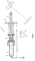
figure 1 schematically shows an apparatus and a device according to the present invention; -
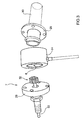
figure 2 is a perspective side view of a part of a device according to the present invention; -
figure 3 is a ,perspective view of disassembled components of the device offigure 2 ; -
figure 4 is a perspective side view of disassembled components of the device offigure 2 ; -
figure 5 is a perspective view of a component (the main electrode) of the device offigure 2 ; -
figures 6 and 7 are prospective views of opposed sides of a component (the cathode) of the device offigure 2 ; and -
figures 8 and9 show devices belonging to the prior art. -
Number 1 inFigure 1 indicates as a whole an apparatus for laying down a specific material. Theapparatus 1 comprises adevice 2 for generating plasma (i.e. an at least partial ionization of a rarefied gas) and for directing the flow of electrons towards a target 3, which has (in particular, is made of) the specific material, so that at least a part of the specific material is detached from the target 3 and lays down on a support 4. - According to alternative embodiments, the specific material can be formed by a single homogeneous material or by the combination of two or more different materials.
- Advantageously, the target 3 is earthed. In this way, the target 3 does not repel (and in fact attracts) the flow of electrons even when the electrons have already hit the target 3.
- The
device 2 comprises ahollow element 5, which acts as a cathode and has (externally delimits) aninternal cavity 6; and amain electrode 7, which comprises (in particular, is made of) metallic (in particular, substantially electrical conductive) material and is arranged inside the cavity 6 (delimited by the hollow element 5). In particular, thehollow element 5 comprises (more particularly, is made of) a metal material (more particularly, substantially electrical conductive). According to some embodiments, the hollow element comprises (in particular, is made of) a material selected in the group consisting of: stainless Steel, Tungsten, Molybdenum, Chrome, Iron, Titanium. According to some embodiments, themain electrode 7 comprises (in particular, is made of a material selected in group consisting of: stainless Steel, Tungsten, Molybdenum, Chrome, Iron, Titanium. - According to the embodiment depicted in
figure 1 , themain electrode 7 extends through awall 8 of thehollow element 5. Between themain electrode 7 and thewall 8 it is interposed aring 9 of substantially dielectric material (in particular ceramics). - Furthermore, the
device 2 comprises aresistor 10 earthing themain electrode 7 and having a resistance of at least 100 Ohm, advantageously at least 1 kOhm. In particular, theresistor 10 has a resistance of about 20 kOhm. - According to further embodiments, another electronic device having an equivalent function is used instead of the
resistor 10. - A rarefied gas is present inside the
cavity 6. According to some embodiments, the cavity contains rarefied gas at a pressure lower than or equal to 10-2 mbar (1 Pa). Advantageously, the rarefied gas contained inside thecavity 6 shows a pressure comprised between 10-2 and 10-5 mbar (1 Pa and 10-3 Pa), specifically about 10-3 mbar (10-1 Pa). - In this regard, please note that the
apparatus 2 comprises a gas feed assembly (per se known and not shown) to feed an anhydrous gas (non limiting example - oxygen, nitrogen, argon, helium, xenon, etc.) inside thecavity 6; and a suction assembly (per se known and not shown) comprising a pump and able to rarefy the gas in the cavity 6 (in other words, to reduce the gas pressure inside the cavity 6). The feed and suction assemblies are connected to thehollow element 5 by means of aduct 23. - The
hollow element 5 is electrically connected to anactivation group 11, which is able to reduce the electric potential of thehollow element 5 of at least 8 kV (in particular; starting from an electric potential substantially equal to zero) in less than 20 ns, sending an electric pulse with a charge of at least 0.16 mC to the hollow element. According to some embodiments, the aforesaid electric pulse is lower than or equal to 0.5 mC. - Therefore, in use, the
activation group 11 imposes a difference of potential between thehollow element 5 and themain electrode 7 according to the aforesaid parameters. As a consequence, some plasma is generated (namely an at least partial ionization of the rarefied gas) inside thecavity 6. - Advantageously, the
activation group 11 is able to impose on the hollow element 5 a potential decrease from 8 kV to 25 kV in less than 15 ns, in particular about 10 ns. - With a particular reference to what shown in
figure 1 , thehollow element 5 is earthed. In this way, when the emission of the flow of electrons is not carried out, the hollow element is kept at a substantially null potential and the danger of spontaneous discharges between thehollow element 5 and themain electrode 7 is substantially avoided. - In particular, a
resistor 12 is connected between thehollow element 5 and the earth. According to some embodiments, theresistor 12 has a resistance of at least 50 kOhm. Advantageously, theresistor 12 has a resistance of at least 100 kOhm, in particular about 0.5 MOhm. According to some embodiments, the resistance is lower than 1 MOhm. - According to further embodiments, another electronic device having equivalent function is used instead of the
resistor 12. - According to the embodiment shown in
figure 1 , theactivation group 11 comprises a thyratron 13; acondenser 14, which has a frame connected to ananode 15 of the thyratron 13 and a further frame connected to thehollow element 5; and anelectric feeder 16, which has apositive electrode 17 electrically connected to theanode 15 and an earthednegative electrode 18. - Furthermore, the thyratron 13 has a
cathode 19 which is earthed. - The
activation group 11 also comprises a control unit *20 of the thyratron 13, which controlunit 20 can operate the thyratron 13 and is earthed. - According to embodiments which are not shown, the
activation group 11 comprises a magnetic compressor of the electric pulse or a Blumlein high-potential electric pulse generator. Advantageously, the magnetic compressor (or the pulse generator) replaces the thyratron 13 and therelative control unit 20. - The
device 2 further comprises an operator interface group (already known and therefore not illustrated), which allows an operator to adjust the operation (for instance the operation and/or the modification of working parameters) of thedevice 2. In particular, the operator interface group comprises a personal computer, a display, a keyboard and/or a pointing device (e.g. a mouse). The operator interface group is connected to thecontrol unit 20. - According to further embodiments, another electronic device having an equivalent function is used instead of the
condenser 14. - Moreover, the
device 2 comprises atubular element 21, which is made of a substantially dielectric material (in particular glass) and extends through awall 22 of thehollow element 5 opposed to thewall 8 partially inside thecavity 6 and partially inside anexternal chamber 24. Thetubular element 21 has an internal lumen connecting thecavity 6 to theexternal chamber 24, wherein the target 3 and the supporting element 4 are placed. Thetubular element 21 and the relative internal lumen have respective substantially circular cross sections. - According to specific embodiments, the
tubular element 21 has a length from 90 mm to 220 mm. The tubular element has a diameter from about 5 mm to about 7 mm. The internal lumen of thetubular element 21 has a diameter from about 2 mm to about 4 mm. the other components of thedevice 2 have substantially proportional (with respect to the dimensions of the tubular element 21) according to what shown infigure 4 . - The
external chamber 24 is built in such a way that it is fluid-tight with regard to the external environment. - The
device 2 further comprises anexternal element 25, which is placed in theexternal chamber 24 along the tubular element 21 (i.e. not in correspondence to an end of the tubular element 21) and acts as an anode. In particular, theexternal element 25 is in contact with an external surface of thetubular element 21. - In use, when electrons formed inside the
cavity 6 enter thetubular element 21, the difference of potential established with theexternal element 25 allows the electrons to be accelerated along thetubular element 21 towards the target 3. During their motion, these electrons hit further gas molecules and therefore determine the emission of secondary electrons which, on their turn, are accelerated towards the target 3. - The
device 2 further comprises apotential maintenance group 26, which is electrically connected to theexternal element 25 to keep the electric potential of theexternal element 25 substantially equal to or higher than zero. In particular, thepotential maintenance group 26 substantially earths the electric potential of theexternal element 25. - The
external element 25 is shaped so that it is placed around thetubular element 21; in particular, theexternal element 25 has a hole, through which thetubular element 21 extends. According to specific embodiments, theexternal element 25 is ring-shaped. - With a particular reference to
figures 2 ,3 and4 , thehollow element 5 has a substantially cylindrical shape having a substantially circular section and, advantageously, is obtained by mounting two drilledplates walls - With a reference to
figures 2 ,3 and4 , thedevice 2 further comprises atube 30, which is made of a dielectric material (in particular glass or alumina), and is placed around a section of thetubular element 21 for mechanically connecting thehollow element 5 and theexternal element 25. Between thetube 30 and theexternal element 25 it is interposed aring 31 made of a polymeric material. - With a reference to
figures 3 ,4 and5 , themain electrode 7 has a web shapedend 32 made of metallic material and earthed by means of anelectrical connection HV 33. -
Figures 6 and 7 show, respectively, the inside ofcavity 6 and the connection between thehollow element 5 and thetubular element 21. - It is important to point out that the different components of the
device 2 are tightly connected to each other by interposing suitable gaskets. - In use, when the
activation group 11 induces the electric pulse on thehollow element 5, the electric potential of theexternal element 25 is lowered to the earth potential in about 10-20 ns. Thehollow element 5 is in a "floating" condition for such short intervals of time. This leads to a very rapid decrease of the electric potential of thehollow element 5. - As a consequence, an arc lights between an internal surface of the
cavity 6 and themain electrode 7. The plasma of the arc expands inside thetubular element 21 and lights the discharge of the canalized spark which, on its turn, produces a high-energy flow of electrons. - It is important to remark that it can be experimentally observed that the
device 2 according to the present invention can produce a particularly dense plasma and, therefore, a very intense flow of electrons (in particular, more intense than those obtainable by means of the known devices - this determines a relevant increase of the production times of thin layers). In particular, it has been experimentally observed thatdevice 2 in accordance with the present invention is capable of producing a plasma with a density of approximately 1017 electrons/cm3, whereas, on the other hand, the known devices (such as those disclosed inWO2006/105955A2 ,US2005/012441A1 and in the cited article by NAKAGAWA Y ET AL.) produce a plasma with a density of about 109 electrons/cm3. - The device in accordance with the present invention has, thus, an efficacy and an efficiency surprisingly higher with respect to the known devices.
- In particular, it has been experimentally observed that at the beginning of the process a high-energy electron pulse having a duration of about 50 ns is generated (controlled by the acceleration voltage or by the charging voltage of condensers). The thus produced electrons are led and sent by means of the
tubular element 21 towards the target 3. At this point, the electric current between thehollow element 5 and the target 3 disappears, then increasing again as a consequence of the short circuit created between thehollow element 5 and the target 3 by means of a plasma column developing in the meanwhile in thetubular element 21. - Note that the
device 1 object of the present invention does not need the presence of an ampoule connected to thehollow element 5. As a consequence, thedevice 1 is scarcely bulky, easy to produce and mechanically resistant. - Unless the contrary is explicitly indicated, the content of the references (articles, books, patent applications etc.) cited in this text is herein completely recalled.
Claims (16)
- Device for generating plasma and for directing an flow of electrons towards a target (3); the device (1) comprising a hollow element (5) which has a cavity (6) and is designed to act as a cathode; a main electrode (7); a substantially dielectric tubular element (21), which extends through a wall (22) of the hollow element (5) from the cavity (6) to an external chamber (24); and an external element (25) which is designed to act as an anode, is externally placed with regard to the hollow element (5) and is exterior to and along the tubular element (21);
the device (1) being characterized in that it comprises an activation group (11) which is electrically connected to the hollow element (5) and is arranged for reducing, in operation, the electric potential of the hollow element (5) of at least 8 kV in less than 20 ns; the main electrode (7) is at least partially placed inside the cavity (6) of the hollow element (5). - Device according to Claim 1, wherein the hollow element (5) comprises a metal material substantially conductive.
- Device according to Claim 1 or 2, and comprising first resistive means (10) electrically earthing the main electrode (7).
- Device according to Claim 3, wherein the first resistive means (10) have a resistance higher than 100 Ohm.
- Device according to any one of the preceding Claims, wherein the cavity (6) contains rarefied gas at a pressure lower than or equal to 10-2 mbar (1 Pa).
- Device according to Claim 3, wherein the rarefied gas contained inside the cavity (6) has a pressure from 10-2mbar (1 Pa) to 10-5 mbar (10-3 Pa).
- Device according to any one of the preceding Claims, and comprising a potential maintenance group (26), which is electrically connected to the external element (25) and is able to keep the electric potential of the external element (25) substantially equal to or higher than zero.
- Device according Claim 7, wherein the potential maintenance group (26) earths the electric potential of the external element (25).
- Device according to one of the preceding Claims, wherein the external element (25) is shaped so that it is placed around the tubular element (21).
- Device according to any one of the preceding Claims, wherein the activation group (11) can emit an electric pulse with a global charge comprised between 0.16 mC and 0.5 mC in order to reduce the electric potential of the hollow element (5) of at least 8 kV in less than 20 ns.
- Device according to any one of the preceding Claims, wherein the activation group (11) comprises a thyratron (13).
- Device according to Claim 11, wherein the activation group (11) comprises capacitive means (14) which are electrically connected to the one side to an anode (15) of the thyratron (13) and to the other side to the hollow element (5); and an electric feeder (16), which has a positive electrode (17) electrically connected to the anode (15) of the thyratron (13).
- Device according to any one of the preceding Claims, and further comprising second resistive means (12), which have a resistance of at least 50 kOhm and are electrically connected between the hollow element (5) and the earth.
- Device according to any one of Claims 1 to 11, wherein the activation group (11) comprises a magnetic pulse compressor or a Blumlein electric pulse generator.
- Apparatus for applying on a substrate (4) a specific material, the apparatus comprising an external chamber (24), a target (3) made of a specific material and placed in the external chamber (24);
the apparatus (1) being characterized in that it comprises a device (2) as defined in one of the preceding Claims, the cavity (6) of the device and the external chamber (24) communicating and containing gas at a pressure lower than 10-2 mbar (1 Pa); the device (2) being able to direct a flow of electrons against the target (3) so that at least a part of the specific material is removed from the target (3) and settles on the support (4). - Method of applying a specific material on a support (4), the method comprising an emission step, during which a device (1) according to one of Claims from 1 to 13 directs a flow of electrons against a target (3) with the specific material in order to remove at least a part of the specific material from the target (3) and to direct it towards the support (4).
Applications Claiming Priority (3)
| Application Number | Priority Date | Filing Date | Title |
|---|---|---|---|
| ITBO2009A000167A IT1395701B1 (en) | 2009-03-23 | 2009-03-23 | DEVICE FOR PLASMA GENERATION AND TO MANAGE A FLOW OF ELECTRONS TOWARDS A TARGET |
| US18181509P | 2009-05-28 | 2009-05-28 | |
| PCT/IB2010/000644 WO2010109297A2 (en) | 2009-03-23 | 2010-03-23 | Device for generating plasma and for directing an flow of electrons towards a target |
Publications (2)
| Publication Number | Publication Date |
|---|---|
| EP2411996A2 EP2411996A2 (en) | 2012-02-01 |
| EP2411996B1 true EP2411996B1 (en) | 2013-03-13 |
Family
ID=41214865
Family Applications (1)
| Application Number | Title | Priority Date | Filing Date |
|---|---|---|---|
| EP10732416A Not-in-force EP2411996B1 (en) | 2009-03-23 | 2010-03-23 | Device for generating plasma and for directing an flow of electrons towards a target |
Country Status (6)
| Country | Link |
|---|---|
| US (1) | US8803425B2 (en) |
| EP (1) | EP2411996B1 (en) |
| JP (1) | JP2012521627A (en) |
| CN (1) | CN102449721B (en) |
| IT (1) | IT1395701B1 (en) |
| WO (1) | WO2010109297A2 (en) |
Families Citing this family (8)
| Publication number | Priority date | Publication date | Assignee | Title |
|---|---|---|---|---|
| IT1401417B1 (en) * | 2010-08-23 | 2013-07-26 | Organic Spintronics S R L | DEVICE FOR PLASMA GENERATION AND TO MANAGE A FLOW OF ELECTRONS TOWARDS A TARGET |
| US10388943B2 (en) | 2010-12-22 | 2019-08-20 | Enevate Corporation | Methods of reducing occurrences of short circuits and/or lithium plating in batteries |
| RU2462009C1 (en) * | 2011-06-08 | 2012-09-20 | Мурадин Абубекирович Кумахов | Method of changing direction of beam of accelerated charged particles, device for realising said method, electromagnetic radiation source, linear and cyclic charged particle accelerators, collider and means of producing magnetic field generated by current of accelerated charged particles |
| ITBO20110669A1 (en) * | 2011-11-23 | 2013-05-24 | Organic Spintronics S R L | METHOD FOR THE DEPOSITION OF A LAYER OF A MATERIAL ON A SUBSTRATE |
| ITBO20120320A1 (en) | 2012-06-11 | 2013-12-12 | Libuse Skocdopolova | AN APPARATUS AND A METHOD FOR THE GRENERATION OF ELECTRON AND PLASMA FROM A GAS JET |
| ITBO20120695A1 (en) | 2012-12-20 | 2014-06-21 | Organic Spintronics S R L | IMPULSED PLASMA DEPOSITION DEVICE |
| GB2528141B (en) | 2014-09-18 | 2016-10-05 | Plasma App Ltd | Virtual cathode deposition (VCD) for thin film manufacturing |
| RU2754347C1 (en) * | 2020-06-15 | 2021-09-01 | Акционерное Общество "Нииэфа Им. Д.В. Ефремова" | Source of pulse electronic beams |
Family Cites Families (11)
| Publication number | Priority date | Publication date | Assignee | Title |
|---|---|---|---|---|
| NL9001496A (en) * | 1990-06-29 | 1992-01-16 | Nl Laser Res | DEVICE FOR EXCITING A GAS DISCHARGE LASER, AND PULSE COMPRESSION DEVICE FOR USE IN SUCH EXCITATION DEVICE. |
| DE4208764C2 (en) | 1992-03-19 | 1994-02-24 | Kernforschungsz Karlsruhe | Gas filled particle accelerator |
| US5302881A (en) * | 1992-06-08 | 1994-04-12 | The United States Of America As Represented By The Secretary Of The Air Force | High energy cathode device with elongated operating cycle time |
| DE19541510C2 (en) * | 1995-11-08 | 1999-08-12 | Karlsruhe Forschzent | Pulsed electron beam source and its use |
| US5917286A (en) * | 1996-05-08 | 1999-06-29 | Advanced Energy Industries, Inc. | Pulsed direct current power supply configurations for generating plasmas |
| US6066901A (en) * | 1998-09-17 | 2000-05-23 | First Point Scientific, Inc. | Modulator for generating high voltage pulses |
| DE19849894C1 (en) * | 1998-10-29 | 2000-06-29 | Karlsruhe Forschzent | Pulsed plasma source for a gas-filled particle accelerator |
| DE10207835C1 (en) * | 2002-02-25 | 2003-06-12 | Karlsruhe Forschzent | Channel spark source for a stable electron beam e.g. an electron gun, has a conical sleeve in the hollow cathode with a gas feed and an adjusted pressure drop to give a large number of shots without loss of beam quality |
| ITMI20040008A1 (en) * | 2004-01-08 | 2004-04-08 | Valentin Dediu | SINGLE WALL CARBON NANOTUBE PRODUCTION PROCESS |
| ITMI20050585A1 (en) * | 2005-04-07 | 2006-10-08 | Francesco Cino Matacotta | APPARATUS AND PROCESS FOR GENERATION ACCELERATION AND PROPAGATION OF BANDS OF ELECTRONS AND PLASMA |
| US7589473B2 (en) * | 2007-08-06 | 2009-09-15 | Plasma Surgical Investments, Ltd. | Pulsed plasma device and method for generating pulsed plasma |
-
2009
- 2009-03-23 IT ITBO2009A000167A patent/IT1395701B1/en active
-
2010
- 2010-03-23 WO PCT/IB2010/000644 patent/WO2010109297A2/en not_active Ceased
- 2010-03-23 JP JP2012501403A patent/JP2012521627A/en active Pending
- 2010-03-23 EP EP10732416A patent/EP2411996B1/en not_active Not-in-force
- 2010-03-23 CN CN201080022641.7A patent/CN102449721B/en not_active Expired - Fee Related
- 2010-03-23 US US13/259,953 patent/US8803425B2/en not_active Expired - Fee Related
Also Published As
| Publication number | Publication date |
|---|---|
| WO2010109297A3 (en) | 2010-11-25 |
| CN102449721B (en) | 2014-12-03 |
| US8803425B2 (en) | 2014-08-12 |
| ITBO20090167A1 (en) | 2010-09-24 |
| US20120081006A1 (en) | 2012-04-05 |
| JP2012521627A (en) | 2012-09-13 |
| IT1395701B1 (en) | 2012-10-19 |
| CN102449721A (en) | 2012-05-09 |
| WO2010109297A2 (en) | 2010-09-30 |
| EP2411996A2 (en) | 2012-02-01 |
Similar Documents
| Publication | Publication Date | Title |
|---|---|---|
| US8803425B2 (en) | Device for generating plasma and for directing an flow of electrons towards a target | |
| US11690161B2 (en) | Hollow cathode apparatus | |
| Oks et al. | Development of plasma cathode electron guns | |
| EP1867221B1 (en) | Apparatus and process for generating, accelerating and propagating beams of electrons and plasma | |
| US8735766B2 (en) | Cathode assembly and method for pulsed plasma generation | |
| JP2006114450A (en) | Plasma generating device | |
| KR102268021B1 (en) | Virtual cathode deposition(vcd) for thin film manufacturing | |
| CA2695902C (en) | Cathode assembly and method for pulsed plasma generation | |
| US7214949B2 (en) | Ion generation by the temporal control of gaseous dielectric breakdown | |
| Kazakov et al. | Influence of electron beam generation on the parameters and emission characteristics of a constricted arc discharge in a pulsed forevacuum plasma-cathode electron source | |
| KR20030081060A (en) | High-frequency electron source, in particular a neutralizer | |
| EP1418796A3 (en) | Erosion reduction for EUV laser produced plasma target sources | |
| WO2002019379A1 (en) | Device and process for producing dc glow discharge | |
| US8545764B2 (en) | Microplasma array | |
| WO2012025947A1 (en) | Device for generating plasma and for directing a flow of electrons towards a target | |
| CN104364873A (en) | Device for generating plasma and directing an electron beam towards a target | |
| Kazakov et al. | Emission characteristics of a forevacuum plasma-cathode source of wide-aperture pulsed electron beam with layer (mesh) stabilization of emission plasma | |
| Becker | 25 years of microplasma science and applications: A status report | |
| US20150345021A1 (en) | Pulsed plasma deposition device | |
| RU2237942C1 (en) | Heavy-current electron gun | |
| RU2008112458A (en) | DEVICE FOR THE GENERATION OF PULSE BEAMS OF FAST ELECTRONS IN THE AIR SPACE OF THE ATMOSPHERIC PRESSURE | |
| RU2454046C1 (en) | Plasma electron emitter | |
| Bochkov et al. | Sealed-off pseudospark switches (current status and prospects) | |
| RU2654493C1 (en) | Vacuum arrester | |
| US20030151341A1 (en) | Electron source |
Legal Events
| Date | Code | Title | Description |
|---|---|---|---|
| PUAI | Public reference made under article 153(3) epc to a published international application that has entered the european phase |
Free format text: ORIGINAL CODE: 0009012 |
|
| 17P | Request for examination filed |
Effective date: 20111022 |
|
| AK | Designated contracting states |
Kind code of ref document: A2 Designated state(s): AT BE BG CH CY CZ DE DK EE ES FI FR GB GR HR HU IE IS IT LI LT LU LV MC MK MT NL NO PL PT RO SE SI SK SM TR |
|
| DAX | Request for extension of the european patent (deleted) | ||
| GRAP | Despatch of communication of intention to grant a patent |
Free format text: ORIGINAL CODE: EPIDOSNIGR1 |
|
| GRAS | Grant fee paid |
Free format text: ORIGINAL CODE: EPIDOSNIGR3 |
|
| GRAA | (expected) grant |
Free format text: ORIGINAL CODE: 0009210 |
|
| AK | Designated contracting states |
Kind code of ref document: B1 Designated state(s): AT BE BG CH CY CZ DE DK EE ES FI FR GB GR HR HU IE IS IT LI LT LU LV MC MK MT NL NO PL PT RO SE SI SK SM TR |
|
| REG | Reference to a national code |
Ref country code: GB Ref legal event code: FG4D |
|
| REG | Reference to a national code |
Ref country code: AT Ref legal event code: REF Ref document number: 601244 Country of ref document: AT Kind code of ref document: T Effective date: 20130315 Ref country code: CH Ref legal event code: EP |
|
| REG | Reference to a national code |
Ref country code: IE Ref legal event code: FG4D |
|
| REG | Reference to a national code |
Ref country code: DE Ref legal event code: R096 Ref document number: 602010005492 Country of ref document: DE Effective date: 20130508 |
|
| PG25 | Lapsed in a contracting state [announced via postgrant information from national office to epo] |
Ref country code: SE Free format text: LAPSE BECAUSE OF FAILURE TO SUBMIT A TRANSLATION OF THE DESCRIPTION OR TO PAY THE FEE WITHIN THE PRESCRIBED TIME-LIMIT Effective date: 20130313 Ref country code: NO Free format text: LAPSE BECAUSE OF FAILURE TO SUBMIT A TRANSLATION OF THE DESCRIPTION OR TO PAY THE FEE WITHIN THE PRESCRIBED TIME-LIMIT Effective date: 20130613 Ref country code: ES Free format text: LAPSE BECAUSE OF FAILURE TO SUBMIT A TRANSLATION OF THE DESCRIPTION OR TO PAY THE FEE WITHIN THE PRESCRIBED TIME-LIMIT Effective date: 20130624 Ref country code: LT Free format text: LAPSE BECAUSE OF FAILURE TO SUBMIT A TRANSLATION OF THE DESCRIPTION OR TO PAY THE FEE WITHIN THE PRESCRIBED TIME-LIMIT Effective date: 20130313 Ref country code: BG Free format text: LAPSE BECAUSE OF FAILURE TO SUBMIT A TRANSLATION OF THE DESCRIPTION OR TO PAY THE FEE WITHIN THE PRESCRIBED TIME-LIMIT Effective date: 20130613 |
|
| REG | Reference to a national code |
Ref country code: AT Ref legal event code: MK05 Ref document number: 601244 Country of ref document: AT Kind code of ref document: T Effective date: 20130313 |
|
| REG | Reference to a national code |
Ref country code: NL Ref legal event code: VDEP Effective date: 20130313 |
|
| REG | Reference to a national code |
Ref country code: LT Ref legal event code: MG4D |
|
| PG25 | Lapsed in a contracting state [announced via postgrant information from national office to epo] |
Ref country code: LV Free format text: LAPSE BECAUSE OF FAILURE TO SUBMIT A TRANSLATION OF THE DESCRIPTION OR TO PAY THE FEE WITHIN THE PRESCRIBED TIME-LIMIT Effective date: 20130313 Ref country code: GR Free format text: LAPSE BECAUSE OF FAILURE TO SUBMIT A TRANSLATION OF THE DESCRIPTION OR TO PAY THE FEE WITHIN THE PRESCRIBED TIME-LIMIT Effective date: 20130614 Ref country code: SI Free format text: LAPSE BECAUSE OF FAILURE TO SUBMIT A TRANSLATION OF THE DESCRIPTION OR TO PAY THE FEE WITHIN THE PRESCRIBED TIME-LIMIT Effective date: 20130313 Ref country code: FI Free format text: LAPSE BECAUSE OF FAILURE TO SUBMIT A TRANSLATION OF THE DESCRIPTION OR TO PAY THE FEE WITHIN THE PRESCRIBED TIME-LIMIT Effective date: 20130313 |
|
| PG25 | Lapsed in a contracting state [announced via postgrant information from national office to epo] |
Ref country code: HR Free format text: LAPSE BECAUSE OF FAILURE TO SUBMIT A TRANSLATION OF THE DESCRIPTION OR TO PAY THE FEE WITHIN THE PRESCRIBED TIME-LIMIT Effective date: 20130313 Ref country code: BE Free format text: LAPSE BECAUSE OF FAILURE TO SUBMIT A TRANSLATION OF THE DESCRIPTION OR TO PAY THE FEE WITHIN THE PRESCRIBED TIME-LIMIT Effective date: 20130313 |
|
| PG25 | Lapsed in a contracting state [announced via postgrant information from national office to epo] |
Ref country code: PT Free format text: LAPSE BECAUSE OF FAILURE TO SUBMIT A TRANSLATION OF THE DESCRIPTION OR TO PAY THE FEE WITHIN THE PRESCRIBED TIME-LIMIT Effective date: 20130715 Ref country code: AT Free format text: LAPSE BECAUSE OF FAILURE TO SUBMIT A TRANSLATION OF THE DESCRIPTION OR TO PAY THE FEE WITHIN THE PRESCRIBED TIME-LIMIT Effective date: 20130313 Ref country code: CZ Free format text: LAPSE BECAUSE OF FAILURE TO SUBMIT A TRANSLATION OF THE DESCRIPTION OR TO PAY THE FEE WITHIN THE PRESCRIBED TIME-LIMIT Effective date: 20130313 Ref country code: EE Free format text: LAPSE BECAUSE OF FAILURE TO SUBMIT A TRANSLATION OF THE DESCRIPTION OR TO PAY THE FEE WITHIN THE PRESCRIBED TIME-LIMIT Effective date: 20130313 Ref country code: NL Free format text: LAPSE BECAUSE OF FAILURE TO SUBMIT A TRANSLATION OF THE DESCRIPTION OR TO PAY THE FEE WITHIN THE PRESCRIBED TIME-LIMIT Effective date: 20130313 Ref country code: MC Free format text: LAPSE BECAUSE OF NON-PAYMENT OF DUE FEES Effective date: 20130331 Ref country code: IS Free format text: LAPSE BECAUSE OF FAILURE TO SUBMIT A TRANSLATION OF THE DESCRIPTION OR TO PAY THE FEE WITHIN THE PRESCRIBED TIME-LIMIT Effective date: 20130713 Ref country code: SK Free format text: LAPSE BECAUSE OF FAILURE TO SUBMIT A TRANSLATION OF THE DESCRIPTION OR TO PAY THE FEE WITHIN THE PRESCRIBED TIME-LIMIT Effective date: 20130313 Ref country code: RO Free format text: LAPSE BECAUSE OF FAILURE TO SUBMIT A TRANSLATION OF THE DESCRIPTION OR TO PAY THE FEE WITHIN THE PRESCRIBED TIME-LIMIT Effective date: 20130313 |
|
| PG25 | Lapsed in a contracting state [announced via postgrant information from national office to epo] |
Ref country code: PL Free format text: LAPSE BECAUSE OF FAILURE TO SUBMIT A TRANSLATION OF THE DESCRIPTION OR TO PAY THE FEE WITHIN THE PRESCRIBED TIME-LIMIT Effective date: 20130313 |
|
| REG | Reference to a national code |
Ref country code: IE Ref legal event code: MM4A |
|
| PLBE | No opposition filed within time limit |
Free format text: ORIGINAL CODE: 0009261 |
|
| STAA | Information on the status of an ep patent application or granted ep patent |
Free format text: STATUS: NO OPPOSITION FILED WITHIN TIME LIMIT |
|
| PG25 | Lapsed in a contracting state [announced via postgrant information from national office to epo] |
Ref country code: DK Free format text: LAPSE BECAUSE OF FAILURE TO SUBMIT A TRANSLATION OF THE DESCRIPTION OR TO PAY THE FEE WITHIN THE PRESCRIBED TIME-LIMIT Effective date: 20130313 Ref country code: IE Free format text: LAPSE BECAUSE OF NON-PAYMENT OF DUE FEES Effective date: 20130323 |
|
| 26N | No opposition filed |
Effective date: 20131216 |
|
| REG | Reference to a national code |
Ref country code: DE Ref legal event code: R097 Ref document number: 602010005492 Country of ref document: DE Effective date: 20131216 |
|
| PG25 | Lapsed in a contracting state [announced via postgrant information from national office to epo] |
Ref country code: MT Free format text: LAPSE BECAUSE OF FAILURE TO SUBMIT A TRANSLATION OF THE DESCRIPTION OR TO PAY THE FEE WITHIN THE PRESCRIBED TIME-LIMIT Effective date: 20130313 |
|
| REG | Reference to a national code |
Ref country code: CH Ref legal event code: PL |
|
| PG25 | Lapsed in a contracting state [announced via postgrant information from national office to epo] |
Ref country code: CH Free format text: LAPSE BECAUSE OF NON-PAYMENT OF DUE FEES Effective date: 20140331 Ref country code: LI Free format text: LAPSE BECAUSE OF NON-PAYMENT OF DUE FEES Effective date: 20140331 |
|
| PG25 | Lapsed in a contracting state [announced via postgrant information from national office to epo] |
Ref country code: SM Free format text: LAPSE BECAUSE OF FAILURE TO SUBMIT A TRANSLATION OF THE DESCRIPTION OR TO PAY THE FEE WITHIN THE PRESCRIBED TIME-LIMIT Effective date: 20130313 |
|
| PG25 | Lapsed in a contracting state [announced via postgrant information from national office to epo] |
Ref country code: TR Free format text: LAPSE BECAUSE OF FAILURE TO SUBMIT A TRANSLATION OF THE DESCRIPTION OR TO PAY THE FEE WITHIN THE PRESCRIBED TIME-LIMIT Effective date: 20130313 Ref country code: CY Free format text: LAPSE BECAUSE OF FAILURE TO SUBMIT A TRANSLATION OF THE DESCRIPTION OR TO PAY THE FEE WITHIN THE PRESCRIBED TIME-LIMIT Effective date: 20130313 |
|
| PG25 | Lapsed in a contracting state [announced via postgrant information from national office to epo] |
Ref country code: HU Free format text: LAPSE BECAUSE OF FAILURE TO SUBMIT A TRANSLATION OF THE DESCRIPTION OR TO PAY THE FEE WITHIN THE PRESCRIBED TIME-LIMIT; INVALID AB INITIO Effective date: 20100323 Ref country code: MK Free format text: LAPSE BECAUSE OF FAILURE TO SUBMIT A TRANSLATION OF THE DESCRIPTION OR TO PAY THE FEE WITHIN THE PRESCRIBED TIME-LIMIT Effective date: 20130313 Ref country code: LU Free format text: LAPSE BECAUSE OF NON-PAYMENT OF DUE FEES Effective date: 20130323 |
|
| PG25 | Lapsed in a contracting state [announced via postgrant information from national office to epo] |
Ref country code: FR Free format text: LAPSE BECAUSE OF NON-PAYMENT OF DUE FEES Effective date: 20130331 |
|
| PGFP | Annual fee paid to national office [announced via postgrant information from national office to epo] |
Ref country code: GB Payment date: 20200727 Year of fee payment: 11 |
|
| GBPC | Gb: european patent ceased through non-payment of renewal fee |
Effective date: 20210323 |
|
| PG25 | Lapsed in a contracting state [announced via postgrant information from national office to epo] |
Ref country code: GB Free format text: LAPSE BECAUSE OF NON-PAYMENT OF DUE FEES Effective date: 20210323 |
|
| PGFP | Annual fee paid to national office [announced via postgrant information from national office to epo] |
Ref country code: DE Payment date: 20220329 Year of fee payment: 13 |
|
| PGFP | Annual fee paid to national office [announced via postgrant information from national office to epo] |
Ref country code: IT Payment date: 20220307 Year of fee payment: 13 |
|
| REG | Reference to a national code |
Ref country code: DE Ref legal event code: R119 Ref document number: 602010005492 Country of ref document: DE |
|
| PG25 | Lapsed in a contracting state [announced via postgrant information from national office to epo] |
Ref country code: DE Free format text: LAPSE BECAUSE OF NON-PAYMENT OF DUE FEES Effective date: 20231003 |
|
| PG25 | Lapsed in a contracting state [announced via postgrant information from national office to epo] |
Ref country code: IT Free format text: LAPSE BECAUSE OF NON-PAYMENT OF DUE FEES Effective date: 20230323 |