EP2410632A1 - Electrical power transmission system and electrical power output device - Google Patents
Electrical power transmission system and electrical power output device Download PDFInfo
- Publication number
- EP2410632A1 EP2410632A1 EP10753440A EP10753440A EP2410632A1 EP 2410632 A1 EP2410632 A1 EP 2410632A1 EP 10753440 A EP10753440 A EP 10753440A EP 10753440 A EP10753440 A EP 10753440A EP 2410632 A1 EP2410632 A1 EP 2410632A1
- Authority
- EP
- European Patent Office
- Prior art keywords
- magnetic field
- resonant
- coupling circuit
- field coupling
- electrical power
- Prior art date
- Legal status (The legal status is an assumption and is not a legal conclusion. Google has not performed a legal analysis and makes no representation as to the accuracy of the status listed.)
- Granted
Links
- 230000005540 biological transmission Effects 0.000 title claims abstract description 289
- 230000008878 coupling Effects 0.000 claims abstract description 231
- 238000010168 coupling process Methods 0.000 claims abstract description 231
- 238000005859 coupling reaction Methods 0.000 claims abstract description 231
- 238000010586 diagram Methods 0.000 description 28
- 238000005259 measurement Methods 0.000 description 22
- 230000000694 effects Effects 0.000 description 15
- 230000008859 change Effects 0.000 description 12
- 239000004065 semiconductor Substances 0.000 description 9
- 230000007423 decrease Effects 0.000 description 8
- 230000005674 electromagnetic induction Effects 0.000 description 6
- 238000000034 method Methods 0.000 description 6
- 239000000758 substrate Substances 0.000 description 6
- 238000004519 manufacturing process Methods 0.000 description 3
- 238000006073 displacement reaction Methods 0.000 description 2
- 239000003990 capacitor Substances 0.000 description 1
- 238000007796 conventional method Methods 0.000 description 1
- 230000005684 electric field Effects 0.000 description 1
- 230000006872 improvement Effects 0.000 description 1
- 238000012986 modification Methods 0.000 description 1
- 230000004048 modification Effects 0.000 description 1
Images


Classifications
-
- H—ELECTRICITY
- H02—GENERATION; CONVERSION OR DISTRIBUTION OF ELECTRIC POWER
- H02J—CIRCUIT ARRANGEMENTS OR SYSTEMS FOR SUPPLYING OR DISTRIBUTING ELECTRIC POWER; SYSTEMS FOR STORING ELECTRIC ENERGY
- H02J50/00—Circuit arrangements or systems for wireless supply or distribution of electric power
- H02J50/50—Circuit arrangements or systems for wireless supply or distribution of electric power using additional energy repeaters between transmitting devices and receiving devices
-
- H—ELECTRICITY
- H02—GENERATION; CONVERSION OR DISTRIBUTION OF ELECTRIC POWER
- H02J—CIRCUIT ARRANGEMENTS OR SYSTEMS FOR SUPPLYING OR DISTRIBUTING ELECTRIC POWER; SYSTEMS FOR STORING ELECTRIC ENERGY
- H02J50/00—Circuit arrangements or systems for wireless supply or distribution of electric power
- H02J50/10—Circuit arrangements or systems for wireless supply or distribution of electric power using inductive coupling
- H02J50/12—Circuit arrangements or systems for wireless supply or distribution of electric power using inductive coupling of the resonant type
-
- H04B5/266—
-
- H04B5/79—
-
- H—ELECTRICITY
- H01—ELECTRIC ELEMENTS
- H01F—MAGNETS; INDUCTANCES; TRANSFORMERS; SELECTION OF MATERIALS FOR THEIR MAGNETIC PROPERTIES
- H01F38/00—Adaptations of transformers or inductances for specific applications or functions
- H01F38/14—Inductive couplings
- H01F2038/143—Inductive couplings for signals
Definitions
- the present invention relates to an electrical power transmission system and an electrical power output device, and more particularly, to an electrical power transmission system and an electrical power output device which supply electrical power using magnetic field resonance.
- electrical power can be transmitted by coupling by magnetic field resonance between a resonant element installed in a power supply device that supplies electrical power and a resonant element installed in a power receiving device that receives electrical power supplied from the power supply device.
- a resonant element installed in a power supply device that supplies electrical power
- a resonant element installed in a power receiving device that receives electrical power supplied from the power supply device.
- transmission efficiency of electrical power is lowered.
- the present invention is made in light of the above problems, and it is an object of the present invention to provide an electrical power transmission system and an electrical power output device in which transmission efficiency of electrical power is improved.
- an electrical power transmission system including: a power supply device that includes a first resonant element having inductance and capacitance, and a frequency generator that generates electrical power of an electrical signal having approximately the same frequency component as a resonant frequency decided by the inductance and the capacitance and supplies the generated electrical signal to the first resonant element; a magnetic field coupling circuit that becomes coupled by magnetic field resonance with the first resonant element; and a power receiving device that includes a second resonant element that receives electrical power from the power supply device by magnetic field resonance with the magnetic field coupling circuit.
- the magnetic field coupling circuit may have approximately the same resonant frequency as the resonant frequency decided by the inductance and the capacitance of the first resonant element.
- the magnetic field coupling circuit may generate a magnetic field on approximately the same line as magnetic field directions of magnetic fields generated by the first and second resonant elements.
- the magnetic field coupling circuit may generate a magnetic field approximately in parallel to magnetic field directions of magnetic fields generated by the first and second resonant elements.
- the magnetic field coupling circuit may be positioned at a midpoint of a distance between the first and second resonant elements.
- the magnetic field coupling circuit may include a plurality of resonant elements having inductance and capacitance.
- the power receiving device may receive electrical power from the power supply device by magnetic field resonance with the first resonant element or the magnetic field coupling circuit.
- the power receiving device may receive electrical power from the power supply device by magnetic field resonance between at least one of the first resonant element and the magnetic field coupling circuit and the second resonant element.
- an electrical power output device including: a resonant element having inductance and capacitance; a frequency generator that generates electrical power of an electrical signal having approximately the same frequency component as a resonant frequency decided by the inductance and the capacitance and supplies the generated electrical signal to the resonant element; and a plurality of resonant elements having approximately the same resonant frequency as the resonant frequency of the resonant element.
- an excellent effect capable of improving transmission efficiency of electrical power in an electrical power transmission system and an electrical power output device can be obtained.
- Fig. 1 is a block diagram illustrating a configuration example of an electrical power transmission system according to a first embodiment of the present invention.
- the electrical power transmission system includes a power supply device 100, a magnetic field coupling circuit 200, and a power receiving device 300.
- the power supply device 100 supplies the power receiving device 300 with electrical power using coupling by magnetic field resonance.
- the magnetic field coupling circuit 200 is a circuit that transmits electrical power supplied from the power supply device 100 to the power receiving device 300.
- the power receiving device 300 receives electrical power from the power supply device 100 via the magnetic field coupling circuit 200 and performs a certain operation.
- the power supply device 100 includes a frequency generator 110, a driven element 120, and a resonant element 130.
- the power supply device 100 is an example of a power supply device specified in the scope of claims.
- the power receiving device 300 includes a rectifier circuit 310, a driven element 320, a resonant element 330, and a load circuit 340.
- the power receiving device 300 is an example of a power receiving device specified in the scope of claims.
- the frequency generator 110 generates an electrical signal including a predetermined frequency component.
- the frequency generator 110 generates an electrical signal including the same frequency component as a resonant frequency of the resonant element 130. That is, the frequency generator 110 generates an electrical signal as electrical power to be supplied to the power receiving device 300.
- the frequency generator 110 is implemented by a Colpitts oscillator, a Hartley oscillator, or the like.
- the frequency generator 110 outputs electrical power of the generated electrical signal to the driven element 120.
- the frequency generator 110 may generate an electrical signal including approximately the same frequency component as the resonant frequency of the resonant element 130 or may generate an electrical signal including a plurality of frequency components near the resonant frequency.
- the frequency generator 110 is an example of a frequency generator specified in the scope of claims.
- the driven element 120 is a dielectric element that is excited by the electrical signal supplied from the frequency generator 110 and transmits the electrical signal to the resonant element 130. That is, the driven element 120 couples the frequency generator 110 with the resonant element 130 by an electromagnetic induction effect.
- the driven element 120 functions to prevent an electrical signal from being reflected by performing impedance matching between the frequency generator 110 and the resonant element 130.
- the driven element 120 is implemented by a coil.
- the driven element 120 outputs the electrical signal supplied from the frequency generator 110 to the resonant element 130 by an electromagnetic induction effect.
- the resonant element 130 is a circuit that mainly generates a magnetic field based on the electrical signal output from the driven element 120.
- the resonant element 130 has inductance and capacitance.
- the resonant element 130 is strongest in magnetic field strength at the resonant frequency.
- the resonant frequency of the resonant element 130 is decided depending on the inductance L and the capacitance C of the resonant element.
- the resonant element 130 is implemented by a coil.
- capacitance between coil lines functions as capacitance.
- the coil of the resonant element 130 generates the magnetic field in an axial direction of the coil.
- the resonant element 130 is an example of a first resonant element or an example of a resonant element of an electrical power output device, which is specified in the scope of claims.
- the magnetic field coupling circuit 200 couples the corresponding magnetic field coupling circuit 200 with the resonant element 130 of the power supply device 100 by magnetic field resonance. That is, the magnetic field coupling circuit 200 becomes coupled with the resonant element 130.
- the magnetic field coupling circuit 200 causes magnetic field coupling even between the corresponding magnetic field coupling circuit 200 and the power receiving device 300.
- the magnetic field coupling circuit 200 has inductance and capacitance.
- the magnetic field coupling circuit 200 has approximately the same resonant frequency as the resonant element 130. For example, in order to optimize a degree of coupling with the resonant element 130, the magnetic field coupling circuit 200 is set to the same resonant frequency as the resonant element 130.
- the magnetic field coupling circuit 200 is arranged between the resonant element 130 of the power supply device 100 and the resonant element 330 of the power receiving device 300.
- the magnetic field coupling circuit 200 is implemented by a coil.
- capacitance between coil lines functions as capacitance.
- the coil of the resonant element 130 generates the magnetic field in an axial direction of the coil.
- the magnetic field coupling circuit 200 transmits electrical power supplied from the power supply device 100 to the resonant element 330 by coupling by magnetic field resonance between the magnetic field coupling circuit 200 and the resonant element 330 of the power receiving device 300.
- the magnetic field coupling circuit 200 is an example of a magnetic field coupling circuit specified in the scope of claims.
- the resonant element 330 is a device receiving electrical power from the power supply device 100 according to magnetic field coupling by magnetic field resonance between the corresponding resonant element 330 and the magnetic field coupling circuit 200.
- the resonant element 330 receives electrical power from the power supply device 100 by magnetic field coupling between the corresponding resonant element 330 and the resonant element 130 of the power supply device 100.
- the resonant element 330 has inductance and capacitance.
- the resonant element 330 has approximately the same resonant frequency as the resonant element 130 or the magnetic field coupling circuit 200.
- the resonant element 330 is set to the same resonant frequency as the resonant frequency of the magnetic field coupling circuit 200.
- the resonant frequencies of the resonant element 130, the magnetic field coupling circuit 200 and the resonant element 330 are set to the same frequency.
- the resonant element 330 is implemented by a coil.
- capacitance between coil lines functions as capacitance.
- the coil of the resonant element 330 generates the magnetic field in an axial direction of the coil.
- the resonant element 330 outputs electrical power of an electrical signal generated by magnetic field coupling with the resonant element 130 to the driven element 320.
- the resonant element 330 is an example of a second resonant element specified in the scope of claims.
- the driven element 320 is a dielectric element that is excited by the electrical signal supplied from the resonant element 330 and outputs the electrical signal to the rectifier circuit 310. That is, the driven element 320 couples the resonant element 130 with the rectifier circuit 310 by an electromagnetic induction effect.
- the driven element 320 functions to prevent an electrical signal from being reflected by performing impedance matching between the resonant element 330 and the rectifier circuit 310.
- the driven element 320 is implemented by a coil.
- the driven element 320 supplies the rectifier circuit 310 with an alternating current (AC) voltage which is the electrical signal generated by an electromagnetic induction effect with the resonant element 330.
- AC alternating current
- the rectifier circuit 310 rectifies the AC voltage supplied from the driven element 320 and generates a direct current (DC) voltage as a power voltage.
- the rectifier circuit 310 supplies the load circuit 340 with the generated power voltage.
- the load circuit 340 receives the power voltage from the rectifier circuit 310 and performs a certain operation.
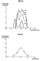
- Figs. 2A and 2B are diagrams illustrating an example of a result of measuring transmission efficiency of electrical power when the magnetic field coupling circuit 200 arranged in the middle of the transmission distance between the resonant elements 130 and 330 is rotated.
- Fig. 2A is a conceptual diagram illustrating a measurement system of transmission efficiency when the magnetic field coupling circuit 200 is rotated.
- Fig. 2B is a diagram illustrating transmission characteristics measured by the measurement system illustrated in Fig. 2A .
- Fig. 2A illustrates the driven elements 120 and 320, the resonant elements 130 and 330, and the magnetic field coupling circuit 200.
- an electrical signal applied from the frequency generator 110 to the driven element 120 is supplied to the resonant element 130 by an electromagnetic induction effect.
- the electrical signal transmitted to the resonant element 330 via the magnetic field coupling circuit 200 by magnetic field resonance with the resonant element 130 is output to the driven element 320.
- the same coils having the radius of "10 cm” are used as the resonant element 130, the magnetic field coupling circuit 200, and the resonant element 330.
- the resonant element 130, the magnetic field coupling circuit 200, and the resonant element 330 have a resonant frequency of about 26.2 MHz.
- the coils of the resonant elements 130 and 330 are arranged on the same axial line of the coils.
- the transmission distance between the resonant element 130 and 330 is "60 cm.”
- the magnetic field coupling circuit 200 is arranged at the midpoint of the transmission distance between the resonant element 130 and the resonant element 330. That is, the magnetic field coupling circuit 200 is arranged at the position of "30 cm” from the resonant element 130.
- the magnetic field coupling circuit 200 is rotated by 0°, 45°, 60°, and 90° on the midpoint of the transmission distance.
- the measurement results are illustrated in Fig. 2B .
- Fig. 2B illustrates transmission characteristics 411 to 414 and 800 between the resonant element 130 and the resonant element 330.
- a vertical axis represents an attenuation amount of electrical power in electrical power transmission between the driven elements 120 and 320, and a horizontal axis represents a frequency. The attenuation amount is based on electrical power of the electrical signal supplied from the frequency generator 110 to the driven element 120.
- the transmission characteristics 411 to 414 are transmission characteristics measured by the measurement system illustrated in Fig. 2A .
- the transmission characteristics 411 to 414 show single-peaked characteristics peaked at the resonant frequency fr.
- the transmission characteristic 411 is a transmission characteristic between the resonant element 130 and the resonant element 330 when the angle of the magnetic field coupling circuit 200 is 0°. In this case, compared to the transmission characteristics 412 to 414, the transmission characteristic 411 is smallest in attenuation amount on the resonant frequency fr.
- the transmission characteristic 412 is a transmission characteristic when the angle of the magnetic field coupling circuit 200 is 45°.
- the transmission characteristic 412 is 1 dB larger in attenuation amount of electrical power than the transmission characteristic 411.
- the transmission characteristic 413 is a transmission characteristic when the angle of the magnetic field coupling circuit 200 is 60°.
- the transmission characteristic 413 is 1 dB larger in attenuation amount of electrical power than the transmission characteristic 412.
- the transmission characteristic 414 is a transmission characteristic when the angle of the magnetic field coupling circuit 200 is 90°.
- the transmission characteristic 414 is extremely larger in attenuation amount than the transmission characteristic 413.
- the transmission characteristic 414 shows approximately the same characteristic as the transmission characteristic 800.
- the transmission characteristic 800 is a transmission characteristic when the magnetic field coupling circuit 200 is not installed between the resonant element 130 and the resonant element 330. As described above, the transmission characteristic 800 represents the same transmission characteristic as the transmission characteristic 414. For this reason, when the angle of the magnetic field coupling circuit 200 is a right angle, power transmission efficiency is hardly improved by the magnetic field coupling circuit 200.
- the attenuation amount in the transmission characteristic can be reduced compared to the transmission characteristic 800 when the magnetic field coupling circuit 200 is not installed.
- the transmission characteristic can be most improved. That is, by aligning a magnetic field direction of a magnetic field generated from the magnetic field coupling circuit 200 to be coaxial with magnetic field directions of magnetic fields generated from the resonant elements 130 and 330, the transmission efficiency between the resonant elements 130 and 330 can be improved. Further, the transmission efficiency can be improved to some extent without precisely adjusting the angle of the magnetic field coupling circuit 200.
- Fig. 3 is a conceptual diagram illustrating a measurement system of transmission efficiency when the magnetic field coupling circuit 200 moves on the same axial line between the resonant elements 130 and 330 according to the first embodiment of the present invention.
- the driven elements 120 and 320, the resonant elements 130 and 330, and the magnetic field coupling circuit 200 are illustrated.
- the driven elements 120 and 320, the resonant elements 130 and 330, and the magnetic field coupling circuit 200 are the same as ones illustrated in Fig. 2A , and thus a description thereof will be omitted.
- the transmission distance between the resonant elements 130 and 330 is "40 cm," unlike Fig. 2A .
- the magnetic field coupling circuit 200 moves between the resonant elements 130 and 330. Then, when the distance between the resonant element 130 and the magnetic field coupling circuit 200 becomes "10 cm,” “15 cm,” “20 cm,” “25 cm,” and “30 cm,” a transmission characteristic between the resonant elements 130 and 330 is measured. At this time, the coil of the magnetic field coupling circuit 200 is set to be coaxial with the coils of the resonant elements 130 and 330. The measurement results in this case are illustrated in the next drawing.
- Figs. 4A and 4B are diagrams illustrating an example of a result of measuring transmission efficiency of electrical power when the magnetic field coupling circuit 200 moves on the same axis between the resonant elements 130 and 330 according to the first embodiment of the present invention.
- Fig. 4A is a diagram illustrating transmission characteristics between the resonant elements 130 and 330 in the measurement system illustrated in Fig. 3 .
- Fig. 4B is a diagram illustrating transmission efficiency of electrical power when the magnetic field coupling circuit 200 moves on the same axis between the resonant elements 130 and 330.
- FIG. 4A transmission characteristics 421 to 425 between the resonant elements 130 and 330 are illustrated.
- a vertical axis represents an attenuation amount, and a horizontal axis represents a frequency.
- the attenuation amount is based on electrical power of the electrical signal supplied from the frequency generator 110 to the driven element 120.
- the transmission characteristics 421 to 425 are transmission characteristics measured by the measurement system illustrated in Fig. 3 .
- the transmission characteristic 421 is a transmission characteristic between the resonant element 130 and the resonant element 330 when the distance between the resonant element 130 and the magnetic field coupling circuit 200 is "10 cm.”
- the transmission characteristic 421 represents a waveform forming two peaks near 24.7 MHz and near the resonant frequency fr.
- the transmission characteristic 421 is a transmission characteristic having the largest attenuation amount compared to the transmission characteristics 422 to 425.
- the transmission characteristic 422 is a transmission characteristic when the distance between the resonant element 130 and the magnetic field coupling circuit 200 is "15 cm.”
- the transmission characteristic 422 represents a shape of three peaks near 25.3 MHz, near the resonant frequency fr, and near 27.2 MHz.
- the transmission characteristic 422 is about 7 dB smaller in attenuation amount at the resonant frequency fr than the transmission characteristic 421.
- the transmission characteristic 423 is a transmission characteristic when the distance between the resonant element 130 and the magnetic field coupling circuit 200 is "20 cm.” That is, the transmission characteristic 423 is a transmission characteristic when the magnetic field coupling circuit 200 is arranged at the midpoint of the transmission distance between the resonant elements 130 and 330.
- the transmission characteristic 423 represents a waveform forming three peaks near 25.6 MHz, near the resonant frequency fr, and near 27.0 MHz. In this case, the attenuation amount is smallest near the resonant frequency fr. That is, by installing the magnetic field coupling circuit 200 at the midpoint of the transmission distance between the resonant elements 130 and 330, the transmission efficiency becomes highest near the resonant frequency fr.
- the transmission characteristic 424 is a transmission characteristic when the distance between the resonant element 130 and the magnetic field coupling circuit 200 is "25 cm.”
- the transmission characteristic 424 represents a shape of three peaks near 25.4 MHz, near the resonant frequency fr, and near 27.1 MHz.
- the transmission characteristic 424 is about 3 dB larger in attenuation amount at the resonant frequency fr than the transmission characteristic 423.
- the transmission characteristic 425 is a transmission characteristic between the resonant element 130 and the resonant element 330 when the distance between the resonant element 130 and the magnetic field coupling circuit 200 is "30 cm.” Similarly to the transmission characteristic 421, the transmission characteristic 425 represents a waveform forming two peaks near 24.7 MHz and near the resonant frequency fr. The transmission characteristic 425 is about 8 dB larger in attenuation amount at the resonant frequency fr than the transmission characteristic 424.
- the transmission characteristic changes as the magnetic field coupling circuit 200 moves, on the same axial line of the coils of the resonant elements 130 and 330, between the resonant elements 130 and 330.
- the attenuation amount near the resonant frequency fr decreases.
- the attenuation amount near the resonant frequency fr can be minimized.
- Fig. 4B illustrates a transmission efficiency characteristic representing a relationship between the distance between the resonant element 130 and the magnetic field coupling circuit 200 and the transmission efficiency based on the attenuation amount corresponding to the resonant frequency fr illustrated in Fig. 4A .
- a vertical axis represents the transmission efficiency of electrical power between the resonant elements 130 and 330, and a horizontal axis represents the distance between the resonant element 130 and the magnetic field coupling circuit 200.
- the transmission efficiency is based on electrical power of the electrical signal supplied from the frequency generator 110 to the driven element 120.
- the transmission efficiency is highest when the distance between the resonant element 130 and the magnetic field coupling circuit 200 is "20 cm.” That is, as described above, by arranging the magnetic field coupling circuit 200 at the midpoint of the transmission distance between the resonant elements 130 and 330, the transmission efficiency of electrical power can be most improved. In this way, by arranging the resonant element 130, the magnetic field coupling circuit 200, and the resonant element 330 on the same axial line and also arranging the magnetic field coupling circuit 200 at the midpoint of the transmission distance between the resonant elements 130 and 330, the transmission efficiency can be most improved.
- Figs. 5A and 5B are diagrams illustrating a relationship between the transmission distance between the resonant elements 130 and 330 and the transmission efficiency.
- the transmission distance between the resonant elements 130 and 330 increases from “10 cm” to "80 cm,” and results of measuring the attenuation amount at the resonant frequency at intervals of "10 cm” are illustrated.
- the magnetic field coupling circuit 200 is arranged at the midpoint of the transmission distance between the resonant elements 130 and 330 so that the coils of the magnetic field coupling circuit 200 can be coaxial with the coils of the resonant elements 130 and 330.
- Fig. 5A is a diagram illustrating a relationship between the transmission distance between the resonant elements 130 and 330 and the attenuation amount.
- Fig. 5B is a diagram illustrating a relationship between the transmission distance between the resonant elements 130 and 330 and the transmission efficiency.
- a horizontal axis represents the transmission distance between the resonant elements 130 and 330.
- a transmission distance characteristic 431 is indicated by a dotted line
- a transmission distance characteristic 831 is indicated by a solid line.
- a vertical line represents the attenuation amount corresponding to the resonant frequency in electrical power transmission between the driven elements 120 and 320. The attenuation amount is based on electrical power of the electrical signal supplied from the frequency generator 110 to the driven element 120.
- the transmission distance characteristic 431 indicated by the dotted line represents a change in attenuation amount according to a transmission distance when the magnetic field coupling circuit 200 is installed at the midpoint of the transmission distance between the resonant elements 130 and 330.
- a change in attenuation amount at a transmission distance from "about 30 cm” to about “60 cm” is small. As the transmission distance increases more than "60 cm,” the attenuation amount increases.
- the transmission distance characteristic 831 indicated by the solid line represents a change in attenuation amount according to a transmission distance when the magnetic field coupling circuit 200 is not installed between the resonant elements 130 and 330.
- a change in attenuation amount at the transmission distance from “10 cm” to “30 cm” is small, but as the transmission distance increases more than "30 cm,” the attenuation amount increases.
- a degree of coupling by magnetic field resonance between the resonant elements 130 and 330 decreases according to the transmission distance between the resonant elements 130 and 330, and so the attenuation amount increases.
- the transmission distance characteristic 431 indicated by the dotted line is suppressed to a small attenuation amount, compared to the transmission distance characteristic 831 indicated by the solid line, even if the transmission distance increases. That is, by installing the magnetic field coupling circuit 200 at the midpoint of the transmission distance between the resonant elements 130 and 330, the attenuation amount by electrical power transmission between the resonant elements 130 and 330 can be suppressed.
- a transmission distance characteristic 432 is indicated by a dotted line, and a transmission distance characteristic 832 is indicated by a solid line.
- a vertical axis of the transmission distance characteristics 431 and 831 illustrated in Fig. 5A represents the transmission efficiency transformed from the attenuation amount.
- the transmission distance characteristic 432 indicated by the dotted line represents a change in transmission efficiency according to a transmission distance when the magnetic field coupling circuit 200 is installed at the midpoint of the transmission distance between the resonant elements 130 and 330.
- the transmission efficiency at a transmission distance from "about 30 cm” to about “50 cm” is about 40%, but as the transmission distance increases more than "50 cm,” the transmission efficiency decreases.
- the transmission distance characteristic 832 indicated by the solid line represents a change in transmission efficiency according to a transmission distance when the magnetic field coupling circuit 200 is not installed between the resonant elements 130 and 330.
- the amount of decrease in transmission efficiency at the transmission distance from “10 cm” to “20 cm” is small, but as the transmission distance increases more than “20 cm,” the transmission efficiency decreases. If the transmission distance is larger than "50 cm,” the transmission efficiency is lower than 10%.
- the transmission distance characteristic 432 indicated by the dotted line is suppressed to a small amount of decrease in transmission efficiency, compared to the transmission distance characteristic 832 indicated by the solid line, even if the transmission distance increases.
- the transmission efficiency is lower than 40%.
- the transmission efficiency of about 40% is maintained. For this reason, by installing the magnetic field coupling circuit 200 at the midpoint of the transmission distance between the resonant elements 130 and 330, the transmission efficiency between the resonant elements 130 and 330 can be improved.
- the transmission distance at which certain transmission efficiency can be maintained can increase.
- an example in which one magnetic field coupling circuit 200 is installed between the resonant elements 130 and 330 has been described, but a plurality of magnetic field coupling circuits may be installed. In this case, the transmission distance between the resonant elements 130 and 330 can increase.
- the transmission efficiency can be improved. Further, by installing the magnetic field coupling circuit 200 at the midpoint of the transmission distance, the transmission efficiency of electrical power can be improved except when the axis of the coil of the magnetic field coupling circuit 200 is inclined at 90° to the axis of the coils of the resonant elements 130 and 330, which is illustrated in Fig. 2 .
- Fig. 6 is a diagram illustrating a change in transmission efficiency when the axis of the coil of the magnetic field coupling circuit 200 is perpendicular to the axes of the coils of the resonant elements 130 and 330.
- the driven elements 120 and 320, the resonant elements 130 and 330, and the magnetic field coupling circuit 200 are illustrated.
- the magnetic field coupling circuit 200 moves, in the axial direction of the coil of the magnetic field coupling circuit 200, from the midpoint position of the transmission distance between the resonant elements 130 and 330.
- the transmission efficiency between the resonant elements 130 and 330 is hardly improved.
- the transmission efficiency is gradually improved.
- the distance of the magnetic field coupling circuit 200 from the midpoint position is larger than the distance of half the transmission distance between the resonant elements 130 and 330, the transmission efficiency decreases.
- the transmission efficiency in electrical power transmission between the resonant elements 130 and 330 is improved in a certain range.
- Fig. 7 is a conceptual diagram illustrating a measurement system of transmission efficiency when the magnetic field coupling circuit 200 and the resonant elements 130 and 330 are arranged so that the axes thereof can be parallel to each other according to a second embodiment of the present invention.
- the driven elements 120 and 320, the resonant elements 130 and 330, and the magnetic field coupling circuit 200 are illustrated.
- the driven elements 120 and 320, the resonant elements 130 and 330, and the magnetic field coupling circuit 200 are the same as those illustrated in Fig. 2A , and thus a description thereof will be omitted.
- the coils of the resonant element 130, the magnetic field coupling circuit 200, and the resonant element 330 are arranged so that the axes of the coils can be parallel to each other. That is, the resonant element 130, the magnetic field coupling circuit 200, and the resonant element 330 are arranged so that magnetic field directions of magnetic fields generated from the resonant element 130, the magnetic field coupling circuit 200, and the resonant element 330 can be parallel to each other.
- the transmission distance between the resonant elements 130 and 330 is "60 cm.”
- the magnetic field coupling circuit 200 moves between the resonant elements 130 and 330, and transmission characteristics when the distance between the resonant element 130 and the magnetic field coupling circuit 200 is "20 cm,” “25 cm,” “30 cm,” “35 cm,” and “40 cm” are measured.
- the coil of the magnetic field coupling circuit 200 is set to be parallel to the axes of the coils of the resonant elements 130 and 330. The measurement results in this case are illustrated in the next drawing.
- Figs. 8A and 8B are diagrams illustrating an example of a result of measuring transmission efficiency of electrical power when the magnetic field coupling circuit 200 moves between the resonant elements 130 and 330 according to the second embodiment of the present invention.
- Fig. 8A is a diagram illustrating transmission characteristics between the resonant elements 130 and 330 in the measurement system illustrated in Fig. 7 .
- Fig. 8B is a diagram illustrating transmission efficiency of electrical power when the magnetic field coupling circuit 200 moves between the resonant elements 130 and 330.
- FIG. 8A transmission characteristics 511 to 515 between the resonant elements 130 and 330 are illustrated.
- a vertical axis represents an attenuation amount in electrical power transmission between the driven elements 120 and 320, and a horizontal axis represents a frequency. The attenuation amount is based on electrical power of the electrical signal supplied from the frequency generator 110 to the driven element 120.
- the transmission characteristics 511 to 515 are transmission characteristics measured by the measurement system illustrated in Fig. 7 .
- the transmission characteristic 511 is a transmission characteristic between the resonant element 130 and the resonant element 330 when the distance between the resonant element 130 and the magnetic field coupling circuit 200 is "20 cm.”
- the transmission characteristic 511 represents a waveform forming three peaks near 23.6 MHz, near the resonant frequency fr, and near 28.0 MHz.
- the transmission characteristic 511 is a transmission characteristic having the largest attenuation amount compared to the transmission characteristics 512 to 515.
- the transmission characteristic 512 is a transmission characteristic when the distance between the resonant element 130 and the magnetic field coupling circuit 200 is "25 cm.”
- the transmission characteristic 512 represents a shape of three peaks near the resonant frequency fr and near 26.7 MHz.
- the transmission characteristic 512 is about 14 dB smaller in attenuation amount at the resonant frequency fr than the transmission characteristic 511. That is, the transmission characteristic 512 has greatly improved transmission efficiency compared to the transmission characteristic 511.
- the transmission characteristic 513 is a transmission characteristic when the distance between the resonant element 130 and the magnetic field coupling circuit 200 is "30 cm.” That is, the transmission characteristic 513 is a transmission characteristic when the magnetic field coupling circuit 200 is arranged at the midpoint of the transmission distance between the resonant elements 130 and 330.
- the transmission characteristic 513 represents a waveform forming a peak near the resonant frequency fr. In this case, the attenuation amount is smallest near the resonant frequency fr. That is, by installing the magnetic field coupling circuit 200 at the midpoint of the transmission distance between the resonant elements 130 and 330, the transmission efficiency becomes highest near the resonant frequency fr.
- the transmission characteristic 514 is a transmission characteristic when the distance between the resonant element 130 and the magnetic field coupling circuit 200 is "35 cm.” Similarly to the transmission characteristic 512, the transmission characteristic 514 represents a shape of two peaks near the resonant frequency fr and near 26.7 MHz. The transmission characteristic 514 is about 5 dB larger in attenuation amount at the resonant frequency fr than the transmission characteristic 513.
- the transmission characteristic 515 is a transmission characteristic between the resonant element 130 and the resonant element 330 when the distance between the resonant element 130 and the magnetic field coupling circuit 200 is "40 cm.”
- the transmission characteristic 515 represents a waveform forming three peaks near 24.1 MHz, near the resonant frequency fr, and 27.9 MHz.
- the transmission characteristic 515 is about 15 dB larger in attenuation amount at the resonant frequency fr than the transmission characteristic 514.
- the transmission characteristic changes as the magnetic field coupling circuit 200 moves between the resonant elements 130 and 330 in a state in which the resonant element 130, the magnetic field coupling circuit 200, and the resonant element 330 are arranged so that the axes of the coils thereof can be parallel to each other.
- the magnetic field coupling circuit 200 gets closer to the position of the midpoint of the transmission distance between the resonant elements 130 and 330, the attenuation amount near the resonant frequency fr decreases.
- the attenuation amount near the resonant frequency fr can be minimized.
- Fig. 8B illustrates a transmission efficiency characteristic representing a relationship between the distance between the resonant element 130 and the magnetic field coupling circuit 200 and the transmission efficiency based on the attenuation amount corresponding to the resonant frequency fr illustrated in Fig. 8A .
- a vertical axis represents the transmission efficiency of electrical power at the resonant frequency between the resonant elements 130 and 330, and a horizontal axis represents the distance between the resonant element 130 and the magnetic field coupling circuit 200.
- the transmission efficiency is based on electrical power of the electrical signal supplied from the frequency generator 110 to the driven element 120.
- the transmission efficiency is highest when the distance between the resonant element 130 and the magnetic field coupling circuit 200 is "30 cm.” That is, as described above, by arranging the magnetic field coupling circuit 200 at the midpoint of the transmission distance between the resonant elements 130 and 330, the transmission efficiency of electrical power can be most improved.
- the transmission efficiency can be most improved. That is, by having the resonant elements 130 and 330 to have the same magnetic field direction as the magnetic field coupling circuit 200 and arranging the magnetic field coupling circuit 200 at the midpoint of the transmission distance, the transmission efficiency can be most improved.
- the transmission efficiency can be improved. Further, in this case, by installing the magnetic field coupling circuit 200 at the midpoint of the transmission distance between the resonant elements 130 and 330, the transmission efficiency in electrical power transmission between the resonant elements 130 and 330 can be further improved. For this reason, the transmission distance between the resonant elements 130 and 330 at which certain transmission efficiency can be maintained can increase.
- magnetic field coupling circuit 200 may be arranged as described below.
- Fig. 9 is a diagram illustrating an arrangement example of the resonant element 130, the magnetic field coupling circuit 200, and the resonant element 330 according to a third embodiment of the present invention.
- the driven elements 120 and 320, the resonant elements 130 and 330, and the magnetic field coupling circuit 200 are illustrated.
- the driven elements 120 and 320, the resonant elements 130 and 330, and the magnetic field coupling circuit 200 are the same as those illustrated in Fig. 1 and are denoted by the same reference numerals, and thus a description thereof will be omitted.
- directions of the coils of the resonant element 130, the magnetic field coupling circuit 200, and the resonant element 330 are set so that the axes of the coils of the resonant element 130, the magnetic field coupling circuit 200, and the resonant element 330 can be parallel to each other.
- the resonant element 130 and the magnetic field coupling circuit 200 are arranged at a specific interval in a direction perpendicular to the axes of the coils, and the resonant element 330 is arranged in the axial direction of the coils at a predetermined interval from the midpoint of the distance between the resonant element 130 and the magnetic field coupling circuit 200.
- the power receiving device 300 receives electrical power from the power supply device 100 by magnetic field resonance with the resonant element 130 or the magnetic field coupling circuit 200.
- the magnetic field coupling circuit 200 is arranged around the resonant elements 130 and 330, since coupling by magnetic field resonance occurs between the resonant elements 130 and 330 and the magnetic field coupling circuit 200, the transmission efficiency between the resonant elements 130 and 330 can be improved. Thus, since a high efficiency area 500 in which high transmission efficiency of electrical power is obtained broadens, the resonant element 330 can receive electrical power from the resonant element 130 at a constant rate in the high efficiency area 500.
- Fig. 10 is a block diagram illustrating a configuration example of a mouse pad 710 and a mouse 720 when the first to third embodiments of the present invention are applied to the mouse pad 710 and the mouse 720.
- the mouse pad 710 that supplies electrical power and the mouse 720 that receives electrical power from the mouse pad 710 are illustrated.
- movement information representing the amount of displacement of the mouse 720 is generated, and the generated movement information is transmitted to the mouse pad 710. Then, it is assumed that the movement information is received by the mouse pad 710.
- a description will be made focusing on an arrangement of the resonant elements 130 and 330 and the magnetic field coupling circuit 200, and the remaining configuration will not be illustrated in the drawing.
- the mouse pad 710 includes the resonant element 130 and the magnetic field coupling circuit 200.
- the mouse pad 710 corresponds to the power supply device 100 illustrated in Fig. 1 .
- the mouse 720 includes the resonant element 330.
- the mouse 720 corresponds to the power receiving device 300 illustrated in Fig. 1 .
- the mouse pad 710 includes the frequency generator 110 and the driven element 120, which are illustrated in Fig. 1 .
- the mouse 720 includes the rectifier circuit 310, the driven element 220 and the load circuit 340, which are illustrated in Fig. 1 .
- the load circuit 340 measures the amount of displacement which is the movement distance and direction of the mouse 720 and generates the measured result as the movement information.
- the resonant element 130 is an element having inductance and capacitance as described above with reference to Fig. 1 .
- the resonant element 130 is implemented by a spiral coil.
- the resonant element 130 causes coupling by magnetic field resonance with the magnetic field coupling circuit 200 or the resonant element 330.
- the magnetic field coupling circuit 200 includes four resonant elements 201 to 204.
- the resonant elements 201 to 204 are elements having inductance and capacitance and are implemented by a spiral coil.
- the resonant elements 201 to 204 are on the same plane of the coil of the resonant element 130 and are arranged on diagonal lines of the resonant element 130, respectively.
- the resonant elements 201 to 204 become coupled by magnetic field resonance with the resonant element 130 or the 330.
- the resonant elements 201 to 204 have approximately the same resonant frequency as the resonant elements 130 and 330.
- the magnetic field coupling circuit 200 is an example of the magnetic field coupling circuit 200 specified in the scope of claims.
- the resonant elements 201 to 204 are an example of a plurality of resonant elements specified in the scope of claims.
- the resonant element 330 is a spiral coil having inductance and capacitance as described above with reference to Fig. 1 .
- the resonant element 330 supplies the mouse 720 with electrical power from the mouse pad 710 by coupling by magnetic field resonance with the resonant element 130 or the magnetic field coupling circuit 200.
- the mouse pad 710 is an example of an electrical power output device specified in the scope of claims.
- the first to third embodiments of the present invention may be applied to a desk and a notebook computer.
- the resonant element 130 and a plurality of resonant elements in the magnetic field coupling circuit 200 are installed inside the desk, and the resonant element 330 is installed inside the notebook computer.
- the notebook computer can receive electrical power supplied from the desk by magnetic field coupling between the resonant element 130 and the magnetic field coupling circuit 200 in the desk and the resonant element 330 in the notebook computer.
- Fig. 11 is a cross-sectional view illustrating an example of a stacking structure of a semiconductor device when the first embodiment of the present invention is applied to the semiconductor device.
- the resonant elements 130 and 330, the magnetic field coupling circuit 200, substrates 731 to 733, and metallic layers 741 to 743 are illustrated.
- the resonant element 130 and the metallic layer 741 are formed on the substrate 731 in the upper portion
- the metallic layer 742 is formed on the substrate 732 in the middle portion
- the resonant element 330 and the metallic layer 743 are formed on the substrate 733 in the lower portion.
- the resonant element 330 receives electrical power from the resonant element 130 and supplies the metallic layer 743 with the received electrical power.
- the magnetic field coupling circuit 200 on the metallic layer 742 between the resonant elements 130 and 330, the electrical power transmission efficiency between the resonant elements 130 and 330 can be improved.
- Fig. 12 is a plan view illustrating an example of the layout of a semiconductor device when the second embodiment of the present invention is applied to the semiconductor device.
- a substrate 730, the resonant elements 130 and 330, and the magnetic field coupling circuit 200 are illustrated.
- the resonant elements 130 and 330 are formed, on the substrate 730, apart from each other at a certain interval due to the manufacturing restriction.
- the electrical power transmission efficiency between the resonant elements 130 and 330 can be improved.
- the embodiments of the present invention are examples for realizing the present invention and have a correspondence relation with each of invention specifying items in the scope of claims as described above.
- the present invention is not limited to the above embodiments, and various modifications can be made in a range that does not depart from the gist of the present invention.
- the present invention can be widely applied to an electrical power transmission system, an electrical power output device, or the like which supply electrical power using magnetic field resonance.
Abstract
Description
- The present invention relates to an electrical power transmission system and an electrical power output device, and more particularly, to an electrical power transmission system and an electrical power output device which supply electrical power using magnetic field resonance.
- In the past, a technique using electromagnetic induction has been widely used as a wireless electrical power transmission technique. In recent years, an electrical power transmission technique using resonance of an electric field or a magnetic field has attracted attention. For example, an electrical power transmission system using a resonance phenomenon of a magnetic field generated by a resonant element including a coil and a capacitor has been suggested (for example, see Patent Literature).
-
- Patent Literature 1:
U.S. Patent Publication No. 2007/0222542 (Fig. 3 ) - In the conventional technique, electrical power can be transmitted by coupling by magnetic field resonance between a resonant element installed in a power supply device that supplies electrical power and a resonant element installed in a power receiving device that receives electrical power supplied from the power supply device. However, in an electrical power transmission system using the magnetic field resonance, as the distance between the resonant elements increases, transmission efficiency of electrical power is lowered.
- The present invention is made in light of the above problems, and it is an object of the present invention to provide an electrical power transmission system and an electrical power output device in which transmission efficiency of electrical power is improved.
- According to a first aspect of the present invention in order to achieve the above-mentioned object, there is provided an electrical power transmission system including: a power supply device that includes a first resonant element having inductance and capacitance, and a frequency generator that generates electrical power of an electrical signal having approximately the same frequency component as a resonant frequency decided by the inductance and the capacitance and supplies the generated electrical signal to the first resonant element; a magnetic field coupling circuit that becomes coupled by magnetic field resonance with the first resonant element; and a power receiving device that includes a second resonant element that receives electrical power from the power supply device by magnetic field resonance with the magnetic field coupling circuit. Thus, there is an effect of transmitting electrical power from the power supply device to the power receiving device by coupling by magnetic field resonance between the magnetic field coupling circuit that causes magnetic field coupling with the first resonant element and the second resonant element.
- In the first aspect, the magnetic field coupling circuit may have approximately the same resonant frequency as the resonant frequency decided by the inductance and the capacitance of the first resonant element. Thus, there is an effect of increasing a degree of coupling between the first resonant element and the magnetic field coupling circuit by setting the magnetic field coupling circuit to approximately the same resonant frequency as the resonant frequency of the first resonant element.
- In the first aspect, the magnetic field coupling circuit may generate a magnetic field on approximately the same line as magnetic field directions of magnetic fields generated by the first and second resonant elements. Thus, there is an effect of generating a magnetic field on approximately the same line as the magnetic field directions of the magnetic fields generated by the first and second resonant elements.
- In the first aspect, the magnetic field coupling circuit may generate a magnetic field approximately in parallel to magnetic field directions of magnetic fields generated by the first and second resonant elements. Thus, there is an effect of generating a magnetic field approximately in parallel to the magnetic field directions of the magnetic fields generated by the first and second resonant elements.
- In the first aspect, the magnetic field coupling circuit may be positioned at a midpoint of a distance between the first and second resonant elements. Thus, there is an effect of increasing a degree of coupling between the magnetic field coupling circuit and the second resonant element by arranging the magnetic field coupling circuit around at the midpoint of the distance between the first and second resonant elements.
- In the first aspect, the magnetic field coupling circuit may include a plurality of resonant elements having inductance and capacitance. Thus, there is an effect of disposing the plurality of resonant elements having inductance and capacitance in the magnetic field coupling circuit.
- In the first aspect, the power receiving device may receive electrical power from the power supply device by magnetic field resonance with the first resonant element or the magnetic field coupling circuit. Thus, there is an effect of having the power receiving device to receive electrical power from the power supply device by magnetic field resonance between at least one of the first resonant element and the magnetic field coupling circuit and the second resonant element.
- According to a second aspect of the present invention in order to achieve the above-mentioned object, there is provided an electrical power output device including: a resonant element having inductance and capacitance; a frequency generator that generates electrical power of an electrical signal having approximately the same frequency component as a resonant frequency decided by the inductance and the capacitance and supplies the generated electrical signal to the resonant element; and a plurality of resonant elements having approximately the same resonant frequency as the resonant frequency of the resonant element. Thus, there is an effect of causing a coupling state by magnetic field resonance between the resonant element that supplies the electrical signal from the frequency generator and the plurality of resonant elements.
- According to the present invention, an excellent effect capable of improving transmission efficiency of electrical power in an electrical power transmission system and an electrical power output device can be obtained.
-
- [
Fig. 1] Fig. 1 is a block diagram illustrating a configuration example of an electrical power transmission system according to a first embodiment of the present invention. - [
Fig. 2] Figs. 2A and 2B are diagrams illustrating an example of a result of measuring transmission efficiency of electrical power when a magneticfield coupling circuit 200 arranged in the middle of a transmission distance betweenresonant elements - [
Fig. 3] Fig. 3 is a conceptual diagram illustrating a measurement system of transmission efficiency when the magneticfield coupling circuit 200 moves on the same axial line between theresonant elements - [
Fig. 4] Figs. 4A and 4B are diagrams illustrating an example of a result of measuring transmission efficiency of electrical power when the magneticfield coupling circuit 200 moves on the same axis between theresonant elements - [
Fig. 5] Figs. 5A and 5B are diagrams illustrating a relationship between the transmission distance between theresonant elements - [
Fig. 6] Fig. 6 is a diagram illustrating a change in transmission efficiency when an axis of a coil of the magneticfield coupling circuit 200 is perpendicular to axes of coils of theresonant elements - [
Fig. 7] Fig. 7 is a conceptual diagram illustrating a measurement system of transmission efficiency when a magneticfield coupling circuit 200 andresonant elements - [
Fig. 8] Figs. 8A and 8B are diagrams illustrating an example of a result of measuring transmission efficiency of electrical power when the magneticfield coupling circuit 200 moves between theresonant elements - [
Fig. 9] Fig. 9 is a diagram illustrating an arrangement example of aresonant element 130, a magneticfield coupling circuit 200, and aresonant element 330 according to a third embodiment of the present invention. - [
Fig. 10] Fig. 10 is a block diagram illustrating a configuration example of a mouse pad 710 and amouse 720 when the first to third embodiments of the present invention are applied to the mouse pad 710 and themouse 720. - [
Fig. 11] Fig. 11 is a cross-sectional view illustrating an example of a stacking structure of a semiconductor device when the first embodiment of the present invention is applied to the semiconductor device. - [
Fig. 12] Fig. 12 is a plan view illustrating an example of the layout of a semiconductor device when the second embodiment of the present invention is applied to the semiconductor device. - Hereinafter, preferred embodiments of the present invention will be described in detail with reference to the appended drawings. Note that, in this specification and the drawings, elements that have substantially the same function and structure are denoted with the same reference signs, and repeated explanation is omitted.
- 1. First Embodiment (Electrical Power Supply Technique: Example in which Resonant Element and Magnetic Field Coupling Circuit are Arranged so that Coils are on Same Axial Line)
- 2. Second Embodiment (Electrical Power Supply Technique: Example in which Resonant Element and Magnetic Field Coupling Circuit are Arranged so that Axes of Coils are Parallel to Each Other)
- 3. Third Embodiment (Electrical Power Supply Technique: Example in which Magnetic Field Coupling Circuit is Arranged around Resonant Element)
- 4. Application Example of First to Third Embodiment
-
Fig. 1 is a block diagram illustrating a configuration example of an electrical power transmission system according to a first embodiment of the present invention. - The electrical power transmission system includes a
power supply device 100, a magneticfield coupling circuit 200, and apower receiving device 300. Thepower supply device 100 supplies thepower receiving device 300 with electrical power using coupling by magnetic field resonance. The magneticfield coupling circuit 200 is a circuit that transmits electrical power supplied from thepower supply device 100 to thepower receiving device 300. Thepower receiving device 300 receives electrical power from thepower supply device 100 via the magneticfield coupling circuit 200 and performs a certain operation. - The
power supply device 100 includes afrequency generator 110, a drivenelement 120, and aresonant element 130. Thepower supply device 100 is an example of a power supply device specified in the scope of claims. Thepower receiving device 300 includes arectifier circuit 310, a drivenelement 320, aresonant element 330, and aload circuit 340. Thepower receiving device 300 is an example of a power receiving device specified in the scope of claims. - The
frequency generator 110 generates an electrical signal including a predetermined frequency component. For example, thefrequency generator 110 generates an electrical signal including the same frequency component as a resonant frequency of theresonant element 130. That is, thefrequency generator 110 generates an electrical signal as electrical power to be supplied to thepower receiving device 300. For example, thefrequency generator 110 is implemented by a Colpitts oscillator, a Hartley oscillator, or the like. Thefrequency generator 110 outputs electrical power of the generated electrical signal to the drivenelement 120. - Here, an example in which the
frequency generator 110 generates an electrical signal including the same frequency component as the resonant frequency of theresonant element 130 has been described, but the present invention is not limited thereto. For example, thefrequency generator 110 may generate an electrical signal including approximately the same frequency component as the resonant frequency of theresonant element 130 or may generate an electrical signal including a plurality of frequency components near the resonant frequency. Thefrequency generator 110 is an example of a frequency generator specified in the scope of claims. - The driven
element 120 is a dielectric element that is excited by the electrical signal supplied from thefrequency generator 110 and transmits the electrical signal to theresonant element 130. That is, the drivenelement 120 couples thefrequency generator 110 with theresonant element 130 by an electromagnetic induction effect. The drivenelement 120 functions to prevent an electrical signal from being reflected by performing impedance matching between thefrequency generator 110 and theresonant element 130. For example, the drivenelement 120 is implemented by a coil. The drivenelement 120 outputs the electrical signal supplied from thefrequency generator 110 to theresonant element 130 by an electromagnetic induction effect. - The
resonant element 130 is a circuit that mainly generates a magnetic field based on the electrical signal output from the drivenelement 120. Theresonant element 130 has inductance and capacitance. Theresonant element 130 is strongest in magnetic field strength at the resonant frequency. The resonant frequency fr may be represented by the following equation:
- where L represents inductance of the
resonant element 130, and C represents capacitance of theresonant element 130. In view of the above equation, the resonant frequency of theresonant element 130 is decided depending on the inductance L and the capacitance C of the resonant element. - For example, the
resonant element 130 is implemented by a coil. In this implementation example, capacitance between coil lines functions as capacitance. In this example, the coil of theresonant element 130 generates the magnetic field in an axial direction of the coil. Theresonant element 130 is an example of a first resonant element or an example of a resonant element of an electrical power output device, which is specified in the scope of claims. - The magnetic
field coupling circuit 200 couples the corresponding magneticfield coupling circuit 200 with theresonant element 130 of thepower supply device 100 by magnetic field resonance. That is, the magneticfield coupling circuit 200 becomes coupled with theresonant element 130. The magneticfield coupling circuit 200 causes magnetic field coupling even between the corresponding magneticfield coupling circuit 200 and thepower receiving device 300. Similarly to theresonant element 130, the magneticfield coupling circuit 200 has inductance and capacitance. The magneticfield coupling circuit 200 has approximately the same resonant frequency as theresonant element 130. For example, in order to optimize a degree of coupling with theresonant element 130, the magneticfield coupling circuit 200 is set to the same resonant frequency as theresonant element 130. The magneticfield coupling circuit 200 is arranged between theresonant element 130 of thepower supply device 100 and theresonant element 330 of thepower receiving device 300. - For example, similarly to the
resonant element 130, the magneticfield coupling circuit 200 is implemented by a coil. In this implementation example, capacitance between coil lines functions as capacitance. The coil of theresonant element 130 generates the magnetic field in an axial direction of the coil. The magneticfield coupling circuit 200 transmits electrical power supplied from thepower supply device 100 to theresonant element 330 by coupling by magnetic field resonance between the magneticfield coupling circuit 200 and theresonant element 330 of thepower receiving device 300. The magneticfield coupling circuit 200 is an example of a magnetic field coupling circuit specified in the scope of claims. - The
resonant element 330 is a device receiving electrical power from thepower supply device 100 according to magnetic field coupling by magnetic field resonance between the correspondingresonant element 330 and the magneticfield coupling circuit 200. Theresonant element 330 receives electrical power from thepower supply device 100 by magnetic field coupling between the correspondingresonant element 330 and theresonant element 130 of thepower supply device 100. Similarly to theresonant element 130 and the magneticfield coupling circuit 200, theresonant element 330 has inductance and capacitance. - The
resonant element 330 has approximately the same resonant frequency as theresonant element 130 or the magneticfield coupling circuit 200. For example, in order to optimize a degree of coupling with the magneticfield coupling circuit 200, theresonant element 330 is set to the same resonant frequency as the resonant frequency of the magneticfield coupling circuit 200. As described above, the resonant frequencies of theresonant element 130, the magneticfield coupling circuit 200 and theresonant element 330 are set to the same frequency. Thus, efficiency of electrical power transmission from thepower supply device 100 to thepower receiving device 300 can be improved. - For example, similarly to the
resonant element 130 and the magneticfield coupling circuit 200, theresonant element 330 is implemented by a coil. In this implementation example, capacitance between coil lines functions as capacitance. In this example, the coil of theresonant element 330 generates the magnetic field in an axial direction of the coil. Theresonant element 330 outputs electrical power of an electrical signal generated by magnetic field coupling with theresonant element 130 to the drivenelement 320. Theresonant element 330 is an example of a second resonant element specified in the scope of claims. - The driven
element 320 is a dielectric element that is excited by the electrical signal supplied from theresonant element 330 and outputs the electrical signal to therectifier circuit 310. That is, the drivenelement 320 couples theresonant element 130 with therectifier circuit 310 by an electromagnetic induction effect. The drivenelement 320 functions to prevent an electrical signal from being reflected by performing impedance matching between theresonant element 330 and therectifier circuit 310. For example, the drivenelement 320 is implemented by a coil. The drivenelement 320 supplies therectifier circuit 310 with an alternating current (AC) voltage which is the electrical signal generated by an electromagnetic induction effect with theresonant element 330. - The
rectifier circuit 310 rectifies the AC voltage supplied from the drivenelement 320 and generates a direct current (DC) voltage as a power voltage. Therectifier circuit 310 supplies theload circuit 340 with the generated power voltage. Theload circuit 340 receives the power voltage from therectifier circuit 310 and performs a certain operation. - As described above, by installing the magnetic
field coupling circuit 200 between theresonant elements resonant elements field coupling circuit 200, and so electrical power from thepower supply device 100 can be supplied to thepower receiving device 300. A change in electrical power transmission efficiency by an arrangement of the magneticfield coupling circuit 200 will be described below with the accompanying drawings. -
Figs. 2A and 2B are diagrams illustrating an example of a result of measuring transmission efficiency of electrical power when the magneticfield coupling circuit 200 arranged in the middle of the transmission distance between theresonant elements Fig. 2A is a conceptual diagram illustrating a measurement system of transmission efficiency when the magneticfield coupling circuit 200 is rotated.Fig. 2B is a diagram illustrating transmission characteristics measured by the measurement system illustrated inFig. 2A . -
Fig. 2A illustrates the drivenelements resonant elements field coupling circuit 200. In this measurement system, an electrical signal applied from thefrequency generator 110 to the drivenelement 120 is supplied to theresonant element 130 by an electromagnetic induction effect. Then, the electrical signal transmitted to theresonant element 330 via the magneticfield coupling circuit 200 by magnetic field resonance with theresonant element 130 is output to the drivenelement 320. - In this case, as the
resonant element 130, the magneticfield coupling circuit 200, and theresonant element 330, the same coils having the radius of "10 cm" are used. Theresonant element 130, the magneticfield coupling circuit 200, and theresonant element 330 have a resonant frequency of about 26.2 MHz. The coils of theresonant elements resonant element field coupling circuit 200 is arranged at the midpoint of the transmission distance between theresonant element 130 and theresonant element 330. That is, the magneticfield coupling circuit 200 is arranged at the position of "30 cm" from theresonant element 130. - In this measurement system, on the basis of the coil of the magnetic
field coupling circuit 200 arranged on the same axial line as the coils of theresonant elements field coupling circuit 200 is rotated by 0°, 45°, 60°, and 90° on the midpoint of the transmission distance. In this case, the measurement results are illustrated inFig. 2B . -
Fig. 2B illustratestransmission characteristics 411 to 414 and 800 between theresonant element 130 and theresonant element 330. A vertical axis represents an attenuation amount of electrical power in electrical power transmission between the drivenelements frequency generator 110 to the drivenelement 120. - The
transmission characteristics 411 to 414 are transmission characteristics measured by the measurement system illustrated inFig. 2A . Thetransmission characteristics 411 to 414 show single-peaked characteristics peaked at the resonant frequency fr. Thetransmission characteristic 411 is a transmission characteristic between theresonant element 130 and theresonant element 330 when the angle of the magneticfield coupling circuit 200 is 0°. In this case, compared to thetransmission characteristics 412 to 414, thetransmission characteristic 411 is smallest in attenuation amount on the resonant frequency fr. - The
transmission characteristic 412 is a transmission characteristic when the angle of the magneticfield coupling circuit 200 is 45°. Thetransmission characteristic 412 is 1 dB larger in attenuation amount of electrical power than thetransmission characteristic 411. Thetransmission characteristic 413 is a transmission characteristic when the angle of the magneticfield coupling circuit 200 is 60°. Thetransmission characteristic 413 is 1 dB larger in attenuation amount of electrical power than thetransmission characteristic 412. As described above, even if the angle of the magneticfield coupling circuit 200 becomes 60°, the attenuation amount increases by 2 dB compared to the case of 0°. Thus, even if the angle of the magneticfield coupling circuit 200 is not precisely adjusted, transmission efficiency can be improved to some extent. - The
transmission characteristic 414 is a transmission characteristic when the angle of the magneticfield coupling circuit 200 is 90°. Thetransmission characteristic 414 is extremely larger in attenuation amount than thetransmission characteristic 413. The transmission characteristic 414 shows approximately the same characteristic as thetransmission characteristic 800. - The
transmission characteristic 800 is a transmission characteristic when the magneticfield coupling circuit 200 is not installed between theresonant element 130 and theresonant element 330. As described above, thetransmission characteristic 800 represents the same transmission characteristic as thetransmission characteristic 414. For this reason, when the angle of the magneticfield coupling circuit 200 is a right angle, power transmission efficiency is hardly improved by the magneticfield coupling circuit 200. - As described above, except for the
transmission characteristic 411 when the magneticfield coupling circuit 200 is arranged at 90°, by installing the magneticfield coupling circuit 200, the attenuation amount in the transmission characteristic can be reduced compared to thetransmission characteristic 800 when the magneticfield coupling circuit 200 is not installed. Particularly, by coaxially installing the coils of theresonant elements field coupling circuit 200 to be coaxial with magnetic field directions of magnetic fields generated from theresonant elements resonant elements field coupling circuit 200. - Next, a description will be made with reference to the accompanying drawings in connection with a change in electrical power transmission efficiency when the magnetic
field coupling circuit 200 moves on the same axial line after the axis of the coil of the magneticfield coupling circuit 200 is aligned on the same axial line as the coil of theresonant elements -
Fig. 3 is a conceptual diagram illustrating a measurement system of transmission efficiency when the magneticfield coupling circuit 200 moves on the same axial line between theresonant elements elements resonant elements field coupling circuit 200 are illustrated. The drivenelements resonant elements field coupling circuit 200 are the same as ones illustrated inFig. 2A , and thus a description thereof will be omitted. However, the transmission distance between theresonant elements Fig. 2A . - In this measurement system, the magnetic
field coupling circuit 200 moves between theresonant elements resonant element 130 and the magneticfield coupling circuit 200 becomes "10 cm," "15 cm," "20 cm," "25 cm," and "30 cm," a transmission characteristic between theresonant elements field coupling circuit 200 is set to be coaxial with the coils of theresonant elements -
Figs. 4A and 4B are diagrams illustrating an example of a result of measuring transmission efficiency of electrical power when the magneticfield coupling circuit 200 moves on the same axis between theresonant elements Fig. 4A is a diagram illustrating transmission characteristics between theresonant elements Fig. 3 .Fig. 4B is a diagram illustrating transmission efficiency of electrical power when the magneticfield coupling circuit 200 moves on the same axis between theresonant elements - In
Fig. 4A ,transmission characteristics 421 to 425 between theresonant elements frequency generator 110 to the drivenelement 120. - The
transmission characteristics 421 to 425 are transmission characteristics measured by the measurement system illustrated inFig. 3 . Thetransmission characteristic 421 is a transmission characteristic between theresonant element 130 and theresonant element 330 when the distance between theresonant element 130 and the magneticfield coupling circuit 200 is "10 cm." Thetransmission characteristic 421 represents a waveform forming two peaks near 24.7 MHz and near the resonant frequency fr. Thetransmission characteristic 421 is a transmission characteristic having the largest attenuation amount compared to thetransmission characteristics 422 to 425. - The
transmission characteristic 422 is a transmission characteristic when the distance between theresonant element 130 and the magneticfield coupling circuit 200 is "15 cm." Thetransmission characteristic 422 represents a shape of three peaks near 25.3 MHz, near the resonant frequency fr, and near 27.2 MHz. Thetransmission characteristic 422 is about 7 dB smaller in attenuation amount at the resonant frequency fr than thetransmission characteristic 421. - The
transmission characteristic 423 is a transmission characteristic when the distance between theresonant element 130 and the magneticfield coupling circuit 200 is "20 cm." That is, thetransmission characteristic 423 is a transmission characteristic when the magneticfield coupling circuit 200 is arranged at the midpoint of the transmission distance between theresonant elements transmission characteristic 423 represents a waveform forming three peaks near 25.6 MHz, near the resonant frequency fr, and near 27.0 MHz. In this case, the attenuation amount is smallest near the resonant frequency fr. That is, by installing the magneticfield coupling circuit 200 at the midpoint of the transmission distance between theresonant elements - The
transmission characteristic 424 is a transmission characteristic when the distance between theresonant element 130 and the magneticfield coupling circuit 200 is "25 cm." Thetransmission characteristic 424 represents a shape of three peaks near 25.4 MHz, near the resonant frequency fr, and near 27.1 MHz. Thetransmission characteristic 424 is about 3 dB larger in attenuation amount at the resonant frequency fr than thetransmission characteristic 423. - The
transmission characteristic 425 is a transmission characteristic between theresonant element 130 and theresonant element 330 when the distance between theresonant element 130 and the magneticfield coupling circuit 200 is "30 cm." Similarly to thetransmission characteristic 421, thetransmission characteristic 425 represents a waveform forming two peaks near 24.7 MHz and near the resonant frequency fr. Thetransmission characteristic 425 is about 8 dB larger in attenuation amount at the resonant frequency fr than thetransmission characteristic 424. - As described above, it can be understood that the transmission characteristic changes as the magnetic
field coupling circuit 200 moves, on the same axial line of the coils of theresonant elements resonant elements field coupling circuit 200 gets closer to the position of the midpoint of the transmission distance between theresonant elements field coupling circuit 200 at the midpoint of the transmission distance between theresonant elements -
Fig. 4B illustrates a transmission efficiency characteristic representing a relationship between the distance between theresonant element 130 and the magneticfield coupling circuit 200 and the transmission efficiency based on the attenuation amount corresponding to the resonant frequency fr illustrated inFig. 4A . A vertical axis represents the transmission efficiency of electrical power between theresonant elements resonant element 130 and the magneticfield coupling circuit 200. The transmission efficiency is based on electrical power of the electrical signal supplied from thefrequency generator 110 to the drivenelement 120. - Here, it can be understood that the transmission efficiency is highest when the distance between the
resonant element 130 and the magneticfield coupling circuit 200 is "20 cm." That is, as described above, by arranging the magneticfield coupling circuit 200 at the midpoint of the transmission distance between theresonant elements resonant element 130, the magneticfield coupling circuit 200, and theresonant element 330 on the same axial line and also arranging the magneticfield coupling circuit 200 at the midpoint of the transmission distance between theresonant elements resonant elements field coupling circuit 200 and arranging the magneticfield coupling circuit 200 at the midpoint of the transmission distance, the transmission efficiency can be most improved. Next, a relationship between the transmission distance and the transmission efficiency in this case will be described with reference to the next drawing. -
Figs. 5A and 5B are diagrams illustrating a relationship between the transmission distance between theresonant elements Fig. 3 , the transmission distance between theresonant elements field coupling circuit 200 is arranged at the midpoint of the transmission distance between theresonant elements field coupling circuit 200 can be coaxial with the coils of theresonant elements -
Fig. 5A is a diagram illustrating a relationship between the transmission distance between theresonant elements Fig. 5B is a diagram illustrating a relationship between the transmission distance between theresonant elements resonant elements - In
Fig. 5A , a transmission distance characteristic 431 is indicated by a dotted line, and a transmission distance characteristic 831 is indicated by a solid line. A vertical line represents the attenuation amount corresponding to the resonant frequency in electrical power transmission between the drivenelements frequency generator 110 to the drivenelement 120. - The transmission distance characteristic 431 indicated by the dotted line represents a change in attenuation amount according to a transmission distance when the magnetic
field coupling circuit 200 is installed at the midpoint of the transmission distance between theresonant elements - The transmission distance characteristic 831 indicated by the solid line represents a change in attenuation amount according to a transmission distance when the magnetic
field coupling circuit 200 is not installed between theresonant elements resonant elements resonant elements - As described above, the transmission distance characteristic 431 indicated by the dotted line is suppressed to a small attenuation amount, compared to the transmission distance characteristic 831 indicated by the solid line, even if the transmission distance increases. That is, by installing the magnetic
field coupling circuit 200 at the midpoint of the transmission distance between theresonant elements resonant elements - In
Fig. 5B , a transmission distance characteristic 432 is indicated by a dotted line, and a transmission distance characteristic 832 is indicated by a solid line. A vertical axis of thetransmission distance characteristics Fig. 5A represents the transmission efficiency transformed from the attenuation amount. - The transmission distance characteristic 432 indicated by the dotted line represents a change in transmission efficiency according to a transmission distance when the magnetic
field coupling circuit 200 is installed at the midpoint of the transmission distance between theresonant elements - The transmission distance characteristic 832 indicated by the solid line represents a change in transmission efficiency according to a transmission distance when the magnetic
field coupling circuit 200 is not installed between theresonant elements - As described above, the transmission distance characteristic 432 indicated by the dotted line is suppressed to a small amount of decrease in transmission efficiency, compared to the transmission distance characteristic 832 indicated by the solid line, even if the transmission distance increases. In the transmission distance characteristic 832, when the transmission distance becomes "40 cm," the transmission efficiency is lower than 40%. However, even if the transmission distance becomes "50 cm," the transmission efficiency of about 40% is maintained. For this reason, by installing the magnetic
field coupling circuit 200 at the midpoint of the transmission distance between theresonant elements resonant elements field coupling circuit 200 at the midpoint of the transmission distance between theresonant elements field coupling circuit 200 is installed between theresonant elements resonant elements - As described above, in the first embodiment of the present invention, by arranging the magnetic
field coupling circuit 200 between theresonant elements field coupling circuit 200 can be on approximately the same line as the magnetic field direction of theresonant elements field coupling circuit 200 at the midpoint of the transmission distance, the transmission efficiency of electrical power can be improved except when the axis of the coil of the magneticfield coupling circuit 200 is inclined at 90° to the axis of the coils of theresonant elements Fig. 2 . Further, a description will be made below with reference to the next drawing of a change in transmission efficiency when the magneticfield coupling circuit 200 moves in a state in which the axis of the coil of the magneticfield coupling circuit 200 is inclined at 90° to the axes of the coils of theresonant elements -
Fig. 6 is a diagram illustrating a change in transmission efficiency when the axis of the coil of the magneticfield coupling circuit 200 is perpendicular to the axes of the coils of theresonant elements elements resonant elements field coupling circuit 200 are illustrated. Here, the magneticfield coupling circuit 200 moves, in the axial direction of the coil of the magneticfield coupling circuit 200, from the midpoint position of the transmission distance between theresonant elements - In this case, even though the magnetic
field coupling circuit 200 is installed at the midpoint position, like the transmission characteristic 414 illustrated inFig. 2B , the transmission efficiency between theresonant elements field coupling circuit 200 moves from the midpoint position in the axial direction of the coil of the magneticfield coupling circuit 200, the transmission efficiency is gradually improved. When the distance of the magneticfield coupling circuit 200 from the midpoint position is larger than the distance of half the transmission distance between theresonant elements field coupling circuit 200 in the magnetic field direction of the magneticfield coupling circuit 200 from the midpoint position, the transmission efficiency in electrical power transmission between theresonant elements - Here, the example in which the coils of the
resonant elements resonant element 130, the magneticfield coupling circuit 200, and theresonant element 300 are arranged so that the axes of the coils thereof can be parallel to each other, the transmission efficiency is improved. For this reason, a description will be made below with reference to the accompanying drawings in connection with a change in transmission efficiency when theresonant element 130, the magneticfield coupling circuit 200, and theresonant element 300 are arranged so that the axes of the coils thereof can be parallel to each other. -
Fig. 7 is a conceptual diagram illustrating a measurement system of transmission efficiency when the magneticfield coupling circuit 200 and theresonant elements elements resonant elements field coupling circuit 200 are illustrated. The drivenelements resonant elements field coupling circuit 200 are the same as those illustrated inFig. 2A , and thus a description thereof will be omitted. - In this case, the coils of the
resonant element 130, the magneticfield coupling circuit 200, and theresonant element 330 are arranged so that the axes of the coils can be parallel to each other. That is, theresonant element 130, the magneticfield coupling circuit 200, and theresonant element 330 are arranged so that magnetic field directions of magnetic fields generated from theresonant element 130, the magneticfield coupling circuit 200, and theresonant element 330 can be parallel to each other. The transmission distance between theresonant elements - In this measurement system, the magnetic
field coupling circuit 200 moves between theresonant elements resonant element 130 and the magneticfield coupling circuit 200 is "20 cm," "25 cm," "30 cm," "35 cm," and "40 cm" are measured. At this time, the coil of the magneticfield coupling circuit 200 is set to be parallel to the axes of the coils of theresonant elements -
Figs. 8A and 8B are diagrams illustrating an example of a result of measuring transmission efficiency of electrical power when the magneticfield coupling circuit 200 moves between theresonant elements Fig. 8A is a diagram illustrating transmission characteristics between theresonant elements Fig. 7 .Fig. 8B is a diagram illustrating transmission efficiency of electrical power when the magneticfield coupling circuit 200 moves between theresonant elements - In
Fig. 8A ,transmission characteristics 511 to 515 between theresonant elements elements frequency generator 110 to the drivenelement 120. - The
transmission characteristics 511 to 515 are transmission characteristics measured by the measurement system illustrated inFig. 7 . Thetransmission characteristic 511 is a transmission characteristic between theresonant element 130 and theresonant element 330 when the distance between theresonant element 130 and the magneticfield coupling circuit 200 is "20 cm." Thetransmission characteristic 511 represents a waveform forming three peaks near 23.6 MHz, near the resonant frequency fr, and near 28.0 MHz. Thetransmission characteristic 511 is a transmission characteristic having the largest attenuation amount compared to thetransmission characteristics 512 to 515. - The
transmission characteristic 512 is a transmission characteristic when the distance between theresonant element 130 and the magneticfield coupling circuit 200 is "25 cm." Thetransmission characteristic 512 represents a shape of three peaks near the resonant frequency fr and near 26.7 MHz. Thetransmission characteristic 512 is about 14 dB smaller in attenuation amount at the resonant frequency fr than thetransmission characteristic 511. That is, thetransmission characteristic 512 has greatly improved transmission efficiency compared to thetransmission characteristic 511. - The
transmission characteristic 513 is a transmission characteristic when the distance between theresonant element 130 and the magneticfield coupling circuit 200 is "30 cm." That is, thetransmission characteristic 513 is a transmission characteristic when the magneticfield coupling circuit 200 is arranged at the midpoint of the transmission distance between theresonant elements transmission characteristic 513 represents a waveform forming a peak near the resonant frequency fr. In this case, the attenuation amount is smallest near the resonant frequency fr. That is, by installing the magneticfield coupling circuit 200 at the midpoint of the transmission distance between theresonant elements - The
transmission characteristic 514 is a transmission characteristic when the distance between theresonant element 130 and the magneticfield coupling circuit 200 is "35 cm." Similarly to thetransmission characteristic 512, thetransmission characteristic 514 represents a shape of two peaks near the resonant frequency fr and near 26.7 MHz. Thetransmission characteristic 514 is about 5 dB larger in attenuation amount at the resonant frequency fr than thetransmission characteristic 513. - The
transmission characteristic 515 is a transmission characteristic between theresonant element 130 and theresonant element 330 when the distance between theresonant element 130 and the magneticfield coupling circuit 200 is "40 cm." Thetransmission characteristic 515 represents a waveform forming three peaks near 24.1 MHz, near the resonant frequency fr, and 27.9 MHz. Thetransmission characteristic 515 is about 15 dB larger in attenuation amount at the resonant frequency fr than thetransmission characteristic 514. - As described above, it can be understood that the transmission characteristic changes as the magnetic
field coupling circuit 200 moves between theresonant elements resonant element 130, the magneticfield coupling circuit 200, and theresonant element 330 are arranged so that the axes of the coils thereof can be parallel to each other. In this case, as the magneticfield coupling circuit 200 gets closer to the position of the midpoint of the transmission distance between theresonant elements field coupling circuit 200 at the midpoint of the transmission distance between theresonant elements -
Fig. 8B illustrates a transmission efficiency characteristic representing a relationship between the distance between theresonant element 130 and the magneticfield coupling circuit 200 and the transmission efficiency based on the attenuation amount corresponding to the resonant frequency fr illustrated inFig. 8A . A vertical axis represents the transmission efficiency of electrical power at the resonant frequency between theresonant elements resonant element 130 and the magneticfield coupling circuit 200. The transmission efficiency is based on electrical power of the electrical signal supplied from thefrequency generator 110 to the drivenelement 120. - Here, it can be understood that the transmission efficiency is highest when the distance between the
resonant element 130 and the magneticfield coupling circuit 200 is "30 cm." That is, as described above, by arranging the magneticfield coupling circuit 200 at the midpoint of the transmission distance between theresonant elements resonant element 130, the magneticfield coupling circuit 200, and theresonant element 330 so that the axes of the coils thereof can be parallel to each other and also arranging the magneticfield coupling circuit 200 at the midpoint of the transmission distance between theresonant elements resonant elements field coupling circuit 200 and arranging the magneticfield coupling circuit 200 at the midpoint of the transmission distance, the transmission efficiency can be most improved. - As described above, according to the second embodiment, by arranging the magnetic
field coupling circuit 200 between theresonant elements resonant elements field coupling circuit 200 at the midpoint of the transmission distance between theresonant elements resonant elements resonant elements - Further, the example in which magnetic field coupling is caused between the
resonant elements field coupling circuit 200 between theresonant elements field coupling circuit 200 may be arranged as described below. -
Fig. 9 is a diagram illustrating an arrangement example of theresonant element 130, the magneticfield coupling circuit 200, and theresonant element 330 according to a third embodiment of the present invention. Here, the drivenelements resonant elements field coupling circuit 200 are illustrated. The drivenelements resonant elements field coupling circuit 200 are the same as those illustrated inFig. 1 and are denoted by the same reference numerals, and thus a description thereof will be omitted. - In this case, directions of the coils of the
resonant element 130, the magneticfield coupling circuit 200, and theresonant element 330 are set so that the axes of the coils of theresonant element 130, the magneticfield coupling circuit 200, and theresonant element 330 can be parallel to each other. Theresonant element 130 and the magneticfield coupling circuit 200 are arranged at a specific interval in a direction perpendicular to the axes of the coils, and theresonant element 330 is arranged in the axial direction of the coils at a predetermined interval from the midpoint of the distance between theresonant element 130 and the magneticfield coupling circuit 200. Thepower receiving device 300 receives electrical power from thepower supply device 100 by magnetic field resonance with theresonant element 130 or the magneticfield coupling circuit 200. - Though the magnetic
field coupling circuit 200 is arranged around theresonant elements resonant elements field coupling circuit 200, the transmission efficiency between theresonant elements high efficiency area 500 in which high transmission efficiency of electrical power is obtained broadens, theresonant element 330 can receive electrical power from theresonant element 130 at a constant rate in thehigh efficiency area 500. - As described above, according to the embodiments of the present invention, by installing the magnetic
field coupling circuit 200, the transmission efficiency in electrical power transmission between theresonant elements -
Fig. 10 is a block diagram illustrating a configuration example of a mouse pad 710 and amouse 720 when the first to third embodiments of the present invention are applied to the mouse pad 710 and themouse 720. Here, the mouse pad 710 that supplies electrical power and themouse 720 that receives electrical power from the mouse pad 710 are illustrated. In this configuration, in themouse 720 moved on the mouse pad 710 by a human hand, movement information representing the amount of displacement of themouse 720 is generated, and the generated movement information is transmitted to the mouse pad 710. Then, it is assumed that the movement information is received by the mouse pad 710. In this application example, a description will be made focusing on an arrangement of theresonant elements field coupling circuit 200, and the remaining configuration will not be illustrated in the drawing. - The mouse pad 710 includes the
resonant element 130 and the magneticfield coupling circuit 200. The mouse pad 710 corresponds to thepower supply device 100 illustrated inFig. 1 . Themouse 720 includes theresonant element 330. Themouse 720 corresponds to thepower receiving device 300 illustrated inFig. 1 . Although not shown, the mouse pad 710 includes thefrequency generator 110 and the drivenelement 120, which are illustrated inFig. 1 . Further, themouse 720 includes therectifier circuit 310, the driven element 220 and theload circuit 340, which are illustrated inFig. 1 . Here, theload circuit 340 measures the amount of displacement which is the movement distance and direction of themouse 720 and generates the measured result as the movement information. - The
resonant element 130 is an element having inductance and capacitance as described above with reference toFig. 1 . Theresonant element 130 is implemented by a spiral coil. Theresonant element 130 causes coupling by magnetic field resonance with the magneticfield coupling circuit 200 or theresonant element 330. - The magnetic
field coupling circuit 200 includes fourresonant elements 201 to 204. Theresonant elements 201 to 204 are elements having inductance and capacitance and are implemented by a spiral coil. Theresonant elements 201 to 204 are on the same plane of the coil of theresonant element 130 and are arranged on diagonal lines of theresonant element 130, respectively. Theresonant elements 201 to 204 become coupled by magnetic field resonance with theresonant element 130 or the 330. Theresonant elements 201 to 204 have approximately the same resonant frequency as theresonant elements field coupling circuit 200 is an example of the magneticfield coupling circuit 200 specified in the scope of claims. Theresonant elements 201 to 204 are an example of a plurality of resonant elements specified in the scope of claims. - The
resonant element 330 is a spiral coil having inductance and capacitance as described above with reference toFig. 1 . Theresonant element 330 supplies themouse 720 with electrical power from the mouse pad 710 by coupling by magnetic field resonance with theresonant element 130 or the magneticfield coupling circuit 200. - As described above, by installing the
resonant elements 201 to 204 around theresonant element 130 in the mouse pad 710, an area in which theresonant element 330 can receive electrical power can broaden. The mouse pad 710 is an example of an electrical power output device specified in the scope of claims. Here, the example in which the first to third embodiments of the present invention are applied to the mouse pad 710 and themouse 720 has been described, but the first to third embodiments of the present invention may be applied to a desk and a notebook computer. In this case, theresonant element 130 and a plurality of resonant elements in the magneticfield coupling circuit 200 are installed inside the desk, and theresonant element 330 is installed inside the notebook computer. Thus, the notebook computer can receive electrical power supplied from the desk by magnetic field coupling between theresonant element 130 and the magneticfield coupling circuit 200 in the desk and theresonant element 330 in the notebook computer. - Next, a description will be made below in connection with an example in which the embodiments of the present invention are applied when the distance between the
resonant elements -
Fig. 11 is a cross-sectional view illustrating an example of a stacking structure of a semiconductor device when the first embodiment of the present invention is applied to the semiconductor device. Here, theresonant elements field coupling circuit 200,substrates 731 to 733, andmetallic layers 741 to 743 are illustrated. Here, it is assumed that theresonant element 130 and themetallic layer 741 are formed on thesubstrate 731 in the upper portion, themetallic layer 742 is formed on thesubstrate 732 in the middle portion, and theresonant element 330 and themetallic layer 743 are formed on thesubstrate 733 in the lower portion. In this structure, theresonant element 330 receives electrical power from theresonant element 130 and supplies themetallic layer 743 with the received electrical power. - In this case, by forming the magnetic
field coupling circuit 200 on themetallic layer 742 between theresonant elements resonant elements -
Fig. 12 is a plan view illustrating an example of the layout of a semiconductor device when the second embodiment of the present invention is applied to the semiconductor device. Here, asubstrate 730, theresonant elements field coupling circuit 200 are illustrated. Here, it is assumed that theresonant elements substrate 730, apart from each other at a certain interval due to the manufacturing restriction. - In this case, by forming the magnetic
field coupling circuit 200 at the midpoint between theresonant elements resonant elements - The embodiments of the present invention are examples for realizing the present invention and have a correspondence relation with each of invention specifying items in the scope of claims as described above. However, the present invention is not limited to the above embodiments, and various modifications can be made in a range that does not depart from the gist of the present invention.
- For example, the present invention can be widely applied to an electrical power transmission system, an electrical power output device, or the like which supply electrical power using magnetic field resonance.
-
- 100
- Power supply device
- 110
- Frequency generator
- 120, 320
- Driven element
- 130, 201 to 204, 330
- Resonant element
- 200
- Magnetic field coupling circuit
- 300
- Power receiving device
- 310
- Rectifier circuit
- 340
- Load circuit
- 710
- Mouse pad
- 720
- Mouse
Claims (8)
- An electrical power transmission system, comprising:a power supply device including a first resonant element having inductance and capacitance, and a frequency generator that generates electrical power of an electrical signal having approximately the same frequency component as a resonant frequency decided by the inductance and the capacitance and supplies the generated electrical signal to the first resonant element;a magnetic field coupling circuit that becomes coupled by magnetic field resonance with the first resonant element; anda power receiving device including a second resonant element that receives electrical power from the power supply device by magnetic field resonance with the magnetic field coupling circuit.
- The electrical power transmission system according to claim 1, wherein the magnetic field coupling circuit has approximately the same resonant frequency as the resonant frequency decided by the inductance and the capacitance of the first resonant element.
- The electrical power transmission system according to claim 1, wherein the magnetic field coupling circuit generates a magnetic field on approximately the same line as magnetic field directions of magnetic fields generated by the first and second resonant elements.
- The electrical power transmission system according to claim 1, wherein the magnetic field coupling circuit generates a magnetic field approximately in parallel to magnetic field directions of magnetic fields generated by the first and second resonant elements.
- The electrical power transmission system according to claim 1, wherein the magnetic field coupling circuit is positioned at a midpoint of a distance between the first and second resonant elements.
- The electrical power transmission system according to claim 1, wherein the magnetic field coupling circuit includes a plurality of resonant elements having inductance and capacitance.
- The electrical power transmission system according to claim 1, wherein the power receiving device receives electrical power from the power supply device by magnetic field resonance with the first resonant element or the magnetic field coupling circuit.
- An electrical power output device, comprising:a resonant element having inductance and capacitance;a frequency generator that generates electrical power of an electrical signal having approximately the same frequency component as a resonant frequency decided by the inductance and the capacitance and supplies the generated electrical signal to the resonant element; anda plurality of resonant elements having approximately the same resonant frequency as the resonant frequency of the resonant element.
Applications Claiming Priority (2)
| Application Number | Priority Date | Filing Date | Title |
|---|---|---|---|
| JP2009063748A JP5365276B2 (en) | 2009-03-17 | 2009-03-17 | Power transmission system and power output device |
| PCT/JP2010/053982 WO2010106948A1 (en) | 2009-03-17 | 2010-03-10 | Electrical power transmission system and electrical power output device |
Publications (3)
| Publication Number | Publication Date |
|---|---|
| EP2410632A1 true EP2410632A1 (en) | 2012-01-25 |
| EP2410632A4 EP2410632A4 (en) | 2014-04-30 |
| EP2410632B1 EP2410632B1 (en) | 2017-07-26 |
Family
ID=42739609
Family Applications (1)
| Application Number | Title | Priority Date | Filing Date |
|---|---|---|---|
| EP10753440.6A Not-in-force EP2410632B1 (en) | 2009-03-17 | 2010-03-10 | Electrical power transmission system and electrical power output device |
Country Status (7)
| Country | Link |
|---|---|
| US (1) | US9490638B2 (en) |
| EP (1) | EP2410632B1 (en) |
| JP (1) | JP5365276B2 (en) |
| CN (1) | CN102349215B (en) |
| BR (1) | BRPI1009575A2 (en) |
| RU (1) | RU2529186C2 (en) |
| WO (1) | WO2010106948A1 (en) |
Cited By (2)
| Publication number | Priority date | Publication date | Assignee | Title |
|---|---|---|---|---|
| EP3418866A4 (en) * | 2016-02-15 | 2019-08-28 | LG Innotek Co., Ltd. | Mouse pad comprising wireless power transmission apparatus and mouse |
| DE102021110342A1 (en) | 2021-02-03 | 2022-08-04 | Dexin Corporation | mousepad |
Families Citing this family (24)
| Publication number | Priority date | Publication date | Assignee | Title |
|---|---|---|---|---|
| CN102177637B (en) | 2008-10-09 | 2013-11-13 | 丰田自动车株式会社 | Noncontact receiving device, and vehicle having the device |
| KR101278399B1 (en) * | 2009-03-17 | 2013-06-24 | 후지쯔 가부시끼가이샤 | Wireless power supply system |
| JP5510460B2 (en) * | 2009-12-07 | 2014-06-04 | 富士通株式会社 | Magnetic field resonance power transmission device and magnetic field resonance power reception device |
| KR20120055676A (en) * | 2009-12-25 | 2012-05-31 | 가부시끼가이샤 도시바 | Wireless power transmission device and power receiving device |
| JP5526795B2 (en) * | 2010-01-15 | 2014-06-18 | ソニー株式会社 | Wireless power supply system |
| CN102195366B (en) | 2010-03-19 | 2014-03-12 | Tdk株式会社 | Wireless power feeder, and wireless power transmission system |
| US8890366B2 (en) * | 2010-09-30 | 2014-11-18 | Mitsubishi Electric Research Laboratories, Inc. | Wireless energy transfer using array of resonant objects |
| US8800738B2 (en) | 2010-12-28 | 2014-08-12 | Tdk Corporation | Wireless power feeder and wireless power receiver |
| JP5710313B2 (en) * | 2011-02-25 | 2015-04-30 | トヨタ自動車株式会社 | Resonance coil, power transmission device, power reception device, and power transmission system |
| US8742627B2 (en) | 2011-03-01 | 2014-06-03 | Tdk Corporation | Wireless power feeder |
| JP5690642B2 (en) | 2011-04-22 | 2015-03-25 | 矢崎総業株式会社 | Resonance type non-contact power feeding system, power transmission side device of resonance type non-contact power feeding system, and in-vehicle charging device |
| WO2013024652A1 (en) * | 2011-08-12 | 2013-02-21 | シャープ株式会社 | Electrical power transmission apparatus and electrical power transmission method |
| TW201310933A (en) * | 2011-08-31 | 2013-03-01 | Alpha Microelectronics Corp | A one-to-many wireless energy transmission system |
| JP6088234B2 (en) | 2011-12-23 | 2017-03-01 | 株式会社半導体エネルギー研究所 | Power receiving device, wireless power feeding system |
| KR101988009B1 (en) * | 2012-03-23 | 2019-06-11 | 삼성전자주식회사 | Wireless power transmission system and method that controls resonance frequency and increases coupling efficiency |
| US9285848B2 (en) | 2012-04-27 | 2016-03-15 | Semiconductor Energy Laboratory Co., Ltd. | Power reception control device, power reception device, power transmission and reception system, and electronic device |
| CN102694583B (en) * | 2012-05-21 | 2014-03-12 | 西安交通大学 | Transmission system and transmission method of non-contact magnetic signals in high hydraulic environment |
| US9697951B2 (en) * | 2012-08-29 | 2017-07-04 | General Electric Company | Contactless power transfer system |
| TW201417122A (en) * | 2012-10-22 | 2014-05-01 | Espower Electronics Inc | Coil for inductive coupled power transfer and electrical-field coupled power transfer |
| GB2526444C (en) * | 2013-02-15 | 2020-09-23 | Murata Manufacturing Co | Wireless power supply apparatus |
| WO2016050156A1 (en) * | 2014-10-02 | 2016-04-07 | 陈念祖 | Wireless charging system and device |
| KR102350491B1 (en) * | 2015-11-18 | 2022-01-14 | 삼성전자주식회사 | Electronic apparatus and operating method thereof |
| US10547350B2 (en) * | 2016-05-05 | 2020-01-28 | Texas Instruments Incorporated | Contactless interface for mm-wave near field communication |
| KR20200131510A (en) | 2019-05-14 | 2020-11-24 | 삼성전자주식회사 | Device and method for transmit power wirelessly |
Citations (1)
| Publication number | Priority date | Publication date | Assignee | Title |
|---|---|---|---|---|
| WO2009023646A2 (en) * | 2007-08-13 | 2009-02-19 | Nigelpower, Llc | Long range low frequency resonator and materials |
Family Cites Families (24)
| Publication number | Priority date | Publication date | Assignee | Title |
|---|---|---|---|---|
| JP2002508916A (en) * | 1997-05-06 | 2002-03-19 | オークランド ユニサービシズ リミテッド | Induction power transfer across the widening gap |
| JPH1132452A (en) * | 1997-05-15 | 1999-02-02 | Hitachi Ltd | Reader and/or writer |
| JP2006217393A (en) * | 2005-02-04 | 2006-08-17 | Id Solution:Kk | Communication system of rfid tag |
| EP2306615B1 (en) | 2005-07-12 | 2020-05-27 | Massachusetts Institute of Technology (MIT) | Wireless non-radiative energy transfer |
| US8169185B2 (en) * | 2006-01-31 | 2012-05-01 | Mojo Mobility, Inc. | System and method for inductive charging of portable devices |
| KR100792308B1 (en) * | 2006-01-31 | 2008-01-07 | 엘에스전선 주식회사 | A contact-less power supply, contact-less charger systems and method for charging rechargeable battery cell |
| KR100836634B1 (en) * | 2006-10-24 | 2008-06-10 | 주식회사 한림포스텍 | Non-contact charger available of wireless data and power transmission, charging battery-pack and mobile divice using non-contact charger |
| US20100314946A1 (en) * | 2006-10-26 | 2010-12-16 | Koninklijke Philips Electronics N.V. | Floor covering and inductive power system |
| RU2340064C1 (en) * | 2007-03-29 | 2008-11-27 | Российская Академия сельскохозяйственных наук Государственное научное учреждение Всероссийский научно-исследовательский институт электрификации сельского хозяйства (ГНУ ВИЭСХ РОССЕЛЬХОЗАКАДЕМИИ) | Method and device for electrical energy transmission (versions) |
| US9634730B2 (en) * | 2007-07-09 | 2017-04-25 | Qualcomm Incorporated | Wireless energy transfer using coupled antennas |
| CN101828300A (en) * | 2007-09-17 | 2010-09-08 | 高通股份有限公司 | Transmitters and receivers for wireless energy transfer |
| US8614526B2 (en) * | 2007-09-19 | 2013-12-24 | Qualcomm Incorporated | System and method for magnetic power transfer |
| US8729734B2 (en) * | 2007-11-16 | 2014-05-20 | Qualcomm Incorporated | Wireless power bridge |
| US9128687B2 (en) * | 2008-01-10 | 2015-09-08 | Qualcomm Incorporated | Wireless desktop IT environment |
| US8855554B2 (en) * | 2008-03-05 | 2014-10-07 | Qualcomm Incorporated | Packaging and details of a wireless power device |
| TWI488400B (en) * | 2008-03-13 | 2015-06-11 | Access Business Group Int Llc | Inductive power supply system with multiple coil primary and inductive power supply and method for the same |
| JP4661900B2 (en) * | 2008-04-17 | 2011-03-30 | ソニー株式会社 | Wireless communication apparatus, power supply method, program, and wireless communication system |
| KR101247384B1 (en) * | 2008-04-21 | 2013-03-25 | 퀄컴 인코포레이티드 | Short range efficient wireless power transfer |
| US8965461B2 (en) * | 2008-05-13 | 2015-02-24 | Qualcomm Incorporated | Reverse link signaling via receive antenna impedance modulation |
| US7893564B2 (en) * | 2008-08-05 | 2011-02-22 | Broadcom Corporation | Phased array wireless resonant power delivery system |
| JP2010158114A (en) * | 2008-12-27 | 2010-07-15 | Kyokko Denki Kk | Power supply system |
| JP2010183814A (en) * | 2009-02-09 | 2010-08-19 | Toyota Industries Corp | Non-contact power transmitter |
| US20100201201A1 (en) * | 2009-02-10 | 2010-08-12 | Qualcomm Incorporated | Wireless power transfer in public places |
| KR101278399B1 (en) * | 2009-03-17 | 2013-06-24 | 후지쯔 가부시끼가이샤 | Wireless power supply system |
-
2009
- 2009-03-17 JP JP2009063748A patent/JP5365276B2/en active Active
-
2010
- 2010-03-10 BR BRPI1009575A patent/BRPI1009575A2/en not_active IP Right Cessation
- 2010-03-10 WO PCT/JP2010/053982 patent/WO2010106948A1/en active Application Filing
- 2010-03-10 EP EP10753440.6A patent/EP2410632B1/en not_active Not-in-force
- 2010-03-10 US US13/255,589 patent/US9490638B2/en active Active
- 2010-03-10 RU RU2011137450/07A patent/RU2529186C2/en not_active IP Right Cessation
- 2010-03-10 CN CN201080011888.9A patent/CN102349215B/en not_active Expired - Fee Related
Patent Citations (1)
| Publication number | Priority date | Publication date | Assignee | Title |
|---|---|---|---|---|
| WO2009023646A2 (en) * | 2007-08-13 | 2009-02-19 | Nigelpower, Llc | Long range low frequency resonator and materials |
Non-Patent Citations (1)
| Title |
|---|
| See also references of WO2010106948A1 * |
Cited By (3)
| Publication number | Priority date | Publication date | Assignee | Title |
|---|---|---|---|---|
| EP3418866A4 (en) * | 2016-02-15 | 2019-08-28 | LG Innotek Co., Ltd. | Mouse pad comprising wireless power transmission apparatus and mouse |
| US11011932B2 (en) | 2016-02-15 | 2021-05-18 | Lg Innotek Co., Ltd. | Mouse pad comprising wireless power transmission apparatus and mouse |
| DE102021110342A1 (en) | 2021-02-03 | 2022-08-04 | Dexin Corporation | mousepad |
Also Published As
| Publication number | Publication date |
|---|---|
| BRPI1009575A2 (en) | 2016-03-08 |
| WO2010106948A1 (en) | 2010-09-23 |
| JP2010219838A (en) | 2010-09-30 |
| EP2410632B1 (en) | 2017-07-26 |
| US9490638B2 (en) | 2016-11-08 |
| RU2011137450A (en) | 2013-03-20 |
| CN102349215B (en) | 2016-08-24 |
| US20110316349A1 (en) | 2011-12-29 |
| RU2529186C2 (en) | 2014-09-27 |
| JP5365276B2 (en) | 2013-12-11 |
| EP2410632A4 (en) | 2014-04-30 |
| CN102349215A (en) | 2012-02-08 |
Similar Documents
| Publication | Publication Date | Title |
|---|---|---|
| EP2410632A1 (en) | Electrical power transmission system and electrical power output device | |
| US11133712B2 (en) | Wireless power transfer using multiple coil arrays | |
| KR101232857B1 (en) | Power transfer system and noncontact charging device | |
| US9786430B2 (en) | Space-adaptive wireless power transfer system and method using evanescent field resonance | |
| EP2693601B1 (en) | Power supply device, power supply system, and electronic device | |
| Kim et al. | Optimal design of a wireless power transfer system with multiple self-resonators for an LED TV | |
| WO2013111243A1 (en) | Wireless power transmission system and power delivery device | |
| EP2369711A2 (en) | Contactless power transfer system and method | |
| KR20100057632A (en) | Increasing the q factor of a resonator | |
| JP2010536315A5 (en) | ||
| KR20110103408A (en) | Electric power transmitting apparatus and noncontact electric power transmission system | |
| KR20160073303A (en) | Wireless charger and wireless power receiver | |
| US20120119587A1 (en) | Wireless power transfer device | |
| JP6315109B2 (en) | Power supply device | |
| Alhamrouni et al. | Application of inductive coupling for wireless power transfer | |
| US20160126744A1 (en) | Wireless power transfer using stacked resonators | |
| Jolani et al. | A novel planar wireless power transfer system with strong coupled magnetic resonances | |
| KR101241659B1 (en) | Apparatus for transmitting wireless power and method for transmitting wireless power | |
| JP2012191697A (en) | Non-contact power transmission apparatus | |
| CN113541334B (en) | Microwave super-surface structure magnetic coupling resonance type wireless power transmission system and method | |
| CN103401321B (en) | Power delivery system and non-contact charging device | |
| JP2017005952A (en) | Non-contact power transmission device, non-contact power reception device, and non-contact power transmission system | |
| KR101438888B1 (en) | Apparatus for transmitting wireless power and system for transmitting wireless power | |
| CN117461237A (en) | Wireless power transmitter for increasing electromagnetic field distribution uniformity |
Legal Events
| Date | Code | Title | Description |
|---|---|---|---|
| PUAI | Public reference made under article 153(3) epc to a published international application that has entered the european phase |
Free format text: ORIGINAL CODE: 0009012 |
|
| 17P | Request for examination filed |
Effective date: 20110901 |
|
| AK | Designated contracting states |
Kind code of ref document: A1 Designated state(s): AT BE BG CH CY CZ DE DK EE ES FI FR GB GR HR HU IE IS IT LI LT LU LV MC MK MT NL NO PL PT RO SE SI SK SM TR |
|
| DAX | Request for extension of the european patent (deleted) | ||
| A4 | Supplementary search report drawn up and despatched |
Effective date: 20140327 |
|
| RIC1 | Information provided on ipc code assigned before grant |
Ipc: H02J 5/00 20060101ALI20140321BHEP Ipc: H04B 5/00 20060101ALI20140321BHEP Ipc: H02J 17/00 20060101AFI20140321BHEP |
|
| 17Q | First examination report despatched |
Effective date: 20160426 |
|
| REG | Reference to a national code |
Ref country code: DE Ref legal event code: R079 Ref document number: 602010043892 Country of ref document: DE Free format text: PREVIOUS MAIN CLASS: H02J0017000000 Ipc: H02J0005000000 |
|
| GRAP | Despatch of communication of intention to grant a patent |
Free format text: ORIGINAL CODE: EPIDOSNIGR1 |
|
| STAA | Information on the status of an ep patent application or granted ep patent |
Free format text: STATUS: GRANT OF PATENT IS INTENDED |
|
| RIC1 | Information provided on ipc code assigned before grant |
Ipc: H04B 5/00 20060101ALI20170127BHEP Ipc: H02J 50/12 20160101ALI20170127BHEP Ipc: H02J 5/00 20160101AFI20170127BHEP |
|
| INTG | Intention to grant announced |
Effective date: 20170217 |
|
| GRAS | Grant fee paid |
Free format text: ORIGINAL CODE: EPIDOSNIGR3 |
|
| GRAA | (expected) grant |
Free format text: ORIGINAL CODE: 0009210 |
|
| STAA | Information on the status of an ep patent application or granted ep patent |
Free format text: STATUS: THE PATENT HAS BEEN GRANTED |
|
| AK | Designated contracting states |
Kind code of ref document: B1 Designated state(s): AT BE BG CH CY CZ DE DK EE ES FI FR GB GR HR HU IE IS IT LI LT LU LV MC MK MT NL NO PL PT RO SE SI SK SM TR |
|
| REG | Reference to a national code |
Ref country code: GB Ref legal event code: FG4D |
|
| REG | Reference to a national code |
Ref country code: CH Ref legal event code: EP |
|
| REG | Reference to a national code |
Ref country code: AT Ref legal event code: REF Ref document number: 913139 Country of ref document: AT Kind code of ref document: T Effective date: 20170815 |
|
| REG | Reference to a national code |
Ref country code: IE Ref legal event code: FG4D |
|
| REG | Reference to a national code |
Ref country code: DE Ref legal event code: R096 Ref document number: 602010043892 Country of ref document: DE |
|
| REG | Reference to a national code |
Ref country code: NL Ref legal event code: MP Effective date: 20170726 |
|
| REG | Reference to a national code |
Ref country code: LT Ref legal event code: MG4D |
|
| REG | Reference to a national code |
Ref country code: AT Ref legal event code: MK05 Ref document number: 913139 Country of ref document: AT Kind code of ref document: T Effective date: 20170726 |
|
| PG25 | Lapsed in a contracting state [announced via postgrant information from national office to epo] |
Ref country code: AT Free format text: LAPSE BECAUSE OF FAILURE TO SUBMIT A TRANSLATION OF THE DESCRIPTION OR TO PAY THE FEE WITHIN THE PRESCRIBED TIME-LIMIT Effective date: 20170726 Ref country code: NO Free format text: LAPSE BECAUSE OF FAILURE TO SUBMIT A TRANSLATION OF THE DESCRIPTION OR TO PAY THE FEE WITHIN THE PRESCRIBED TIME-LIMIT Effective date: 20171026 Ref country code: NL Free format text: LAPSE BECAUSE OF FAILURE TO SUBMIT A TRANSLATION OF THE DESCRIPTION OR TO PAY THE FEE WITHIN THE PRESCRIBED TIME-LIMIT Effective date: 20170726 Ref country code: SE Free format text: LAPSE BECAUSE OF FAILURE TO SUBMIT A TRANSLATION OF THE DESCRIPTION OR TO PAY THE FEE WITHIN THE PRESCRIBED TIME-LIMIT Effective date: 20170726 Ref country code: HR Free format text: LAPSE BECAUSE OF FAILURE TO SUBMIT A TRANSLATION OF THE DESCRIPTION OR TO PAY THE FEE WITHIN THE PRESCRIBED TIME-LIMIT Effective date: 20170726 Ref country code: LT Free format text: LAPSE BECAUSE OF FAILURE TO SUBMIT A TRANSLATION OF THE DESCRIPTION OR TO PAY THE FEE WITHIN THE PRESCRIBED TIME-LIMIT Effective date: 20170726 Ref country code: FI Free format text: LAPSE BECAUSE OF FAILURE TO SUBMIT A TRANSLATION OF THE DESCRIPTION OR TO PAY THE FEE WITHIN THE PRESCRIBED TIME-LIMIT Effective date: 20170726 |
|
| PG25 | Lapsed in a contracting state [announced via postgrant information from national office to epo] |
Ref country code: GR Free format text: LAPSE BECAUSE OF FAILURE TO SUBMIT A TRANSLATION OF THE DESCRIPTION OR TO PAY THE FEE WITHIN THE PRESCRIBED TIME-LIMIT Effective date: 20171027 Ref country code: LV Free format text: LAPSE BECAUSE OF FAILURE TO SUBMIT A TRANSLATION OF THE DESCRIPTION OR TO PAY THE FEE WITHIN THE PRESCRIBED TIME-LIMIT Effective date: 20170726 Ref country code: PL Free format text: LAPSE BECAUSE OF FAILURE TO SUBMIT A TRANSLATION OF THE DESCRIPTION OR TO PAY THE FEE WITHIN THE PRESCRIBED TIME-LIMIT Effective date: 20170726 Ref country code: ES Free format text: LAPSE BECAUSE OF FAILURE TO SUBMIT A TRANSLATION OF THE DESCRIPTION OR TO PAY THE FEE WITHIN THE PRESCRIBED TIME-LIMIT Effective date: 20170726 Ref country code: BG Free format text: LAPSE BECAUSE OF FAILURE TO SUBMIT A TRANSLATION OF THE DESCRIPTION OR TO PAY THE FEE WITHIN THE PRESCRIBED TIME-LIMIT Effective date: 20171026 Ref country code: IS Free format text: LAPSE BECAUSE OF FAILURE TO SUBMIT A TRANSLATION OF THE DESCRIPTION OR TO PAY THE FEE WITHIN THE PRESCRIBED TIME-LIMIT Effective date: 20171126 |
|
| PG25 | Lapsed in a contracting state [announced via postgrant information from national office to epo] |
Ref country code: CZ Free format text: LAPSE BECAUSE OF FAILURE TO SUBMIT A TRANSLATION OF THE DESCRIPTION OR TO PAY THE FEE WITHIN THE PRESCRIBED TIME-LIMIT Effective date: 20170726 Ref country code: RO Free format text: LAPSE BECAUSE OF FAILURE TO SUBMIT A TRANSLATION OF THE DESCRIPTION OR TO PAY THE FEE WITHIN THE PRESCRIBED TIME-LIMIT Effective date: 20170726 Ref country code: DK Free format text: LAPSE BECAUSE OF FAILURE TO SUBMIT A TRANSLATION OF THE DESCRIPTION OR TO PAY THE FEE WITHIN THE PRESCRIBED TIME-LIMIT Effective date: 20170726 |
|
| REG | Reference to a national code |
Ref country code: DE Ref legal event code: R097 Ref document number: 602010043892 Country of ref document: DE |
|
| PG25 | Lapsed in a contracting state [announced via postgrant information from national office to epo] |
Ref country code: IT Free format text: LAPSE BECAUSE OF FAILURE TO SUBMIT A TRANSLATION OF THE DESCRIPTION OR TO PAY THE FEE WITHIN THE PRESCRIBED TIME-LIMIT Effective date: 20170726 Ref country code: EE Free format text: LAPSE BECAUSE OF FAILURE TO SUBMIT A TRANSLATION OF THE DESCRIPTION OR TO PAY THE FEE WITHIN THE PRESCRIBED TIME-LIMIT Effective date: 20170726 Ref country code: SM Free format text: LAPSE BECAUSE OF FAILURE TO SUBMIT A TRANSLATION OF THE DESCRIPTION OR TO PAY THE FEE WITHIN THE PRESCRIBED TIME-LIMIT Effective date: 20170726 Ref country code: SK Free format text: LAPSE BECAUSE OF FAILURE TO SUBMIT A TRANSLATION OF THE DESCRIPTION OR TO PAY THE FEE WITHIN THE PRESCRIBED TIME-LIMIT Effective date: 20170726 |
|
| PLBE | No opposition filed within time limit |
Free format text: ORIGINAL CODE: 0009261 |
|
| STAA | Information on the status of an ep patent application or granted ep patent |
Free format text: STATUS: NO OPPOSITION FILED WITHIN TIME LIMIT |
|
| 26N | No opposition filed |
Effective date: 20180430 |
|
| PG25 | Lapsed in a contracting state [announced via postgrant information from national office to epo] |
Ref country code: SI Free format text: LAPSE BECAUSE OF FAILURE TO SUBMIT A TRANSLATION OF THE DESCRIPTION OR TO PAY THE FEE WITHIN THE PRESCRIBED TIME-LIMIT Effective date: 20170726 |
|
| REG | Reference to a national code |
Ref country code: CH Ref legal event code: PL |
|
| GBPC | Gb: european patent ceased through non-payment of renewal fee |
Effective date: 20180310 |
|
| PG25 | Lapsed in a contracting state [announced via postgrant information from national office to epo] |
Ref country code: MC Free format text: LAPSE BECAUSE OF FAILURE TO SUBMIT A TRANSLATION OF THE DESCRIPTION OR TO PAY THE FEE WITHIN THE PRESCRIBED TIME-LIMIT Effective date: 20170726 |
|
| REG | Reference to a national code |
Ref country code: BE Ref legal event code: MM Effective date: 20180331 |
|
| REG | Reference to a national code |
Ref country code: IE Ref legal event code: MM4A |
|
| PG25 | Lapsed in a contracting state [announced via postgrant information from national office to epo] |
Ref country code: LU Free format text: LAPSE BECAUSE OF NON-PAYMENT OF DUE FEES Effective date: 20180310 |
|
| PG25 | Lapsed in a contracting state [announced via postgrant information from national office to epo] |
Ref country code: IE Free format text: LAPSE BECAUSE OF NON-PAYMENT OF DUE FEES Effective date: 20180310 |
|
| PG25 | Lapsed in a contracting state [announced via postgrant information from national office to epo] |
Ref country code: LI Free format text: LAPSE BECAUSE OF NON-PAYMENT OF DUE FEES Effective date: 20180331 Ref country code: CH Free format text: LAPSE BECAUSE OF NON-PAYMENT OF DUE FEES Effective date: 20180331 Ref country code: GB Free format text: LAPSE BECAUSE OF NON-PAYMENT OF DUE FEES Effective date: 20180310 Ref country code: BE Free format text: LAPSE BECAUSE OF NON-PAYMENT OF DUE FEES Effective date: 20180331 |
|
| PG25 | Lapsed in a contracting state [announced via postgrant information from national office to epo] |
Ref country code: FR Free format text: LAPSE BECAUSE OF NON-PAYMENT OF DUE FEES Effective date: 20180331 |
|
| PG25 | Lapsed in a contracting state [announced via postgrant information from national office to epo] |
Ref country code: MT Free format text: LAPSE BECAUSE OF NON-PAYMENT OF DUE FEES Effective date: 20180310 |
|
| PG25 | Lapsed in a contracting state [announced via postgrant information from national office to epo] |
Ref country code: TR Free format text: LAPSE BECAUSE OF FAILURE TO SUBMIT A TRANSLATION OF THE DESCRIPTION OR TO PAY THE FEE WITHIN THE PRESCRIBED TIME-LIMIT Effective date: 20170726 |
|
| PG25 | Lapsed in a contracting state [announced via postgrant information from national office to epo] |
Ref country code: PT Free format text: LAPSE BECAUSE OF FAILURE TO SUBMIT A TRANSLATION OF THE DESCRIPTION OR TO PAY THE FEE WITHIN THE PRESCRIBED TIME-LIMIT Effective date: 20170726 Ref country code: HU Free format text: LAPSE BECAUSE OF FAILURE TO SUBMIT A TRANSLATION OF THE DESCRIPTION OR TO PAY THE FEE WITHIN THE PRESCRIBED TIME-LIMIT; INVALID AB INITIO Effective date: 20100310 |
|
| PG25 | Lapsed in a contracting state [announced via postgrant information from national office to epo] |
Ref country code: CY Free format text: LAPSE BECAUSE OF FAILURE TO SUBMIT A TRANSLATION OF THE DESCRIPTION OR TO PAY THE FEE WITHIN THE PRESCRIBED TIME-LIMIT Effective date: 20170726 Ref country code: MK Free format text: LAPSE BECAUSE OF NON-PAYMENT OF DUE FEES Effective date: 20170726 |
|
| PGFP | Annual fee paid to national office [announced via postgrant information from national office to epo] |
Ref country code: DE Payment date: 20210217 Year of fee payment: 12 |
|
| REG | Reference to a national code |
Ref country code: DE Ref legal event code: R119 Ref document number: 602010043892 Country of ref document: DE |
|
| PG25 | Lapsed in a contracting state [announced via postgrant information from national office to epo] |
Ref country code: DE Free format text: LAPSE BECAUSE OF NON-PAYMENT OF DUE FEES Effective date: 20221001 |