EP2410604A1 - RFID UHF antenna and matching network embedded in disposable metal cover - Google Patents
RFID UHF antenna and matching network embedded in disposable metal cover Download PDFInfo
- Publication number
- EP2410604A1 EP2410604A1 EP20110174939 EP11174939A EP2410604A1 EP 2410604 A1 EP2410604 A1 EP 2410604A1 EP 20110174939 EP20110174939 EP 20110174939 EP 11174939 A EP11174939 A EP 11174939A EP 2410604 A1 EP2410604 A1 EP 2410604A1
- Authority
- EP
- European Patent Office
- Prior art keywords
- metal cover
- uhf rfid
- disposable
- disposable metal
- antenna system
- Prior art date
- Legal status (The legal status is an assumption and is not a legal conclusion. Google has not performed a legal analysis and makes no representation as to the accuracy of the status listed.)
- Granted
Links
Images



Classifications
-
- G—PHYSICS
- G06—COMPUTING OR CALCULATING; COUNTING
- G06K—GRAPHICAL DATA READING; PRESENTATION OF DATA; RECORD CARRIERS; HANDLING RECORD CARRIERS
- G06K19/00—Record carriers for use with machines and with at least a part designed to carry digital markings
- G06K19/06—Record carriers for use with machines and with at least a part designed to carry digital markings characterised by the kind of the digital marking, e.g. shape, nature, code
- G06K19/067—Record carriers with conductive marks, printed circuits or semiconductor circuit elements, e.g. credit or identity cards also with resonating or responding marks without active components
- G06K19/07—Record carriers with conductive marks, printed circuits or semiconductor circuit elements, e.g. credit or identity cards also with resonating or responding marks without active components with integrated circuit chips
- G06K19/077—Constructional details, e.g. mounting of circuits in the carrier
- G06K19/07749—Constructional details, e.g. mounting of circuits in the carrier the record carrier being capable of non-contact communication, e.g. constructional details of the antenna of a non-contact smart card
-
- G—PHYSICS
- G06—COMPUTING OR CALCULATING; COUNTING
- G06K—GRAPHICAL DATA READING; PRESENTATION OF DATA; RECORD CARRIERS; HANDLING RECORD CARRIERS
- G06K19/00—Record carriers for use with machines and with at least a part designed to carry digital markings
- G06K19/06—Record carriers for use with machines and with at least a part designed to carry digital markings characterised by the kind of the digital marking, e.g. shape, nature, code
- G06K19/067—Record carriers with conductive marks, printed circuits or semiconductor circuit elements, e.g. credit or identity cards also with resonating or responding marks without active components
- G06K19/07—Record carriers with conductive marks, printed circuits or semiconductor circuit elements, e.g. credit or identity cards also with resonating or responding marks without active components with integrated circuit chips
- G06K19/0723—Record carriers with conductive marks, printed circuits or semiconductor circuit elements, e.g. credit or identity cards also with resonating or responding marks without active components with integrated circuit chips the record carrier comprising an arrangement for non-contact communication, e.g. wireless communication circuits on transponder cards, non-contact smart cards or RFIDs
- G06K19/0726—Record carriers with conductive marks, printed circuits or semiconductor circuit elements, e.g. credit or identity cards also with resonating or responding marks without active components with integrated circuit chips the record carrier comprising an arrangement for non-contact communication, e.g. wireless communication circuits on transponder cards, non-contact smart cards or RFIDs the arrangement including a circuit for tuning the resonance frequency of an antenna on the record carrier
-
- G—PHYSICS
- G06—COMPUTING OR CALCULATING; COUNTING
- G06K—GRAPHICAL DATA READING; PRESENTATION OF DATA; RECORD CARRIERS; HANDLING RECORD CARRIERS
- G06K19/00—Record carriers for use with machines and with at least a part designed to carry digital markings
- G06K19/06—Record carriers for use with machines and with at least a part designed to carry digital markings characterised by the kind of the digital marking, e.g. shape, nature, code
- G06K19/067—Record carriers with conductive marks, printed circuits or semiconductor circuit elements, e.g. credit or identity cards also with resonating or responding marks without active components
- G06K19/07—Record carriers with conductive marks, printed circuits or semiconductor circuit elements, e.g. credit or identity cards also with resonating or responding marks without active components with integrated circuit chips
- G06K19/077—Constructional details, e.g. mounting of circuits in the carrier
- G06K19/07749—Constructional details, e.g. mounting of circuits in the carrier the record carrier being capable of non-contact communication, e.g. constructional details of the antenna of a non-contact smart card
- G06K19/0775—Constructional details, e.g. mounting of circuits in the carrier the record carrier being capable of non-contact communication, e.g. constructional details of the antenna of a non-contact smart card arrangements for connecting the integrated circuit to the antenna
- G06K19/07752—Constructional details, e.g. mounting of circuits in the carrier the record carrier being capable of non-contact communication, e.g. constructional details of the antenna of a non-contact smart card arrangements for connecting the integrated circuit to the antenna using an interposer
-
- G—PHYSICS
- G06—COMPUTING OR CALCULATING; COUNTING
- G06K—GRAPHICAL DATA READING; PRESENTATION OF DATA; RECORD CARRIERS; HANDLING RECORD CARRIERS
- G06K19/00—Record carriers for use with machines and with at least a part designed to carry digital markings
- G06K19/06—Record carriers for use with machines and with at least a part designed to carry digital markings characterised by the kind of the digital marking, e.g. shape, nature, code
- G06K19/067—Record carriers with conductive marks, printed circuits or semiconductor circuit elements, e.g. credit or identity cards also with resonating or responding marks without active components
- G06K19/07—Record carriers with conductive marks, printed circuits or semiconductor circuit elements, e.g. credit or identity cards also with resonating or responding marks without active components with integrated circuit chips
- G06K19/077—Constructional details, e.g. mounting of circuits in the carrier
- G06K19/07749—Constructional details, e.g. mounting of circuits in the carrier the record carrier being capable of non-contact communication, e.g. constructional details of the antenna of a non-contact smart card
- G06K19/07773—Antenna details
- G06K19/07786—Antenna details the antenna being of the HF type, such as a dipole
-
- H—ELECTRICITY
- H01—ELECTRIC ELEMENTS
- H01Q—ANTENNAS, i.e. RADIO AERIALS
- H01Q1/00—Details of, or arrangements associated with, antennas
- H01Q1/12—Supports; Mounting means
- H01Q1/22—Supports; Mounting means by structural association with other equipment or articles
- H01Q1/2208—Supports; Mounting means by structural association with other equipment or articles associated with components used in interrogation type services, i.e. in systems for information exchange between an interrogator/reader and a tag/transponder, e.g. in Radio Frequency Identification [RFID] systems
- H01Q1/2225—Supports; Mounting means by structural association with other equipment or articles associated with components used in interrogation type services, i.e. in systems for information exchange between an interrogator/reader and a tag/transponder, e.g. in Radio Frequency Identification [RFID] systems used in active tags, i.e. provided with its own power source or in passive tags, i.e. deriving power from RF signal
-
- Y—GENERAL TAGGING OF NEW TECHNOLOGICAL DEVELOPMENTS; GENERAL TAGGING OF CROSS-SECTIONAL TECHNOLOGIES SPANNING OVER SEVERAL SECTIONS OF THE IPC; TECHNICAL SUBJECTS COVERED BY FORMER USPC CROSS-REFERENCE ART COLLECTIONS [XRACs] AND DIGESTS
- Y10—TECHNICAL SUBJECTS COVERED BY FORMER USPC
- Y10T—TECHNICAL SUBJECTS COVERED BY FORMER US CLASSIFICATION
- Y10T29/00—Metal working
- Y10T29/49—Method of mechanical manufacture
- Y10T29/49002—Electrical device making
- Y10T29/49016—Antenna or wave energy "plumbing" making
Definitions
- Radio Frequency Identification (RFID) tag and reader systems operate over a wide range of radio frequencies, including low frequency (LF) applications, high frequency (HF) applications and ultra-high frequency applications (UHF).
- LF applications typically reside in the range from about 125 to about 148.5 kHz
- HF applications typically operate at about 13.56 MHz
- UHF applications typically reside in the range from about 300 MHz to about 3 GHz.
- the "read range" of an RFID tag is typically defined as the distance from which the RFID reader can communicate with the RFID tag.
- Passive LF and HF applications typically provide only very short read ranges and typically require the RFID reader to be separated from the tag by no more than about 2 centimeters to about 30 centimeters to achieve successful communication.
- RFID tags typically allow for longer read ranges, enabling RFID tags to be located from about 2 meters to about 12 meters or more for successful communication with an RFID reader.
- various environmental factors can detune an RFID tag and modify the operating frequency to potentially affect the power received by the RFID tag. This affects the read range for the RFID tag.
- RFID tags in the presence of conducting media such as metals and liquids may experience detuning due to absorption or parasitic capacitance. Detuning may also arise from the capacitance spread in the assembly process. For example, if the direct attaching process of the RFID tag to the antenna has a misalignment or an imperfect contact, parasitic capacitance may be introduced.
- containers having a disposable metal cover such as, for example, plastic, foam, metal or cardboard cups with a metal foil cover can be RFID tagged by integrating the UHF RFID antenna into the packaging, in particular, disposable metal cover 120 (see Figs 1a and 1b ).
- disposable metal cover 120 see Figs 1a and 1b .
- Typical consumer examples of these container types are yogurt cups or dehydrated soup cups.
- cup 110 is metal, there may exist resonances between cup 110 and disposable metal cover 120 which effect the resonance frequency of disposable metal cover 120 which operates as a UHF antenna.
- Having cup 110 made of metal introduces an extra capacitance from disposable metal cover 120 to ground and introduces inductive coupling between cup 110 and UHF RFID matching network 310 (e.g. see Figs. 3b and 3c ).
- cup 110 is metal
- the volume of cup 110 will typically effect the design.
- the effects of having cup 110 made of metal can typically be mitigated by appropriate design of UHF RFID matching network 310 (e.g. see Fig. 3b ) and because the resonance of disposable metal cover 120 which functions as the UHF antenna is typically more than about 50 to about 100 MHz higher than the operating frequency in accordance with the invention.
- the UHF RFID antenna integrated into disposable metal cover 120 receives power from the RFID reader and that power is used to activate UHF RFID Integrated Circuit (IC) 330 (see Fig. 3b ).
- IC Integrated Circuit
- Typical power output for the RFID reader is on the order of 4 watts and UHF RFID IC 330 (see Fig.
- Embodiments in accordance with the invention have typical Q (quality factor) values less than about 20 and the embodiments in accordance with the invention function in both the radiative near field zone and in the radiation zone.
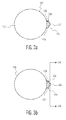
- Figs. 1a and 1b show an exemplary embodiment in accordance with the invention.
- Fig. 1a shows a cross section of cup 110 affixed with disposable metal cover 120 and metal tab 130.
- the diameter of disposable metal cover 120 is typically 10 cm or less.
- disposable metal cover 120 need not be round but may be square, rectangular, octagonal or other suitable geometric shape.
- Metal tab 130 is typically structurally integrated into disposable metal cover 120.
- Fig. 1b shows a top view of cup 110 which is typically hidden below disposable metal cover 120 (see Fig. 1a ).
- the material for disposable metal cover 120 typically includes aluminum.
- disposable metal cover 120 and tab 130 have an RFID tag antenna integrated into them.
- Conducting layer 210 of disposable metal cover 120 and tab 130 is typically made of aluminum, typically thicker than about 5 ⁇ m, and is attached using glue layer 220 to insulating substrate 230.
- insulating substrate 230 is typically made of plastic such as polyethylene terephthalate (PET) but may be made of another suitable insulator and is typically thicker than the skin depth at the operating UHF frequency.
- Glue layer 220 may be formed by the partial melting of insulating substrate 230 during the lamination process used to create disposable metal cover 120 and tab 130 when a plastic such as PET is used.
- the laminating process typically combines a sheet of metal or metal foil (e.g. aluminum) with one or more other materials such as paper or plastic (e.g. PET) using a glue, pressure and typically heat for controlling glue viscosity and drying or thermosetting the bonding agent.
- metal or metal foil e.g. aluminum
- other materials such as paper or plastic (e.g. PET)
- glue, pressure and typically heat for controlling glue viscosity and drying or thermosetting the bonding agent.
- Insulating substrate 230 is attached to the rim of cup 110 using glue layer 240.
- Typical thicknesses for insulating substrate 230 are on the order of from about 20 ⁇ m to about 100 ⁇ m.
- Glue layer 240 is typically a glue that is suitable for attachment to the rim of cup 110.
- UHF RFID matching network 310 may be integrated directly into disposable metal cover 120 and tab 130 by cutting or etching a matching loop formed by arms 128 and 129 into conducting layer 210 on tab 130 and form part of UHF RFID matching network 310.
- a typical three-dimensional electromagnetic simulation software program used for design of UHF RFID matching network 310 is CST MICROWAVE STUDIO available from COMPUTER SIMULATION TECHNOLOGY OF AMERICA, Inc. 429 Old Connecticut Path, Suite 505, Framingham, MA 01701.
- UHF RFID integrated circuit (IC) 330 maybe directly attached to matching network 310 or to UHF RFID STRAP carrier 520 (see Fig. 5 ) which is attached to matching network 310.
- Fig. 3a shows arm 128 and arm 129 of UHF RFID matching network 310 (see Figs. 3b and 3c ) on tab 130.
- part of metal layer 210 on tab 130 is precisely removed to create arm 128 and arm 129 using an appropriate etchant and mask or other suitable process for the metal used for metal layer 210 and exposing an area of insulating substrate 230 on tab 130.
- the size of the area enclosed by arm 128 and arm 129 is typically adjusted to provide the desired UHF RFID matching network 310.
- Note notch 127 in Fig. 3 a that is etched or otherwise introduced into metal layer 210 to provide an attachment location for UHF RFID IC 330.
- UHF RFID matching network 310 functions to match the impedance of disposable metal cover 120 to UHF RFID IC 330 as shown in Fig. 3b . Maximum power is delivered from the RFID reader to disposable metal cover 120 when the input impedance of disposable metal cover 120 is the complex conjugate of the impedance of UHF RFID IC 330 (conjugate impedance matching).
- a typical complex impedance for UHF RFID IC 330 is, for example, (10 ⁇ 150j) ⁇ .
- UHF RFID IC 330 may be directly attached to UHF matching network 310 (see Fig. 4 ) or to UHF RFID STRAP carrier 520 which is attached to UHF matching network 310 (see Fig. 5 ).
- Fig. 3c shows the relationship of an embodiment in accordance with the invention to an equivalent circuit model.
- Equivalent circuit model 360 corresponds to disposable metal cover 120 which functions as a UHF RFID antenna having inductance 362, capacitance 364 and resistance 366.
- typical values for inductance 362 are in the range from about 30 nH to about 50 nH
- typical values for capacitance 364 are in the range from about 0.2 pF to about 2 pF
- typical values for resistance 366 are in the range from about 5 ⁇ to about 100 S2, at the operating frequency that is typically about 915 MHz.
- Equivalent circuit model 370 shows the "T-match” configuration that is created by T-match arms 128 and 129 together with disposable metal cover 120.
- the "T-match” configuration acts as an impedance transformer to match the impedance of disposable metal cover 120 to UHF RFID IC 330.
- the impedance transformer in equivalent circuit model 370 is typically adjusted by controlling the area of insulating substrate 230 enclosed by arms 128 and 129 (e.g. making the arms 128 and 129 wider or narrower as well as longer or shorter). For example, the input impedance may be increased if the width of arms 128 and 129 is decreased.
- the impedance step up ratio provided by inductors 372 and 374 depends on the current division factor between metal cover 120 and arms 128 and 129.
- T-match configurations may be found in "The art of UHF RFID antenna design: impedance matching and size reduction techniques" by Gaetano Marrocco, IEEE Antennas and Propagation Magazine, Vol. 50, No. 1, pp. 66-79, 2008 which is hereby incorporated by reference in its entirety.
- Equivalent circuit model 380 corresponds to inductances 382 and 384 of metal arms 128 and 129, respectively, on tab 130 that connect UHF RFID IC 330 to disposable metal cover 120.
- a typical value for inductances 382 and 384 is on the order of about 10 nH.
- equivalent circuit model 390 corresponds to resistance 392 and capacitance 394 of UHF RFID IC 330.
- a typical value for resistance 392 is on the order of about 2 OF2 and a typical value for capacitance 394 is on the order of about 1 pF.
- FIG. 4 shows UHF RFID IC 330 directly attached to arms 128 and 129 in cross-sectional view 350 (see Fig. 3b ) to provide a connection for UHF RFID IC 330 to matching network 310.
- Matching network 310 is attached to insulating layer 230 by glue layer 220.
- Fig. 5 shows the use of UHF RFID STRAP carrier 520 to connect UHF RFID IC 330 to matching network 310 in cross-sectional view 350 (see Fig. 3b ).
- UHF RFID STRAP carrier 520 is attached to arms 128 and 129 which form a matching loop structure. Note that in accordance with the invention, the shape does not need to be a loop and could be, for example, semi-rectangular. Arms 128 and 129 are attached to insulating layer 230 by glue layer 220.
- UHF RFID IC 330 is typically directly attached to UHF RFID STRAP carrier 520.
- Fig. 6a shows the imaginary value of the complex impedance as a function of frequency at notch 127 for six different distances of the center of notch 127 on tab 130 from the perimeter of disposable metal cover 120 having a diameter on the order of about 50 mm. (e.g see Fig. 3a ). All other values are fixed so that arms 128 and 129 enclose less area as the location of notch 127 is moved inward a total of about 9.5 mm and the imaginary impedance decreases as the inductance is reduced. Notch 127 is successively moved in by about 1.9 mm.
- Curve 610 shows the imaginary impedance as a function of frequency at notch 127 for the reference position where notch 127 is about 15.5 5 mm away from the perimeter of disposable metal cover 120.
- Curve 620 shows the imaginary impedance as a function of frequency at notch 127 where notch 127 is about 1.9 mm closer to the perimeter of disposable metal cover 120 than for curve 610.
- Curve 630 shows the imaginary impedance as a function of frequency at notch 127 where notch 127 is about 1.9 mm closer to the perimeter of disposable metal cover 120 than for curve 620.
- Curve 640 shows the imaginary impedance as a function of frequency at notch 127 where notch 127 is about 1.9 mm closer to the perimeter of disposable metal cover 120 than for curve 630.
- Curve 650 shows the imaginary impedance as a function of frequency at notch 127 where notch 127 is about 1.9 mm closer to the perimeter of disposable metal cover 120 than for curve 640.
- Curve 660 shows the imaginary impedance as a function of frequency at notch 127 where notch 127 is about 1.9 mm closer to the perimeter of disposable metal cover 120 than for curve 650 and notch 127 is a distance of about 6 mm away from the perimeter of disposable metal cover 120 for curve 660.
- Fig. 6b shows the real value of the complex impedance as a function of frequency at notch 127 for six different distances of the center of notch 127 on tab 130 from the perimeter of disposable metal cover 120 having a diameter on the order of about 50 mm (e.g see Fig. 3a ). All other values are fixed so that arms 128 and 129 enclose less area as the location of notch 127 is moved inward a total of about 9.5 mm and the real impedance decreases as the inductance is reduced. Notch 127 is successively moved in by about 1.9 mm.
- Curve 615 shows the real impedance as a function of frequency at notch 127 for the reference position where notch 127 is about 15.5 mm away from the perimeter of disposable metal cover 120.
- Curve 625 shows the real impedance as a function of frequency at notch 127 where notch 127 is about 1.9 mm closer to the perimeter of disposable metal cover 120 than for curve 615.
- Curve 635 shows the real impedance as a function of frequency at notch 127 where notch 127 is about 1.9 mm closer to the perimeter of disposable metal cover 120 than for curve 625.
- Curve 645 shows the real impedance as a function of frequency at notch 127 where notch 127 is about 1.9 mm closer to the perimeter of disposable metal cover 120 than for curve 635.
- Curve 655 shows the real impedance as a function of frequency at notch 127 where notch 127 is about 1.9 mm closer to the perimeter of disposable metal cover 120 than for curve 645.
- Curve 665 shows the real impedance as a function of frequency at notch 127 where notch 127 is about 1.9 mm closer to the perimeter of disposable metal cover 120 than for curve 655 and notch 127 is a distance of about 6 mm away from the perimeter of disposable metal cover 120 for curve 665.
- impedance matching techniques such as nested shape slot techniques which typically require a different location for the attachment of the UHF RFID IC to the disposable metal cover.
Landscapes
- Engineering & Computer Science (AREA)
- Microelectronics & Electronic Packaging (AREA)
- Computer Hardware Design (AREA)
- Physics & Mathematics (AREA)
- General Physics & Mathematics (AREA)
- Theoretical Computer Science (AREA)
- Computer Networks & Wireless Communication (AREA)
- Details Of Aerials (AREA)
Abstract
Description
- Radio Frequency Identification (RFID) tag and reader systems operate over a wide range of radio frequencies, including low frequency (LF) applications, high frequency (HF) applications and ultra-high frequency applications (UHF). LF applications typically reside in the range from about 125 to about 148.5 kHz, HF applications typically operate at about 13.56 MHz while UHF applications typically reside in the range from about 300 MHz to about 3 GHz. The "read range" of an RFID tag is typically defined as the distance from which the RFID reader can communicate with the RFID tag. Passive LF and HF applications typically provide only very short read ranges and typically require the RFID reader to be separated from the tag by no more than about 2 centimeters to about 30 centimeters to achieve successful communication. Passive UHF applications typically allow for longer read ranges, enabling RFID tags to be located from about 2 meters to about 12 meters or more for successful communication with an RFID reader. Typically, various environmental factors can detune an RFID tag and modify the operating frequency to potentially affect the power received by the RFID tag. This affects the read range for the RFID tag. For example, RFID tags in the presence of conducting media such as metals and liquids may experience detuning due to absorption or parasitic capacitance. Detuning may also arise from the capacitance spread in the assembly process. For example, if the direct attaching process of the RFID tag to the antenna has a misalignment or an imperfect contact, parasitic capacitance may be introduced.
-
-
Fig. 1a shows an embodiment in accordance with the invention. -
Fig. 1b shows a top view ofFig. 1a -
Fig. 2 shows an embodiment in accordance with the invention. -
Fig. 3a shows an embodiment in accordance with the invention. -
Fig. 3b shows an embodiment in accordance with the invention. -
Fig. 3c shows an embodiment in accordance with the invention. -
Fig. 4 shows an embodiment in accordance with the invention. -
Fig. 5 shows an embodiment in accordance with the invention. -
Fig. 6a shows a graph of values of the imaginary impedance of the matching network for embodiments in accordance with the invention. -
Fig. 6b shows a graph of values of the real impedance of the matching network for embodiments in accordance with the invention. - In accordance with the invention, containers having a disposable metal cover, such as, for example, plastic, foam, metal or cardboard cups with a metal foil cover can be RFID tagged by integrating the UHF RFID antenna into the packaging, in particular, disposable metal cover 120 (see
Figs 1a and 1b ). Typical consumer examples of these container types are yogurt cups or dehydrated soup cups. Ifcup 110 is metal, there may exist resonances betweencup 110 anddisposable metal cover 120 which effect the resonance frequency ofdisposable metal cover 120 which operates as a UHF antenna. Havingcup 110 made of metal introduces an extra capacitance fromdisposable metal cover 120 to ground and introduces inductive coupling betweencup 110 and UHF RFID matching network 310 (e.g. seeFigs. 3b and3c ). Additionally, ifcup 110 is metal, the volume ofcup 110 will typically effect the design. Note that the effects of havingcup 110 made of metal can typically be mitigated by appropriate design of UHF RFID matching network 310 (e.g. seeFig. 3b ) and because the resonance ofdisposable metal cover 120 which functions as the UHF antenna is typically more than about 50 to about 100 MHz higher than the operating frequency in accordance with the invention. The UHF RFID antenna integrated intodisposable metal cover 120 receives power from the RFID reader and that power is used to activate UHF RFID Integrated Circuit (IC) 330 (seeFig. 3b ). Typical power output for the RFID reader is on the order of 4 watts and UHF RFID IC 330 (seeFig. 3b ) typically needs a power level of -18 dBm for activation in reading mode and typically needs a power level of -15 dBm for activation in write mode. Embodiments in accordance with the invention have typical Q (quality factor) values less than about 20 and the embodiments in accordance with the invention function in both the radiative near field zone and in the radiation zone. -
Figs. 1a and 1b show an exemplary embodiment in accordance with the invention.Fig. 1a shows a cross section ofcup 110 affixed withdisposable metal cover 120 andmetal tab 130. In accordance with an embodiment of the invention, the diameter ofdisposable metal cover 120 is typically 10 cm or less. Note that in accordance with the invention,disposable metal cover 120 need not be round but may be square, rectangular, octagonal or other suitable geometric shape.Metal tab 130 is typically structurally integrated intodisposable metal cover 120.Fig. 1b shows a top view ofcup 110 which is typically hidden below disposable metal cover 120 (seeFig. 1a ). The material fordisposable metal cover 120 typically includes aluminum. In accordance with the invention,disposable metal cover 120 andtab 130 have an RFID tag antenna integrated into them.Fig. 2 shows a cross-section ofmultilayer structure 200 that is used fordisposable metal cover 120 andtab 130. Conductinglayer 210 ofdisposable metal cover 120 andtab 130 is typically made of aluminum, typically thicker than about 5 µm, and is attached usingglue layer 220 to insulatingsubstrate 230. In accordance with the invention,insulating substrate 230 is typically made of plastic such as polyethylene terephthalate (PET) but may be made of another suitable insulator and is typically thicker than the skin depth at the operating UHF frequency.Glue layer 220 may be formed by the partial melting ofinsulating substrate 230 during the lamination process used to createdisposable metal cover 120 andtab 130 when a plastic such as PET is used. In accordance with the invention, the laminating process typically combines a sheet of metal or metal foil (e.g. aluminum) with one or more other materials such as paper or plastic (e.g. PET) using a glue, pressure and typically heat for controlling glue viscosity and drying or thermosetting the bonding agent. Four typical methods for laminating aluminum foil are wet bonding, dry pressure or thermoplastic-bonding, extrusion bonding and hot melt bonding. -
Insulating substrate 230 is attached to the rim ofcup 110 usingglue layer 240. Typical thicknesses forinsulating substrate 230 are on the order of from about 20 µm to about 100 µm.Glue layer 240 is typically a glue that is suitable for attachment to the rim ofcup 110. - Due to the mechanical design of
disposable metal cover 130 havinginsulating substrate 230 coated with conductinglayer 210, UHF RFID matching network 310 (seeFig. 3b ) may be integrated directly intodisposable metal cover 120 andtab 130 by cutting or etching a matching loop formed byarms layer 210 ontab 130 and form part of UHFRFID matching network 310. A typical three-dimensional electromagnetic simulation software program used for design of UHFRFID matching network 310 is CST MICROWAVE STUDIO available from COMPUTER SIMULATION TECHNOLOGY OF AMERICA, Inc. 429 Old Connecticut Path, Suite 505, Framingham, MA 01701. UHF RFID integrated circuit (IC) 330 (seeFig. 3a ) maybe directly attached to matchingnetwork 310 or to UHF RFID STRAP carrier 520 (seeFig. 5 ) which is attached to matchingnetwork 310. -
Fig. 3a showsarm 128 andarm 129 of UHF RFID matching network 310 (seeFigs. 3b and3c ) ontab 130. In accordance with an embodiment of the invention, part ofmetal layer 210 ontab 130 is precisely removed to createarm 128 andarm 129 using an appropriate etchant and mask or other suitable process for the metal used formetal layer 210 and exposing an area of insulatingsubstrate 230 ontab 130. The size of the area enclosed byarm 128 andarm 129 is typically adjusted to provide the desired UHFRFID matching network 310. Notenotch 127 inFig. 3 a that is etched or otherwise introduced intometal layer 210 to provide an attachment location forUHF RFID IC 330. - UHF
RFID matching network 310 functions to match the impedance ofdisposable metal cover 120 toUHF RFID IC 330 as shown inFig. 3b . Maximum power is delivered from the RFID reader todisposable metal cover 120 when the input impedance ofdisposable metal cover 120 is the complex conjugate of the impedance of UHF RFID IC 330 (conjugate impedance matching). A typical complex impedance forUHF RFID IC 330 is, for example, (10 ― 150j) Ω.UHF RFID IC 330 may be directly attached to UHF matching network 310 (seeFig. 4 ) or to UHFRFID STRAP carrier 520 which is attached to UHF matching network 310 (seeFig. 5 ). -
Fig. 3c shows the relationship of an embodiment in accordance with the invention to an equivalent circuit model.Equivalent circuit model 360 corresponds todisposable metal cover 120 which functions as a UHF RFIDantenna having inductance 362,capacitance 364 andresistance 366. In accordance with the invention, typical values forinductance 362 are in the range from about 30 nH to about 50 nH, typical values forcapacitance 364 are in the range from about 0.2 pF to about 2 pF and typical values forresistance 366 are in the range from about 5 Ω to about 100 S2, at the operating frequency that is typically about 915 MHz. -
Equivalent circuit model 370 shows the "T-match" configuration that is created by T-match arms disposable metal cover 120. The "T-match" configuration acts as an impedance transformer to match the impedance ofdisposable metal cover 120 toUHF RFID IC 330. The impedance transformer inequivalent circuit model 370 is typically adjusted by controlling the area of insulatingsubstrate 230 enclosed byarms 128 and 129 (e.g. making thearms arms inductors metal cover 120 andarms -
Equivalent circuit model 380 corresponds to inductances 382 and 384 ofmetal arms tab 130 that connectUHF RFID IC 330 todisposable metal cover 120. A typical value forinductances equivalent circuit model 390 corresponds toresistance 392 andcapacitance 394 ofUHF RFID IC 330. A typical value forresistance 392 is on the order of about 2 OF2 and a typical value forcapacitance 394 is on the order of about 1 pF. - In accordance with an embodiment of the invention,
FIG. 4 showsUHF RFID IC 330 directly attached toarms Fig. 3b ) to provide a connection forUHF RFID IC 330 to matchingnetwork 310.Matching network 310 is attached to insulatinglayer 230 byglue layer 220. - In accordance with an embodiment of the invention,
Fig. 5 shows the use of UHFRFID STRAP carrier 520 to connectUHF RFID IC 330 to matchingnetwork 310 in cross-sectional view 350 (seeFig. 3b ). UHFRFID STRAP carrier 520 is attached toarms Arms layer 230 byglue layer 220.UHF RFID IC 330 is typically directly attached to UHFRFID STRAP carrier 520. - In accordance with the invention,
Fig. 6a shows the imaginary value of the complex impedance as a function of frequency atnotch 127 for six different distances of the center ofnotch 127 ontab 130 from the perimeter ofdisposable metal cover 120 having a diameter on the order of about 50 mm. (e.g seeFig. 3a ). All other values are fixed so thatarms notch 127 is moved inward a total of about 9.5 mm and the imaginary impedance decreases as the inductance is reduced.Notch 127 is successively moved in by about 1.9 mm.Curve 610 shows the imaginary impedance as a function of frequency atnotch 127 for the reference position wherenotch 127 is about 15.5 5 mm away from the perimeter ofdisposable metal cover 120.Curve 620 shows the imaginary impedance as a function of frequency atnotch 127 wherenotch 127 is about 1.9 mm closer to the perimeter ofdisposable metal cover 120 than forcurve 610.Curve 630 shows the imaginary impedance as a function of frequency atnotch 127 wherenotch 127 is about 1.9 mm closer to the perimeter ofdisposable metal cover 120 than forcurve 620.Curve 640 shows the imaginary impedance as a function of frequency atnotch 127 wherenotch 127 is about 1.9 mm closer to the perimeter ofdisposable metal cover 120 than forcurve 630.Curve 650 shows the imaginary impedance as a function of frequency atnotch 127 wherenotch 127 is about 1.9 mm closer to the perimeter ofdisposable metal cover 120 than forcurve 640.Curve 660 shows the imaginary impedance as a function of frequency atnotch 127 wherenotch 127 is about 1.9 mm closer to the perimeter ofdisposable metal cover 120 than forcurve 650 and notch 127 is a distance of about 6 mm away from the perimeter ofdisposable metal cover 120 forcurve 660. - In accordance with the invention,
Fig. 6b shows the real value of the complex impedance as a function of frequency atnotch 127 for six different distances of the center ofnotch 127 ontab 130 from the perimeter ofdisposable metal cover 120 having a diameter on the order of about 50 mm (e.g seeFig. 3a ). All other values are fixed so thatarms notch 127 is moved inward a total of about 9.5 mm and the real impedance decreases as the inductance is reduced.Notch 127 is successively moved in by about 1.9 mm.Curve 615 shows the real impedance as a function of frequency atnotch 127 for the reference position wherenotch 127 is about 15.5 mm away from the perimeter ofdisposable metal cover 120.Curve 625 shows the real impedance as a function of frequency atnotch 127 wherenotch 127 is about 1.9 mm closer to the perimeter ofdisposable metal cover 120 than forcurve 615.Curve 635 shows the real impedance as a function of frequency atnotch 127 wherenotch 127 is about 1.9 mm closer to the perimeter ofdisposable metal cover 120 than forcurve 625.Curve 645 shows the real impedance as a function of frequency atnotch 127 wherenotch 127 is about 1.9 mm closer to the perimeter ofdisposable metal cover 120 than forcurve 635.Curve 655 shows the real impedance as a function of frequency atnotch 127 wherenotch 127 is about 1.9 mm closer to the perimeter ofdisposable metal cover 120 than forcurve 645.Curve 665 shows the real impedance as a function of frequency atnotch 127 wherenotch 127 is about 1.9 mm closer to the perimeter ofdisposable metal cover 120 than forcurve 655 and notch 127 is a distance of about 6 mm away from the perimeter ofdisposable metal cover 120 forcurve 665. - As will be apparent to those skilled in the art, in accordance with the invention other impedance matching techniques may be used, such as nested shape slot techniques which typically require a different location for the attachment of the UHF RFID IC to the disposable metal cover.
- While the invention has been described in conjunction with specific embodiments, it is evident to those skilled in the art that many alternatives, modifications, and variations will be apparent in light of the foregoing description. Accordingly, the invention is intended to embrace all other such alternatives, modifications, and variations that fall within the spirit and scope of the appended claims.
Claims (9)
- A UHF RFID antenna system comprising:a disposable metal cover comprising a metal layer and an insulating layer; anda tab integrally formed with said disposable metal cover such that said tab shares a portion of said metal layer and a portion of said insulating layer with said disposable metal cover, said tab having part of said portion of said metal layer removed to form a matching loop electrically coupled to said disposable metal cover.
- The UHF RFID antenna system of Claim 1 further comprising a container affixed to said disposable metal cover.
- The UHF RFID antenna system of Claim 1 wherein said insulating layer is comprised of PET.
- The UHF RFID antenna system of Claim 1 wherein said metal cover is comprised of aluminum.
- The UHF RFID antenna system of Claim 1 wherein said matching loop is comprised of a first arm and a second arm, sad first arm and said second arm being electrically coupled and directly attached to a UHF RFID IC.
- The UHF RFID antenna system of Claim 1 wherein said matching loop is comprised of a first arm and a second arm, said first arm and said second arm being electrically coupled to and directly attached to a UHF RFID STRAP carrier.
- The UHF RFID antenna system of Claim 1 wherein said UHF RFID STRAP carrier is electrically coupled to a UHF RFID IC.
- The UHF RFID antenna system of Claim 2 wherein said container is comprised of a material selected from the group containing foam, plastic, metal and cardboard.
- The UHF RFID antenna system of Claim 1 wherein said disposable metal cover has a generally circular shape.
Applications Claiming Priority (1)
| Application Number | Priority Date | Filing Date | Title |
|---|---|---|---|
| US12/841,093 US8339318B2 (en) | 2010-07-21 | 2010-07-21 | RFID UHF antenna and matching network embedded in disposable conducting covers |
Publications (2)
| Publication Number | Publication Date |
|---|---|
| EP2410604A1 true EP2410604A1 (en) | 2012-01-25 |
| EP2410604B1 EP2410604B1 (en) | 2015-10-14 |
Family
ID=44789305
Family Applications (1)
| Application Number | Title | Priority Date | Filing Date |
|---|---|---|---|
| EP11174939.6A Not-in-force EP2410604B1 (en) | 2010-07-21 | 2011-07-21 | RFID UHF antenna and matching network embedded in disposable metal cover |
Country Status (3)
| Country | Link |
|---|---|
| US (1) | US8339318B2 (en) |
| EP (1) | EP2410604B1 (en) |
| CN (1) | CN102347528B (en) |
Cited By (1)
| Publication number | Priority date | Publication date | Assignee | Title |
|---|---|---|---|---|
| WO2014029628A1 (en) * | 2012-08-22 | 2014-02-27 | Nestec S.A. | Capsule assemblies with data storage and communication means |
Families Citing this family (3)
| Publication number | Priority date | Publication date | Assignee | Title |
|---|---|---|---|---|
| EP2645298A1 (en) | 2012-03-30 | 2013-10-02 | austriamicrosystems AG | Portable object and information transmission system |
| US9390367B2 (en) | 2014-07-08 | 2016-07-12 | Wernher von Braun Centro de Pesquisas Avancadas | RFID tag and RFID tag antenna |
| US20250148255A1 (en) * | 2022-02-09 | 2025-05-08 | Avery Dennison Retail Information Services Llc | Metallic packaging containing an integrated rfid inlay |
Citations (3)
| Publication number | Priority date | Publication date | Assignee | Title |
|---|---|---|---|---|
| US6215402B1 (en) * | 1998-03-13 | 2001-04-10 | Intermec Ip Corp. | Radio frequency identification transponder employing patch antenna |
| EP1988491A1 (en) * | 2006-02-22 | 2008-11-05 | Toyo Seikan Kaisya, Ltd. | Base material for rfid tag adapted to metallic material |
| WO2009142146A1 (en) * | 2008-05-20 | 2009-11-26 | 東洋製罐株式会社 | Metallic cover having ic tag, and metallic container |
Family Cites Families (8)
| Publication number | Priority date | Publication date | Assignee | Title |
|---|---|---|---|---|
| US5826328A (en) * | 1996-03-25 | 1998-10-27 | International Business Machines | Method of making a thin radio frequency transponder |
| US6107920A (en) | 1998-06-09 | 2000-08-22 | Motorola, Inc. | Radio frequency identification tag having an article integrated antenna |
| US20050263524A1 (en) * | 2004-05-28 | 2005-12-01 | Ipl, Inc. | Container lid with removable seal layer |
| KR100615387B1 (en) | 2004-08-25 | 2006-08-31 | 최정곤 | Container lid with wireless tag |
| US7887755B2 (en) * | 2006-09-20 | 2011-02-15 | Binforma Group Limited Liability Company | Packaging closures integrated with disposable RFID devices |
| US20090045959A1 (en) * | 2007-08-16 | 2009-02-19 | Lottabase, Llc. | Beverage container authenticity and provenance devices and methods |
| US7705734B2 (en) * | 2006-12-21 | 2010-04-27 | Martinelli Lawrence G | Secure product packaging |
| KR100899901B1 (en) | 2008-10-27 | 2009-05-29 | 대한민국 | Container lid with wireless tag |
-
2010
- 2010-07-21 US US12/841,093 patent/US8339318B2/en active Active
-
2011
- 2011-07-20 CN CN201110203648.5A patent/CN102347528B/en not_active Expired - Fee Related
- 2011-07-21 EP EP11174939.6A patent/EP2410604B1/en not_active Not-in-force
Patent Citations (3)
| Publication number | Priority date | Publication date | Assignee | Title |
|---|---|---|---|---|
| US6215402B1 (en) * | 1998-03-13 | 2001-04-10 | Intermec Ip Corp. | Radio frequency identification transponder employing patch antenna |
| EP1988491A1 (en) * | 2006-02-22 | 2008-11-05 | Toyo Seikan Kaisya, Ltd. | Base material for rfid tag adapted to metallic material |
| WO2009142146A1 (en) * | 2008-05-20 | 2009-11-26 | 東洋製罐株式会社 | Metallic cover having ic tag, and metallic container |
Non-Patent Citations (1)
| Title |
|---|
| GAETANO MARROCCO: "The art of UHF RFID antenna design: impedance matching and size reduction techniques", IEEE ANTENNAS AND PROPAGATION MAGAZINE, vol. 50, no. 1, 2008, pages 66 - 79 |
Cited By (1)
| Publication number | Priority date | Publication date | Assignee | Title |
|---|---|---|---|---|
| WO2014029628A1 (en) * | 2012-08-22 | 2014-02-27 | Nestec S.A. | Capsule assemblies with data storage and communication means |
Also Published As
| Publication number | Publication date |
|---|---|
| EP2410604B1 (en) | 2015-10-14 |
| US8339318B2 (en) | 2012-12-25 |
| US20120019417A1 (en) | 2012-01-26 |
| CN102347528A (en) | 2012-02-08 |
| CN102347528B (en) | 2014-05-28 |
Similar Documents
| Publication | Publication Date | Title |
|---|---|---|
| US9172130B2 (en) | RFID inlay incorporating a ground plane | |
| US7202790B2 (en) | Techniques for tuning an antenna to different operating frequencies | |
| US8289165B2 (en) | RFID device with conductive loop shield | |
| EP1817756B1 (en) | Combination eas and rfid label or tag | |
| US8477076B1 (en) | Antenna coupler mechanism | |
| US9390603B2 (en) | Dual EAS-RFID security tag | |
| US9010648B2 (en) | Antenna and RFID tag | |
| TWI434217B (en) | Wireless tag | |
| KR101724611B1 (en) | RFID tag antenna | |
| CN112352247B (en) | Method of using a shielding RFID tape with an RFID tag design | |
| EP2220596A1 (en) | Combination eas and rfid label or tag using a hybrid rfid antenna | |
| EP2220628A1 (en) | Combination eas and rfid label or tag with controllable read range using a hybrid rfid antenna | |
| US10192160B2 (en) | Radio-frequency identification device | |
| JP2014533057A (en) | Antenna structure and RFID transponder system provided with antenna structure | |
| US8477077B1 (en) | Antenna coupler mechanism systems and methods | |
| JP4927665B2 (en) | Auxiliary antenna for RFID tag and its mounting method | |
| EP2410604B1 (en) | RFID UHF antenna and matching network embedded in disposable metal cover | |
| US10084227B2 (en) | Antenna coupler mechanism | |
| US20250165742A1 (en) | On-metal uhf rfid tag |
Legal Events
| Date | Code | Title | Description |
|---|---|---|---|
| AK | Designated contracting states |
Kind code of ref document: A1 Designated state(s): AL AT BE BG CH CY CZ DE DK EE ES FI FR GB GR HR HU IE IS IT LI LT LU LV MC MK MT NL NO PL PT RO RS SE SI SK SM TR |
|
| AX | Request for extension of the european patent |
Extension state: BA ME |
|
| PUAI | Public reference made under article 153(3) epc to a published international application that has entered the european phase |
Free format text: ORIGINAL CODE: 0009012 |
|
| 17P | Request for examination filed |
Effective date: 20120725 |
|
| GRAP | Despatch of communication of intention to grant a patent |
Free format text: ORIGINAL CODE: EPIDOSNIGR1 |
|
| INTG | Intention to grant announced |
Effective date: 20150521 |
|
| GRAS | Grant fee paid |
Free format text: ORIGINAL CODE: EPIDOSNIGR3 |
|
| GRAA | (expected) grant |
Free format text: ORIGINAL CODE: 0009210 |
|
| AK | Designated contracting states |
Kind code of ref document: B1 Designated state(s): AL AT BE BG CH CY CZ DE DK EE ES FI FR GB GR HR HU IE IS IT LI LT LU LV MC MK MT NL NO PL PT RO RS SE SI SK SM TR |
|
| REG | Reference to a national code |
Ref country code: GB Ref legal event code: FG4D |
|
| REG | Reference to a national code |
Ref country code: AT Ref legal event code: REF Ref document number: 755717 Country of ref document: AT Kind code of ref document: T Effective date: 20151015 Ref country code: CH Ref legal event code: EP |
|
| REG | Reference to a national code |
Ref country code: IE Ref legal event code: FG4D |
|
| REG | Reference to a national code |
Ref country code: DE Ref legal event code: R096 Ref document number: 602011020521 Country of ref document: DE |
|
| REG | Reference to a national code |
Ref country code: NL Ref legal event code: MP Effective date: 20151014 |
|
| REG | Reference to a national code |
Ref country code: LT Ref legal event code: MG4D |
|
| REG | Reference to a national code |
Ref country code: AT Ref legal event code: MK05 Ref document number: 755717 Country of ref document: AT Kind code of ref document: T Effective date: 20151014 |
|
| PG25 | Lapsed in a contracting state [announced via postgrant information from national office to epo] |
Ref country code: IS Free format text: LAPSE BECAUSE OF FAILURE TO SUBMIT A TRANSLATION OF THE DESCRIPTION OR TO PAY THE FEE WITHIN THE PRESCRIBED TIME-LIMIT Effective date: 20160214 Ref country code: HR Free format text: LAPSE BECAUSE OF FAILURE TO SUBMIT A TRANSLATION OF THE DESCRIPTION OR TO PAY THE FEE WITHIN THE PRESCRIBED TIME-LIMIT Effective date: 20151014 Ref country code: LT Free format text: LAPSE BECAUSE OF FAILURE TO SUBMIT A TRANSLATION OF THE DESCRIPTION OR TO PAY THE FEE WITHIN THE PRESCRIBED TIME-LIMIT Effective date: 20151014 Ref country code: IT Free format text: LAPSE BECAUSE OF FAILURE TO SUBMIT A TRANSLATION OF THE DESCRIPTION OR TO PAY THE FEE WITHIN THE PRESCRIBED TIME-LIMIT Effective date: 20151014 Ref country code: NL Free format text: LAPSE BECAUSE OF FAILURE TO SUBMIT A TRANSLATION OF THE DESCRIPTION OR TO PAY THE FEE WITHIN THE PRESCRIBED TIME-LIMIT Effective date: 20151014 Ref country code: ES Free format text: LAPSE BECAUSE OF FAILURE TO SUBMIT A TRANSLATION OF THE DESCRIPTION OR TO PAY THE FEE WITHIN THE PRESCRIBED TIME-LIMIT Effective date: 20151014 Ref country code: NO Free format text: LAPSE BECAUSE OF FAILURE TO SUBMIT A TRANSLATION OF THE DESCRIPTION OR TO PAY THE FEE WITHIN THE PRESCRIBED TIME-LIMIT Effective date: 20160114 |
|
| PG25 | Lapsed in a contracting state [announced via postgrant information from national office to epo] |
Ref country code: PT Free format text: LAPSE BECAUSE OF FAILURE TO SUBMIT A TRANSLATION OF THE DESCRIPTION OR TO PAY THE FEE WITHIN THE PRESCRIBED TIME-LIMIT Effective date: 20160215 Ref country code: GR Free format text: LAPSE BECAUSE OF FAILURE TO SUBMIT A TRANSLATION OF THE DESCRIPTION OR TO PAY THE FEE WITHIN THE PRESCRIBED TIME-LIMIT Effective date: 20160115 Ref country code: RS Free format text: LAPSE BECAUSE OF FAILURE TO SUBMIT A TRANSLATION OF THE DESCRIPTION OR TO PAY THE FEE WITHIN THE PRESCRIBED TIME-LIMIT Effective date: 20151014 Ref country code: AT Free format text: LAPSE BECAUSE OF FAILURE TO SUBMIT A TRANSLATION OF THE DESCRIPTION OR TO PAY THE FEE WITHIN THE PRESCRIBED TIME-LIMIT Effective date: 20151014 Ref country code: LV Free format text: LAPSE BECAUSE OF FAILURE TO SUBMIT A TRANSLATION OF THE DESCRIPTION OR TO PAY THE FEE WITHIN THE PRESCRIBED TIME-LIMIT Effective date: 20151014 Ref country code: SE Free format text: LAPSE BECAUSE OF FAILURE TO SUBMIT A TRANSLATION OF THE DESCRIPTION OR TO PAY THE FEE WITHIN THE PRESCRIBED TIME-LIMIT Effective date: 20151014 Ref country code: PL Free format text: LAPSE BECAUSE OF FAILURE TO SUBMIT A TRANSLATION OF THE DESCRIPTION OR TO PAY THE FEE WITHIN THE PRESCRIBED TIME-LIMIT Effective date: 20151014 Ref country code: FI Free format text: LAPSE BECAUSE OF FAILURE TO SUBMIT A TRANSLATION OF THE DESCRIPTION OR TO PAY THE FEE WITHIN THE PRESCRIBED TIME-LIMIT Effective date: 20151014 |
|
| REG | Reference to a national code |
Ref country code: FR Ref legal event code: PLFP Year of fee payment: 6 |
|
| REG | Reference to a national code |
Ref country code: DE Ref legal event code: R097 Ref document number: 602011020521 Country of ref document: DE |
|
| PG25 | Lapsed in a contracting state [announced via postgrant information from national office to epo] |
Ref country code: CZ Free format text: LAPSE BECAUSE OF FAILURE TO SUBMIT A TRANSLATION OF THE DESCRIPTION OR TO PAY THE FEE WITHIN THE PRESCRIBED TIME-LIMIT Effective date: 20151014 |
|
| PLBE | No opposition filed within time limit |
Free format text: ORIGINAL CODE: 0009261 |
|
| STAA | Information on the status of an ep patent application or granted ep patent |
Free format text: STATUS: NO OPPOSITION FILED WITHIN TIME LIMIT |
|
| PG25 | Lapsed in a contracting state [announced via postgrant information from national office to epo] |
Ref country code: SM Free format text: LAPSE BECAUSE OF FAILURE TO SUBMIT A TRANSLATION OF THE DESCRIPTION OR TO PAY THE FEE WITHIN THE PRESCRIBED TIME-LIMIT Effective date: 20151014 Ref country code: DK Free format text: LAPSE BECAUSE OF FAILURE TO SUBMIT A TRANSLATION OF THE DESCRIPTION OR TO PAY THE FEE WITHIN THE PRESCRIBED TIME-LIMIT Effective date: 20151014 Ref country code: RO Free format text: LAPSE BECAUSE OF FAILURE TO SUBMIT A TRANSLATION OF THE DESCRIPTION OR TO PAY THE FEE WITHIN THE PRESCRIBED TIME-LIMIT Effective date: 20151014 Ref country code: SK Free format text: LAPSE BECAUSE OF FAILURE TO SUBMIT A TRANSLATION OF THE DESCRIPTION OR TO PAY THE FEE WITHIN THE PRESCRIBED TIME-LIMIT Effective date: 20151014 Ref country code: EE Free format text: LAPSE BECAUSE OF FAILURE TO SUBMIT A TRANSLATION OF THE DESCRIPTION OR TO PAY THE FEE WITHIN THE PRESCRIBED TIME-LIMIT Effective date: 20151014 |
|
| 26N | No opposition filed |
Effective date: 20160715 |
|
| PG25 | Lapsed in a contracting state [announced via postgrant information from national office to epo] |
Ref country code: SI Free format text: LAPSE BECAUSE OF FAILURE TO SUBMIT A TRANSLATION OF THE DESCRIPTION OR TO PAY THE FEE WITHIN THE PRESCRIBED TIME-LIMIT Effective date: 20151014 |
|
| PG25 | Lapsed in a contracting state [announced via postgrant information from national office to epo] |
Ref country code: BE Free format text: LAPSE BECAUSE OF FAILURE TO SUBMIT A TRANSLATION OF THE DESCRIPTION OR TO PAY THE FEE WITHIN THE PRESCRIBED TIME-LIMIT Effective date: 20151014 |
|
| REG | Reference to a national code |
Ref country code: CH Ref legal event code: PL |
|
| PG25 | Lapsed in a contracting state [announced via postgrant information from national office to epo] |
Ref country code: MC Free format text: LAPSE BECAUSE OF FAILURE TO SUBMIT A TRANSLATION OF THE DESCRIPTION OR TO PAY THE FEE WITHIN THE PRESCRIBED TIME-LIMIT Effective date: 20151014 |
|
| PG25 | Lapsed in a contracting state [announced via postgrant information from national office to epo] |
Ref country code: CH Free format text: LAPSE BECAUSE OF NON-PAYMENT OF DUE FEES Effective date: 20160731 Ref country code: LI Free format text: LAPSE BECAUSE OF NON-PAYMENT OF DUE FEES Effective date: 20160731 |
|
| REG | Reference to a national code |
Ref country code: IE Ref legal event code: MM4A |
|
| REG | Reference to a national code |
Ref country code: FR Ref legal event code: PLFP Year of fee payment: 7 |
|
| PG25 | Lapsed in a contracting state [announced via postgrant information from national office to epo] |
Ref country code: IE Free format text: LAPSE BECAUSE OF NON-PAYMENT OF DUE FEES Effective date: 20160721 |
|
| PG25 | Lapsed in a contracting state [announced via postgrant information from national office to epo] |
Ref country code: LU Free format text: LAPSE BECAUSE OF NON-PAYMENT OF DUE FEES Effective date: 20160721 |
|
| PG25 | Lapsed in a contracting state [announced via postgrant information from national office to epo] |
Ref country code: HU Free format text: LAPSE BECAUSE OF FAILURE TO SUBMIT A TRANSLATION OF THE DESCRIPTION OR TO PAY THE FEE WITHIN THE PRESCRIBED TIME-LIMIT; INVALID AB INITIO Effective date: 20110721 Ref country code: CY Free format text: LAPSE BECAUSE OF FAILURE TO SUBMIT A TRANSLATION OF THE DESCRIPTION OR TO PAY THE FEE WITHIN THE PRESCRIBED TIME-LIMIT Effective date: 20151014 |
|
| REG | Reference to a national code |
Ref country code: FR Ref legal event code: PLFP Year of fee payment: 8 |
|
| PG25 | Lapsed in a contracting state [announced via postgrant information from national office to epo] |
Ref country code: MT Free format text: LAPSE BECAUSE OF NON-PAYMENT OF DUE FEES Effective date: 20160731 Ref country code: MK Free format text: LAPSE BECAUSE OF FAILURE TO SUBMIT A TRANSLATION OF THE DESCRIPTION OR TO PAY THE FEE WITHIN THE PRESCRIBED TIME-LIMIT Effective date: 20151014 Ref country code: TR Free format text: LAPSE BECAUSE OF FAILURE TO SUBMIT A TRANSLATION OF THE DESCRIPTION OR TO PAY THE FEE WITHIN THE PRESCRIBED TIME-LIMIT Effective date: 20151014 |
|
| PG25 | Lapsed in a contracting state [announced via postgrant information from national office to epo] |
Ref country code: BG Free format text: LAPSE BECAUSE OF FAILURE TO SUBMIT A TRANSLATION OF THE DESCRIPTION OR TO PAY THE FEE WITHIN THE PRESCRIBED TIME-LIMIT Effective date: 20151014 |
|
| PG25 | Lapsed in a contracting state [announced via postgrant information from national office to epo] |
Ref country code: AL Free format text: LAPSE BECAUSE OF FAILURE TO SUBMIT A TRANSLATION OF THE DESCRIPTION OR TO PAY THE FEE WITHIN THE PRESCRIBED TIME-LIMIT Effective date: 20151014 |
|
| PGFP | Annual fee paid to national office [announced via postgrant information from national office to epo] |
Ref country code: FR Payment date: 20190621 Year of fee payment: 9 |
|
| PGFP | Annual fee paid to national office [announced via postgrant information from national office to epo] |
Ref country code: GB Payment date: 20190624 Year of fee payment: 9 Ref country code: DE Payment date: 20190620 Year of fee payment: 9 |
|
| REG | Reference to a national code |
Ref country code: DE Ref legal event code: R119 Ref document number: 602011020521 Country of ref document: DE |
|
| GBPC | Gb: european patent ceased through non-payment of renewal fee |
Effective date: 20200721 |
|
| PG25 | Lapsed in a contracting state [announced via postgrant information from national office to epo] |
Ref country code: FR Free format text: LAPSE BECAUSE OF NON-PAYMENT OF DUE FEES Effective date: 20200731 Ref country code: GB Free format text: LAPSE BECAUSE OF NON-PAYMENT OF DUE FEES Effective date: 20200721 |
|
| PG25 | Lapsed in a contracting state [announced via postgrant information from national office to epo] |
Ref country code: DE Free format text: LAPSE BECAUSE OF NON-PAYMENT OF DUE FEES Effective date: 20210202 |