EP2408094A2 - Discharge loop for power supply circuit and active control circuit thereof - Google Patents
Discharge loop for power supply circuit and active control circuit thereof Download PDFInfo
- Publication number
- EP2408094A2 EP2408094A2 EP11001093A EP11001093A EP2408094A2 EP 2408094 A2 EP2408094 A2 EP 2408094A2 EP 11001093 A EP11001093 A EP 11001093A EP 11001093 A EP11001093 A EP 11001093A EP 2408094 A2 EP2408094 A2 EP 2408094A2
- Authority
- EP
- European Patent Office
- Prior art keywords
- voltage
- power supply
- switch
- input
- supply circuit
- Prior art date
- Legal status (The legal status is an assumption and is not a legal conclusion. Google has not performed a legal analysis and makes no representation as to the accuracy of the status listed.)
- Withdrawn
Links
- 238000007599 discharging Methods 0.000 claims abstract description 11
- 239000003990 capacitor Substances 0.000 claims description 72
- 238000001914 filtration Methods 0.000 claims description 62
- 238000012544 monitoring process Methods 0.000 claims description 5
- 230000005669 field effect Effects 0.000 claims description 4
- 239000004065 semiconductor Substances 0.000 claims description 2
- 230000001105 regulatory effect Effects 0.000 abstract description 2
- 230000004048 modification Effects 0.000 description 9
- 238000012986 modification Methods 0.000 description 9
- 238000010586 diagram Methods 0.000 description 7
- 230000033228 biological regulation Effects 0.000 description 3
- 230000007935 neutral effect Effects 0.000 description 3
- 238000004146 energy storage Methods 0.000 description 2
- 206010014357 Electric shock Diseases 0.000 description 1
- 230000007423 decrease Effects 0.000 description 1
Images


Classifications
-
- H—ELECTRICITY
- H02—GENERATION; CONVERSION OR DISTRIBUTION OF ELECTRIC POWER
- H02M—APPARATUS FOR CONVERSION BETWEEN AC AND AC, BETWEEN AC AND DC, OR BETWEEN DC AND DC, AND FOR USE WITH MAINS OR SIMILAR POWER SUPPLY SYSTEMS; CONVERSION OF DC OR AC INPUT POWER INTO SURGE OUTPUT POWER; CONTROL OR REGULATION THEREOF
- H02M1/00—Details of apparatus for conversion
- H02M1/32—Means for protecting converters other than automatic disconnection
-
- H—ELECTRICITY
- H02—GENERATION; CONVERSION OR DISTRIBUTION OF ELECTRIC POWER
- H02M—APPARATUS FOR CONVERSION BETWEEN AC AND AC, BETWEEN AC AND DC, OR BETWEEN DC AND DC, AND FOR USE WITH MAINS OR SIMILAR POWER SUPPLY SYSTEMS; CONVERSION OF DC OR AC INPUT POWER INTO SURGE OUTPUT POWER; CONTROL OR REGULATION THEREOF
- H02M7/00—Conversion of AC power input into DC power output; Conversion of DC power input into AC power output
- H02M7/02—Conversion of AC power input into DC power output without possibility of reversal
- H02M7/04—Conversion of AC power input into DC power output without possibility of reversal by static converters
- H02M7/06—Conversion of AC power input into DC power output without possibility of reversal by static converters using discharge tubes without control electrode or semiconductor devices without control electrode
-
- H—ELECTRICITY
- H02—GENERATION; CONVERSION OR DISTRIBUTION OF ELECTRIC POWER
- H02M—APPARATUS FOR CONVERSION BETWEEN AC AND AC, BETWEEN AC AND DC, OR BETWEEN DC AND DC, AND FOR USE WITH MAINS OR SIMILAR POWER SUPPLY SYSTEMS; CONVERSION OF DC OR AC INPUT POWER INTO SURGE OUTPUT POWER; CONTROL OR REGULATION THEREOF
- H02M1/00—Details of apparatus for conversion
- H02M1/32—Means for protecting converters other than automatic disconnection
- H02M1/322—Means for rapidly discharging a capacitor of the converter for protecting electrical components or for preventing electrical shock
Definitions
- the present invention relates to a discharge loop for a power supply circuit, and more particularly to an active control circuit for a discharge loop in a power supply circuit.
- Capacitor is widely known as an indispensable electronic component for the purpose of power filtering and energy storage in power supply circuits, which convert an AC power such as utility power into a DC voltage tailored to power an electric appliance.
- the conventional power supply circuit 1 includes a filtering capacitor C connected in parallel with the input side of the power supply circuit for removing the high-frequency noises of the input AC voltage Vin, thereby reducing the electromagnetic interference induced during the operation phase of the power supply circuit.
- the safety regulations of electric appliance normally require the electric energy stored in the filtering capacitor C to be rapidly discharged down to 37% of its peak voltage as the power supply circuit is interrupted in receiving the input AC voltage Vin, thereby reducing the risk of suffering from electric shock as a result of the inadvertent contact of the power supply circuit.
- the conventional power supply circuit of Fig. 1 includes a discharge loop consisted of a bleeder resistor R connected in parallel to the filtering capacitor C for providing a discharge path for the filtering capacitor C.
- the voltage of the filtering capacitor C is able to be discharged through the bleeder resistor R within a time period defined by the time constant which is derived from the multiplication the capacitance of the filtering capacitor C by the resistance of the bleeder resistor R, in order to comply with the standard prescribed by the safety regulations.
- the invention proposes an active control circuit for a discharge loop in a power supply circuit to reduce the power loss of the discharge loop and enhance the power efficiency of the power supply circuit.
- An object of the invention is to provide a discharge loop for a power supply circuit and an active control circuit thereof.
- the active control circuit manipulates the discharge loop to reduce the unnecessary power loss incurred with the discharge loop as the power supply circuit is operating with the input AC voltage, and manipulates the discharge loop to rapidly discharge the energy stored in the energy storage element of the power supply circuit as the input AC voltage of the power supply circuit is interrupted.
- the major aspect of the invention is attained by providing a discharge loop for a power supply circuit, in which the power supply circuit includes a filtering capacitor connected to an input side of the power supply circuit for removing the electromagnetic interference caused by the input AC voltage.
- the inventive discharge loop includes: (I) a first bleeder resistor connected to the filtering capacitor for allowing the energy stored in the filtering capacitor to be discharged therethrough as the input AC voltage is interrupted, and (II) an active control circuit connected to the first bleeder resistor and the input side of the power supply circuit for manipulating the discharge loop to discharge the energy of the filtering capacitor through the first bleeder resistor according to the status of the input AC voltage.
- the active control circuit includes: (I) a switch connected in series with the first bleeder resistor, and (II) a voltage sensing circuit connected to the input side of the power supply circuit and the control terminal of the switch for manipulating the switching operation of the switch.
- the voltage sensing circuit includes: (I) a differentiator connected to the input side of the power supply circuit for detecting the variation of the input AC voltage, and (II) a half-wave rectifier connected to the differentiator and the control terminal of the switch for performing half-wave rectification to the input AC voltage and generating a half-wave rectified DC voltage accordingly, thereby manipulating the switching operation of the switch.
- the minor aspect of the invention is attained by providing an active control circuit for use with a discharge loop of a power supply circuit.
- the power supply circuit includes a filtering capacitor connected to the input side of the power supply circuit for removing the electromagnetic interference on the input AC voltage of the power supply circuit.
- the discharge loop includes: (I) a first bleeder resistor connected to the filtering capacitor for allowing the energy stored in the filtering capacitor to be discharged therethrough as the input AC voltage is interrupted.
- the active control circuit includes: (I) a switch connected in series with the first bleeder resistor, and (II) a voltage sensing circuit connected to the input side of the power supply circuit and the control terminal of the switch for manipulating the switching operation of the switch.
- the voltage sensing circuit includes: (I) a differentiator connected to the input side of the power supply circuit for detecting the variation of the input AC voltage, and (II) a half-wave rectifier connected to the differentiator and the control terminal of the switch for performing half-wave rectification to the input AC voltage and generating a half-wave rectified DC voltage accordingly, thereby manipulating the switching operation of the switch.
- Fig. 1 is a circuit diagram showing a discharge loop in a power supply circuit according to the prior art
- Fig. 2 is a circuit diagram showing a discharge loop in a power supply circuit and an active control circuit thereof according to one embodiment of the invention
- Fig. 3 is a circuit diagram showing a power supply circuit incorporating a discharge loop and an active control circuit for manipulating the discharge loop according to one embodiment of the invention
- Fig. 4A shows a modification of the circuitry of Fig. 3 ;
- Fig. 4B shows another modification of the circuitry of Fig. 3 ;
- Fig. 5 shows a modification of the circuitry of Fig. 4B ;
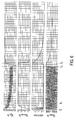
- Fig. 6 is a waveform diagram showing the waveforms of the gate-source voltage Vgs of the switch Q1, the sensed voltage Vsense, the discharging current I R3-P flowing from the filtering capacitor C1 through the bleeder resistor R3, and the voltage Vxcap across the filtering capacitor C1.
- Fig. 2 is a block diagram showing the discharge loop and the active control circuit thereof according to the invention.
- the power supply circuit includes a filtering capacitor Cx connected across the fire line and the neutral line of the input AC voltage Vin. That is, the filtering capacitor Cx is connected in parallel with the input side of the power supply circuit, in which the input AC voltage Vin is provided as the input voltage for the power supply circuit.
- the discharge loop of the invention includes a voltage sensing circuit 202 connected to the input side of the power supply circuit to detect the presence of the input AC voltage Vin.
- the discharge loop of the invention further includes a bleeder resistor Rb for providing a discharge path for the filtering capacitor Cx.
- the discharge loop of the invention further includes a switch circuit SW1 connected in series with the bleeder resistor Rb and connected to the voltage sensing circuit 202.
- the switch circuit SW1 is configured to control the discharging operation of the filtering capacitor Cx and the bleeder resistor Rb.
- the voltage sensing circuit 202 is configured to control the switching operation of the switch circuit SW1.
- the switch circuit SW1 and the voltage sensing circuit 202 constitute an active control circuit 206 for actively manipulating the switch circuit SW1 to turn on or off according to the status of the input AC voltage Vin as to whether the input AC voltage Vin is interrupted, thereby determining if the electric energy of the filtering capacitor Cx is allowable to be discharged through the bleeder resistor Rb.
- Fig. 3 is a circuit diagram showing a power supply circuit according to one embodiment of the invention, in which the filtering capacitor C1 and the bleeder resistor R3 are individually similar to the filtering capacitor Cx and the bleeder resistor Rb of Fig. 2 , and it is not intended to give details about the functionality of the filtering capacitor C1 and the bleeder resistor R3 herein.
- the power supply circuit of Fig. 3 includes a bridge rectifier consisted of rectifying diodes D5-D8 and connected to the input side of the power supply circuit for receiving the input AC voltage Vin and rectifying the input AC voltage Vin into a full-wave rectified DC voltage, in which the input end of the bridge rectifier D5-D8 is connected to the filtering capacitor C1.
- the full-wave rectified DC voltage outputted from the bridge rectifier D5-D8 is used to power a load Z L .
- the power supply circuit of Fig. 3 further includes an input bulk capacitor C4 connected in parallel between the positive output terminal and the negative output terminal of the bridge rectifier D5-D8 for removing the high-frequency ripples of the full-wave rectified DC voltage outputted from the bridge rectifier D5-D8.
- the power supply circuit further includes a reverse current protection circuit (D1, D2) connected between the input side of the power supply circuit and the bleeder resistor R3, i.e. connected in series with the bleeder resistor R3 for prohibiting a reverse current from flowing into the input side of the power supply circuit.
- the power supply circuit further a differentiator consisted of a resistor R1 and a capacitor C2 and connected to the input side of the power supply circuit for detecting the variation of the input AC voltage Vin.
- the power supply circuit further includes a half-wave rectifier consisted of rectifying diodes D3 and D4 and connected to the differentiator (R1, C2) and the gate of the switch Q1 for performing half-wave rectification to the detected AC voltage outputted from the differentiator (R1, C2), thereby outputting a half-wave rectified DC voltage.
- the switch Q1 is driven by the half-wave rectified DC voltage outputted from the half-wave rectifier (D3, D4) to turn on or off.
- the voltage level of the half-wave rectified DC voltage outputted from the half-wave rectifier (D3, D4) represents the voltage level of the input AC voltage Vin.
- the power supply circuit further includes a voltage clamp consisted of a zener diode ZD1 connected across the half-wave rectifier (D3, D4) for clamping the voltage level of the half-wave rectified DC voltage outputted from the half-wave rectifier (D3, D4) and protecting the switch Q1 from being damaged as a result of over-voltage conditions. It is noteworthy that the zener diode ZD1 is an optional element.
- one end of the zener diode ZD1 is connected to the half-wave rectifier and the gate of the switch Q1 and the other end of the zener diode ZD1 is connected to a common ground terminal (the negative output terminal of the bridge rectifier (D5-D8)).
- the power supply circuit further includes a filter consisted of the resistor R2 and the capacitor C3 and connected in parallel with the voltage clamp ZD1 and connected to the gate of the switch Q1 for removing the noises of half-wave rectified DC voltage outputted from the half-wave rectifier (D3, D4) at an unwanted frequency band, e.g. the AC voltage frequency band over 60Hz.
- the power supply circuit further includes a switch Q1 having a drain connected in series with the bleeder resistor R3, a gate connected to the half-wave rectifier (D3, D4), and a source connected to the common ground terminal.
- the switch Q1 may be implemented by a junction field-effect transistor (JFET), a metal-oxide-semiconductor field-effect transistor (MOSFET), or an isolated gate bipolar transistor (IGBT).
- JFET junction field-effect transistor
- MOSFET metal-oxide-semiconductor field-effect transistor
- IGBT isolated gate bipolar transistor
- the switch Q1 is allowed to be turned off if the driving voltage of the gate of the switch Q1 is a negative voltage.
- the the differentiator (R1, C2), the half-wave rectifier (D3, D4), the filter (R2, C3), and the voltage clamp ZD1 constitute the voltage sensing circuit 202 of Fig. 2 .
- the reverse current protection circuit (D1, D2) is required for proving a discharge path for the bleeder resistor R3 when it is connected to the AC voltage Vin.
- the switch Q1 constitutes the switch circuit SW1 of Fig. 2 .
- the operation of the active control circuit of Fig. 3 it will be elaborated in the following paragraphs.
- the current flows from the neutral line of the input AC voltage Vin through rectifying diode D8, load Z L , resistor R2, diode D4, resistor R1, and capacitor C2 and then flows back to the fire line of the input AC voltage Vin during the negative half cycle of the input AC voltage Vin.
- the current will charge the filtering capacitor C3 and thus a negative voltage is generated across the filtering capacitor C3 and filtered by the filtering capacitor C3. Therefore, the gate driving voltage of the switch Q1 is a negative voltage and the switch Q1 is turned off accordingly. Hence, no current will be flowing through the bleeder resistor R3 such that the bleeder resistor R3 will not consume power.
- the voltage clamp ZD1 can protect the gate of the switch Q1 from being damaged as a result of over-voltage conditions.
- the capacitor C2 is reset and the current flows from the fire line of the input AC voltage Vin through the capacitor C2, resistor R1, diode D3, rectifying diode D6 and then flows back to the neutral line of the input AC voltage Vin.
- the gate driving voltage of the switch Q1 i.e. the negative voltage across the filtering capacitor C3 is discharged through the resistor R2 until the negative voltage across the filtering capacitor C3 reaches the threshold voltage of the switch Q1. Under this condition, the switch Q1 is turned on.
- the filtering capacitor C1 will discharge toward the bleeder resistor R3 through the reverse current protection circuit (D1, D2).
- the voltage across the filtering capacitor C 1 can be either a positive voltage or a negative voltage.
- the polarity of the voltage across the filtering capacitor C1 depending on the phase of the input AC voltage Vin at the time the input AC voltage Vin is interrupted. If the voltage across the filtering capacitor C1 is a positive voltage, the energy stored in the filtering capacitor C1 is discharged through the diode D1, the bleeder resistor R3, the switch Q1, and the rectifying diode D6. If the voltage across the filtering capacitor C1 is a negative voltage, the energy stored in the filtering capacitor C1 is discharged through the diode D2, the bleeder resistor R3, the switch Q1, and the rectifying diode D5.
- Fig. 4A shows a modification of the circuitry of Fig. 3 .
- the circuitry of Fig. 4A removes the reverse current protection circuit (D1, D2), while the bleeder resistor for the filtering capacitor C1 is relocated at the output end of the bridge rectifier D5-D8 instead of the input end of the bridge rectifier D5-D8.
- the circuitry of Fig. 4A includes a bleeder resistor R4 located at the output end of the bridge rectifier D5-D8 and connected in parallel with the input bulk capacitor C4 and connected to the drain of the switch Q1. Therefore, the energy stored in the filtering capacitor C1 can be discharged through the rectifying diode D7 or the rectifying diode D8, the bleeder resistor R4, and the switch Q1.
- Fig. 4B shows another modification of the circuitry of Fig. 3 .
- the circuitry of Fig. 4B adds the bleeder resistor R4 of Fig. 4A located at the output end of bridge rectifier D5-D8 to the circuitry of Fig. 3 .
- the circuitry of Fig. 4B includes two bleeder resistors R3 and R4.
- the energy stored in the filtering capacitor C1 not only can be discharged through the rectifying diode D7 or the rectifying diode D8, the second bleeder resistor R4, and the switch Q1, but can be discharged through the diode D1 or the diode D2, the first bleeder resistor R3, the switch Q1, and the diode D5 or the diode D6.
- Fig. 5 shows a modification of the circuitry of Fig. 4B .
- the circuitry of Fig. 5 adds a monitoring circuit 502 to the circuitry of Fig. 4B for generating a sensed voltage Vsense indicative of the voltage level of the input AC voltage Vin.
- the monitoring circuit 502 includes a pair of serially-connected resistors R5 and R6 connected between the bleeder resistors R3 and R4 and the common ground terminal COM, and a filter consisted of a resistor R7 and a capacitor C5 and connected in series with the serially-connected resistors R5 and R6.
- the monitoring circuit 502 further includes a diode D9 connected between the serially-connected resistors R5 and R6 and the filter (R7, C5).
- the serially-connected resistors R5 and R6 function as a voltage divider being connected to the bleeder resistors R3 and R4 for generating a fractional voltage of the input AC voltage Vin.
- the fractional voltage generated by serially-connected resistors R5 and R6 is the sensed voltage Vsense indicative of the voltage level of the input AC voltage Vin. If the voltage drop of the bridge rectifier D5-D8 is ignored, the peak voltage of the sensed voltage Vsense can be calculated with the following equation:
- Vsense 1.414 x Vin x R ⁇ 5 / R ⁇ 3 + R ⁇ 6 + R ⁇ 5
- the sensed voltage Vsense will be provided for the housekeeping circuit (not shown) of the power supply system in order to allow the power supply system to realize the variation of the input AC voltage Vin.
- the filter (R7, C5) is used to remove the noises of sensed voltage Vsense at an unwanted frequency band, e.g. the AC voltage frequency band over 60Hz.
- the switch Q1 is turned on and the energy stored in the filtering capacitor C5 can be discharged through the resistor R7, the diode D9, and the switch Q1.
- Fig. 6 is a waveform diagram showing the waveforms of the gate-source voltage Vgs of the switch Q1, the sensed voltage Vsense, the discharging current I R3-P flowing from the filtering capacitor C1 through the bleeder resistor R3, and the voltage Vxcap across the filtering capacitor C1.
- the operation of the active control circuit of the invention will be further illustrated with reference to Fig. 6 .
- the power supply circuit is powered on, and the period of 0-t1 denotes the startup stage of the power supply circuit.
- the gate-source voltage Vgs of the switch Q1 gradually declines from 0 to -5V thereby turning off the switch Q1.
- the input AC voltage Vin of the power supply circuit gradually increases to its rated voltage level.
- the sensed voltage Vsense will gradually increase to a level indicative of a fractional voltage of the rated level of the input AC voltage Vin.
- the filtering capacitor C1 will not discharge through the bleeder resistor R3. Therefore, the discharging current I R3-P of the filtering capacitor C1 is zero.
- the filtering capacitor C1 is charged by a positive voltage in the positive half-cycle of the input AC voltage Vin and charged by a negative voltage in the negative half-cycle of the input AC voltage Vin.
- the voltage Vxcap across the filtering capacitor C1 is wavering between a positive voltage of, e.g. 300V and a negative voltage of, e.g. -300V.
- the period of t1-t2 denotes the power supplying stage of the power supply circuit.
- the input AC voltage Vin has been steadied at its rated level such that the power supply circuit can output a stable and regulated output voltage.
- the gate-source voltage Vgs of the switch Q1 is maintained at a level as lower than -6V, and the sensed voltage Vsense is maintained at a stable voltage level.
- the input AC voltage Vin is interrupted.
- the level of the input AC voltage Vin will maintained for a while and will start declining at the time point of t3.
- the level of the input AC voltage Vin is declined to zero.
- the gate-source voltage Vgs of the switch Q1 increases to be higher than the threshold voltage of the switch Q1, thereby turning on the switch Q1.
- the sensed voltage Vsense is gradually declined to zero.
- the filtering capacitor C1 starts the discharging operation through the bleeder resistor R3.
- the discharging current I R3-P starts to increase and declines to zero for a while to indicate the end of the discharging operation.
- the voltage Vxcap of the filtering capacitor C1 will gradually decline to zero.
- the invention provides an active control circuit for manipulating the discharge loop in a power supply circuit.
- the active control circuit is configured to manipulate the discharge loop in a power supply circuit in an active manner that prohibits that bleeder resistor of the power supply circuit from causing power loss as the input AC voltage of the power supply circuit is applying and provides a fast discharge path for the filtering capacitor in the power supply circuit to expedite the discharging operation.
- the active control circuit of the invention can lessen the power loss of the circuit and enhance the power efficiency of the circuit.
Landscapes
- Engineering & Computer Science (AREA)
- Power Engineering (AREA)
- Rectifiers (AREA)
- Inverter Devices (AREA)
Abstract
Provided is a discharge loop for power supply and the active control circuit thereof for actively regulating the discharging operation of the discharge loop of the power supply. The inventive active control circuit is able to disallow the current to flow through the bleeder resistor of the discharge loop to cause power loss when the input power of the power supply is applying, and provide a fast discharge path for the bleeder resistor to expedite the discharging operation when the input power of the power supply is interrupted. Therefore, the inventive active control circuit is able to reduce the power loss of the power supply and enhance the power efficiency of the power supply.
Description
- The present invention relates to a discharge loop for a power supply circuit, and more particularly to an active control circuit for a discharge loop in a power supply circuit.
- Capacitor is widely known as an indispensable electronic component for the purpose of power filtering and energy storage in power supply circuits, which convert an AC power such as utility power into a DC voltage tailored to power an electric appliance.
- Referring to
Fig. 1 , a discharge loop in a power supply circuit according to the prior art is shown. As shown inFig. 1 , the conventional power supply circuit 1 includes a filtering capacitor C connected in parallel with the input side of the power supply circuit for removing the high-frequency noises of the input AC voltage Vin, thereby reducing the electromagnetic interference induced during the operation phase of the power supply circuit. - Moreover, the safety regulations of electric appliance normally require the electric energy stored in the filtering capacitor C to be rapidly discharged down to 37% of its peak voltage as the power supply circuit is interrupted in receiving the input AC voltage Vin, thereby reducing the risk of suffering from electric shock as a result of the inadvertent contact of the power supply circuit. In order to meet the safety regulations, the conventional power supply circuit of
Fig. 1 includes a discharge loop consisted of a bleeder resistor R connected in parallel to the filtering capacitor C for providing a discharge path for the filtering capacitor C. As the power supply circuit is interrupted in receiving the input AC voltage Vin, the voltage of the filtering capacitor C is able to be discharged through the bleeder resistor R within a time period defined by the time constant which is derived from the multiplication the capacitance of the filtering capacitor C by the resistance of the bleeder resistor R, in order to comply with the standard prescribed by the safety regulations. - With the increasing of the power consumption of electric appliances, the capacitance of the filtering capacitor C and the power consumption of the power supply circuit increase as well. This would deflate the power efficiency of the power supply circuit.
- Therefore, the invention proposes an active control circuit for a discharge loop in a power supply circuit to reduce the power loss of the discharge loop and enhance the power efficiency of the power supply circuit.
- An object of the invention is to provide a discharge loop for a power supply circuit and an active control circuit thereof. The active control circuit manipulates the discharge loop to reduce the unnecessary power loss incurred with the discharge loop as the power supply circuit is operating with the input AC voltage, and manipulates the discharge loop to rapidly discharge the energy stored in the energy storage element of the power supply circuit as the input AC voltage of the power supply circuit is interrupted.
- The major aspect of the invention is attained by providing a discharge loop for a power supply circuit, in which the power supply circuit includes a filtering capacitor connected to an input side of the power supply circuit for removing the electromagnetic interference caused by the input AC voltage. The inventive discharge loop includes: (I) a first bleeder resistor connected to the filtering capacitor for allowing the energy stored in the filtering capacitor to be discharged therethrough as the input AC voltage is interrupted, and (II) an active control circuit connected to the first bleeder resistor and the input side of the power supply circuit for manipulating the discharge loop to discharge the energy of the filtering capacitor through the first bleeder resistor according to the status of the input AC voltage. The active control circuit includes: (I) a switch connected in series with the first bleeder resistor, and (II) a voltage sensing circuit connected to the input side of the power supply circuit and the control terminal of the switch for manipulating the switching operation of the switch. The voltage sensing circuit includes: (I) a differentiator connected to the input side of the power supply circuit for detecting the variation of the input AC voltage, and (II) a half-wave rectifier connected to the differentiator and the control terminal of the switch for performing half-wave rectification to the input AC voltage and generating a half-wave rectified DC voltage accordingly, thereby manipulating the switching operation of the switch.
- The minor aspect of the invention is attained by providing an active control circuit for use with a discharge loop of a power supply circuit. The power supply circuit includes a filtering capacitor connected to the input side of the power supply circuit for removing the electromagnetic interference on the input AC voltage of the power supply circuit. The discharge loop includes: (I) a first bleeder resistor connected to the filtering capacitor for allowing the energy stored in the filtering capacitor to be discharged therethrough as the input AC voltage is interrupted. The active control circuit includes: (I) a switch connected in series with the first bleeder resistor, and (II) a voltage sensing circuit connected to the input side of the power supply circuit and the control terminal of the switch for manipulating the switching operation of the switch. The voltage sensing circuit includes: (I) a differentiator connected to the input side of the power supply circuit for detecting the variation of the input AC voltage, and (II) a half-wave rectifier connected to the differentiator and the control terminal of the switch for performing half-wave rectification to the input AC voltage and generating a half-wave rectified DC voltage accordingly, thereby manipulating the switching operation of the switch.
- Now the foregoing and other features and advantages of the present invention will be best understood through the following descriptions with reference to the accompanying drawings, wherein:
-
Fig. 1 is a circuit diagram showing a discharge loop in a power supply circuit according to the prior art; -
Fig. 2 is a circuit diagram showing a discharge loop in a power supply circuit and an active control circuit thereof according to one embodiment of the invention; -
Fig. 3 is a circuit diagram showing a power supply circuit incorporating a discharge loop and an active control circuit for manipulating the discharge loop according to one embodiment of the invention; -
Fig. 4A shows a modification of the circuitry ofFig. 3 ; -
Fig. 4B shows another modification of the circuitry ofFig. 3 ; -
Fig. 5 shows a modification of the circuitry ofFig. 4B ; and -
Fig. 6 is a waveform diagram showing the waveforms of the gate-source voltage Vgs of the switch Q1, the sensed voltage Vsense, the discharging current IR3-P flowing from the filtering capacitor C1 through the bleeder resistor R3, and the voltage Vxcap across the filtering capacitor C1. - Several preferred embodiments embodying the features and advantages of the invention will be expounded in following paragraphs of descriptions. It is to be realized that the present invention is allowed to have various modification in different respects, all of which are without departing from the scope of the present invention, and the description herein and the drawings are to be taken as illustrative in nature, but not to be taken as a confinement for the invention.
-
Fig. 2 is a block diagram showing the discharge loop and the active control circuit thereof according to the invention. InFig. 2 , the power supply circuit includes a filtering capacitor Cx connected across the fire line and the neutral line of the input AC voltage Vin. That is, the filtering capacitor Cx is connected in parallel with the input side of the power supply circuit, in which the input AC voltage Vin is provided as the input voltage for the power supply circuit. The discharge loop of the invention includes avoltage sensing circuit 202 connected to the input side of the power supply circuit to detect the presence of the input AC voltage Vin. The discharge loop of the invention further includes a bleeder resistor Rb for providing a discharge path for the filtering capacitor Cx. The functionality of the filtering capacitor Cx and the bleeder resistor Rb is similar to that of the filtering capacitor C and the bleeder resistor R ofFig. 1 , and thus it is not intended to give details of the functionality of the filtering capacitor Cx and the bleeder resistor Rb herein. It is noteworthy that the discharge loop of the invention further includes a switch circuit SW1 connected in series with the bleeder resistor Rb and connected to thevoltage sensing circuit 202. The switch circuit SW1 is configured to control the discharging operation of the filtering capacitor Cx and the bleeder resistor Rb. Thevoltage sensing circuit 202 is configured to control the switching operation of the switch circuit SW1. The switch circuit SW1 and thevoltage sensing circuit 202 constitute anactive control circuit 206 for actively manipulating the switch circuit SW1 to turn on or off according to the status of the input AC voltage Vin as to whether the input AC voltage Vin is interrupted, thereby determining if the electric energy of the filtering capacitor Cx is allowable to be discharged through the bleeder resistor Rb. -
Fig. 3 is a circuit diagram showing a power supply circuit according to one embodiment of the invention, in which the filtering capacitor C1 and the bleeder resistor R3 are individually similar to the filtering capacitor Cx and the bleeder resistor Rb ofFig. 2 , and it is not intended to give details about the functionality of the filtering capacitor C1 and the bleeder resistor R3 herein. The power supply circuit ofFig. 3 includes a bridge rectifier consisted of rectifying diodes D5-D8 and connected to the input side of the power supply circuit for receiving the input AC voltage Vin and rectifying the input AC voltage Vin into a full-wave rectified DC voltage, in which the input end of the bridge rectifier D5-D8 is connected to the filtering capacitor C1. The full-wave rectified DC voltage outputted from the bridge rectifier D5-D8 is used to power a load ZL. The power supply circuit ofFig. 3 further includes an input bulk capacitor C4 connected in parallel between the positive output terminal and the negative output terminal of the bridge rectifier D5-D8 for removing the high-frequency ripples of the full-wave rectified DC voltage outputted from the bridge rectifier D5-D8. The power supply circuit further includes a reverse current protection circuit (D1, D2) connected between the input side of the power supply circuit and the bleeder resistor R3, i.e. connected in series with the bleeder resistor R3 for prohibiting a reverse current from flowing into the input side of the power supply circuit. The power supply circuit further a differentiator consisted of a resistor R1 and a capacitor C2 and connected to the input side of the power supply circuit for detecting the variation of the input AC voltage Vin. The power supply circuit further includes a half-wave rectifier consisted of rectifying diodes D3 and D4 and connected to the differentiator (R1, C2) and the gate of the switch Q1 for performing half-wave rectification to the detected AC voltage outputted from the differentiator (R1, C2), thereby outputting a half-wave rectified DC voltage. The switch Q1 is driven by the half-wave rectified DC voltage outputted from the half-wave rectifier (D3, D4) to turn on or off. The voltage level of the half-wave rectified DC voltage outputted from the half-wave rectifier (D3, D4) represents the voltage level of the input AC voltage Vin. The power supply circuit further includes a voltage clamp consisted of a zener diode ZD1 connected across the half-wave rectifier (D3, D4) for clamping the voltage level of the half-wave rectified DC voltage outputted from the half-wave rectifier (D3, D4) and protecting the switch Q1 from being damaged as a result of over-voltage conditions. It is noteworthy that the zener diode ZD1 is an optional element. In the instant embodiment, one end of the zener diode ZD1 is connected to the half-wave rectifier and the gate of the switch Q1 and the other end of the zener diode ZD1 is connected to a common ground terminal (the negative output terminal of the bridge rectifier (D5-D8)). The power supply circuit further includes a filter consisted of the resistor R2 and the capacitor C3 and connected in parallel with the voltage clamp ZD1 and connected to the gate of the switch Q1 for removing the noises of half-wave rectified DC voltage outputted from the half-wave rectifier (D3, D4) at an unwanted frequency band, e.g. the AC voltage frequency band over 60Hz. The power supply circuit further includes a switch Q1 having a drain connected in series with the bleeder resistor R3, a gate connected to the half-wave rectifier (D3, D4), and a source connected to the common ground terminal. The switch Q1 may be implemented by a junction field-effect transistor (JFET), a metal-oxide-semiconductor field-effect transistor (MOSFET), or an isolated gate bipolar transistor (IGBT). The switch Q1 is allowed to be turned off if the driving voltage of the gate of the switch Q1 is a negative voltage. The the differentiator (R1, C2), the half-wave rectifier (D3, D4), the filter (R2, C3), and the voltage clamp ZD1 constitute thevoltage sensing circuit 202 ofFig. 2 . The reverse current protection circuit (D1, D2) is required for proving a discharge path for the bleeder resistor R3 when it is connected to the AC voltage Vin. The switch Q1 constitutes the switch circuit SW1 ofFig. 2 . As to the operation of the active control circuit ofFig. 3 , it will be elaborated in the following paragraphs. - When the input AC voltage Vin is applying to the power supply circuit, the current flows from the neutral line of the input AC voltage Vin through rectifying diode D8, load ZL, resistor R2, diode D4, resistor R1, and capacitor C2 and then flows back to the fire line of the input AC voltage Vin during the negative half cycle of the input AC voltage Vin. Under this condition, the current will charge the filtering capacitor C3 and thus a negative voltage is generated across the filtering capacitor C3 and filtered by the filtering capacitor C3. Therefore, the gate driving voltage of the switch Q1 is a negative voltage and the switch Q1 is turned off accordingly. Hence, no current will be flowing through the bleeder resistor R3 such that the bleeder resistor R3 will not consume power. The voltage clamp ZD1 can protect the gate of the switch Q1 from being damaged as a result of over-voltage conditions. During the positive half-cycle of the input AC voltage Vin, the capacitor C2 is reset and the current flows from the fire line of the input AC voltage Vin through the capacitor C2, resistor R1, diode D3, rectifying diode D6 and then flows back to the neutral line of the input AC voltage Vin. When the input AC voltage Vin is interrupted, the current flowing through the capacitor C2 is terminated. In the meantime, the gate driving voltage of the switch Q1, i.e. the negative voltage across the filtering capacitor C3 is discharged through the resistor R2 until the negative voltage across the filtering capacitor C3 reaches the threshold voltage of the switch Q1. Under this condition, the switch Q1 is turned on. In the meantime, the filtering capacitor C1 will discharge toward the bleeder resistor R3 through the reverse current protection circuit (D1, D2). Besides, when the filtering capacitor C1 is about to discharge, the voltage across the filtering capacitor C 1 can be either a positive voltage or a negative voltage. The polarity of the voltage across the filtering capacitor C1 depending on the phase of the input AC voltage Vin at the time the input AC voltage Vin is interrupted. If the voltage across the filtering capacitor C1 is a positive voltage, the energy stored in the filtering capacitor C1 is discharged through the diode D1, the bleeder resistor R3, the switch Q1, and the rectifying diode D6. If the voltage across the filtering capacitor C1 is a negative voltage, the energy stored in the filtering capacitor C1 is discharged through the diode D2, the bleeder resistor R3, the switch Q1, and the rectifying diode D5.
-
Fig. 4A shows a modification of the circuitry ofFig. 3 . Compared toFig. 3 , the circuitry ofFig. 4A removes the reverse current protection circuit (D1, D2), while the bleeder resistor for the filtering capacitor C1 is relocated at the output end of the bridge rectifier D5-D8 instead of the input end of the bridge rectifier D5-D8. As shown, the circuitry ofFig. 4A includes a bleeder resistor R4 located at the output end of the bridge rectifier D5-D8 and connected in parallel with the input bulk capacitor C4 and connected to the drain of the switch Q1. Therefore, the energy stored in the filtering capacitor C1 can be discharged through the rectifying diode D7 or the rectifying diode D8, the bleeder resistor R4, and the switch Q1. -
Fig. 4B shows another modification of the circuitry ofFig. 3 . Compared toFig. 3 , the circuitry ofFig. 4B adds the bleeder resistor R4 ofFig. 4A located at the output end of bridge rectifier D5-D8 to the circuitry ofFig. 3 . As shown, the circuitry ofFig. 4B includes two bleeder resistors R3 and R4. Therefore, the energy stored in the filtering capacitor C1 not only can be discharged through the rectifying diode D7 or the rectifying diode D8, the second bleeder resistor R4, and the switch Q1, but can be discharged through the diode D1 or the diode D2, the first bleeder resistor R3, the switch Q1, and the diode D5 or the diode D6. -
Fig. 5 shows a modification of the circuitry ofFig. 4B . Compared toFig. 4B , the circuitry ofFig. 5 adds amonitoring circuit 502 to the circuitry ofFig. 4B for generating a sensed voltage Vsense indicative of the voltage level of the input AC voltage Vin. Themonitoring circuit 502 includes a pair of serially-connected resistors R5 and R6 connected between the bleeder resistors R3 and R4 and the common ground terminal COM, and a filter consisted of a resistor R7 and a capacitor C5 and connected in series with the serially-connected resistors R5 and R6. Themonitoring circuit 502 further includes a diode D9 connected between the serially-connected resistors R5 and R6 and the filter (R7, C5). The serially-connected resistors R5 and R6 function as a voltage divider being connected to the bleeder resistors R3 and R4 for generating a fractional voltage of the input AC voltage Vin. The fractional voltage generated by serially-connected resistors R5 and R6 is the sensed voltage Vsense indicative of the voltage level of the input AC voltage Vin. If the voltage drop of the bridge rectifier D5-D8 is ignored, the peak voltage of the sensed voltage Vsense can be calculated with the following equation: -

- The sensed voltage Vsense will be provided for the housekeeping circuit (not shown) of the power supply system in order to allow the power supply system to realize the variation of the input AC voltage Vin. The filter (R7, C5) is used to remove the noises of sensed voltage Vsense at an unwanted frequency band, e.g. the AC voltage frequency band over 60Hz. When the input AC voltage Vin is interrupted, the switch Q1 is turned on and the energy stored in the filtering capacitor C5 can be discharged through the resistor R7, the diode D9, and the switch Q1.
-
Fig. 6 is a waveform diagram showing the waveforms of the gate-source voltage Vgs of the switch Q1, the sensed voltage Vsense, the discharging current IR3-P flowing from the filtering capacitor C1 through the bleeder resistor R3, and the voltage Vxcap across the filtering capacitor C1. Now the operation of the active control circuit of the invention will be further illustrated with reference toFig. 6 . At the time point of 0, the power supply circuit is powered on, and the period of 0-t1 denotes the startup stage of the power supply circuit. During this period, the gate-source voltage Vgs of the switch Q1 gradually declines from 0 to -5V thereby turning off the switch Q1. The input AC voltage Vin of the power supply circuit gradually increases to its rated voltage level. Therefore, the sensed voltage Vsense will gradually increase to a level indicative of a fractional voltage of the rated level of the input AC voltage Vin. As the switch Q1 is turned off, the filtering capacitor C1 will not discharge through the bleeder resistor R3. Therefore, the discharging current IR3-P of the filtering capacitor C1 is zero. The filtering capacitor C1 is charged by a positive voltage in the positive half-cycle of the input AC voltage Vin and charged by a negative voltage in the negative half-cycle of the input AC voltage Vin. As a result, the voltage Vxcap across the filtering capacitor C1 is wavering between a positive voltage of, e.g. 300V and a negative voltage of, e.g. -300V. The period of t1-t2 denotes the power supplying stage of the power supply circuit. During the period of t1-t2, the input AC voltage Vin has been steadied at its rated level such that the power supply circuit can output a stable and regulated output voltage. During this period, the gate-source voltage Vgs of the switch Q1 is maintained at a level as lower than -6V, and the sensed voltage Vsense is maintained at a stable voltage level. At the time point of t2, the input AC voltage Vin is interrupted. Though the input AC voltage Vin has been interrupted, the level of the input AC voltage Vin will maintained for a while and will start declining at the time point of t3. At the time point of t3, the level of the input AC voltage Vin is declined to zero. In the meantime, the gate-source voltage Vgs of the switch Q1 increases to be higher than the threshold voltage of the switch Q1, thereby turning on the switch Q1. The sensed voltage Vsense is gradually declined to zero. As the switch Q1 is turned on, the filtering capacitor C1 starts the discharging operation through the bleeder resistor R3. Hence, the discharging current IR3-P starts to increase and declines to zero for a while to indicate the end of the discharging operation. Also, the voltage Vxcap of the filtering capacitor C1 will gradually decline to zero. - In conclusion, the invention provides an active control circuit for manipulating the discharge loop in a power supply circuit. The active control circuit is configured to manipulate the discharge loop in a power supply circuit in an active manner that prohibits that bleeder resistor of the power supply circuit from causing power loss as the input AC voltage of the power supply circuit is applying and provides a fast discharge path for the filtering capacitor in the power supply circuit to expedite the discharging operation. Thus, the active control circuit of the invention can lessen the power loss of the circuit and enhance the power efficiency of the circuit.
- While the present invention has been described in terms of what are presently considered to be the most practical and preferred embodiments, it is to be understood that the present invention need not be restricted to the disclosed embodiment. On the contrary, it is intended to cover various modifications and similar arrangements included within the spirit and scope of the appended claims which are to be accorded with the broadest interpretation so as to encompass all such modifications and similar structures. Therefore, the above description and illustration should not be taken as limiting the scope of the present invention which is defined by the appended claims.
Claims (16)
- A discharge loop for a power supply circuit having a filtering capacitor connected to an input side of the power supply circuit for removing electromagnetic interference caused by an input AC voltage, the discharge loop comprising:a first bleeder resistor connected to the filtering capacitor for allowing energy stored in the filtering capacitor to be discharged therethrough when the input AC voltage is interrupted; andan active control circuit connected to the first bleeder resistor and the input side of the power supply circuit for manipulating the discharge loop according to a status of the input AC voltage to regulate the discharging operation of the energy stored in the filtering capacitor through the first bleeder resistor, the active control circuit comprising:a switch connected in series with the first bleeder resistor; anda voltage sensing circuit connected to the input side of the power supply circuit and a control terminal of the switch for manipulating the switching operation of the switch, the voltage sensing circuit comprising:a differentiator connected to the input side of the power supply circuit for detecting a variation of the input AC voltage; anda half-wave rectifier connected to the differentiator and the control terminal of the switch for performing half-wave rectification to the input AC voltage to generate a half-wave rectified DC voltage, thereby driving the switch.
- The discharge loop according to claim 1 wherein the voltage sensing circuit further includes a reverse current protection circuit connected in series with the first bleeder resistor for prohibiting a reverse current from flowing into the input side of the power supply circuit.
- The discharge loop according to claim 1 wherein the reverse current protection circuit includes a pair of diodes.
- The discharge loop according to claim 1 wherein the voltage sensing circuit further includes a voltage clamp having one end connected to the half-wave rectifier and the control terminal of the switch and the other end connected to a common ground terminal for clamping the half-wave rectified DC voltage and protecting the switch from being damaged as a result of over-voltage conditions.
- The discharge loop according to claim 4 wherein the voltage clamp includes a zener diode.
- The discharge loop according to claim 1 wherein the voltage sensing circuit further includes a filter connected to the control terminal of the switch for removing noises from the half-wave rectified DC voltage.
- The discharge loop according to claim 6 wherein the filter includes a resistor and a capacitor.
- The discharge loop according to claim 1 wherein the power supply circuit further includes a bridge rectifier connected to the input side of the power supply circuit, and the first bleeder resistor is located at an input end of the bridge rectifier.
- The discharge loop according to claim 8 further comprising a second bleeder resistor located at an output end of the bridge rectifier.
- The discharge loop according to claim 9 further comprising a monitoring circuit connected in series with the second bleeder resistor and connected to the switch for sensing the input AC voltage and generating a sensed voltage indicative of a voltage level of the input AC voltage accordingly.
- The discharge loop according to claim 10 wherein the monitoring circuit includes:a voltage divider connected to the first bleeder resistor and the second bleeder resistor for generating a fractional voltage indicative of a fraction of the input AC voltage;a filter connected to the voltage divider for removing noises from the fractional voltage; anda diode connected between the voltage divider and the filter.
- The discharge loop according to claim 1 wherein the power supply circuit further includes a bridge rectifier connected to the input side of the power supply circuit, and the first bleeder resistor is located at an output end of the bridge rectifier.
- The discharge loop according to claim 1 wherein the switch comprises a junction field-effect transistor, a metal-oxide-semiconductor field-effect transistor, or an isolated gate bipolar transistor.
- An active control circuit for use with a discharge loop in a power supply circuit, wherein the power supply circuit comprises a filtering capacitor connected to an input side of the power supply circuit for removing electromagnetic interference caused by an input AC voltage and the discharge loop comprises a first bleeder resistor connected to the filtering capacitor for allowing the energy stored in the filtering capacitor to be discharged therethrough as the input AC voltage is interrupted, the active control circuit comprising:a switch connected in series with the first bleeder resistor; anda voltage sensing circuit connected to the input side of the power supply circuit and a control terminal of the switch for manipulate the switching operation of the switch, the voltage sensing circuit comprising:a differentiator connected to the input side of the power supply circuit for detecting variations of the input AC voltage;a half-wave rectifier connected to the differentiator and the control terminal of the switch for performing half-wave rectification to the input AC voltage to generate a half-wave rectified DC voltage, thereby driving the switch; anda filter connected to the control terminal of the switch for removing noises from the half-wave rectified DC voltage.
- The active control circuit according to claim 14 wherein the voltage sensing circuit further includes a reverse current protection circuit comprising a pair of diodes and connected in series with the first bleeder for prohibiting a reverse current from flowing into the input side of the power supply circuit.
- The active control circuit according to claim 14 wherein the voltage sensing circuit further includes a voltage clamp comprising a zener diode having one end connected to the half-wave rectifier and the control terminal of the switch and the other end connected to a common ground terminal for clamping the half-wave rectified DC voltage and protecting the switch from being damaged as a result of over-voltage conditions.
Applications Claiming Priority (1)
| Application Number | Priority Date | Filing Date | Title |
|---|---|---|---|
| CN2010102251487A CN102332835B (en) | 2010-07-12 | 2010-07-12 | Discharge circuit of power supply circuit and its active control circuit |
Publications (1)
| Publication Number | Publication Date |
|---|---|
| EP2408094A2 true EP2408094A2 (en) | 2012-01-18 |
Family
ID=44860191
Family Applications (1)
| Application Number | Title | Priority Date | Filing Date |
|---|---|---|---|
| EP11001093A Withdrawn EP2408094A2 (en) | 2010-07-12 | 2011-02-10 | Discharge loop for power supply circuit and active control circuit thereof |
Country Status (3)
| Country | Link |
|---|---|
| US (1) | US8406023B2 (en) |
| EP (1) | EP2408094A2 (en) |
| CN (1) | CN102332835B (en) |
Cited By (3)
| Publication number | Priority date | Publication date | Assignee | Title |
|---|---|---|---|---|
| WO2014021474A3 (en) * | 2012-08-01 | 2014-06-12 | Canon Kabushiki Kaisha | Power supply apparatus and image forming apparatus |
| EP2987240A4 (en) * | 2013-04-17 | 2016-12-21 | Otis Elevator Co | Drive unit employing gallium nitride switches |
| EP2624422A3 (en) * | 2012-01-31 | 2018-03-28 | Canon Kabushiki Kaisha | Power source, power failure detection apparatus, and image forming apparatus |
Families Citing this family (22)
| Publication number | Priority date | Publication date | Assignee | Title |
|---|---|---|---|---|
| JPWO2012105112A1 (en) * | 2011-02-04 | 2014-07-03 | 三菱電機株式会社 | DC / DC converter |
| JP5734689B2 (en) * | 2011-02-07 | 2015-06-17 | ミネベア株式会社 | Power circuit |
| US9590495B2 (en) | 2011-08-26 | 2017-03-07 | Futurewei Technologies, Inc. | Holdup time circuit and method for bridgeless PFC converter |
| CN103580461B (en) * | 2012-08-09 | 2016-03-30 | 艾默生网络能源有限公司 | A kind of power supply exports discharge circuit |
| TWI479764B (en) * | 2012-12-17 | 2015-04-01 | Niko Semiconductor Co Ltd | Low power bleeder circuit and ac converter having the same |
| CN103872887B (en) * | 2012-12-17 | 2017-04-12 | 尼克森微电子股份有限公司 | Low-power bleeder circuit and AC conversion system with low-power bleeder circuit |
| CN105027376B (en) * | 2013-03-15 | 2018-01-26 | 电力集成公司 | Rectifier with indicator switch |
| CN103236787B (en) * | 2013-04-12 | 2015-07-08 | 矽力杰半导体技术(杭州)有限公司 | Capacity discharge method and circuit |
| US9582054B2 (en) * | 2013-06-17 | 2017-02-28 | System General Corp. | Method and apparatus for selecting the output of programmable power adapter |
| CN105705221B (en) * | 2013-09-16 | 2018-09-14 | 株式会社Lg化学 | Water treatment separation membrane comprising ion-exchangeable polymer layer and method for forming same |
| TWI523383B (en) * | 2013-11-27 | 2016-02-21 | 台灣快捷國際股份有限公司 | Discharge circuits |
| TWI511433B (en) | 2013-12-20 | 2015-12-01 | Niko Semiconductor Co Ltd | Power conversion apparatus and control chip thereof |
| CN104734478B (en) * | 2013-12-20 | 2017-10-27 | 尼克森微电子股份有限公司 | power conversion device and control chip thereof |
| US9608538B2 (en) * | 2014-12-19 | 2017-03-28 | Distech Controls Inc. | Common zero volt reference AC / DC power supply with positive and negative rectification and method of operation thereof |
| CN204376693U (en) * | 2015-01-07 | 2015-06-03 | 江门博凯灯饰有限公司 | A kind of AC-DC power supply adaptor exported with AC |
| CN104980011B (en) * | 2015-06-26 | 2017-12-15 | 深圳科士达科技股份有限公司 | A kind of method for reducing bus capacitor ripple |
| CN105245215B (en) * | 2015-08-03 | 2017-12-15 | 中国农业大学 | A kind of ON-OFF control circuit and self-powered circuit |
| JP6611530B2 (en) * | 2015-09-11 | 2019-11-27 | キヤノン株式会社 | Power supply apparatus and image forming apparatus |
| CN109039037A (en) * | 2018-06-21 | 2018-12-18 | 许继电源有限公司 | A kind of high voltage direct current filter |
| CN111245211B (en) * | 2020-01-19 | 2021-08-13 | 东方电气自动控制工程有限公司 | Servo bleeder resistor intelligent control algorithm |
| CN112234812A (en) * | 2020-09-27 | 2021-01-15 | 杭州长川科技股份有限公司 | Bleeder circuit, energy storage circuit, semiconductor test system and bleeder method |
| CN114123114B (en) * | 2021-10-12 | 2025-08-08 | 维沃移动通信有限公司 | Discharge circuit control method and device, discharge device and electronic equipment |
Family Cites Families (5)
| Publication number | Priority date | Publication date | Assignee | Title |
|---|---|---|---|---|
| JP3987949B2 (en) * | 2001-02-26 | 2007-10-10 | サンケン電気株式会社 | AC / DC converter circuit |
| TWI258262B (en) * | 2004-05-10 | 2006-07-11 | Delta Electronics Inc | Power detection circuit capable of reducing power consumption under standby state |
| TWM329290U (en) * | 2007-10-09 | 2008-03-21 | Hipro Electronics Taiwan Co Ltd | Single stage power factor calibrating circuitry |
| US8461915B2 (en) * | 2009-06-03 | 2013-06-11 | System General Corp. | Start-up circuit to discharge EMI filter for power saving of power supplies |
| CN102075098B (en) * | 2009-11-25 | 2013-05-08 | 台达电子工业股份有限公司 | Capacitive energy discharge circuit capable of reducing power loss and its power supply circuit |
-
2010
- 2010-07-12 CN CN2010102251487A patent/CN102332835B/en not_active Expired - Fee Related
-
2011
- 2011-01-31 US US13/017,971 patent/US8406023B2/en not_active Expired - Fee Related
- 2011-02-10 EP EP11001093A patent/EP2408094A2/en not_active Withdrawn
Non-Patent Citations (1)
| Title |
|---|
| None |
Cited By (6)
| Publication number | Priority date | Publication date | Assignee | Title |
|---|---|---|---|---|
| EP2624422A3 (en) * | 2012-01-31 | 2018-03-28 | Canon Kabushiki Kaisha | Power source, power failure detection apparatus, and image forming apparatus |
| WO2014021474A3 (en) * | 2012-08-01 | 2014-06-12 | Canon Kabushiki Kaisha | Power supply apparatus and image forming apparatus |
| KR20150038140A (en) * | 2012-08-01 | 2015-04-08 | 캐논 가부시끼가이샤 | Power supply apparatus and image forming apparatus |
| CN104508964A (en) * | 2012-08-01 | 2015-04-08 | 佳能株式会社 | Power supply unit and image forming unit |
| US9274491B2 (en) | 2012-08-01 | 2016-03-01 | Canon Kabushiki Kaisha | Power supply apparatus and image forming apparatus |
| EP2987240A4 (en) * | 2013-04-17 | 2016-12-21 | Otis Elevator Co | Drive unit employing gallium nitride switches |
Also Published As
| Publication number | Publication date |
|---|---|
| CN102332835B (en) | 2013-12-04 |
| CN102332835A (en) | 2012-01-25 |
| US8406023B2 (en) | 2013-03-26 |
| US20120008354A1 (en) | 2012-01-12 |
Similar Documents
| Publication | Publication Date | Title |
|---|---|---|
| US8406023B2 (en) | Discharge loop for power supply circuit and active control circuit thereof | |
| CN107800283B (en) | Active clamp flyback controller and power supply system and control method thereof | |
| US8339055B2 (en) | Inrush current limiter for an LED driver | |
| CN103081322B (en) | Power control circuit and dump detection method | |
| CN111181426B (en) | Boost converter circuit and method of controlling transistor switches in the circuit | |
| EP3001779A1 (en) | Apparatus for driving light emitting diode | |
| KR20210028363A (en) | Power transforming apparatus having thermal protection function | |
| EP3182572B1 (en) | Electronic circuit and method for operating an electronic circuit | |
| CN103765752B (en) | DC power supply unit | |
| CN105027376B (en) | Rectifier with indicator switch | |
| JP2017216086A (en) | Lighting device and lighting apparatus | |
| US20180027619A1 (en) | Arcing protector | |
| KR102266356B1 (en) | Power converting device with function for protection circuit and totem-pole pfc | |
| US9246379B1 (en) | Current limit protection circuits for use with depletion MOSFET | |
| WO2024108979A1 (en) | Voltage control method and apparatus, and household appliance, storage medium and program | |
| JPH07231650A (en) | Boosting chopper circuit | |
| KR101873764B1 (en) | Power transforming apparatus and air conditioner including the same | |
| JP5803004B2 (en) | LED lighting device | |
| JP4832277B2 (en) | Power supply | |
| KR102189448B1 (en) | Power conversion apparatus of detecting hardware fault | |
| JP2011101571A (en) | Ac-dc converter | |
| KR102108071B1 (en) | Power transforming apparatus and air conditioner including the same | |
| KR101978223B1 (en) | Power transforming apparatus and air conditioner including the same | |
| JP6685018B2 (en) | Lighting device and lighting equipment | |
| KR102036112B1 (en) | Power supply apparatus and air conditioner including the same |
Legal Events
| Date | Code | Title | Description |
|---|---|---|---|
| 17P | Request for examination filed |
Effective date: 20110210 |
|
| AK | Designated contracting states |
Kind code of ref document: A2 Designated state(s): AL AT BE BG CH CY CZ DE DK EE ES FI FR GB GR HR HU IE IS IT LI LT LU LV MC MK MT NL NO PL PT RO RS SE SI SK SM TR |
|
| AX | Request for extension of the european patent |
Extension state: BA ME |
|
| PUAI | Public reference made under article 153(3) epc to a published international application that has entered the european phase |
Free format text: ORIGINAL CODE: 0009012 |
|
| STAA | Information on the status of an ep patent application or granted ep patent |
Free format text: STATUS: THE APPLICATION IS DEEMED TO BE WITHDRAWN |
|
| 18D | Application deemed to be withdrawn |
Effective date: 20160901 |