EP2408064A1 - Drahtlose integrierte Schaltung - Google Patents
Drahtlose integrierte Schaltung Download PDFInfo
- Publication number
- EP2408064A1 EP2408064A1 EP11185009A EP11185009A EP2408064A1 EP 2408064 A1 EP2408064 A1 EP 2408064A1 EP 11185009 A EP11185009 A EP 11185009A EP 11185009 A EP11185009 A EP 11185009A EP 2408064 A1 EP2408064 A1 EP 2408064A1
- Authority
- EP
- European Patent Office
- Prior art keywords
- wireless
- feeder circuit
- inductance elements
- feeder
- electrode
- Prior art date
- Legal status (The legal status is an assumption and is not a legal conclusion. Google has not performed a legal analysis and makes no representation as to the accuracy of the status listed.)
- Granted
Links
- 230000005855 radiation Effects 0.000 claims abstract description 157
- 230000005540 biological transmission Effects 0.000 claims abstract description 13
- 239000004020 conductor Substances 0.000 description 42
- 239000000758 substrate Substances 0.000 description 27
- 238000010586 diagram Methods 0.000 description 16
- 230000008878 coupling Effects 0.000 description 11
- 238000010168 coupling process Methods 0.000 description 11
- 238000005859 coupling reaction Methods 0.000 description 11
- 230000000694 effects Effects 0.000 description 11
- 229910052751 metal Inorganic materials 0.000 description 11
- 239000002184 metal Substances 0.000 description 11
- 239000000919 ceramic Substances 0.000 description 8
- 239000003989 dielectric material Substances 0.000 description 8
- 239000000696 magnetic material Substances 0.000 description 8
- 230000006870 function Effects 0.000 description 6
- 239000011347 resin Substances 0.000 description 6
- 229920005989 resin Polymers 0.000 description 6
- 239000003990 capacitor Substances 0.000 description 5
- 238000004891 communication Methods 0.000 description 5
- 238000010304 firing Methods 0.000 description 5
- 238000004519 manufacturing process Methods 0.000 description 5
- 239000000853 adhesive Substances 0.000 description 4
- 230000001070 adhesive effect Effects 0.000 description 4
- 238000007747 plating Methods 0.000 description 4
- 230000004044 response Effects 0.000 description 4
- 238000013461 design Methods 0.000 description 3
- 239000007769 metal material Substances 0.000 description 3
- 238000012546 transfer Methods 0.000 description 3
- 238000000034 method Methods 0.000 description 2
- 230000008569 process Effects 0.000 description 2
- 229910000859 α-Fe Inorganic materials 0.000 description 2
- 229920000106 Liquid crystal polymer Polymers 0.000 description 1
- 239000004977 Liquid-crystal polymers (LCPs) Substances 0.000 description 1
- 239000004642 Polyimide Substances 0.000 description 1
- 229910000831 Steel Inorganic materials 0.000 description 1
- 229910052782 aluminium Inorganic materials 0.000 description 1
- XAGFODPZIPBFFR-UHFFFAOYSA-N aluminium Chemical compound [Al] XAGFODPZIPBFFR-UHFFFAOYSA-N 0.000 description 1
- 230000003321 amplification Effects 0.000 description 1
- 230000015572 biosynthetic process Effects 0.000 description 1
- 230000006698 induction Effects 0.000 description 1
- 238000012986 modification Methods 0.000 description 1
- 230000004048 modification Effects 0.000 description 1
- 238000003199 nucleic acid amplification method Methods 0.000 description 1
- 229920001721 polyimide Polymers 0.000 description 1
- 238000012545 processing Methods 0.000 description 1
- 230000008054 signal transmission Effects 0.000 description 1
- 239000010959 steel Substances 0.000 description 1
- 238000004804 winding Methods 0.000 description 1
Images


Classifications
-
- G—PHYSICS
- G06—COMPUTING; CALCULATING OR COUNTING
- G06K—GRAPHICAL DATA READING; PRESENTATION OF DATA; RECORD CARRIERS; HANDLING RECORD CARRIERS
- G06K19/00—Record carriers for use with machines and with at least a part designed to carry digital markings
- G06K19/06—Record carriers for use with machines and with at least a part designed to carry digital markings characterised by the kind of the digital marking, e.g. shape, nature, code
- G06K19/067—Record carriers with conductive marks, printed circuits or semiconductor circuit elements, e.g. credit or identity cards also with resonating or responding marks without active components
- G06K19/07—Record carriers with conductive marks, printed circuits or semiconductor circuit elements, e.g. credit or identity cards also with resonating or responding marks without active components with integrated circuit chips
- G06K19/077—Constructional details, e.g. mounting of circuits in the carrier
-
- H—ELECTRICITY
- H01—ELECTRIC ELEMENTS
- H01Q—ANTENNAS, i.e. RADIO AERIALS
- H01Q1/00—Details of, or arrangements associated with, antennas
- H01Q1/12—Supports; Mounting means
- H01Q1/22—Supports; Mounting means by structural association with other equipment or articles
- H01Q1/2208—Supports; Mounting means by structural association with other equipment or articles associated with components used in interrogation type services, i.e. in systems for information exchange between an interrogator/reader and a tag/transponder, e.g. in Radio Frequency Identification [RFID] systems
- H01Q1/2225—Supports; Mounting means by structural association with other equipment or articles associated with components used in interrogation type services, i.e. in systems for information exchange between an interrogator/reader and a tag/transponder, e.g. in Radio Frequency Identification [RFID] systems used in active tags, i.e. provided with its own power source or in passive tags, i.e. deriving power from RF signal
-
- G—PHYSICS
- G06—COMPUTING; CALCULATING OR COUNTING
- G06K—GRAPHICAL DATA READING; PRESENTATION OF DATA; RECORD CARRIERS; HANDLING RECORD CARRIERS
- G06K19/00—Record carriers for use with machines and with at least a part designed to carry digital markings
- G06K19/06—Record carriers for use with machines and with at least a part designed to carry digital markings characterised by the kind of the digital marking, e.g. shape, nature, code
- G06K19/067—Record carriers with conductive marks, printed circuits or semiconductor circuit elements, e.g. credit or identity cards also with resonating or responding marks without active components
- G06K19/07—Record carriers with conductive marks, printed circuits or semiconductor circuit elements, e.g. credit or identity cards also with resonating or responding marks without active components with integrated circuit chips
- G06K19/077—Constructional details, e.g. mounting of circuits in the carrier
- G06K19/07749—Constructional details, e.g. mounting of circuits in the carrier the record carrier being capable of non-contact communication, e.g. constructional details of the antenna of a non-contact smart card
-
- H—ELECTRICITY
- H05—ELECTRIC TECHNIQUES NOT OTHERWISE PROVIDED FOR
- H05K—PRINTED CIRCUITS; CASINGS OR CONSTRUCTIONAL DETAILS OF ELECTRIC APPARATUS; MANUFACTURE OF ASSEMBLAGES OF ELECTRICAL COMPONENTS
- H05K1/00—Printed circuits
- H05K1/02—Details
-
- H—ELECTRICITY
- H01—ELECTRIC ELEMENTS
- H01F—MAGNETS; INDUCTANCES; TRANSFORMERS; SELECTION OF MATERIALS FOR THEIR MAGNETIC PROPERTIES
- H01F17/00—Fixed inductances of the signal type
- H01F17/0006—Printed inductances
- H01F17/0013—Printed inductances with stacked layers
- H01F2017/002—Details of via holes for interconnecting the layers
Definitions
- the present invention relates to wireless integrated circuit (IC) devices. More particularly, the present invention relates to a wireless IC device used in a radio frequency identification (RFID) system.
- RFID radio frequency identification
- Patent Document 1 proposes a wireless tag used in an RFID system of this kind.
- an antenna and a matching circuit are formed on a flexible substrate and an IC chip is arranged on the substrate so as to be electrically conducted to the antenna and the matching circuit.
- the matching circuit is provided by forming a loop coil (inductor) on the substrate.
- the wireless tag disclosed in Patent Document 1 has a drawback that the inductance of the loop coil can be varied depending on the permittivity of an article to which the wireless tag is appended and/or the surrounding environment of the article to vary the characteristics of the matching circuit for impedance matching between the IC chip and the antenna because the matching circuit is bare on the flexible substrate.
- the variation in the characteristics of the matching circuit causes a problem that a loss occurs in transmission of a signal between the IC chip and the antenna to reduce the radiation characteristics of the antenna.
- Patent Document 1 Japanese Unexamined Patent Application Publication No. 2006-80367
- a wireless IC device of a first embodiment of the present invention includes:
- the wireless IC device Since the resonant frequencies of signals are set in the feeder circuit in the above wireless IC devices, the wireless IC device normally operates even if the wireless IC device is mounted on various articles and a variation in the radiation characteristics is suppressed, thus eliminating the need for changing the design of the radiation strip, etc. for every article.
- the at least two inductance elements composing the feeder circuit are wound in opposite directions, the magnetic fields generated in the inductance elements are offset by each other to decrease the Q value, thus suppressing the steepness of the resonance characteristics to broaden the resonance characteristics near the resonant frequency.
- the magnetic fields have opposite directions, one magnetic field directs upward when the other magnetic field directs downward. These directions correspond to the positive and negative phases of an AC power supply and almost 100% of energy can be transferred to the radiation strip via the magnetic-field energy.
- the frequency of a transmission signal radiated from the radiation strip and the frequency of a reception signal supplied to the wireless IC substantially correspond to the resonant frequency of the resonant circuit, and the maximum gain of a signal is substantially determined by at least one of the size and shape of the feeder circuit and the distance and the medium between the feeder circuit and the radiation strip. Since the frequencies of the transmission and reception signals are determined in the feeder circuit board, the frequency characteristics are not varied even if, for example, the wireless IC device is rolled or is sandwiched between dielectric materials, thus achieving the stable frequency characteristics regardless of the shape, size, and arrangement of the radiation strip.
- the feeder circuit including a resonant circuit and/or a matching circuit is provided between the wireless IC and the radiation strip, it is possible to effectively prevent the resonant frequency and the radiation characteristics from being affected by, for example, an article to which the wireless IC device is adhered.
- the at least two inductance elements composing the feeder circuit are helically formed with being wound in opposite directions, the magnetic fields generated in the inductance elements are offset by each other to broaden the resonance characteristics near the resonant frequency.
- the feeder circuit including a resonant circuit and/or a matching circuit that includes at least two inductance elements on the main face of the wireless IC where the input-output terminal electrodes are formed eliminates the need to provide the feeder circuit board, thus reducing the size and height of the wireless IC device.
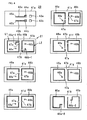
- a wireless IC device of a first embodiment includes a wireless IC chip 10 processing transmission and reception signals having predetermined frequencies and a feeder circuit board 20 on which the wireless IC chip 10 is mounted, which are shown in Fig. 3 .
- the wireless IC device of the first embodiment also includes a radiation substrate 30 shown in Fig. 2(A) or Fig. 2(B) .
- the feeder circuit board 20 includes a feeder circuit 21 (described in detail below with reference to Fig. 4 ) that includes a resonant circuit and/or a matching circuit including inductance elements L1 and L2.
- the inductance of the inductance element L1 is different from that of the inductance element L2 and the inductance element L1 is out of phase with and magnetically coupled to the inductance element L2 (indicated by a mutual inductance M).
- the wireless IC chip 10 includes a clock circuit, a logic circuit, a memory circuit, and so on. Necessary information is stored in the wireless IC chip 10.
- a pair of input-output terminal electrodes and a pair of mounting terminal electrodes, which are not shown in the drawings, are provided on the rear face of the wireless IC chip 10. As shown in Fig. 3 , the input-output terminal electrodes are electrically connected to feeder terminal electrodes 42a and 42b formed on the feeder circuit board 20 via metal bumps or the likes, and the mounting terminal electrodes are electrically connected to mounting electrodes 43a and 43b formed on the feeder circuit board 20 via metal bumps or the likes.
- a loop radiation strip 32 made of a nonmagnetic metal material is formed along the periphery on a flexible resin film base 31.
- the feeder circuit board 20 is adhered to one end 32a of the radiation strip 32 and the other end 32b thereof via adhesive.
- the ends 32a and 32b are each coupled to either of the inductance elements L1 and L2 in the feeder circuit 21.
- a magnetic body 33 is arranged inside the loop of the radiation strip 32.
- Fig. 2(B) shows a state where the feeder circuit board 20 on which the wireless IC chip 10 is mounted is adhered on the radiation strip 32 on the radiation substrate 30.
- the inductance elements L1 and L2 included in the feeder circuit 21 are out of phase with and magnetically coupled to each other to resonate with the frequency processed by the wireless IC chip 10 and to be electromagnetically coupled to the ends 32a and 32b of the radiation strip 32.
- the feeder circuit 21 matches the impedance (normally 50 ⁇ ) of the wireless IC chip 10 with the impedance (a spatial impedance of 377 ⁇ ) of the radiation strip 32.
- the feeder circuit 21 supplies a transmission signal that is sent from the wireless IC chip 10 and that has a predetermined frequency to the radiation strip 32 and selects a reception signal having a predetermined frequency from the signals received by the radiation strip 32 to supply the selected signal to the wireless IC chip 10.
- the wireless IC chip 10 operates in response to the signal received by the radiation strip 32 and a response signal from the wireless IC chip 10 is externally radiated from the radiation strip 32.
- the wireless IC device since the resonant frequency of a signal is set in the feeder circuit 21 provided on the feeder circuit board 20 in the wireless IC device, the wireless IC device normally operates even if the wireless IC device is mounted on various articles and a variation in the radiation characteristics is suppressed, thus eliminating the need for changing the design of the radiation strip 32, etc. for every article.
- the frequency of a transmission signal radiated from the radiation strip 32 and the frequency of a reception signal supplied to the wireless IC chip 10 substantially correspond to the resonant frequency of the feeder circuit 21 on the feeder circuit board 20.
- the maximum gain of a signal is substantially determined by at least one of the size and shape of the feeder circuit 21 and the distance and the medium between the feeder circuit and the radiation strip.
- the frequency characteristics are not varied even if, for example, the wireless IC device is rolled or is sandwiched between dielectric materials, thus achieving the stable frequency characteristics regardless of the shape, size, and arrangement of the radiation strip 32.
- the feeder circuit board 20 is manufactured by layering, attaching by pressure, and firing ceramic sheets 41a to 41h made of a dielectric material or a magnetic material.
- Feeder terminal electrodes 42a and 42b, mounting electrodes 43a and 43b, and via-hole conductors 44a, 44b, 45a, and 45b are formed on the top-layer sheet 41a.
- Wiring electrodes 46a and 46b composing the inductance elements L1 and L2, respectively, are formed on the respective layers from the second-layer sheet 41b to the eighth-layer sheet 41h.
- Via-hole conductors 47a, 47b, 48a, and 48b are formed on the layers from the second-layer sheet 41b to the eighth-layer sheet 41h, if needed.
- Layering the above sheets 41a to 41h forms the inductance element L1 in which the wiring electrodes 46a are helically connected to each other via the via-hole conductor 47a and forms the inductance element L2 in which the wiring electrodes 46b are helically connected to each other via the via-hole conductor 47b.
- a capacitance is generated between the lines of the wiring electrodes 46a and 46b.
- An end 46a-1 of the wiring electrode 46a on the sheet 41b is connected to the feeder terminal electrode 42a via the via-hole conductor 45a, and an end 46a-2 of the wiring electrode 46a on the sheet 41h is connected to the feeder terminal electrode 42b via the via-hole conductors 48a and 45b.
- An end 46b-1 of the wiring electrode 46b on the sheet 41b is connected to the feeder terminal electrode 42b via the via-hole conductor 44b, and an end 46b-2 of the wiring electrode 46b on the sheet 41h is connected to the feeder terminal electrode 42a via the via-hole conductors 48b and 44a.
- the inductance elements L1 and L2 are wound in opposite directions around the winding axes that are substantially parallel to each other in the above feeder circuit 21, the magnetic field generated in the inductance element L1 is offset by the magnetic field generated in the inductance element L2. It is necessary to increase the lengths of the wiring electrodes 46a and 46b to some extent in order to generate a desired inductance because the magnetic fields are offset by each other. This reduces the Q value to suppress the steepness of the resonance characteristics, thereby broaden the resonance characteristics near the resonant frequency.
- the inductance elements L1 and L2 are formed at different left-side and right-side positions.
- the direction of the magnetic field generated in the inductance element L1 is opposite to that of the magnetic field generated in the inductance element L2. Accordingly, when the feeder circuit 21 is coupled to the ends 32a and 32b of the loop radiation strip 32, a current excited at the end 32a flows in the direction opposite to the direction in which a current excited at the end 32b flows and, therefore, signals can be transmitted and received with the loop radiation strip 32.
- the inductance elements L1 and L2 may be coupled to different radiation strips.
- the radiation strip 32 is composed of a loop electrode having the one end 32a and the other end 32b, and the ends 32a and 32b are coupled to the different inductance elements L1 and L2, respectively.
- the magnetic body 33 made of, for example, ferrite is arranged inside the loop of the loop electrode. The presence of the magnetic body 33 causes amplification of the magnetic field generated around the radiation strip 32 composed of the loop electrode to increase the communication distance.
- the magnetic body 33 may not necessarily be provided and may be omitted.
- the feeder circuit board 20 is made of a magnetic material and the inductance elements L1 and L2 are formed in the magnetic body, a higher inductance is generated and the frequencies around 13.56 MHz are supported.
- the magnetic material preferably has a permittivity ⁇ of around 400.
- the feeder circuit board 20 may be a multilayer board made of ceramics or resin or may be a board in which flexible sheets made of a dielectric material, such as polyimide or liquid crystal polymer, are layered. Particularly, incorporating the inductance elements L1 and L2 in the feeder circuit board 20 causes the feeder circuit 21 to be less susceptible to the outside of the board, thereby suppressing a variation in the radiation characteristics.
- the feeder circuit board 20 may not be adhered on the ends 32a and 32b of the radiation strip 32.
- the feeder circuit board 20 may be arranged in proximity to the ends 32a and 32b.
- a wireless IC device of a second embodiment basically has a structure similar to that of the first embodiment. As shown in Fig. 5 , the wireless IC device of the second embodiment differs from the first embodiment in that, in a perspective plan view of the feeder circuit board 20, planer electrodes 49a and 49b are provided on the rear face of a sheet 41i that is the bottom layer of the feeder circuit board 20.
- the planer electrodes 49a and 49b have the same outer dimensions as those of the inductance elements L1 and L2 or have outer dimensions smaller than those of the inductance elements L1 and L2.
- Via-hole conductors are arranged at the respective ends 46a-2 and 46b-2 of the wiring electrodes 46a and 46b forming the inductance elements L1 and L2.
- the via-hole conductors are connected to the feeder terminal electrodes 42a and 42b and are also connected to the planer electrodes 49a and 49b via via-hole conductors 48c and 48d formed in the sheet 41i.
- the provision of the planer electrodes 49a and 49b allows a variation in coupling between the feeder circuit 21 and the radiation strip 32 to be suppressed.
- the planer electrodes 49a and 49b may not be electrically connected to the wiring electrodes 46a and 46b.
- the planer electrodes 49a and 49b may be electrically connected to the radiation strip 32.
- the feeder circuit board 20 on which the wireless.IC chip 10 is mounted is adhered on an end 53b of an electrode 53 and an electrode 54, which are formed on the front face of a radiation substrate 50, with adhesive.
- the wireless IC chip 10 of the third embodiment has the same structure as that of the first embodiment.
- the radiation substrate 50 has the spiral electrode 53 and the electrode 54 that are formed on the front face of a flexible resin film base 51 and that function as a radiation strip 52.
- the radiation substrate 50 has a spiral electrode 55 that is provided on the rear face of the flexible resin film base 51 and that functions as the radiation strip 52.
- An end 53a of the electrode 53 is electrically connected to an end 55a of the electrode 55 via a via-hole conductor 56a and an end 55b of the electrode 55 is electrically connected to the electrode 54 via a via-hole conductor 56b.
- a magnetic body 57 made of, for example, ferrite is formed on the rear face of the substrate 50.
- the magnetic body 57 is formed on the electrode 55 inside the outline of the electrode 55.
- the magnetic body 57 may be made of a magnetic metal material. In this case, it is necessary to electrically insulate the magnetic body 57 from the electrode 55.
- inductance elements L1 and L2 having different inductances are magnetically coupled to each other in phase (a mutual inductance M1), and inductance elements L3 and L4 having different inductances are magnetically coupled to each other in phase (the mutual inductance M1).
- the inductance elements L1 and L2 are out of phase with and magnetically coupled to the inductance elements L3 and L4 (indicated by a mutual inductance M2).
- the feeder circuit 21 including a resonant circuit and/or a matching circuit that include the inductance elements L1, L2, L3, and L4 will be described below with reference to Fig. 8 .
- the inductance elements L1 and L2 included in the feeder circuit 21 are out of phase with and magnetically coupled to the inductance elements L3 and L4 included in the feeder circuit 21 to resonate with the frequency processed by the wireless IC chip 10 and to be electromagnetically coupled to the electrode end 53b and the electrode 54 of the loop radiation strip 52.
- Feeder terminal electrode 62a and 62b in the feeder circuit 21 are electrically connected to input-output terminal electrodes (not shown) of the wireless IC chip 10 to match the impedance (normally 50 ⁇ ) of the wireless IC chip 10 with the impedance (a spatial impedance of 377 ⁇ ) of the radiation strip 52.
- a signal of a positive polarity is applied to the electrode 54 of the radiation strip 52
- a signal of a negative polarity is applied to the electrode end 53b.
- a current flows in the direction from the positive polarity (the electrode 54) to the negative polarity (the electrode end 53b) to transmit the signal between the radiation strip 52 and the feeder circuit 21.
- the feeder circuit 21 transmits a transmission signal that is sent from the wireless IC chip 10 and that has a predetermined frequency to the radiation strip 52 and selects a reception signal having a predetermined frequency from the signals received by the radiation strip 52 to supply the selected reception signal to the wireless IC chip 10, as in the first embodiment. Consequently, in the wireless IC device, the wireless IC chip 10 operates in response to the signal received by the radiation strip 52 and a response signal from the wireless IC chip 10 is externally radiated from the radiation strip 52. As described above, the operation and effect of the third embodiment are basically the same as those of the
- the feeder circuit board 20 is manufactured by layering, attaching by pressure, and firing ceramic sheets 61a to 61h made of a dielectric material or a magnetic material.
- the feeder terminal electrodes 62a and 62b, mounting electrodes 63a and 63b, and via-hole conductors 64a, 64b, 65a, and 65b are formed on the top-layer sheet 61a.
- Wiring electrodes 66a, 66b, 66c, and 66d composing the inductance elements L1, L2, L3, and L4 are formed on the layers from the second-layer sheet 61b to the eighth-layer sheet 61h.
- Via-hole conductors 67a, 67b, 68a, and 68b are formed on the layers from the second-layer sheet 61b to the eighth-layer sheet 61h, if needed.
- the inductance element L1 in which the wiring electrodes 66a are helically connected to each other via the via-hole conductor 67a and forms the inductance element L2 in which the wiring electrodes 66b are helically connected to each other via the via-hole conductor 67b.
- An end 66-1 where the wiring electrode 66a is integrated with the wiring electrode 66b on the sheet 61b is connected to the feeder terminal electrode 62a via the via-hole conductors 65a, and an end 66-2 where the wiring electrode 66a is integrated with the wiring electrode 66b on the sheet 41h is connected to the feeder terminal electrode 62b via the via-hole conductors 68a and 65b.
- An end 66-3 where the wiring electrode 66c is integrated with the wiring electrode 66d on the sheet 61b is connected to the feeder terminal electrode 62b via the via-hole conductors 64b, and 66-4 where the wiring electrode 66c is integrated with the wiring electrode 66d on the sheet 61h is connected to the feeder terminal electrode 62a via the via-hole conductors 68b and 64a.
- the operation of the feeder circuit 21 having the above structure is basically the same as that of the feeder circuit 21 described above in the first embodiment.
- the inductance elements L1 and L2 are formed of the two wiring electrodes 66a and 66b, which are adjacent to each other on the same plane
- the inductance elements L3 and L4 are formed of the wiring electrodes 66c and 66d, which are adjacent to each other on the same plane
- the lengths of the wiring electrodes or the distance between the electrodes can be varied to broaden the resonance characteristics.
- the radiation strip 52 is composed of a loop electrode having one end electrode 53a and the other end electrode 54, and the end electrodes 53a and 54 are coupled to the inductance elements L1 and L2 and the inductance elements L3 and L4, respectively. Since the magnetic body 57 is arranged inside the outline of the loop of the loop electrode, the magnetic field generated around the radiation strip 52 composed of the loop electrode is amplified to increase the communication distance.
- the magnetic body 57 may not necessarily be provided and may be omitted.
- a wireless IC device of a fourth embodiment includes the wireless IC chip 10, the feeder circuit board 20, and a radiation substrate 130 on which a radiation strip 132 is formed, as shown in Fig. 9 .
- the wireless IC chip 10 of the fourth embodiment has the same structure as that of the first embodiment.
- the feeder circuit board 20 includes the two inductance elements L1 and L2.
- Feeder terminal electrodes 72a and 72b and mounting electrodes 73a and 73b provided on the front face of the feeder circuit board 20 are electrically connected to input-output terminal electrodes and mounting terminal electrodes (which are not shown) below the wireless IC chip 10.
- the radiation strip 132 is helically formed on a half area of the front face of a base 131 made of ceramics and an auxiliary electrode 133 is helically formed on the other half area.
- the feeder circuit board 20 on which the wireless IC chip 10 is mounted is adhered on the radiation strip 132 with adhesive.
- an end 133a at the central portion of the auxiliary electrode 133 is connected to an electrode 135 formed on the rear face of the base 131 via a via-hole conductor 134, and an end 135a of the electrode 135 is capacitively coupled to an end 132a at the central portion of the radiation strip 132.
- the electrode 135 may be formed inside the base 131.
- the feeder circuit board 20 is manufactured by layering, attaching by pressure, and firing ceramic sheets 71a to 71e made of a dielectric material or a magnetic material, as shown in Fig. 10 .
- the feeder terminal electrodes 72a and 72b, the mounting electrodes 73a and 73b, and via-hole conductors 74a and 74b are formed on the top-layer sheet 71a.
- Wiring electrodes 75a and 75b composing the inductance elements L1 and L2, respectively, and via-hole conductors 76a, 76b, and 77 are formed on the layers from the second-layer sheet 71b to the fourth-layer sheet 71d.
- a wiring electrode 75 is formed on the bottom-layer sheet 71e.
- the wiring electrodes 75a and 75 are formed in a state where the wiring electrodes 75a and 75 are bare along the periphery of the sheets 71b to 71e.
- Layering the above sheets 71a to 71e forms the inductance element L1 in which the wiring electrodes 75a are helically connected to each other via the via-hole conductor 76a and forms the inductance element L2 in which the wiring electrodes 75b are helically connected to each other via the via-hole conductor 76b.
- the wiring electrodes 75a and 75b branch off on the sheet 71b and the wiring electrodes 75a and 75b are integrated into the wiring electrode 75 on the bottom-layer sheet 71e.
- a capacitance is generated between the lines of the wiring electrodes 75a and 75b.
- An end 75c where the wiring electrode 75a is integrated with the wiring electrode 75b on the sheet 71b is connected to the feeder terminal electrode 72b via the via-hole conductor 74b, an end 75d of the wiring electrode 75 on the sheet 71e is connected to the wiring electrodes 75a and 75b via the via-hole conductors 76a and 76b on the sheet 71d above the sheet 71e, and an end 75e of the wiring electrode 75 is connected to the feeder terminal electrode 72a via the via-hole conductors 77 and 74a.
- the feeder circuit 21 which has the above structure and which includes the inductance elements L1 and L2, has an equivalent circuit similar to that of the feeder circuit 21 shown in Fig. 1 .
- the inductance element L1 is out of phase with and electromagnetically coupled to the inductance element L2 to resonate with the frequency processed by the wireless IC chip 10 and to be electromagnetically coupled to the radiation strip 132.
- the feeder circuit 21 matches the impedance (normally 50 ⁇ ) of the wireless IC chip 10 with the impedance (a spatial impedance of 377 ⁇ ) of the radiation strip 132.
- the operation and effect of the fourth embodiment are the same as those of the first embodiment.
- part (the wiring electrodes 75a and 75) of the inductance elements L1 and L2 is bare along the side faces of the feeder circuit board 20 in the fourth embodiment, the part that is exposed to the outside also functions as the radiation strip.
- the part of the inductance elements L1 and L2 exposed to the outside is electromagnetically coupled to the radiation strip 132 and the auxiliary electrode 133 on the side faces of the feeder circuit board 20, so that the radiation characteristics are improved.
- the external dimension of the auxiliary electrode 133 is the same as or greater than that of the feeder circuit board 20 and, thus, the coupling to the magnetic field radiated from the rear face and the side faces of the feeder circuit board 20 is easily achieved.
- a wireless IC device of a fifth embodiment includes the feeder circuit board 20 shown in Fig. 11 .
- the wireless IC chip 10 and the radiation substrate 30, which are the remaining components of the wireless IC device, are the same as those described in the first embodiment.
- the feeder circuit board 20 is manufactured by layering, attaching by pressure, and firing ceramic sheets 81a to 81e made of a dielectric material or a magnetic material.
- Feeder terminal electrodes 82a and 82b, mounting electrodes 83a and 83b, and via-hole conductors 84a and 84b are formed on the top-layer sheet 81a.
- a wiring electrode 85 and via-hole conductors 86a, 86b, 87a, and 87b are formed on the second-layer sheet 81b.
- Wiring electrodes 85a and 85b composing the inductance elements L1 and L2 and the via-hole conductors 86a, 86b, 87a, and 87b are formed on the third-layer sheet 81c.
- the wiring electrodes 85a and 85b composing the inductance elements L1 and L2 are formed on the fourth-layer sheet 81d.
- Planer electrodes 88a and 88b are formed on rear face of the bottom-layer sheet 81e
- Layering the above sheets 81a to 81e forms the inductance element L1 in which the wiring electrodes 85a are helically connected to each other via the via-hole conductor 86a and forms the inductance element L2 in which the wiring electrodes 85b are helically connected to each other via the via-hole conductor 86b.
- a capacitance is generated between the lines of the wiring electrodes 85a and 85b.
- the wiring electrodes 85a and 85b are integrated into the wiring electrode 85 on the sheet 81b, an end 85a' of the wiring electrode 85a on the sheet 81d is connected to the feeder terminal electrode 82a via the via-hole conductors 87a and 84a, and an end 85b' of the wiring electrode 85b on the sheet 81d is connected to the feeder terminal electrode 82b via the via-hole conductors 87b and 84b.
- the feeder circuit 21, which has the above structure' and which includes the inductance elements L1 and L2, has an equivalent circuit similar to that of the feeder circuit 21 shown in Fig. 1 .
- the inductance element L1 is out of phase with and electromagnetically coupled to the inductance element L2 to resonate with the frequency processed by the wireless IC chip 10 and to be electromagnetically coupled to the radiation strip 32.
- the feeder circuit 21 matches the impedance (normally 50 ⁇ ) of the wireless IC chip 10 with the impedance (a spatial impedance of 377 ⁇ ) of the radiation strip 32.
- the operation and effect of the fifth embodiment are the same as those of the first embodiment.
- the provision of the planer electrodes 88a and 88b on the rear face of the feeder circuit board 20 allows a variation in coupling between the feeder circuit 21 and the radiation strip 32 to be suppressed.
- the planer electrodes 88a and 88b may not necessarily be provided.
- a wireless IC device of a sixth embodiment includes the feeder circuit board 20 shown in Fig. 12 .
- the wireless IC chip 10 and the radiation substrate 30, which are the remaining components of the wireless IC device, are the same as those described in the first embodiment.
- the structure of the feeder circuit board 20 is basically the same as that of the feeder circuit board 20 shown in the first embodiment.
- Wiring electrodes 101a and 101b helically connected to each other form the inductance elements L1 and L2, respectively.
- the inductance elements L1 and L2 have different inductances and are out of phase with and magnetically coupled to each other.
- Planer electrodes 102a and 102b are arranged beneath the inductance elements L1 and L2, and wiring electrodes 103 helically connected to each other form a magnetic-field receiving coil 104.
- the magnetic-field receiving coil 104 is connected in series to the planer electrodes 102a and 102b and has an auxiliary radiation function for coupling the feeder circuit 21 to the radiation strip 32 (refer to Fig. 2 ).
- the feeder circuit 21 of the sixth embodiment which includes the inductance elements L1 and L2, has an equivalent circuit similar to that of the feeder circuit 21 shown in Fig. 1 .
- the inductance element L1 is out of phase with and electromagnetically coupled to the inductance element L2 to resonate with the frequency processed by the wireless IC chip 10 and to be electromagnetically coupled to the radiation strip 32.
- the feeder circuit 21 matches the impedance (normally 50 ⁇ ) of the wireless IC chip 10 with the impedance (a spatial impedance of 377 ⁇ ) of the radiation strip 32. Accordingly, the operation and effect of the sixth embodiment are similar to those of the first embodiment.
- a wireless IC device of a seventh embodiment includes the feeder circuit board 20 shown in Fig. 13 .
- the wireless IC chip 10 and the radiation substrate 30, which are the remaining components of the wireless IC device, are the same as those described in the first embodiment.
- wiring electrodes 111a and 111b that are adjacent to each other and that are helically connected to each other form the inductance elements L1 and L2, respectively.
- the inductance elements L1 and L2 have different inductances and are out of phase with and magnetically coupled to each other.
- Planer electrodes 112a and 112b are arranged beneath the inductance elements L1 and L2, and wiring electrodes 113 that are helically connected to each other form a magnetic-field receiving coil 114.
- the magnetic-field receiving coil 114 is connected in series to the planer electrodes 112a and 112b and has an auxiliary radiation function for coupling the feeder circuit 21 to the radiation strip 32 (refer to Fig. 2 ) .
- the feeder circuit 21 of the seventh embodiment which includes the inductance elements L1 and L2, has an equivalent circuit similar to that of the feeder circuit 21 shown in Fig. 1 .
- the inductance element L1 is out of phase with and electromagnetically coupled to the inductance element L2 to resonate with the frequency processed by the wireless IC chip 10 and to be electromagnetically coupled to the radiation strip 32.
- the feeder circuit 21 matches the impedance (normally 50 ⁇ ) of the wireless IC chip 10 with the impedance (a spatial impedance of 377 ⁇ ) of the radiation strip 32. Accordingly, the operation and effect of the seventh embodiment are similar to those of the first embodiment.
- the inductance elements L1 and L2 are composed of the two wiring electrodes 111a and 111b that are adjacent to each other on the same plane, respectively, the lengths of the wiring electrodes 111a and 111b or the distance between the wiring electrodes 111a and 11b can be varied to broaden the resonance characteristics.
- a wireless IC device of an eighth embodiment includes the feeder circuit board 20 shown in Fig. 14 .
- the feeder circuit 21 on the feeder circuit board 20 is basically the same as in the fifth embodiment (refer to Fig. 11 ). Specifically, feeder terminal electrodes 122a and 122b and mounting electrode 123a and 123b are formed on a sheet 121a, and wiring electrodes 125a and 125b are formed on sheets 121b to 121g. Planer electrodes 128a and 128b are formed on a sheet 121h.
- the inductance elements L1 and L2 are formed by helically connecting the wiring electrodes 125a and 125b, respectively, and the wiring electrodes 125a and 125b are integrated into a wiring electrode 125 on the sheet 121b.
- An end 125a' of the wiring electrode 125a on the sheet 121g is connected to the feeder terminal electrode 122a and an end 125b' of the wiring electrode 125b on the sheet 121g is connected to the feeder terminal electrode 122b.
- the feeder circuit 21 which has the above structure and which includes the inductance elements L1 and L2, has an equivalent circuit shown in Fig. 15 .
- the inductance elements L1 and L2 connected in series to the wireless IC chip 10 are out of phase with and electromagnetically coupled to each other to resonate with the frequency processed by the wireless IC chip 10 and to be electromagnetically coupled to the radiation strip 52 (may be the radiation strip 32).
- the feeder circuit 21 matches the impedance (normally 50 ⁇ ) of the wireless IC chip 10 with the impedance (a spatial impedance of 377 ⁇ ) of the radiation strip 32, 52.
- the operation and effect of the eighth embodiment are similar to those of the first embodiment.
- the provision of the planer electrodes 128a and 128b on the rear face of the feeder circuit board 20 allows a variation in coupling between the feeder circuit 21 and the radiation strip 32, 52 to be suppressed.
- the planer electrodes 128a and 128b may not necessarily be provided.
- the positions where the ends of the inductance elements L1 and L2 are connected to the feeder terminal electrodes 122a and 122b can be varied and the ends 125a' and 125b' can be electrically opened to compose an auxiliary matching circuit.
- extending electrodes 125a" and 125b" are formed for the wiring electrodes 125a and 125b on the sheet 121e and the extending electrodes 125a" and 125b" are connected to the feeder terminal electrodes 122a and 122b, respectively.
- the ends 125a' and 125b' of the wiring electrodes 125a and 125b on the sheet 121g are electrically opened to form an auxiliary matching circuit 129 by using the wiring electrodes 125a and 125b on the sheets 121f and 121g.
- the extending electrodes 125a" and 125b" connected to the feeder terminal electrodes 122a and 122b, respectively, may be any of the wiring electrodes 125a and 125b provided on the sheets 121c to 121f.
- An equivalent circuit including the extending electrodes 125a" and 125b" is shown in Fig. 17 .
- the formation of the auxiliary matching circuit 129 enables fine adjustment of the matching state.
- the feeder circuit board 20 provided with the wireless IC chip 10 is adhered on the radiation substrate 30, as shown in Fig. 18 , and the radiation substrate 30 is adhered to a depression 141 on the front face or the rear face of a metal can 140, as shown in Fig. 19 .
- the metal can 140 is made of a metallic material, such as steel or aluminum.
- the feeder circuit board 20 is the same as the one shown in the first embodiment and has the feeder circuit 21 shown in Fig. 4 .
- the radiation substrate 30 has the loop radiation strip 32 shown in Fig. 2 formed thereon.
- the radiation strip 32 is provided on the film base 31 and has the ends 32a and 32b.
- the film base 31 and the radiation strip 32 shown in Fig. 2 have quadrangular shapes whereas the film base 31 and the radiation strip 32 of the ninth embodiment have elliptical shapes, as shown in Fig. 18 .
- the radiation substrate 30 provided with the wireless IC chip 10 and the feeder circuit board 20 is adhered on the bottom of the depression 141 via a mount 142 having adhesive on both sides.
- a depth H1 of the depression 141 is about five mm and a distance H2 from the bottom of the depression 141 to the radiation strip 32 is around two to three mm.
- the wireless IC chip 10 does not preferably protrude from the depression 141.
- the operation and effect of the ninth embodiment are similar to those of the first embodiment.
- magnetic fields ⁇ (refer to Fig. 20 ) are generated around the loop radiation strip 32. Since the magnetic fields do not pass through a metal, arranging a metal in parallel with and close to the radiation strip 32 causes the magnetic fields generated around the radiation strip 32 to be blocked by the metal. In such a case, the magnetic fields are not sufficiently radiated externally to cause the insufficient operation of the wireless IC device.
- arranging the radiation strip 32 away from the bottom of the depression 141 of the radiation strip metal can 140 by about a few millimeters via, for example, the mount 142 allows the magnetic fields ⁇ to be radiated from the radiation strip 32 to ensure the operation of the wireless IC device.
- the radiation substrate 30 provided with the feeder circuit board 20 may be embedded in the mount 142.
- the radiation substrate 30 may have a thickness similar to that of the mount 142 and the feeder circuit board 20 may be embedded in a depression formed in the radiation substrate 30.
- the wireless IC chip 10 may be arranged so as to be sandwiched between the feeder circuit board 20 and the radiation substrate 30. With the above structures, it is possible to protect the wireless IC chip and the feeder circuit board 20 from dropping or impact to improve the mechanical strength of the wireless IC device.
- the wireless IC device is adhered to the metal can 140 in the ninth embodiment, the object to which the wireless IC device is adhered is not restricted to the metal can.
- the wireless IC device may be adhered to any metallic article, such as a metallic case or a ground electrode on the circuit board.
- the feeder circuit boards each include the feeder circuit board provided with the feeder circuit including a resonant circuit and/or a matching circuit in the above embodiments.
- a feeder circuit including a resonant circuit and/or a matching circuit that include at least two inductance elements may be provided on the rear face (the main face) of the wireless IC chip where the input-output terminal electrodes are formed, without providing the feeder circuit board.
- Such wireless IC devices will be described as a tenth embodiment and an eleventh embodiment.
- a feeder circuit 150 shown in Fig. 21 as an equivalent circuit is provided on the rear face of the wireless IC chip 10.
- the feeder circuit 150 is composed of the two helically-formed inductance elements L1 and L2 that are wound in opposite directions and that are connected in series to each other.
- Feeder terminal electrodes 151a and 151b provided at ends of the respective inductance elements L1 and L2 are electrically conducted to an input terminal electrode and an output terminal electrode of the wireless IC chip 10.
- the inductance elements L1 and L2 are out of phase with and electromagnetically coupled to each other, a resonant circuit composed of the inductance elements L1 and L2 and a stray capacitance between the lines resonates with the frequency processed by the wireless IC chip 10, and the inductance elements L1 and L2 are electromagnetically coupled to a radiation strip (for example, the ends 32a and 32b of the radiation strip 32 shown in Fig. 2 ). Accordingly, the operation and effect of the tenth embodiment is similar to those of the first embodiment.
- a midpoint between the inductance elements L1 and L2 serves as a virtual ground.
- the impedance of the feeder circuit 150 is designed so as to make a complex conjugate with the impedance of the wireless IC chip 10. Since the inductance elements L1 and L2 are formed in a layered state shown in Fig. 22 , the inductance elements L1 and L2 have different inductances depending on the distance to the radiation strip. Accordingly, an insulating layer 159 is formed on the rear face of the wireless IC chip 10 to fix the distance from the radiation strip and to protect the inductance elements L1 and L2.
- the feeder circuit 150 is manufactured through processes shown in Fig. 22 .
- an insulating layer 154 is formed on the electrode layer 153.
- an electrode layer 155 is formed on the insulating layer 154 by plating or the like and the electrode layer 155 is etched into a certain shape (refer to Fig. 22(f) ). This state is shown in Fig. 23(B) .
- the insulating layer 159 is formed on the electrode layer 155.
- the feeder circuit 150 shown in Fig. 24 as an equivalent circuit is provided on the rear face of the wireless IC chip 10.
- a capacitor C is provided between the inductance elements L1 and L2 in the equivalent circuit (refer to Fig. 21 ) shown in the ninth embodiment to form a serial resonant circuit.
- the operation and effect of the eleventh embodiment are similar to those of the first embodiment.
- the feeder circuit 150 shown in Fig. 24 is manufactured through processes shown in Fig. 25 .
- the insulating layer 152 is formed on the electrode layer 157.
- the electrode layer 153 is formed on the insulating layer 152 by plating or the like and the electrode layer 153 is etched into a certain shape (refer to Fig. 25(f) ). This state is shown in Fig. 26(B) . Electrodes 153a and 153b opposing the capacitor electrode 157a are formed at this stage.
- the insulating layer 154 is formed on the electrode layer 153. Subsequently, the electrode layer 155 and the insulating layer 159 are formed in the manner shown in Figs. 22(e), (f), and (g) . The state after the electrode layer 155 is formed is shown in Fig. 26(C) .
- a wireless IC device of a twelfth embodiment includes a feeder circuit 200 in which the helically-formed inductance elements L1 and L2 wound in opposite directions are connected in series to each other, as shown in an equivalent circuit in Fig. 27(A) .
- Both ends of a radiation strip 212 composed of a loop electrode including an inductance component L10 are electrically conducted to both ends of the inductance elements L1 and L2.
- Feeder terminal electrodes 201a and 201b connected to the input terminal electrode and the output terminal electrode of the wireless IC chip 10 are formed at both ends of the feeder circuit 200.
- a capacitor C is provided in parallel with the inductance elements L1 and L2.
- the remaining structure is similar to the structure of the twelfth embodiment.
- a wireless IC device of a fourteenth embodiment includes the feeder circuit 200 in which the helically-formed inductance elements L1 and L2 wound in opposite directions are connected in series to each other, as shown in an equivalent circuit in Fig. 28(A) .
- Helical inductance components L11 and L12 provided at both ends of the radiation strip 212 composed of the loop electrode including the inductance component L10 are electromagnetically coupled to the inductance elements L1 and L2, respectively.
- the feeder terminal electrodes 201a and 201b connected to the input terminal electrode and the output terminal electrode of the wireless IC chip 10 are formed at both ends of the feeder circuit 200.
- a wireless IC device of a fifteenth embodiment as shown in an equivalent circuit in Fig. 28(B) , the capacitor C is provided in parallel with the inductance elements L1 and L2.
- the remaining structure is similar to the structure of the fourteenth embodiment.
- the helical receiving electrodes are provided at both ends of the radiation strip 212 so as to oppose the inductance elements L1 and L2 in the feeder circuit 200. This allows the direction of the magnetic field generated around the inductance component L10 of the radiation strip 212 to be the same as the direction of the magnetic field generated in the feeder circuit 200, thus improving the degree of coupling between the feeder circuit 200 and the radiation strip 212.
- the inductance elements and the helical ends of the radiation strip 212 (L1 and L11 and L2 and L12), which are formed so as to be coupled to each other, are formed so as to be wound in the same direction in a perspective plan view of the feeder circuit 200.
- the magnetic fields of the same direction are generated in the respective two helical electrodes (L1 and L11 and L2 and L12) arranged so as to be opposed to each other in the perspective plan view, thus further increasing the degree of the magnetic-field coupling between the feeder circuit 200 and the radiation strip 212.
- the inductance (L10) of the loop electrode of the radiation strip 212 is set to a value higher than the inductances of the inductance elements L1 and L2 in the feeder circuit 200. Since signals generated in the feeder circuit 200 can be transmitted and received with the magnetic field generated around the radiation strip 212, it is possible to suppress an occurrence of communication failure with a reader-writer.
- these wireless IC devices each include the wireless IC chip 10, a feeder circuit board 220, and a radiation substrate 210 provided with the radiation strip 212 (refer to Fig. 31 ).
- the feeder terminal electrodes 201a and 201b are formed on the front face of the feeder circuit board 220 (refer to Fig. 29(B) ) and planar electrodes 202a and 202b are provided on the rear face thereof (refer to Fig. 29(C) ).
- the planar electrodes 202a and 202b have the operation and effect described in the second embodiment (refer to Fig. 5 ).
- the planar electrodes 202a and 202b may be omitted.
- the feeder circuit 200 shown in Fig. 30 is formed inside the feeder circuit board 220.
- the feeder circuit board 220 is manufactured by layering, attaching by pressure, and firing ceramic sheets made of a dielectric material or a magnetic material.
- the feeder terminal electrodes 201a and 201b and mounting electrodes 201c and 201d are formed on a top-layer sheet 231a.
- Connection electrodes 203a and 203b are formed on a second-layer sheet 231b.
- Wiring electrodes 204a and 204b composing the inductance elements L1 and L2, respectively, are formed on the sheets from a third-layer sheet 231c to a seventh-layer sheet 231g.
- Layering the above sheets 231a to 231g forms the inductance element L1 in which the wiring electrodes 204a are helically connected to each other via a via-hole conductor 205a and forms the inductance element L2 in which the wiring electrodes 204b are helically connected to each other via a via-hole conductor 205b.
- One end of the inductance element L1 (the wiring electrode 204a) is conductively connected to one end of the inductance element L2 (the wiring electrode 204b) on the sheet 231c, and the other end of the inductance element L1 and the other end of the inductance element L2 are connected to the feeder terminal electrodes 201a and 201b, respectively, via the connection electrodes 203a and 203b and via-hole conductors 206a and 206b.
- the feeder circuit 200 having the above structure has the same operation and effect as those described in the first and second embodiments. Particularly, in the feeder circuit 200 shown in Fig. 30 , one end of the inductance element L1 is conductively connected to one end of the inductance element L2 near the top layer in the multilayer body, and the other end of the inductance element L1 and the other end of the inductance element L2 are connected to the wireless IC chip 10.
- the inductance element L1 is conductively connected to the inductance element L2 near the top layer in the multilayer body, which is away from the radiation strip 212, and the inductance elements L1 and L2 are wound in opposite directions near the bottom layer in the multilayer body, which is electromagnetically coupled to the radiation strip 212, so that the efficiency of energy transfer is improved.
- the radiation strip 212 having one end 212a and the other end 212b is helically formed on the front face of the flexible resin film base 211 and an electrode 213 adjacent to the end 212a is formed.
- the electrode 213 is electrically conducted to the other end 212b of the radiation strip 212 via a connection electrode 214 formed on the rear face of the base 211 and a via-hole conductor.
- the feeder circuit board 220 on which the wireless IC chip 10 is mounted is coupled to the end 212a of the radiation strip 212 and an end 213a of the electrode 213.
- the end 212a of the radiation strip 212 and the end 213a of the electrode 213 may have planer shapes, as shown in Fig. 31(B) , or may be helically formed, as shown in Fig. 31(C) .
- the case where the end 212a of the radiation strip 212 and the end 213a of the electrode 213 are helically formed corresponds to the fourteenth and fifteenth embodiments.
- the at least two inductance elements may be formed at different positions in a perspective plan view of the feeder circuit in the wireless IC devices described above.
- the feeder circuit can be coupled to two different radiation strips.
- the at least two inductance elements may be formed of two wiring electrodes adjacent to each other on the same plane. When one inductance element is composed of two adjacent wiring electrodes, the length of the wiring electrodes or the distance between the wiring electrodes can be varied to broaden the resonance characteristics.
- the feeder circuit board may be formed of a multilayer body, and the planer electrodes having outer dimensions that are the same as or smaller than those of the at least two inductance elements may be provided inside or on the front face of the bottom layer of the multilayer body in a perspective plan view of the feeder circuit board.
- the provision of the planer electrodes allows a variation in coupling between the feeder circuit and the radiation strip to be suppressed.
- the feeder circuit board may include a magnetic body and the at least two inductance elements may be formed inside the magnetic body.
- the inclusion of the magnetic body in the feeder circuit board achieves a higher inductance and allows frequencies around 13.56-MHz band to be supported.
- one end of a inductance element may be conductively connected to one end of the other inductance element near the top layer in the multilayer body and the other ends of the inductance elements may be coupled to the wireless IC.
- the two inductance elements are conductively connected to each other near the top layer in the multilayer body, which is away from the radiation strip, and are wound in opposite directions near the bottom layer in the multilayer body, which is electromagnetically coupled to the radiation strip, so that the efficiency of energy transfer is improved.
- the radiation strip may be composed of a loop electrode having one end and the other end.
- the one end and the other end may be coupled to the at least two different inductance elements and may be helically formed with being wound in opposite directions. Since the direction of the magnetic field generated at the side of the radiation strip can be the same direction as that of the magnetic field generated in the feeder circuit, the degree of coupling between the feeder circuit and the radiation strip is increased. It is preferred that the inductance element and the helical end of the radiation strip, which are formed so as to be coupled to each other, be formed so as to be wound in the same direction in a perspective plan view of the feeder circuit.
- the magnetic fields of the same direction are generated in the two helical electrodes arranged so as to be opposed to each other in the perspective plan view, so that the magnetic-field coupling between the feeder circuit and the radiation strip is further increased. Furthermore, it is preferred that the inductances of the loop electrodes be higher than those of the inductance elements in the feeder circuit. Since signals generated in the feeder circuit can be transmitted and received with the magnetic field generated around the radiation strip, it is possible to suppress an occurrence of communication failure with a reader-writer.
- the magnetic body may be arranged inside or on the front face of the loop of the loop electrode. In this case, the magnetic field generated around the radiation strip composed of the loop electrode is amplified, thus increasing the communication distance.
- the at least two inductance elements may be connected in series to the wireless IC, may be connected in parallel to the wireless IC, or may have substantially the same inductance.
- Multiple mounting electrodes for mounting the wireless IC may be formed on the main face of the feeder circuit board and the at least two mounting electrodes may be electrically conducted to each other via the feeder circuit.
- the at least two mounting electrodes may be balanced input-output terminal electrodes.
- the feeder circuit may include an auxiliary matching circuit in which one end may be electrically connected to a predetermined position in the feeder circuit and the other end is electrically opened.
- the auxiliary matching circuit enables fine adjustment of the matching state.
- the at least two mounting electrodes may be balanced input-output terminal electrodes.
- Part of the at least two inductance elements may be bare along the side faces of the feeder circuit board and the part that is exposed to the outside may be structured so as to also function as the radiation strip.
- the part of the inductance elements is electromagnetically coupled to the radiation strip on the side faces of the feeder circuit board to improve the radiation characteristics.
- the feeder circuit board may be a multilayer board made of ceramics or resin or may be a flexible board. Particularly, incorporating the inductance elements composing the feeder circuit in the board causes the feeder circuit to be less susceptible to the outside of the board, thereby suppressing a variation in the radiation characteristics.
- the at least two inductance elements may be conductively connected in series to each other. In this case, it is possible to reliably generate the magnetic fields of different directions in the inductance elements.
- the wireless IC device according to the present invention is not restricted to the above embodiments and various modifications may occur insofar as they are within the scope of the present invention.
- the wireless IC may not be of a chip type and may be integrated with the feeder circuit board.
- the radiation strip may adopt various shapes.
- the present invention is useful for a wireless IC device.
- the wireless IC device of the present invention is excellent in that the wireless IC device is less susceptible to, for example, the environment in which the wireless IC device is used, is capable of suppressing a variation in the radiation characteristics, and is capable of being used in a wideband.
Applications Claiming Priority (5)
| Application Number | Priority Date | Filing Date | Title |
|---|---|---|---|
| JP2007329360 | 2007-12-20 | ||
| JP2008177236 | 2008-07-07 | ||
| JP2008213164 | 2008-08-21 | ||
| PCT/JP2008/072260 WO2009081719A1 (ja) | 2007-12-20 | 2008-12-08 | 無線icデバイス |
| EP08865022A EP2096709B1 (de) | 2007-12-20 | 2008-12-08 | Ic-radiogerät |
Related Parent Applications (2)
| Application Number | Title | Priority Date | Filing Date |
|---|---|---|---|
| EP08865022.1 Division | 2008-12-08 | ||
| EP08865022A Division EP2096709B1 (de) | 2007-12-20 | 2008-12-08 | Ic-radiogerät |
Publications (2)
| Publication Number | Publication Date |
|---|---|
| EP2408064A1 true EP2408064A1 (de) | 2012-01-18 |
| EP2408064B1 EP2408064B1 (de) | 2020-08-05 |
Family
ID=40787963
Family Applications (2)
| Application Number | Title | Priority Date | Filing Date |
|---|---|---|---|
| EP08865022A Active EP2096709B1 (de) | 2007-12-20 | 2008-12-08 | Ic-radiogerät |
| EP11185009.5A Active EP2408064B1 (de) | 2007-12-20 | 2008-12-08 | Drahtlose integrierte Schaltung |
Family Applications Before (1)
| Application Number | Title | Priority Date | Filing Date |
|---|---|---|---|
| EP08865022A Active EP2096709B1 (de) | 2007-12-20 | 2008-12-08 | Ic-radiogerät |
Country Status (7)
| Country | Link |
|---|---|
| US (2) | US7990337B2 (de) |
| EP (2) | EP2096709B1 (de) |
| JP (2) | JP4462388B2 (de) |
| KR (2) | KR101047189B1 (de) |
| CN (1) | CN101595599B (de) |
| AT (1) | ATE555518T1 (de) |
| WO (1) | WO2009081719A1 (de) |
Families Citing this family (101)
| Publication number | Priority date | Publication date | Assignee | Title |
|---|---|---|---|---|
| US7519328B2 (en) | 2006-01-19 | 2009-04-14 | Murata Manufacturing Co., Ltd. | Wireless IC device and component for wireless IC device |
| US9064198B2 (en) | 2006-04-26 | 2015-06-23 | Murata Manufacturing Co., Ltd. | Electromagnetic-coupling-module-attached article |
| JP4281850B2 (ja) | 2006-06-30 | 2009-06-17 | 株式会社村田製作所 | 光ディスク |
| JP4775442B2 (ja) | 2006-09-26 | 2011-09-21 | 株式会社村田製作所 | 電磁結合モジュール付き物品 |
| US8235299B2 (en) | 2007-07-04 | 2012-08-07 | Murata Manufacturing Co., Ltd. | Wireless IC device and component for wireless IC device |
| WO2008136226A1 (ja) | 2007-04-26 | 2008-11-13 | Murata Manufacturing Co., Ltd. | 無線icデバイス |
| EP2148449B1 (de) | 2007-05-11 | 2012-12-12 | Murata Manufacturing Co., Ltd. | Drahtlose ic-vorrichtung |
| CN101542831B (zh) | 2007-07-09 | 2014-06-25 | 株式会社村田制作所 | 无线ic器件 |
| CN104540317B (zh) | 2007-07-17 | 2018-11-02 | 株式会社村田制作所 | 印制布线基板 |
| US20090021352A1 (en) | 2007-07-18 | 2009-01-22 | Murata Manufacturing Co., Ltd. | Radio frequency ic device and electronic apparatus |
| EP2086052B1 (de) * | 2007-07-18 | 2012-05-02 | Murata Manufacturing Co. Ltd. | Drahtloses ic-gerät |
| JP5104865B2 (ja) | 2007-07-18 | 2012-12-19 | 株式会社村田製作所 | 無線icデバイス |
| WO2009081719A1 (ja) | 2007-12-20 | 2009-07-02 | Murata Manufacturing Co., Ltd. | 無線icデバイス |
| CN101601169B (zh) | 2007-12-26 | 2013-08-14 | 株式会社村田制作所 | 天线装置及无线ic器件 |
| JP5267463B2 (ja) | 2008-03-03 | 2013-08-21 | 株式会社村田製作所 | 無線icデバイス及び無線通信システム |
| EP2284949B1 (de) | 2008-05-21 | 2016-08-03 | Murata Manufacturing Co. Ltd. | Drahtlose integrierte schaltung |
| WO2009142068A1 (ja) | 2008-05-22 | 2009-11-26 | 株式会社村田製作所 | 無線icデバイス及びその製造方法 |
| CN104077622B (zh) | 2008-05-26 | 2016-07-06 | 株式会社村田制作所 | 无线ic器件系统及无线ic器件的真伪判定方法 |
| JP4535210B2 (ja) | 2008-05-28 | 2010-09-01 | 株式会社村田製作所 | 無線icデバイス用部品および無線icデバイス |
| JP4557186B2 (ja) | 2008-06-25 | 2010-10-06 | 株式会社村田製作所 | 無線icデバイスとその製造方法 |
| WO2010001987A1 (ja) | 2008-07-04 | 2010-01-07 | 株式会社村田製作所 | 無線icデバイス |
| WO2010021217A1 (ja) | 2008-08-19 | 2010-02-25 | 株式会社村田製作所 | 無線icデバイス及びその製造方法 |
| JP5429182B2 (ja) | 2008-10-24 | 2014-02-26 | 株式会社村田製作所 | 無線icデバイス |
| DE112009002399B4 (de) | 2008-10-29 | 2022-08-18 | Murata Manufacturing Co., Ltd. | Funk-IC-Bauelement |
| DE112009002384B4 (de) * | 2008-11-17 | 2021-05-06 | Murata Manufacturing Co., Ltd. | Antenne und Drahtlose-IC-Bauelement |
| US8089418B2 (en) * | 2008-12-04 | 2012-01-03 | Intel Corporation | Antenna structure |
| CN103500873B (zh) | 2009-01-09 | 2016-08-31 | 株式会社村田制作所 | 无线ic器件及无线ic模块 |
| DE112009003613B4 (de) | 2009-01-16 | 2020-12-17 | Murata Manufacturing Co., Ltd. | Ic-bauelement |
| JP2010200309A (ja) * | 2009-01-30 | 2010-09-09 | Tdk Corp | 近接型アンテナ及び無線通信機 |
| EP2385580B1 (de) | 2009-01-30 | 2014-04-09 | Murata Manufacturing Co., Ltd. | Antenne und drahtlose ic-vorrichtung |
| EP2416355B1 (de) * | 2009-04-02 | 2016-12-21 | Murata Manufacturing Co., Ltd. | Schalttafel |
| JP5510450B2 (ja) | 2009-04-14 | 2014-06-04 | 株式会社村田製作所 | 無線icデバイス |
| JP4687832B2 (ja) * | 2009-04-21 | 2011-05-25 | 株式会社村田製作所 | アンテナ装置 |
| JP5532678B2 (ja) * | 2009-05-26 | 2014-06-25 | ソニー株式会社 | 通信装置、アンテナ装置、並びに通信システム |
| JP5447515B2 (ja) | 2009-06-03 | 2014-03-19 | 株式会社村田製作所 | 無線icデバイス及びその製造方法 |
| JP5516580B2 (ja) | 2009-06-19 | 2014-06-11 | 株式会社村田製作所 | 無線icデバイス及び給電回路と放射板との結合方法 |
| CN102474009B (zh) | 2009-07-03 | 2015-01-07 | 株式会社村田制作所 | 天线及天线模块 |
| JP5182431B2 (ja) | 2009-09-28 | 2013-04-17 | 株式会社村田製作所 | 無線icデバイスおよびそれを用いた環境状態検出方法 |
| CN102577646B (zh) | 2009-09-30 | 2015-03-04 | 株式会社村田制作所 | 电路基板及其制造方法 |
| JP5304580B2 (ja) | 2009-10-02 | 2013-10-02 | 株式会社村田製作所 | 無線icデバイス |
| WO2011045970A1 (ja) | 2009-10-16 | 2011-04-21 | 株式会社村田製作所 | アンテナ及び無線icデバイス |
| CN102598413A (zh) | 2009-10-27 | 2012-07-18 | 株式会社村田制作所 | 收发装置及无线标签读取装置 |
| JP5327334B2 (ja) | 2009-11-04 | 2013-10-30 | 株式会社村田製作所 | 通信端末及び情報処理システム |
| WO2011055702A1 (ja) * | 2009-11-04 | 2011-05-12 | 株式会社村田製作所 | 無線icタグ、リーダライタ及び情報処理システム |
| JP5333601B2 (ja) | 2009-11-04 | 2013-11-06 | 株式会社村田製作所 | 通信端末及び情報処理システム |
| CN102576929B (zh) | 2009-11-20 | 2015-01-28 | 株式会社村田制作所 | 天线装置以及移动通信终端 |
| WO2011077877A1 (ja) | 2009-12-24 | 2011-06-30 | 株式会社村田製作所 | アンテナ及び携帯端末 |
| JP4962629B2 (ja) * | 2010-01-19 | 2012-06-27 | 株式会社村田製作所 | 高周波トランス、電子回路および電子機器 |
| CN104953242B (zh) * | 2010-01-19 | 2019-03-26 | 株式会社村田制作所 | 天线装置及通信终端设备 |
| EP2388858B1 (de) | 2010-01-19 | 2016-09-21 | Murata Manufacturing Co., Ltd. | Antennenvorrichtung und kommunikationsendgerät |
| CN102763277A (zh) | 2010-02-19 | 2012-10-31 | 株式会社村田制作所 | 复合印刷布线基板及无线通信系统 |
| CN102782937B (zh) | 2010-03-03 | 2016-02-17 | 株式会社村田制作所 | 无线通信器件及无线通信终端 |
| JP5652470B2 (ja) | 2010-03-03 | 2015-01-14 | 株式会社村田製作所 | 無線通信モジュール及び無線通信デバイス |
| JP5477459B2 (ja) | 2010-03-12 | 2014-04-23 | 株式会社村田製作所 | 無線通信デバイス及び金属製物品 |
| JP5370581B2 (ja) | 2010-03-24 | 2013-12-18 | 株式会社村田製作所 | Rfidシステム |
| JP2011211309A (ja) * | 2010-03-29 | 2011-10-20 | Sony Corp | アンテナモジュール及び電子機器 |
| JP5630499B2 (ja) | 2010-03-31 | 2014-11-26 | 株式会社村田製作所 | アンテナ装置及び無線通信デバイス |
| WO2011122162A1 (ja) * | 2010-03-31 | 2011-10-06 | 株式会社村田製作所 | 複合アンテナ及び複合無線通信デバイス |
| CN102834970B (zh) * | 2010-04-26 | 2014-11-26 | 株式会社村田制作所 | 通信终端及卡式天线模块 |
| JP5170156B2 (ja) | 2010-05-14 | 2013-03-27 | 株式会社村田製作所 | 無線icデバイス |
| JP5299351B2 (ja) | 2010-05-14 | 2013-09-25 | 株式会社村田製作所 | 無線icデバイス |
| JP5376060B2 (ja) | 2010-07-08 | 2013-12-25 | 株式会社村田製作所 | アンテナ及びrfidデバイス |
| GB2495418B (en) | 2010-07-28 | 2017-05-24 | Murata Manufacturing Co | Antenna apparatus and communication terminal instrument |
| WO2012020748A1 (ja) | 2010-08-10 | 2012-02-16 | 株式会社村田製作所 | プリント配線板及び無線通信システム |
| EP2453581A4 (de) * | 2010-08-11 | 2014-04-09 | Murata Manufacturing Co | Frequenzstabilisierungsschaltung, antennenvorrichtung und kommunikationsendgerät |
| JP5234071B2 (ja) | 2010-09-03 | 2013-07-10 | 株式会社村田製作所 | Rficモジュール |
| JP2012064683A (ja) * | 2010-09-15 | 2012-03-29 | Murata Mfg Co Ltd | 積層型コイル |
| WO2012043432A1 (ja) | 2010-09-30 | 2012-04-05 | 株式会社村田製作所 | 無線icデバイス |
| CN105206919B (zh) | 2010-10-12 | 2018-11-02 | 株式会社村田制作所 | 天线装置及终端装置 |
| CN102971909B (zh) | 2010-10-21 | 2014-10-15 | 株式会社村田制作所 | 通信终端装置 |
| JP5234084B2 (ja) * | 2010-11-05 | 2013-07-10 | 株式会社村田製作所 | アンテナ装置および通信端末装置 |
| US10381720B2 (en) * | 2010-12-08 | 2019-08-13 | Nxp B.V. | Radio frequency identification (RFID) integrated circuit (IC) and matching network/antenna embedded in surface mount devices (SMD) |
| CN105048058B (zh) * | 2011-01-05 | 2017-10-27 | 株式会社村田制作所 | 无线通信器件 |
| CN103299325B (zh) | 2011-01-14 | 2016-03-02 | 株式会社村田制作所 | Rfid芯片封装以及rfid标签 |
| WO2012117843A1 (ja) | 2011-02-28 | 2012-09-07 | 株式会社村田製作所 | 無線通信デバイス |
| JP5630566B2 (ja) * | 2011-03-08 | 2014-11-26 | 株式会社村田製作所 | アンテナ装置及び通信端末機器 |
| EP2618424A4 (de) | 2011-04-05 | 2014-05-07 | Murata Manufacturing Co | Drahtlose kommunikationsvorrichtung |
| WO2012141070A1 (ja) | 2011-04-13 | 2012-10-18 | 株式会社村田製作所 | 無線icデバイス及び無線通信端末 |
| JP5569648B2 (ja) | 2011-05-16 | 2014-08-13 | 株式会社村田製作所 | 無線icデバイス |
| EP3041087B1 (de) | 2011-07-14 | 2022-09-07 | Murata Manufacturing Co., Ltd. | Drahtloskommunikationsvorrichtung |
| WO2013011856A1 (ja) | 2011-07-15 | 2013-01-24 | 株式会社村田製作所 | 無線通信デバイス |
| CN204189963U (zh) | 2011-07-19 | 2015-03-04 | 株式会社村田制作所 | 天线装置以及通信终端装置 |
| JP5709690B2 (ja) * | 2011-08-17 | 2015-04-30 | タイコエレクトロニクスジャパン合同会社 | アンテナ |
| WO2013035821A1 (ja) | 2011-09-09 | 2013-03-14 | 株式会社村田製作所 | アンテナ装置および無線デバイス |
| CN103380432B (zh) | 2011-12-01 | 2016-10-19 | 株式会社村田制作所 | 无线ic器件及其制造方法 |
| WO2013094667A1 (ja) * | 2011-12-22 | 2013-06-27 | 株式会社村田製作所 | 磁性体アンテナ、アンテナ装置及び電子機器 |
| CN103430382B (zh) * | 2012-01-30 | 2015-07-15 | 株式会社村田制作所 | 无线ic器件 |
| JP5464307B2 (ja) | 2012-02-24 | 2014-04-09 | 株式会社村田製作所 | アンテナ装置および無線通信装置 |
| CN104160554B (zh) * | 2012-03-30 | 2016-08-24 | 富士通株式会社 | Rfid标签 |
| JP5304975B1 (ja) | 2012-04-13 | 2013-10-02 | 株式会社村田製作所 | Rfidタグの検査方法及び検査装置 |
| CN204668075U (zh) * | 2013-02-19 | 2015-09-23 | 株式会社村田制作所 | 电感电桥及电子设备 |
| KR102010523B1 (ko) * | 2013-07-31 | 2019-08-13 | 삼성전자주식회사 | 안테나 장치 및 그것을 갖는 전자 장치 |
| CN206595403U (zh) * | 2014-01-30 | 2017-10-27 | 株式会社村田制作所 | 无线通信设备及无线通信用模块 |
| KR101762778B1 (ko) | 2014-03-04 | 2017-07-28 | 엘지이노텍 주식회사 | 무선 충전 및 통신 기판 그리고 무선 충전 및 통신 장치 |
| GB2539839B8 (en) * | 2014-04-28 | 2021-07-07 | Murata Manufacturing Co | Wireless IC device, clip-shaped RFID tag, and article having RFID tag |
| KR101892689B1 (ko) | 2014-10-14 | 2018-08-28 | 삼성전기주식회사 | 칩 전자부품 및 칩 전자부품의 실장 기판 |
| US9839134B2 (en) | 2015-12-22 | 2017-12-05 | Intel Corporation | Flexible integrated circuit that includes an antenna |
| US10547098B2 (en) * | 2017-01-18 | 2020-01-28 | Wits Co., Ltd. | Double loop antenna |
| JP6936022B2 (ja) | 2017-03-07 | 2021-09-15 | ローム株式会社 | プリント配線基板及びこれを用いたスイッチング電源 |
| JP6789202B2 (ja) * | 2017-11-27 | 2020-11-25 | 株式会社エスケーエレクトロニクス | ブースターアンテナ |
| KR102410205B1 (ko) * | 2019-12-12 | 2022-06-20 | 한국전자통신연구원 | 근역장 전자기장의 전력 밀도를 측정하기 위한 프로브 안테나, 프로빙 시스템 및 전력 밀도 측정 방법 |
Citations (2)
| Publication number | Priority date | Publication date | Assignee | Title |
|---|---|---|---|---|
| JP2006080367A (ja) | 2004-09-10 | 2006-03-23 | Brother Ind Ltd | インダクタンス素子、無線タグ回路素子、タグテープロール、及びインダクタンス素子の製造方法 |
| US20070052613A1 (en) * | 2005-09-06 | 2007-03-08 | Sebastian Gallschuetz | Radio frequency identification transponder antenna |
Family Cites Families (330)
| Publication number | Priority date | Publication date | Assignee | Title |
|---|---|---|---|---|
| US3364564A (en) | 1965-06-28 | 1968-01-23 | Gregory Ind Inc | Method of producing welding studs dischargeable in end-to-end relationship |
| JPS5754964B2 (de) | 1974-05-08 | 1982-11-20 | ||
| JPS6193701A (ja) | 1984-10-13 | 1986-05-12 | Toyota Motor Corp | 自動車用アンテナ装置 |
| JPS62127140A (ja) | 1985-11-26 | 1987-06-09 | Hitachi Chem Co Ltd | シエルモ−ルド用樹脂被覆砂 |
| US5253969A (en) | 1989-03-10 | 1993-10-19 | Sms Schloemann-Siemag Aktiengesellschaft | Feeding system for strip material, particularly in treatment plants for metal strips |
| JP2763664B2 (ja) | 1990-07-25 | 1998-06-11 | 日本碍子株式会社 | 分布定数回路用配線基板 |
| NL9100176A (nl) | 1991-02-01 | 1992-03-02 | Nedap Nv | Antenne met transformator voor contactloze informatieoverdracht vanuit integrated circuit-kaart. |
| NL9100347A (nl) | 1991-02-26 | 1992-03-02 | Nedap Nv | Geintegreerde transformator voor een contactloze identificatiekaart. |
| JPH04321190A (ja) | 1991-04-22 | 1992-11-11 | Mitsubishi Electric Corp | 非接触型携帯記憶装置のアンテナ回路 |
| DE69215283T2 (de) | 1991-07-08 | 1997-03-20 | Nippon Telegraph & Telephone | Ausfahrbares Antennensystem |
| JPH05327331A (ja) | 1992-05-15 | 1993-12-10 | Matsushita Electric Works Ltd | プリントアンテナ |
| JP3186235B2 (ja) | 1992-07-30 | 2001-07-11 | 株式会社村田製作所 | 共振器アンテナ |
| JPH0677729A (ja) | 1992-08-25 | 1994-03-18 | Mitsubishi Electric Corp | アンテナ一体化マイクロ波回路 |
| JPH06177635A (ja) | 1992-12-07 | 1994-06-24 | Mitsubishi Electric Corp | クロスダイポールアンテナ装置 |
| JPH07183836A (ja) | 1993-12-22 | 1995-07-21 | San'eisha Mfg Co Ltd | 配電線搬送通信用結合フィルタ装置 |
| US5491483A (en) | 1994-01-05 | 1996-02-13 | Texas Instruments Incorporated | Single loop transponder system and method |
| US6096431A (en) | 1994-07-25 | 2000-08-01 | Toppan Printing Co., Ltd. | Biodegradable cards |
| JP3141692B2 (ja) | 1994-08-11 | 2001-03-05 | 松下電器産業株式会社 | ミリ波用検波器 |
| US5528222A (en) | 1994-09-09 | 1996-06-18 | International Business Machines Corporation | Radio frequency circuit and memory in thin flexible package |
| JPH0887580A (ja) | 1994-09-14 | 1996-04-02 | Omron Corp | データキャリア及びボールゲーム |
| JP2837829B2 (ja) | 1995-03-31 | 1998-12-16 | 松下電器産業株式会社 | 半導体装置の検査方法 |
| JPH08279027A (ja) | 1995-04-04 | 1996-10-22 | Toshiba Corp | 無線通信カード |
| US5955723A (en) | 1995-05-03 | 1999-09-21 | Siemens Aktiengesellschaft | Contactless chip card |
| JPH08307126A (ja) | 1995-05-09 | 1996-11-22 | Kyocera Corp | アンテナの収納構造 |
| JP3637982B2 (ja) | 1995-06-27 | 2005-04-13 | 株式会社荏原電産 | インバータ駆動ポンプの制御システム |
| US5629241A (en) | 1995-07-07 | 1997-05-13 | Hughes Aircraft Company | Microwave/millimeter wave circuit structure with discrete flip-chip mounted elements, and method of fabricating the same |
| JP3150575B2 (ja) | 1995-07-18 | 2001-03-26 | 沖電気工業株式会社 | タグ装置及びその製造方法 |
| GB2305075A (en) | 1995-09-05 | 1997-03-26 | Ibm | Radio Frequency Tag for Electronic Apparatus |
| DE19534229A1 (de) | 1995-09-15 | 1997-03-20 | Licentia Gmbh | Transponderanordnung |
| JP3882218B2 (ja) | 1996-03-04 | 2007-02-14 | ソニー株式会社 | 光ディスク |
| JP3471160B2 (ja) | 1996-03-18 | 2003-11-25 | 株式会社東芝 | モノリシックアンテナ |
| JPH09270623A (ja) | 1996-03-29 | 1997-10-14 | Murata Mfg Co Ltd | アンテナ装置 |
| AUPO055296A0 (en) | 1996-06-19 | 1996-07-11 | Integrated Silicon Design Pty Ltd | Enhanced range transponder system |
| US6104311A (en) | 1996-08-26 | 2000-08-15 | Addison Technologies | Information storage and identification tag |
| ATE210864T1 (de) | 1996-10-09 | 2001-12-15 | Pav Card Gmbh | Verfahren und verbindungsanordnung zum herstellen einer chipkarte |
| JPH10171954A (ja) | 1996-12-05 | 1998-06-26 | Hitachi Maxell Ltd | 非接触式icカード |
| JPH10193849A (ja) | 1996-12-27 | 1998-07-28 | Rohm Co Ltd | 回路チップ搭載カードおよび回路チップモジュール |
| DE19703029A1 (de) | 1997-01-28 | 1998-07-30 | Amatech Gmbh & Co Kg | Übertragungsmodul für eine Transpondervorrichtung sowie Transpondervorrichtung und Verfahren zum Betrieb einer Transpondervorrichtung |
| AU734390B2 (en) | 1997-03-10 | 2001-06-14 | Precision Dynamics Corporation | Reactively coupled elements in circuits on flexible substrates |
| JPH10293828A (ja) | 1997-04-18 | 1998-11-04 | Omron Corp | データキャリア、コイルモジュール、リーダライタ及び衣服データ取得方法 |
| JP3800765B2 (ja) | 1997-11-14 | 2006-07-26 | 凸版印刷株式会社 | 複合icカード |
| CN1179295C (zh) | 1997-11-14 | 2004-12-08 | 凸版印刷株式会社 | 复合ic模块及复合ic卡 |
| JP3800766B2 (ja) | 1997-11-14 | 2006-07-26 | 凸版印刷株式会社 | 複合icモジュールおよび複合icカード |
| JPH11219420A (ja) | 1998-02-03 | 1999-08-10 | Tokin Corp | Icカードモジュール、icカード及びそれらの製造方法 |
| JPH11261325A (ja) | 1998-03-10 | 1999-09-24 | Shiro Sugimura | コイル素子と、その製造方法 |
| US6362784B1 (en) | 1998-03-31 | 2002-03-26 | Matsuda Electric Industrial Co., Ltd. | Antenna unit and digital television receiver |
| US5936150A (en) | 1998-04-13 | 1999-08-10 | Rockwell Science Center, Llc | Thin film resonant chemical sensor with resonant acoustic isolator |
| WO1999052783A1 (en) | 1998-04-14 | 1999-10-21 | Liberty Carton Company | Container for compressors and other goods |
| US6018299A (en) | 1998-06-09 | 2000-01-25 | Motorola, Inc. | Radio frequency identification tag having a printed antenna and method |
| US6107920A (en) | 1998-06-09 | 2000-08-22 | Motorola, Inc. | Radio frequency identification tag having an article integrated antenna |
| JP2000021639A (ja) | 1998-07-02 | 2000-01-21 | Sharp Corp | インダクター、これを用いた共振回路、整合回路、アンテナ回路及び発振回路 |
| JP2000022421A (ja) | 1998-07-03 | 2000-01-21 | Murata Mfg Co Ltd | チップアンテナ及びそれを搭載した無線機器 |
| EP0977145A3 (de) | 1998-07-28 | 2002-11-06 | Kabushiki Kaisha Toshiba | Radio IC-Karte |
| JP2000311226A (ja) | 1998-07-28 | 2000-11-07 | Toshiba Corp | 無線icカード及びその製造方法並びに無線icカード読取り書込みシステム |
| JP2000059260A (ja) | 1998-08-04 | 2000-02-25 | Sony Corp | 記憶装置 |
| ES2198938T3 (es) | 1998-08-14 | 2004-02-01 | 3M Innovative Properties Company | Aplicacion para un sistema de identificacion de radiofrecuencia. |
| KR100699755B1 (ko) | 1998-08-14 | 2007-03-27 | 쓰리엠 이노베이티브 프로퍼티즈 캄파니 | 무선 주파수 식별 시스템 애플리케이션 |
| JP4411670B2 (ja) | 1998-09-08 | 2010-02-10 | 凸版印刷株式会社 | 非接触icカードの製造方法 |
| JP4508301B2 (ja) | 1998-09-16 | 2010-07-21 | 大日本印刷株式会社 | 非接触icカード |
| JP3632466B2 (ja) | 1998-10-23 | 2005-03-23 | 凸版印刷株式会社 | 非接触icカード用の検査装置および検査方法 |
| JP2000137779A (ja) | 1998-10-30 | 2000-05-16 | Hitachi Maxell Ltd | 非接触情報媒体とその製造方法 |
| US6837438B1 (en) | 1998-10-30 | 2005-01-04 | Hitachi Maxell, Ltd. | Non-contact information medium and communication system utilizing the same |
| JP3924962B2 (ja) | 1998-10-30 | 2007-06-06 | 株式会社デンソー | 皿状物品用idタグ |
| JP2000137785A (ja) | 1998-10-30 | 2000-05-16 | Sony Corp | 非接触型icカードの製造方法および非接触型icカード |
| JP2000148948A (ja) | 1998-11-05 | 2000-05-30 | Sony Corp | 非接触型icラベルおよびその製造方法 |
| JP2000172812A (ja) | 1998-12-08 | 2000-06-23 | Hitachi Maxell Ltd | 非接触情報媒体 |
| JP3088404B2 (ja) | 1999-01-14 | 2000-09-18 | 埼玉日本電気株式会社 | 移動無線端末および内蔵アンテナ |
| JP2000222540A (ja) | 1999-02-03 | 2000-08-11 | Hitachi Maxell Ltd | 非接触型半導体タグ |
| JP2000228602A (ja) | 1999-02-08 | 2000-08-15 | Alps Electric Co Ltd | 共振線路 |
| JP2000243797A (ja) | 1999-02-18 | 2000-09-08 | Sanken Electric Co Ltd | 半導体ウエハ及びその切断法並びに半導体ウエハ組立体及びその切断法 |
| JP3967487B2 (ja) | 1999-02-23 | 2007-08-29 | 株式会社東芝 | Icカード |
| JP2000251049A (ja) | 1999-03-03 | 2000-09-14 | Konica Corp | カード及びその製造方法 |
| JP4106673B2 (ja) | 1999-03-05 | 2008-06-25 | 株式会社エフ・イー・シー | コイルユニットを使用するアンテナ装置、プリント回路基板 |
| JP4349597B2 (ja) | 1999-03-26 | 2009-10-21 | 大日本印刷株式会社 | Icチップの製造方法及びそれを内蔵したメモリー媒体の製造方法 |
| JP3751178B2 (ja) | 1999-03-30 | 2006-03-01 | 日本碍子株式会社 | 送受信機 |
| JP2000286634A (ja) | 1999-03-30 | 2000-10-13 | Ngk Insulators Ltd | アンテナ装置及びアンテナ装置の製造方法 |
| US6542050B1 (en) | 1999-03-30 | 2003-04-01 | Ngk Insulators, Ltd. | Transmitter-receiver |
| JP3067764B1 (ja) | 1999-03-31 | 2000-07-24 | 株式会社豊田自動織機製作所 | 移動体通信用結合器、移動体及び移動体の通信方法 |
| JP2000321984A (ja) | 1999-05-12 | 2000-11-24 | Hitachi Ltd | Rf−idタグ付きラベル |
| JP3557130B2 (ja) | 1999-07-14 | 2004-08-25 | 新光電気工業株式会社 | 半導体装置の製造方法 |
| JP2001043340A (ja) | 1999-07-29 | 2001-02-16 | Toppan Printing Co Ltd | 複合icカード |
| US6259369B1 (en) | 1999-09-30 | 2001-07-10 | Moore North America, Inc. | Low cost long distance RFID reading |
| JP3451373B2 (ja) | 1999-11-24 | 2003-09-29 | オムロン株式会社 | 電磁波読み取り可能なデータキャリアの製造方法 |
| JP4186149B2 (ja) | 1999-12-06 | 2008-11-26 | 株式会社エフ・イー・シー | Icカード用の補助アンテナ |
| JP2001188890A (ja) | 2000-01-05 | 2001-07-10 | Omron Corp | 非接触タグ |
| JP2001240046A (ja) | 2000-02-25 | 2001-09-04 | Toppan Forms Co Ltd | 容器及びその製造方法 |
| JP2001257292A (ja) | 2000-03-10 | 2001-09-21 | Hitachi Maxell Ltd | 半導体装置 |
| JP2001256457A (ja) | 2000-03-13 | 2001-09-21 | Toshiba Corp | 半導体装置及びその製造方法、icカード通信システム |
| US6796508B2 (en) | 2000-03-28 | 2004-09-28 | Lucatron Ag | Rfid-label with an element for regulating the resonance frequency |
| JP4624537B2 (ja) | 2000-04-04 | 2011-02-02 | 大日本印刷株式会社 | 非接触式データキャリア装置、収納体 |
| JP2001319380A (ja) | 2000-05-11 | 2001-11-16 | Mitsubishi Materials Corp | Rfid付光ディスク |
| JP2001331976A (ja) | 2000-05-17 | 2001-11-30 | Casio Comput Co Ltd | 光記録型記録媒体 |
| JP4223174B2 (ja) | 2000-05-19 | 2009-02-12 | Dxアンテナ株式会社 | フィルムアンテナ |
| JP2001339226A (ja) | 2000-05-26 | 2001-12-07 | Nec Saitama Ltd | アンテナ装置 |
| JP2001344574A (ja) | 2000-05-30 | 2001-12-14 | Mitsubishi Materials Corp | 質問器のアンテナ装置 |
| JP2001352176A (ja) | 2000-06-05 | 2001-12-21 | Fuji Xerox Co Ltd | 多層プリント配線基板および多層プリント配線基板製造方法 |
| JP2003536302A (ja) | 2000-06-06 | 2003-12-02 | バッテル メモリアル インスティテュート | 遠隔通信のシステムおよび方法 |
| JP2002157564A (ja) | 2000-11-21 | 2002-05-31 | Toyo Aluminium Kk | Icカード用アンテナコイルとその製造方法 |
| EP1477928B1 (de) | 2000-06-23 | 2009-06-17 | Toyo Aluminium Kabushiki Kaisha | Antennenspule für Chipkarten und Herstellungsverfahren |
| AU775854B2 (en) | 2000-07-04 | 2004-08-19 | Credipass Co., Ltd. | Passive transponder identification system and credit-card type transponder |
| JP4138211B2 (ja) | 2000-07-06 | 2008-08-27 | 株式会社村田製作所 | 電子部品およびその製造方法、集合電子部品、電子部品の実装構造、ならびに電子装置 |
| JP2002024776A (ja) | 2000-07-07 | 2002-01-25 | Nippon Signal Co Ltd:The | Icカード用リーダライタ |
| CN1251131C (zh) | 2000-07-19 | 2006-04-12 | 株式会社哈尼克斯 | 射频识别标签的收容结构,安装结构及使用该标签的通信 |
| RU2163739C1 (ru) | 2000-07-20 | 2001-02-27 | Криштопов Александр Владимирович | Антенна |
| JP2002042076A (ja) | 2000-07-21 | 2002-02-08 | Dainippon Printing Co Ltd | 非接触型データキャリア及び非接触型データキャリアを有する冊子 |
| JP3075400U (ja) | 2000-08-03 | 2001-02-16 | 昌栄印刷株式会社 | 非接触型icカード |
| JP2002063557A (ja) | 2000-08-21 | 2002-02-28 | Mitsubishi Materials Corp | Rfid用タグ |
| JP2002076750A (ja) | 2000-08-24 | 2002-03-15 | Murata Mfg Co Ltd | アンテナ装置およびそれを備えた無線機 |
| JP4615695B2 (ja) | 2000-10-19 | 2011-01-19 | 三星エスディーエス株式会社 | Icカード用のicモジュールと、それを使用するicカード |
| US6634564B2 (en) | 2000-10-24 | 2003-10-21 | Dai Nippon Printing Co., Ltd. | Contact/noncontact type data carrier module |
| JP4628611B2 (ja) | 2000-10-27 | 2011-02-09 | 三菱マテリアル株式会社 | アンテナ |
| JP4432254B2 (ja) | 2000-11-20 | 2010-03-17 | 株式会社村田製作所 | 表面実装型アンテナ構造およびそれを備えた通信機 |
| JP2002185358A (ja) | 2000-11-24 | 2002-06-28 | Supersensor Pty Ltd | 容器にrfトランスポンダを装着する方法 |
| JP4641096B2 (ja) | 2000-12-07 | 2011-03-02 | 大日本印刷株式会社 | 非接触式データキャリア装置とブースターアンテナ部用配線部材 |
| JP2002183690A (ja) | 2000-12-11 | 2002-06-28 | Hitachi Maxell Ltd | 非接触icタグ装置 |
| AU2002226093A1 (en) | 2000-12-15 | 2002-06-24 | Electrox Corp. | Process for the manufacture of novel, inexpensive radio frequency identificationdevices |
| JP3788325B2 (ja) | 2000-12-19 | 2006-06-21 | 株式会社村田製作所 | 積層型コイル部品及びその製造方法 |
| TW531976B (en) | 2001-01-11 | 2003-05-11 | Hanex Co Ltd | Communication apparatus and installing structure, manufacturing method and communication method |
| JP3621655B2 (ja) | 2001-04-23 | 2005-02-16 | 株式会社ハネックス中央研究所 | Rfidタグ構造及びその製造方法 |
| KR20020061103A (ko) | 2001-01-12 | 2002-07-22 | 후루까와덴끼고오교 가부시끼가이샤 | 안테나 장치 및 이 안테나 장치가 부착된 단말기기 |
| JP2002280821A (ja) | 2001-01-12 | 2002-09-27 | Furukawa Electric Co Ltd:The | アンテナ装置および端末機器 |
| JP2002232221A (ja) | 2001-01-30 | 2002-08-16 | Alps Electric Co Ltd | 送受信ユニット |
| WO2002061675A1 (fr) | 2001-01-31 | 2002-08-08 | Hitachi, Ltd. | Moyen d'identification sans contact |
| JP4662400B2 (ja) | 2001-02-05 | 2011-03-30 | 大日本印刷株式会社 | コイルオンチップ型の半導体モジュール付き物品 |
| WO2002071547A1 (en) | 2001-03-02 | 2002-09-12 | Koninklijke Philips Electronics N.V. | Module and electronic device |
| JP4712986B2 (ja) | 2001-03-06 | 2011-06-29 | 大日本印刷株式会社 | Rfidタグ付き液体容器 |
| JP3570386B2 (ja) | 2001-03-30 | 2004-09-29 | 松下電器産業株式会社 | 無線機能内蔵携帯用情報端末 |
| JP2002298109A (ja) | 2001-03-30 | 2002-10-11 | Toppan Forms Co Ltd | 非接触型icメディアおよびその製造方法 |
| JP2002308437A (ja) | 2001-04-16 | 2002-10-23 | Dainippon Printing Co Ltd | Rfidタグを用いた検査システム |
| JP2002319812A (ja) | 2001-04-20 | 2002-10-31 | Oji Paper Co Ltd | データキャリヤ貼着方法 |
| JP4700831B2 (ja) | 2001-04-23 | 2011-06-15 | 株式会社ハネックス | Rfidタグの通信距離拡大方法 |
| JP2005236339A (ja) | 2001-07-19 | 2005-09-02 | Oji Paper Co Ltd | Icチップ実装体 |
| FI112550B (fi) | 2001-05-31 | 2003-12-15 | Rafsec Oy | Älytarra ja älytarraraina |
| JP2002366917A (ja) | 2001-06-07 | 2002-12-20 | Hitachi Ltd | アンテナを内蔵するicカード |
| JP2002362613A (ja) | 2001-06-07 | 2002-12-18 | Toppan Printing Co Ltd | 非接触icが積層された積層包装材及びこれを用いた包装容器、並びに包装容器の開封検出方法 |
| JP4710174B2 (ja) | 2001-06-13 | 2011-06-29 | 株式会社村田製作所 | バランス型lcフィルタ |
| JP2002373029A (ja) | 2001-06-18 | 2002-12-26 | Hitachi Ltd | Icタグによるソフトウェアの不正コピーの防止方法 |
| JP4882167B2 (ja) | 2001-06-18 | 2012-02-22 | 大日本印刷株式会社 | 非接触icチップ付きカード一体型フォーム |
| JP4759854B2 (ja) | 2001-06-19 | 2011-08-31 | 株式会社寺岡精工 | Icタグの金属物への装着方法及びicタグ内蔵マーカー |
| JP2003087008A (ja) | 2001-07-02 | 2003-03-20 | Ngk Insulators Ltd | 積層型誘電体フィルタ |
| JP4058919B2 (ja) | 2001-07-03 | 2008-03-12 | 日立化成工業株式会社 | 非接触式icラベル、非接触式icカード、非接触式icラベルまたは非接触式icカード用icモジュール |
| JP2003026177A (ja) | 2001-07-12 | 2003-01-29 | Toppan Printing Co Ltd | 非接触方式icチップ付き包装体 |
| JP2003030612A (ja) | 2001-07-19 | 2003-01-31 | Oji Paper Co Ltd | Icチップ実装体 |
| ES2295105T3 (es) | 2001-07-26 | 2008-04-16 | Irdeto Access B.V. | Sistema para la validacion de tiempo horario. |
| JP3629448B2 (ja) | 2001-07-27 | 2005-03-16 | Tdk株式会社 | アンテナ装置及びそれを備えた電子機器 |
| JP2003069335A (ja) | 2001-08-28 | 2003-03-07 | Hitachi Kokusai Electric Inc | 補助アンテナ |
| JP2003067711A (ja) | 2001-08-29 | 2003-03-07 | Toppan Forms Co Ltd | Icチップ実装体あるいはアンテナ部を備えた物品 |
| JP2003078333A (ja) | 2001-08-30 | 2003-03-14 | Murata Mfg Co Ltd | 無線通信機 |
| JP2003078336A (ja) | 2001-08-30 | 2003-03-14 | Tokai Univ | 積層スパイラルアンテナ |
| JP4514374B2 (ja) | 2001-09-05 | 2010-07-28 | トッパン・フォームズ株式会社 | Rf−idの検査システム |
| JP4747467B2 (ja) | 2001-09-07 | 2011-08-17 | 大日本印刷株式会社 | 非接触icタグ |
| JP2003085520A (ja) | 2001-09-11 | 2003-03-20 | Oji Paper Co Ltd | Icカードの製造方法 |
| JP4698096B2 (ja) | 2001-09-25 | 2011-06-08 | トッパン・フォームズ株式会社 | Rf−idの検査システム |
| JP4845306B2 (ja) | 2001-09-25 | 2011-12-28 | トッパン・フォームズ株式会社 | Rf−idの検査システム |
| JP2003110344A (ja) | 2001-09-26 | 2003-04-11 | Hitachi Metals Ltd | 表面実装型アンテナおよびそれを搭載したアンテナ装置 |
| JP2003132330A (ja) | 2001-10-25 | 2003-05-09 | Sato Corp | Rfidラベルプリンタ |
| JP2003134007A (ja) | 2001-10-30 | 2003-05-09 | Auto Network Gijutsu Kenkyusho:Kk | 車載機器間における信号送受信システム及び車載機器間における信号送受信方法 |
| JP3984458B2 (ja) | 2001-11-20 | 2007-10-03 | 大日本印刷株式会社 | Icタグ付き包装体の製造方法 |
| JP3908514B2 (ja) | 2001-11-20 | 2007-04-25 | 大日本印刷株式会社 | Icタグ付き包装体とicタグ付き包装体の製造方法 |
| US6812707B2 (en) | 2001-11-27 | 2004-11-02 | Mitsubishi Materials Corporation | Detection element for objects and detection device using the same |
| JP3894540B2 (ja) | 2001-11-30 | 2007-03-22 | トッパン・フォームズ株式会社 | 導電接続部を有するインターポーザ |
| JP2003188338A (ja) | 2001-12-13 | 2003-07-04 | Sony Corp | 回路基板装置及びその製造方法 |
| JP3700777B2 (ja) | 2001-12-17 | 2005-09-28 | 三菱マテリアル株式会社 | Rfid用タグの電極構造及び該電極を用いた共振周波数の調整方法 |
| JP2003188620A (ja) | 2001-12-19 | 2003-07-04 | Murata Mfg Co Ltd | モジュール一体型アンテナ |
| JP4028224B2 (ja) | 2001-12-20 | 2007-12-26 | 大日本印刷株式会社 | 非接触通信機能を有する紙製icカード用基材 |
| JP3895175B2 (ja) | 2001-12-28 | 2007-03-22 | Ntn株式会社 | 誘電性樹脂統合アンテナ |
| JP2003209421A (ja) | 2002-01-17 | 2003-07-25 | Dainippon Printing Co Ltd | 透明アンテナを有するrfidタグ、及びその製造方法 |
| JP3915092B2 (ja) | 2002-01-21 | 2007-05-16 | 株式会社エフ・イー・シー | Icカード用のブースタアンテナ |
| JP2003216919A (ja) | 2002-01-23 | 2003-07-31 | Toppan Forms Co Ltd | Rf−idメディア |
| JP2003233780A (ja) | 2002-02-06 | 2003-08-22 | Mitsubishi Electric Corp | データ通信装置 |
| JP3998992B2 (ja) | 2002-02-14 | 2007-10-31 | 大日本印刷株式会社 | ウェブに実装されたicチップへのアンテナパターン形成方法とicタグ付き包装体 |
| JP2003243918A (ja) | 2002-02-18 | 2003-08-29 | Dainippon Printing Co Ltd | 非接触icタグ用アンテナと非接触icタグ |
| JP2003249813A (ja) | 2002-02-25 | 2003-09-05 | Tecdia Kk | ループアンテナ付きrfid用タグ |
| US7119693B1 (en) | 2002-03-13 | 2006-10-10 | Celis Semiconductor Corp. | Integrated circuit with enhanced coupling |
| JP2003288560A (ja) | 2002-03-27 | 2003-10-10 | Toppan Forms Co Ltd | 帯電防止機能を有するインターポーザおよびインレットシート |
| US7129834B2 (en) | 2002-03-28 | 2006-10-31 | Kabushiki Kaisha Toshiba | String wireless sensor and its manufacturing method |
| JP2003309418A (ja) | 2002-04-17 | 2003-10-31 | Alps Electric Co Ltd | ダイポールアンテナ |
| JP2003317060A (ja) | 2002-04-22 | 2003-11-07 | Dainippon Printing Co Ltd | Icカード |
| JP2003317052A (ja) | 2002-04-24 | 2003-11-07 | Smart Card:Kk | Icタグシステム |
| JP3879098B2 (ja) | 2002-05-10 | 2007-02-07 | 株式会社エフ・イー・シー | Icカード用のブースタアンテナ |
| JP3979178B2 (ja) | 2002-05-14 | 2007-09-19 | 凸版印刷株式会社 | 非接触ic媒体用モジュール及び非接触ic媒体 |
| US6753814B2 (en) | 2002-06-27 | 2004-06-22 | Harris Corporation | Dipole arrangements using dielectric substrates of meta-materials |
| JP3863464B2 (ja) | 2002-07-05 | 2006-12-27 | 株式会社ヨコオ | フィルタ内蔵アンテナ |
| JP3803085B2 (ja) | 2002-08-08 | 2006-08-02 | 株式会社日立製作所 | 無線icタグ |
| JP4107381B2 (ja) | 2002-08-23 | 2008-06-25 | 横浜ゴム株式会社 | 空気入りタイヤ |
| JP2004096566A (ja) | 2002-09-02 | 2004-03-25 | Toenec Corp | 誘導通信装置 |
| DE10393263T5 (de) | 2002-09-20 | 2005-09-15 | Fairchild Semiconductor Corp. | Verfahren und System für eine logarithmische Wendelantenne mit großer Bandbreite für ein Radio- frequenzidentifizierungskennzeichnungssystem |
| AU2003277439A1 (en) | 2002-10-17 | 2004-05-04 | Ambient Corporation | Repeaters sharing a common medium for communications |
| JP2004213582A (ja) | 2003-01-09 | 2004-07-29 | Mitsubishi Materials Corp | Rfidタグ及びリーダ/ライタ並びに該タグを備えたrfidシステム |
| US7250910B2 (en) | 2003-02-03 | 2007-07-31 | Matsushita Electric Industrial Co., Ltd. | Antenna apparatus utilizing minute loop antenna and radio communication apparatus using the same antenna apparatus |
| JP2004234595A (ja) | 2003-02-03 | 2004-08-19 | Matsushita Electric Ind Co Ltd | 情報記録媒体読取装置 |
| EP1445821A1 (de) | 2003-02-06 | 2004-08-11 | Matsushita Electric Industrial Co., Ltd. | Tragbares Funkkommunikationsgerät mit einem Auslegerteil |
| US7225992B2 (en) | 2003-02-13 | 2007-06-05 | Avery Dennison Corporation | RFID device tester and method |
| JP2004253858A (ja) | 2003-02-18 | 2004-09-09 | Minerva:Kk | Icタグ用のブースタアンテナ装置 |
| JP2004280390A (ja) | 2003-03-14 | 2004-10-07 | Toppan Forms Co Ltd | Rf−idメディア及びrf−idメディアの製造方法 |
| JP4034676B2 (ja) | 2003-03-20 | 2008-01-16 | 日立マクセル株式会社 | 非接触通信式情報担体 |
| JP2004297249A (ja) | 2003-03-26 | 2004-10-21 | Matsushita Electric Ind Co Ltd | 異相線間カプラーとその装着方法、及び、異相線間のカップリング方法 |
| JP2004297681A (ja) | 2003-03-28 | 2004-10-21 | Toppan Forms Co Ltd | 非接触型情報記録媒体 |
| JP2004304370A (ja) | 2003-03-28 | 2004-10-28 | Sony Corp | アンテナコイル及び通信機器 |
| JP4208631B2 (ja) | 2003-04-17 | 2009-01-14 | 日本ミクロン株式会社 | 半導体装置の製造方法 |
| JP2004326380A (ja) | 2003-04-24 | 2004-11-18 | Dainippon Printing Co Ltd | Rfidタグ |
| JP2004334268A (ja) | 2003-04-30 | 2004-11-25 | Dainippon Printing Co Ltd | 紙片icタグと紙片icタグ付き書籍・雑誌、紙片icタグ付き書籍 |
| JP2004336250A (ja) | 2003-05-02 | 2004-11-25 | Taiyo Yuden Co Ltd | アンテナ整合回路、アンテナ整合回路を有する移動体通信装置、アンテナ整合回路を有する誘電体アンテナ |
| JP2004343000A (ja) | 2003-05-19 | 2004-12-02 | Fujikura Ltd | 半導体モジュールとそれを備えた非接触icタグ及び半導体モジュールの製造方法 |
| JP2004362190A (ja) | 2003-06-04 | 2004-12-24 | Hitachi Ltd | 半導体装置 |
| JP4828088B2 (ja) | 2003-06-05 | 2011-11-30 | 凸版印刷株式会社 | Icタグ |
| JP2005005866A (ja) | 2003-06-10 | 2005-01-06 | Alps Electric Co Ltd | アンテナ一体型モジュール |
| JP3982476B2 (ja) | 2003-10-01 | 2007-09-26 | ソニー株式会社 | 通信システム |
| JP4062233B2 (ja) | 2003-10-20 | 2008-03-19 | トヨタ自動車株式会社 | ループアンテナ装置 |
| JP4680489B2 (ja) | 2003-10-21 | 2011-05-11 | 三菱電機株式会社 | 情報記録読取システム |
| JP3570430B1 (ja) | 2003-10-29 | 2004-09-29 | オムロン株式会社 | ループコイルアンテナ |
| JP4402426B2 (ja) | 2003-10-30 | 2010-01-20 | 大日本印刷株式会社 | 温度変化感知検出システム |
| JP4343655B2 (ja) | 2003-11-12 | 2009-10-14 | 株式会社日立製作所 | アンテナ |
| JP4451125B2 (ja) | 2003-11-28 | 2010-04-14 | シャープ株式会社 | 小型アンテナ |
| JP2005165839A (ja) | 2003-12-04 | 2005-06-23 | Nippon Signal Co Ltd:The | リーダライタ、icタグ、物品管理装置、及び光ディスク装置 |
| JP4177241B2 (ja) | 2003-12-04 | 2008-11-05 | 株式会社日立情報制御ソリューションズ | 無線icタグ用アンテナ、無線icタグ及び無線icタグ付き容器 |
| US6999028B2 (en) | 2003-12-23 | 2006-02-14 | 3M Innovative Properties Company | Ultra high frequency radio frequency identification tag |
| JP4326936B2 (ja) | 2003-12-24 | 2009-09-09 | シャープ株式会社 | 無線タグ |
| JP4089680B2 (ja) | 2003-12-25 | 2008-05-28 | 三菱マテリアル株式会社 | アンテナ装置 |
| EP1703586A4 (de) | 2003-12-25 | 2008-01-23 | Mitsubishi Materials Corp | Antenneneinrichtung und kommunikationsvorrichtung |
| JP2005210676A (ja) | 2003-12-25 | 2005-08-04 | Hitachi Ltd | 無線用icタグ、無線用icタグの製造方法、及び、無線用icタグの製造装置 |
| EP1548674A1 (de) | 2003-12-25 | 2005-06-29 | Hitachi, Ltd. | Funkabfragbares Etikett, Herstellungsverfahren sowie Apparat zum Herstellung eines derartigen funkabfragbaren Etiketts |
| JP2005190417A (ja) | 2003-12-26 | 2005-07-14 | Taketani Shoji:Kk | 固定物管理システム及びこのシステムに用いる個体識別子 |
| EP1706857A4 (de) | 2004-01-22 | 2011-03-09 | Mikoh Corp | Modulares hochfrequenzidentifikations-etikettierungsverfahren |
| JP4271591B2 (ja) | 2004-01-30 | 2009-06-03 | 双信電機株式会社 | アンテナ装置 |
| KR101270180B1 (ko) | 2004-01-30 | 2013-05-31 | 가부시키가이샤 한도오따이 에네루기 켄큐쇼 | 검사장치 및 검사방법과, 반도체장치 제작방법 |
| JP2005229474A (ja) | 2004-02-16 | 2005-08-25 | Olympus Corp | 情報端末装置 |
| JP4393228B2 (ja) | 2004-02-27 | 2010-01-06 | シャープ株式会社 | 小型アンテナ及びそれを備えた無線タグ |
| JP2005252853A (ja) | 2004-03-05 | 2005-09-15 | Fec Inc | Rf−id用アンテナ |
| KR20060135822A (ko) | 2004-03-24 | 2006-12-29 | 가부시끼가이샤 우찌다 요오꼬오 | 기록매체용 ic태그 부착 시트 및 기록매체 |
| JP2005275870A (ja) | 2004-03-25 | 2005-10-06 | Matsushita Electric Ind Co Ltd | 挿入型無線通信媒体装置および電子機器 |
| JP2005284352A (ja) | 2004-03-26 | 2005-10-13 | Toshiba Corp | 携帯可能電子装置 |
| JP4067510B2 (ja) | 2004-03-31 | 2008-03-26 | シャープ株式会社 | テレビジョン受信装置 |
| JP2005293537A (ja) | 2004-04-05 | 2005-10-20 | Fuji Xynetics Kk | Icタグ付き段ボ−ル |
| US8139759B2 (en) | 2004-04-16 | 2012-03-20 | Panasonic Corporation | Line state detecting apparatus and transmitting apparatus and receiving apparatus of balanced transmission system |
| JP2005311205A (ja) | 2004-04-23 | 2005-11-04 | Nec Corp | 半導体装置 |
| JP2005340759A (ja) | 2004-04-27 | 2005-12-08 | Sony Corp | アンテナモジュール用磁芯部材、アンテナモジュールおよびこれを備えた携帯情報端末 |
| JP2005322119A (ja) | 2004-05-11 | 2005-11-17 | Ic Brains Co Ltd | Icタグ付き物品の不正持ち出し防止装置 |
| JP2005321305A (ja) | 2004-05-10 | 2005-11-17 | Murata Mfg Co Ltd | 電子部品測定治具 |
| US7317396B2 (en) | 2004-05-26 | 2008-01-08 | Funai Electric Co., Ltd. | Optical disc having RFID tag, optical disc apparatus, and system for preventing unauthorized copying |
| JP4360276B2 (ja) | 2004-06-02 | 2009-11-11 | 船井電機株式会社 | 無線icタグを有する光ディスク及び光ディスク再生装置 |
| JP4551122B2 (ja) | 2004-05-26 | 2010-09-22 | 株式会社岩田レーベル | Rfidラベルの貼付装置 |
| JP2005345802A (ja) | 2004-06-03 | 2005-12-15 | Casio Comput Co Ltd | 撮像装置、この撮像装置に用いられる交換ユニット、交換ユニット使用制御方法及びプログラム |
| JP4348282B2 (ja) | 2004-06-11 | 2009-10-21 | 株式会社日立製作所 | 無線用icタグ、及び無線用icタグの製造方法 |
| JP2005352858A (ja) | 2004-06-11 | 2005-12-22 | Hitachi Maxell Ltd | 通信式記録担体 |
| JP4359198B2 (ja) | 2004-06-30 | 2009-11-04 | 株式会社日立製作所 | Icタグ実装基板の製造方法 |
| JP4328682B2 (ja) | 2004-07-13 | 2009-09-09 | 富士通株式会社 | 光記録媒体用の無線タグアンテナ構造および無線タグアンテナ付き光記録媒体の収納ケース |
| JP2004362602A (ja) | 2004-07-26 | 2004-12-24 | Hitachi Ltd | Rfidタグ |
| JP4653440B2 (ja) | 2004-08-13 | 2011-03-16 | 富士通株式会社 | Rfidタグおよびその製造方法 |
| JP2005129019A (ja) | 2004-09-03 | 2005-05-19 | Sony Chem Corp | Icカード |
| JP4600742B2 (ja) | 2004-09-30 | 2010-12-15 | ブラザー工業株式会社 | 印字ヘッド及びタグラベル作成装置 |
| JP2006107296A (ja) | 2004-10-08 | 2006-04-20 | Dainippon Printing Co Ltd | 非接触icタグおよび非接触icタグ用アンテナ |
| GB2419779A (en) | 2004-10-29 | 2006-05-03 | Hewlett Packard Development Co | Document having conductive tracks for coupling to a memory tag and a reader |
| JP2008519347A (ja) | 2004-11-05 | 2008-06-05 | キネテイツク・リミテツド | 離調可能な無線周波数タグ |
| JP4088797B2 (ja) | 2004-11-18 | 2008-05-21 | 日本電気株式会社 | Rfidタグ |
| JP2006148518A (ja) | 2004-11-19 | 2006-06-08 | Matsushita Electric Works Ltd | 非接触icカードの調整装置および調整方法 |
| JP2006151402A (ja) | 2004-11-25 | 2006-06-15 | Rengo Co Ltd | 無線タグを備えた段ボール箱 |
| US7545328B2 (en) | 2004-12-08 | 2009-06-09 | Electronics And Telecommunications Research Institute | Antenna using inductively coupled feeding method, RFID tag using the same and antenna impedance matching method thereof |
| JP4281683B2 (ja) | 2004-12-16 | 2009-06-17 | 株式会社デンソー | Icタグの取付構造 |
| CN101088158B (zh) | 2004-12-24 | 2010-06-23 | 株式会社半导体能源研究所 | 半导体装置 |
| JP4942998B2 (ja) | 2004-12-24 | 2012-05-30 | 株式会社半導体エネルギー研究所 | 半導体装置及び半導体装置の作製方法 |
| JP4541246B2 (ja) | 2004-12-24 | 2010-09-08 | トッパン・フォームズ株式会社 | 非接触icモジュール |
| JP4737505B2 (ja) | 2005-01-14 | 2011-08-03 | 日立化成工業株式会社 | Icタグインレット及びicタグインレットの製造方法 |
| US7714794B2 (en) * | 2005-01-19 | 2010-05-11 | Behzad Tavassoli Hozouri | RFID antenna |
| JP4711692B2 (ja) | 2005-02-01 | 2011-06-29 | 富士通株式会社 | メアンダラインアンテナ |
| JP2006237674A (ja) | 2005-02-22 | 2006-09-07 | Suncall Corp | パッチアンテナ及びrfidインレット |
| JP2006232292A (ja) | 2005-02-22 | 2006-09-07 | Nippon Sheet Glass Co Ltd | 電子タグ付き容器およびrfidシステム |
| US7794659B2 (en) | 2005-03-10 | 2010-09-14 | Gen-Probe Incorporated | Signal measuring system having a movable signal measuring device |
| JP4330575B2 (ja) | 2005-03-17 | 2009-09-16 | 富士通株式会社 | タグアンテナ |
| JP4437965B2 (ja) | 2005-03-22 | 2010-03-24 | Necトーキン株式会社 | 無線タグ |
| JP4087859B2 (ja) | 2005-03-25 | 2008-05-21 | 東芝テック株式会社 | 無線タグ |
| JP4536775B2 (ja) | 2005-04-01 | 2010-09-01 | 富士通フロンテック株式会社 | 金属対応rfidタグ及びそのrfidタグ部 |
| JP4750450B2 (ja) | 2005-04-05 | 2011-08-17 | 富士通株式会社 | Rfidタグ |
| JP2006302219A (ja) | 2005-04-25 | 2006-11-02 | Fujita Denki Seisakusho:Kk | Rfidタグ通信範囲設定装置 |
| JP4771115B2 (ja) | 2005-04-27 | 2011-09-14 | 日立化成工業株式会社 | Icタグ |
| JP4529786B2 (ja) | 2005-04-28 | 2010-08-25 | 株式会社日立製作所 | 信号処理回路、及びこれを用いた非接触icカード並びにタグ |
| JP4452865B2 (ja) | 2005-04-28 | 2010-04-21 | 智三 太田 | 無線icタグ装置及びrfidシステム |
| JP4740645B2 (ja) | 2005-05-17 | 2011-08-03 | 富士通株式会社 | 半導体装置の製造方法 |
| US7688272B2 (en) | 2005-05-30 | 2010-03-30 | Semiconductor Energy Laboratory Co., Ltd. | Semiconductor device |
| JP4255931B2 (ja) | 2005-06-01 | 2009-04-22 | 日本電信電話株式会社 | 非接触ic媒体及び制御装置 |
| JP2007007888A (ja) | 2005-06-28 | 2007-01-18 | Oji Paper Co Ltd | 非接触icチップ実装体装着ダンボールおよびその製造方法 |
| JP4720348B2 (ja) | 2005-08-04 | 2011-07-13 | パナソニック株式会社 | Rf−idリーダーライター装置用アンテナ及びそれを用いたrf−idリーダーライター装置並びにrf−idシステム |
| JP4737716B2 (ja) | 2005-08-11 | 2011-08-03 | ブラザー工業株式会社 | 無線タグic回路保持体、タグテープロール、無線タグカートリッジ |
| JP4801951B2 (ja) | 2005-08-18 | 2011-10-26 | 富士通フロンテック株式会社 | Rfidタグ |
| JP4384102B2 (ja) | 2005-09-13 | 2009-12-16 | 株式会社東芝 | 携帯無線機およびアンテナ装置 |
| JP4075919B2 (ja) | 2005-09-29 | 2008-04-16 | オムロン株式会社 | アンテナユニットおよび非接触icタグ |
| JP4826195B2 (ja) | 2005-09-30 | 2011-11-30 | 大日本印刷株式会社 | Rfidタグ |
| JP4774273B2 (ja) | 2005-10-31 | 2011-09-14 | 株式会社サトー | Rfidラベルおよびrfidラベルの貼付方法 |
| JP2007159083A (ja) | 2005-11-09 | 2007-06-21 | Alps Electric Co Ltd | アンテナ整合回路 |
| TWI293819B (en) * | 2005-11-14 | 2008-02-21 | Chant Sincere Co Ltd | Chip antenna |
| JP2007150642A (ja) * | 2005-11-28 | 2007-06-14 | Hitachi Ulsi Systems Co Ltd | 無線タグ用質問器、無線タグ用アンテナ、無線タグシステムおよび無線タグ選別装置 |
| JP2007150868A (ja) | 2005-11-29 | 2007-06-14 | Renesas Technology Corp | 電子装置およびその製造方法 |
| ATE480837T1 (de) * | 2005-12-07 | 2010-09-15 | Nxp Bv | Schaltungsanordnung und verfahren zum betrieb einer schaltungsanordnung |
| US7573388B2 (en) | 2005-12-08 | 2009-08-11 | The Kennedy Group, Inc. | RFID device with augmented grain |
| JP4815211B2 (ja) | 2005-12-22 | 2011-11-16 | 株式会社サトー | Rfidラベルおよびrfidラベルの貼付方法 |
| JP4848764B2 (ja) | 2005-12-26 | 2011-12-28 | 大日本印刷株式会社 | 非接触式データキャリア装置 |
| WO2007083575A1 (ja) | 2006-01-19 | 2007-07-26 | Murata Manufacturing Co., Ltd. | 無線icデバイス |
| EP3367500B1 (de) * | 2006-01-19 | 2021-08-11 | Murata Manufacturing Co., Ltd. | Drahtlose integrierte schaltungsvorrichtung |
| US7519328B2 (en) * | 2006-01-19 | 2009-04-14 | Murata Manufacturing Co., Ltd. | Wireless IC device and component for wireless IC device |
| US20090231106A1 (en) | 2006-01-27 | 2009-09-17 | Totoku Electric Co., Ltd. | Tag Apparatus,Transceiver Apparatus, and Tag System |
| JP4026080B2 (ja) | 2006-02-24 | 2007-12-26 | オムロン株式会社 | アンテナ、およびrfidタグ |
| US8368512B2 (en) | 2006-03-06 | 2013-02-05 | Mitsubishi Electric Corporation | RFID tag, method of manufacturing the RFID tag, and method of mounting the RFID tag |
| JP2007287128A (ja) | 2006-03-22 | 2007-11-01 | Orient Sokki Computer Kk | 非接触ic媒体 |
| JP4735368B2 (ja) | 2006-03-28 | 2011-07-27 | 富士通株式会社 | 平面アンテナ |
| JP4854362B2 (ja) | 2006-03-30 | 2012-01-18 | 富士通株式会社 | Rfidタグ及びその製造方法 |
| DE112007000799B4 (de) | 2006-04-10 | 2013-10-10 | Murata Mfg. Co., Ltd. | Drahtlose IC-Vorrichtung |
| JP4135770B2 (ja) | 2006-04-14 | 2008-08-20 | 株式会社村田製作所 | アンテナ |
| CN101346852B (zh) | 2006-04-14 | 2012-12-26 | 株式会社村田制作所 | 无线ic器件 |
| EP2012388B1 (de) | 2006-04-26 | 2011-12-28 | Murata Manufacturing Co. Ltd. | Mit speiseleiterplatte versehener gegenstand |
| JP4674638B2 (ja) | 2006-04-26 | 2011-04-20 | 株式会社村田製作所 | 電磁結合モジュール付き物品 |
| US9064198B2 (en) | 2006-04-26 | 2015-06-23 | Murata Manufacturing Co., Ltd. | Electromagnetic-coupling-module-attached article |
| US7589675B2 (en) | 2006-05-19 | 2009-09-15 | Industrial Technology Research Institute | Broadband antenna |
| JP2007324865A (ja) | 2006-05-31 | 2007-12-13 | Sony Chemical & Information Device Corp | アンテナ回路及びトランスポンダ |
| EP2023275B1 (de) | 2006-06-01 | 2011-04-27 | Murata Manufacturing Co. Ltd. | Hochfrequenz-ic-anordnung und zusammengesetzte komponente für eine hochfrequenz-ic-anordnung |
| JP4957724B2 (ja) | 2006-07-11 | 2012-06-20 | 株式会社村田製作所 | アンテナ及び無線icデバイス |
| JP2008033716A (ja) | 2006-07-31 | 2008-02-14 | Sankyo Kk | コイン型rfidタグ |
| JP4913529B2 (ja) | 2006-10-13 | 2012-04-11 | トッパン・フォームズ株式会社 | Rfidメディア |
| JP2008107947A (ja) | 2006-10-24 | 2008-05-08 | Toppan Printing Co Ltd | Rfidタグ |
| DE102006057369A1 (de) | 2006-12-04 | 2008-06-05 | Airbus Deutschland Gmbh | RFID-Etikett, sowie dessen Verwendung und ein damit gekennzeichnetes Objekt |
| JP5150618B2 (ja) * | 2007-03-29 | 2013-02-20 | パナソニック株式会社 | アンテナ装置及び携帯端末機器 |
| WO2008126458A1 (ja) | 2007-04-06 | 2008-10-23 | Murata Manufacturing Co., Ltd. | 無線icデバイス |
| US8009101B2 (en) * | 2007-04-06 | 2011-08-30 | Murata Manufacturing Co., Ltd. | Wireless IC device |
| CN101568934A (zh) | 2007-05-10 | 2009-10-28 | 株式会社村田制作所 | 无线ic器件 |
| EP2148449B1 (de) | 2007-05-11 | 2012-12-12 | Murata Manufacturing Co., Ltd. | Drahtlose ic-vorrichtung |
| US7830311B2 (en) | 2007-07-18 | 2010-11-09 | Murata Manufacturing Co., Ltd. | Wireless IC device and electronic device |
| EP2086052B1 (de) | 2007-07-18 | 2012-05-02 | Murata Manufacturing Co. Ltd. | Drahtloses ic-gerät |
| EP2045872B1 (de) * | 2007-10-03 | 2011-08-10 | Assa Abloy Ab | Kopplungsvorrichtung für einen Transponder und Chipkarte mit derartiger Vorrichtung |
| WO2009081719A1 (ja) | 2007-12-20 | 2009-07-02 | Murata Manufacturing Co., Ltd. | 無線icデバイス |
| JP5267463B2 (ja) | 2008-03-03 | 2013-08-21 | 株式会社村田製作所 | 無線icデバイス及び無線通信システム |
| CN102598413A (zh) * | 2009-10-27 | 2012-07-18 | 株式会社村田制作所 | 收发装置及无线标签读取装置 |
-
2008
- 2008-12-08 WO PCT/JP2008/072260 patent/WO2009081719A1/ja active Application Filing
- 2008-12-08 JP JP2009515654A patent/JP4462388B2/ja active Active
- 2008-12-08 AT AT08865022T patent/ATE555518T1/de active
- 2008-12-08 EP EP08865022A patent/EP2096709B1/de active Active
- 2008-12-08 CN CN2008800035605A patent/CN101595599B/zh active Active
- 2008-12-08 EP EP11185009.5A patent/EP2408064B1/de active Active
- 2008-12-08 KR KR1020097011293A patent/KR101047189B1/ko active IP Right Grant
- 2008-12-08 KR KR1020117009090A patent/KR101082702B1/ko active IP Right Grant
- 2008-12-17 US US12/336,629 patent/US7990337B2/en active Active
-
2009
- 2009-10-30 JP JP2009249816A patent/JP5056830B2/ja active Active
-
2011
- 2011-06-20 US US13/163,803 patent/US8610636B2/en active Active
Patent Citations (2)
| Publication number | Priority date | Publication date | Assignee | Title |
|---|---|---|---|---|
| JP2006080367A (ja) | 2004-09-10 | 2006-03-23 | Brother Ind Ltd | インダクタンス素子、無線タグ回路素子、タグテープロール、及びインダクタンス素子の製造方法 |
| US20070052613A1 (en) * | 2005-09-06 | 2007-03-08 | Sebastian Gallschuetz | Radio frequency identification transponder antenna |
Also Published As
| Publication number | Publication date |
|---|---|
| JP2010074839A (ja) | 2010-04-02 |
| JP4462388B2 (ja) | 2010-05-12 |
| US8610636B2 (en) | 2013-12-17 |
| JP5056830B2 (ja) | 2012-10-24 |
| ATE555518T1 (de) | 2012-05-15 |
| KR101082702B1 (ko) | 2011-11-15 |
| CN101595599A (zh) | 2009-12-02 |
| US20110254752A1 (en) | 2011-10-20 |
| US7990337B2 (en) | 2011-08-02 |
| US20090160719A1 (en) | 2009-06-25 |
| EP2096709B1 (de) | 2012-04-25 |
| EP2408064B1 (de) | 2020-08-05 |
| KR20090088386A (ko) | 2009-08-19 |
| WO2009081719A1 (ja) | 2009-07-02 |
| CN101595599B (zh) | 2013-05-01 |
| EP2096709A1 (de) | 2009-09-02 |
| JPWO2009081719A1 (ja) | 2011-05-06 |
| KR101047189B1 (ko) | 2011-07-06 |
| EP2096709A4 (de) | 2010-08-18 |
| KR20110049922A (ko) | 2011-05-12 |
Similar Documents
| Publication | Publication Date | Title |
|---|---|---|
| EP2096709B1 (de) | Ic-radiogerät | |
| JP6137362B2 (ja) | 無線icデバイス用部品及び無線icデバイス | |
| EP2498207B1 (de) | Drahtloses ic-tag, schreib-/lesegerät und informationsverarbeitungssystem | |
| US9117157B2 (en) | Wireless IC device and electromagnetic coupling module | |
| EP2256861B1 (de) | Funk-ic-vorrichtung | |
| EP2251934B1 (de) | Drahtlose integrierte schaltung und drahtloses kommunikationssystem | |
| US8081125B2 (en) | Antenna and radio IC device | |
| US10164321B2 (en) | Wireless communication device | |
| JP3046233B2 (ja) | 薄型受信装置並びに送信装置 | |
| CN211655071U (zh) | 卡式无线通信设备 | |
| JP5092599B2 (ja) | 無線icデバイス | |
| JP5092600B2 (ja) | 無線icデバイス |
Legal Events
| Date | Code | Title | Description |
|---|---|---|---|
| AC | Divisional application: reference to earlier application |
Ref document number: 2096709 Country of ref document: EP Kind code of ref document: P |
|
| AK | Designated contracting states |
Kind code of ref document: A1 Designated state(s): AT BE BG CH CY CZ DE DK EE ES FI FR GB GR HR HU IE IS IT LI LT LU LV MC MT NL NO PL PT RO SE SI SK TR |
|
| PUAI | Public reference made under article 153(3) epc to a published international application that has entered the european phase |
Free format text: ORIGINAL CODE: 0009012 |
|
| 17P | Request for examination filed |
Effective date: 20120704 |
|
| STAA | Information on the status of an ep patent application or granted ep patent |
Free format text: STATUS: EXAMINATION IS IN PROGRESS |
|
| 17Q | First examination report despatched |
Effective date: 20180122 |
|
| GRAP | Despatch of communication of intention to grant a patent |
Free format text: ORIGINAL CODE: EPIDOSNIGR1 |
|
| STAA | Information on the status of an ep patent application or granted ep patent |
Free format text: STATUS: GRANT OF PATENT IS INTENDED |
|
| RIC1 | Information provided on ipc code assigned before grant |
Ipc: H01Q 1/50 20060101AFI20200120BHEP Ipc: H01Q 1/38 20060101ALI20200120BHEP Ipc: G06K 19/07 20060101ALI20200120BHEP Ipc: G06K 19/077 20060101ALI20200120BHEP Ipc: H01F 17/00 20060101ALI20200120BHEP |
|
| INTG | Intention to grant announced |
Effective date: 20200217 |
|
| GRAS | Grant fee paid |
Free format text: ORIGINAL CODE: EPIDOSNIGR3 |
|
| GRAA | (expected) grant |
Free format text: ORIGINAL CODE: 0009210 |
|
| STAA | Information on the status of an ep patent application or granted ep patent |
Free format text: STATUS: THE PATENT HAS BEEN GRANTED |
|
| AC | Divisional application: reference to earlier application |
Ref document number: 2096709 Country of ref document: EP Kind code of ref document: P |
|
| AK | Designated contracting states |
Kind code of ref document: B1 Designated state(s): AT BE BG CH CY CZ DE DK EE ES FI FR GB GR HR HU IE IS IT LI LT LU LV MC MT NL NO PL PT RO SE SI SK TR |
|
| REG | Reference to a national code |
Ref country code: GB Ref legal event code: FG4D |
|
| REG | Reference to a national code |
Ref country code: CH Ref legal event code: EP |
|
| REG | Reference to a national code |
Ref country code: AT Ref legal event code: REF Ref document number: 1300021 Country of ref document: AT Kind code of ref document: T Effective date: 20200815 |
|
| REG | Reference to a national code |
Ref country code: DE Ref legal event code: R096 Ref document number: 602008063107 Country of ref document: DE |
|
| REG | Reference to a national code |
Ref country code: IE Ref legal event code: FG4D |
|
| REG | Reference to a national code |
Ref country code: LT Ref legal event code: MG4D |
|
| REG | Reference to a national code |
Ref country code: NL Ref legal event code: MP Effective date: 20200805 |
|
| REG | Reference to a national code |
Ref country code: AT Ref legal event code: MK05 Ref document number: 1300021 Country of ref document: AT Kind code of ref document: T Effective date: 20200805 |
|
| PG25 | Lapsed in a contracting state [announced via postgrant information from national office to epo] |
Ref country code: NO Free format text: LAPSE BECAUSE OF FAILURE TO SUBMIT A TRANSLATION OF THE DESCRIPTION OR TO PAY THE FEE WITHIN THE PRESCRIBED TIME-LIMIT Effective date: 20201105 Ref country code: GR Free format text: LAPSE BECAUSE OF FAILURE TO SUBMIT A TRANSLATION OF THE DESCRIPTION OR TO PAY THE FEE WITHIN THE PRESCRIBED TIME-LIMIT Effective date: 20201106 Ref country code: FI Free format text: LAPSE BECAUSE OF FAILURE TO SUBMIT A TRANSLATION OF THE DESCRIPTION OR TO PAY THE FEE WITHIN THE PRESCRIBED TIME-LIMIT Effective date: 20200805 Ref country code: ES Free format text: LAPSE BECAUSE OF FAILURE TO SUBMIT A TRANSLATION OF THE DESCRIPTION OR TO PAY THE FEE WITHIN THE PRESCRIBED TIME-LIMIT Effective date: 20200805 Ref country code: LT Free format text: LAPSE BECAUSE OF FAILURE TO SUBMIT A TRANSLATION OF THE DESCRIPTION OR TO PAY THE FEE WITHIN THE PRESCRIBED TIME-LIMIT Effective date: 20200805 Ref country code: HR Free format text: LAPSE BECAUSE OF FAILURE TO SUBMIT A TRANSLATION OF THE DESCRIPTION OR TO PAY THE FEE WITHIN THE PRESCRIBED TIME-LIMIT Effective date: 20200805 Ref country code: PT Free format text: LAPSE BECAUSE OF FAILURE TO SUBMIT A TRANSLATION OF THE DESCRIPTION OR TO PAY THE FEE WITHIN THE PRESCRIBED TIME-LIMIT Effective date: 20201207 Ref country code: AT Free format text: LAPSE BECAUSE OF FAILURE TO SUBMIT A TRANSLATION OF THE DESCRIPTION OR TO PAY THE FEE WITHIN THE PRESCRIBED TIME-LIMIT Effective date: 20200805 Ref country code: BG Free format text: LAPSE BECAUSE OF FAILURE TO SUBMIT A TRANSLATION OF THE DESCRIPTION OR TO PAY THE FEE WITHIN THE PRESCRIBED TIME-LIMIT Effective date: 20201105 Ref country code: SE Free format text: LAPSE BECAUSE OF FAILURE TO SUBMIT A TRANSLATION OF THE DESCRIPTION OR TO PAY THE FEE WITHIN THE PRESCRIBED TIME-LIMIT Effective date: 20200805 |
|
| PG25 | Lapsed in a contracting state [announced via postgrant information from national office to epo] |
Ref country code: IS Free format text: LAPSE BECAUSE OF FAILURE TO SUBMIT A TRANSLATION OF THE DESCRIPTION OR TO PAY THE FEE WITHIN THE PRESCRIBED TIME-LIMIT Effective date: 20201205 Ref country code: PL Free format text: LAPSE BECAUSE OF FAILURE TO SUBMIT A TRANSLATION OF THE DESCRIPTION OR TO PAY THE FEE WITHIN THE PRESCRIBED TIME-LIMIT Effective date: 20200805 Ref country code: NL Free format text: LAPSE BECAUSE OF FAILURE TO SUBMIT A TRANSLATION OF THE DESCRIPTION OR TO PAY THE FEE WITHIN THE PRESCRIBED TIME-LIMIT Effective date: 20200805 Ref country code: LV Free format text: LAPSE BECAUSE OF FAILURE TO SUBMIT A TRANSLATION OF THE DESCRIPTION OR TO PAY THE FEE WITHIN THE PRESCRIBED TIME-LIMIT Effective date: 20200805 |
|
| PG25 | Lapsed in a contracting state [announced via postgrant information from national office to epo] |
Ref country code: CZ Free format text: LAPSE BECAUSE OF FAILURE TO SUBMIT A TRANSLATION OF THE DESCRIPTION OR TO PAY THE FEE WITHIN THE PRESCRIBED TIME-LIMIT Effective date: 20200805 Ref country code: EE Free format text: LAPSE BECAUSE OF FAILURE TO SUBMIT A TRANSLATION OF THE DESCRIPTION OR TO PAY THE FEE WITHIN THE PRESCRIBED TIME-LIMIT Effective date: 20200805 Ref country code: DK Free format text: LAPSE BECAUSE OF FAILURE TO SUBMIT A TRANSLATION OF THE DESCRIPTION OR TO PAY THE FEE WITHIN THE PRESCRIBED TIME-LIMIT Effective date: 20200805 Ref country code: RO Free format text: LAPSE BECAUSE OF FAILURE TO SUBMIT A TRANSLATION OF THE DESCRIPTION OR TO PAY THE FEE WITHIN THE PRESCRIBED TIME-LIMIT Effective date: 20200805 |
|
| REG | Reference to a national code |
Ref country code: DE Ref legal event code: R097 Ref document number: 602008063107 Country of ref document: DE |
|
| PLBE | No opposition filed within time limit |
Free format text: ORIGINAL CODE: 0009261 |
|
| STAA | Information on the status of an ep patent application or granted ep patent |
Free format text: STATUS: NO OPPOSITION FILED WITHIN TIME LIMIT |
|
| PG25 | Lapsed in a contracting state [announced via postgrant information from national office to epo] |
Ref country code: SK Free format text: LAPSE BECAUSE OF FAILURE TO SUBMIT A TRANSLATION OF THE DESCRIPTION OR TO PAY THE FEE WITHIN THE PRESCRIBED TIME-LIMIT Effective date: 20200805 |
|
| 26N | No opposition filed |
Effective date: 20210507 |
|
| PG25 | Lapsed in a contracting state [announced via postgrant information from national office to epo] |
Ref country code: IT Free format text: LAPSE BECAUSE OF FAILURE TO SUBMIT A TRANSLATION OF THE DESCRIPTION OR TO PAY THE FEE WITHIN THE PRESCRIBED TIME-LIMIT Effective date: 20200805 |
|
| REG | Reference to a national code |
Ref country code: CH Ref legal event code: PL |
|
| GBPC | Gb: european patent ceased through non-payment of renewal fee |
Effective date: 20201208 |
|
| PG25 | Lapsed in a contracting state [announced via postgrant information from national office to epo] |
Ref country code: MC Free format text: LAPSE BECAUSE OF FAILURE TO SUBMIT A TRANSLATION OF THE DESCRIPTION OR TO PAY THE FEE WITHIN THE PRESCRIBED TIME-LIMIT Effective date: 20200805 Ref country code: SI Free format text: LAPSE BECAUSE OF FAILURE TO SUBMIT A TRANSLATION OF THE DESCRIPTION OR TO PAY THE FEE WITHIN THE PRESCRIBED TIME-LIMIT Effective date: 20200805 |
|
| REG | Reference to a national code |
Ref country code: BE Ref legal event code: MM Effective date: 20201231 |
|
| PG25 | Lapsed in a contracting state [announced via postgrant information from national office to epo] |
Ref country code: IE Free format text: LAPSE BECAUSE OF NON-PAYMENT OF DUE FEES Effective date: 20201208 Ref country code: LU Free format text: LAPSE BECAUSE OF NON-PAYMENT OF DUE FEES Effective date: 20201208 Ref country code: FR Free format text: LAPSE BECAUSE OF NON-PAYMENT OF DUE FEES Effective date: 20201231 |
|
| PG25 | Lapsed in a contracting state [announced via postgrant information from national office to epo] |
Ref country code: LI Free format text: LAPSE BECAUSE OF NON-PAYMENT OF DUE FEES Effective date: 20201231 Ref country code: GB Free format text: LAPSE BECAUSE OF NON-PAYMENT OF DUE FEES Effective date: 20201208 Ref country code: CH Free format text: LAPSE BECAUSE OF NON-PAYMENT OF DUE FEES Effective date: 20201231 |
|
| PG25 | Lapsed in a contracting state [announced via postgrant information from national office to epo] |
Ref country code: IS Free format text: LAPSE BECAUSE OF FAILURE TO SUBMIT A TRANSLATION OF THE DESCRIPTION OR TO PAY THE FEE WITHIN THE PRESCRIBED TIME-LIMIT Effective date: 20201205 Ref country code: TR Free format text: LAPSE BECAUSE OF FAILURE TO SUBMIT A TRANSLATION OF THE DESCRIPTION OR TO PAY THE FEE WITHIN THE PRESCRIBED TIME-LIMIT Effective date: 20200805 Ref country code: MT Free format text: LAPSE BECAUSE OF FAILURE TO SUBMIT A TRANSLATION OF THE DESCRIPTION OR TO PAY THE FEE WITHIN THE PRESCRIBED TIME-LIMIT Effective date: 20200805 Ref country code: CY Free format text: LAPSE BECAUSE OF FAILURE TO SUBMIT A TRANSLATION OF THE DESCRIPTION OR TO PAY THE FEE WITHIN THE PRESCRIBED TIME-LIMIT Effective date: 20200805 |
|
| PG25 | Lapsed in a contracting state [announced via postgrant information from national office to epo] |
Ref country code: BE Free format text: LAPSE BECAUSE OF NON-PAYMENT OF DUE FEES Effective date: 20201231 |
|
| PGFP | Annual fee paid to national office [announced via postgrant information from national office to epo] |
Ref country code: DE Payment date: 20231214 Year of fee payment: 16 |