EP2405578A2 - Analog-to-digital conversion apparatus, analog-to-digital conversion method, and electronic device - Google Patents
Analog-to-digital conversion apparatus, analog-to-digital conversion method, and electronic device Download PDFInfo
- Publication number
- EP2405578A2 EP2405578A2 EP11168860A EP11168860A EP2405578A2 EP 2405578 A2 EP2405578 A2 EP 2405578A2 EP 11168860 A EP11168860 A EP 11168860A EP 11168860 A EP11168860 A EP 11168860A EP 2405578 A2 EP2405578 A2 EP 2405578A2
- Authority
- EP
- European Patent Office
- Prior art keywords
- signals
- signal
- shift
- conversion
- alternating
- Prior art date
- Legal status (The legal status is an assumption and is not a legal conclusion. Google has not performed a legal analysis and makes no representation as to the accuracy of the status listed.)
- Granted
Links
Images



Classifications
-
- H—ELECTRICITY
- H03—ELECTRONIC CIRCUITRY
- H03M—CODING; DECODING; CODE CONVERSION IN GENERAL
- H03M1/00—Analogue/digital conversion; Digital/analogue conversion
- H03M1/12—Analogue/digital converters
-
- H—ELECTRICITY
- H03—ELECTRONIC CIRCUITRY
- H03M—CODING; DECODING; CODE CONVERSION IN GENERAL
- H03M1/00—Analogue/digital conversion; Digital/analogue conversion
- H03M1/12—Analogue/digital converters
- H03M1/20—Increasing resolution using an n bit system to obtain n + m bits
- H03M1/201—Increasing resolution using an n bit system to obtain n + m bits by dithering
Definitions
- the present invention relates to an analog-to-digital (AD) conversion apparatus, an AD conversion method, and an electronic device.
- AD analog-to-digital
- Sampling methods used in AD converter are classified broadly into a type of executing sampling with Nyquist frequency and an oversampling type of executing sampling with frequency higher than Nyquist frequency.
- the oversampling type is intended to enhance a resolution even using an AD converter with a low resolution.
- ⁇ - ⁇ (sigma - delta) type sampling is exemplified as one of the common sampling methods at this time.
- the oversampling type AD converter obtains an intermediate value of output codes by averaging a plurality of AD conversion results sampled with sampling rate higher than the Nyquist frequency.
- the intermediate value is obtained with various techniques.
- the original form to obtain the intermediate value utilizes white noise as dither noise.
- the principle to obtain the intermediate value is that the intermediate value of output codes from the AD converter can be obtained by averaging the plurality of the AD conversion results when outputs from the AD converter on each conversion take different values influenced by noise (that is, when outputs keep flickering).
- This principle has the premise that an average of the noise which causes the flickering is zero, that an effective value of the noise level to the resolution of the AD converter takes from 1/3 LSB (Least Significant Bit) to several LSBs, and that the noise has sufficiently broad bandwidth so that a different result can be obtained on each sampling.
- Patent Document 1 JP-A-2010-11906
- the frequency band of white noise should be sufficiently higher than signal frequency. If a negative feedback circuit including an operational amplifier for noise amplification is utilized, high frequency-response property corresponding to gain of the operational amplifier is required. Furthermore, particularly low equivalent input noise of the operational amplifier is required for utilizing thermal noise as white noise for sampling. An operational amplifier which satisfies such requirements is far better performing and expensive than a general bluffer amplifier placed before the AD converter for processing an original signal. Moreover, an actual resistive element generates not only theoretical thermal noise but also large 1/f noise, a noise level of the thermal noise may vary depending on temperature, and environmental noise may be superimposed on the thermal noise. Accordingly, it is difficult to generate large amounts of noise intentionally and stably.
- Zener diode Noise of a Zener diode similar to white noise might be adopted as the sampling noise.
- the Zener diode has problems in that it consumes huge amounts of current, its inter-individual difference is large, and its temperature property is worse than that of the resistance.
- the ⁇ - ⁇ type sampling which is another type of oversampling, shortens measurement time for sampling in comparison with the oversampling with the dither noise, meanwhile the ⁇ - ⁇ type sampling requires massive and complex digital processing.
- the ⁇ - ⁇ type sampling prevails due to current miniaturization technologies.
- semiconductor products specialized for the ⁇ - ⁇ type sampling remain expensive. If the digital processing to be executed by hardware in the semiconductor products is executed by software, only a signal having a frequency lower than one several dozenth of clock frequency can be processable. Therefore, it is difficult to execute the ⁇ - ⁇ type sampling at high frequency.
- the present invention provides an AD conversion apparatus and an AD conversion method that enables precision AD conversion with simplified composition.
- an AD conversion apparatus includes: a shift signal generating portion configured to generate n shift signals ( n is a natural number greater than one) of which amplitudes are different from each other; a compounding portion configured to compound input analog signal and the n shift signals sequentially into n first signals; an AD converting portion configured to execute AD conversion to convert the n first signals into n second signals; and a signal processing portion configured to process the n second signals into output digital signal, in which the shift signal generating portion is configured to generate the n shift signals so that each difference between adjacent shift signals differs from natural number multiples of a minimum resolution of the AD converting portion when the n shift signals are arranged according to the amplitudes.
- the first signals are generated by compounding the n shift signals and input analog signal, depending on the amplitudes of the shift signals, some results may exceed the minimum resolution and others may be under the minimum resolution.
- the n second signals include more precision information than the minimum resolution.
- the resolution of AD conversion can be improved by generating the output digital signal based on the second signals.
- each difference between adjacent shift signals is set to differ from natural number multiples of a minimum resolution of the AD converting portion when the n shift signals are arranged according to the amplitudes, the resolution can be improved efficiently.
- the word 'compounding' includes not only 'addition' but also 'subtraction'.
- the shift signal generating portion may be configured to generate the n shift signals so that the differences between the adjacent shift signals are equal to each other and so that the differences are less than the minimum resolution when the n shift signals are arranged according to the amplitudes.
- the n shift signals are separated equivalently from each other, and each of the differences is less than the minimum resolution.
- the resolution of AD conversion can be improved by compounding such shift signals and the input analog signal.
- the shift signal generating portion may be configured to generate the n shift signals so that a difference between a minimum value and a maximum value of the n shift signals is equal to or greater than the minimum resolution of the AD converting portion.
- the n first signals exceeds the minimum resolution so that at least one of the n second signals takes a different value from the other second signals.
- the resolution of the AD conversion can be further improved.
- the signal processing portion may be configured to calculate an average of the n second signals to generate the output digital signals.
- the input analog signal may be an alternating-current signal which repeats at a constant interval, one cycle of the alternating-current may correspond to the interval, the AD converting portion may execute AD conversion in synchronization with the alternating-current signal, the AD conversion apparatus may further include a shift signal controlling portion configured to control the shift signal generating portion so as to switch the n shift signals every interval of the alternating-current signal, and the signal processing portion may process the n second signals in each same phase of each interval of the alternating-current signal into the output digital signal.
- a shift signal controlling portion configured to control the shift signal generating portion so as to switch the n shift signals every interval of the alternating-current signal
- the signal processing portion may process the n second signals in each same phase of each interval of the alternating-current signal into the output digital signal.
- the compounding of n shift signals and the alternating-current signal should be done on the same phase point of the alternating-current signal.
- the number of switching can be reduced by switching the shift signals every interval of the alternating-current signal.
- the input analog signal may be an alternating-current signal which repeats at a constant interval, one cycle of the alternating-current may correspond to the interval, the AD conversion apparatus may be configured to generate the output digital signal based on the n ⁇ p intervals ( p is a natural number greater than one) of the alternating-current signal, the AD converting portion may execute AD conversion in synchronization with the alternating-current signal, the AD conversion apparatus may further include a shift signal controlling portion configured to control the shift signal generating portion so as to switch the n shift signals every p intervals of the alternating-current signal, and the signal processing portion may process the n ⁇ p second signals in each same phase of each interval of the alternating-current signal into the output digital signal.
- a shift signal controlling portion configured to control the shift signal generating portion so as to switch the n shift signals every p intervals of the alternating-current signal
- the signal processing portion may process the n ⁇ p second signals in each same phase of each interval of the alternating-current signal into the output digital signal.
- the number of switchings can be greatly reduced by switching the shift signals every p intervals. As a result, time required for AD conversion can be greatly shortened.
- an AD conversion method includes: generating n shift signals ( n is a natural number greater than one) of which amplitudes are different from each other; compounding input analog signal and the n shift signals sequentially into n first signals; executing AD conversion to convert the n first signals into n second signals; and processing the n second signals into an output digital signal, in which each difference between adjacent shift signals differs from natural number multiples of a minimum resolution of the AD conversion when the n shift signals are arranged according to the amplitudes.
- Fig. 1 is a block diagram which shows AD conversion apparatus 1 according to an embodiment of the present invention.
- Input analog signal C in is supplied to AD conversion apparatus 1.
- AD conversion apparatus 1 outputs output digital signals C out .
- AD conversion apparatus 1 includes shift signal generating portion 20 and shift signal controlling portion 10.
- Shift signal generating portion 20 generates n ( n is a natural number greater than one) shift signals ⁇ k ( k is an integer from 0 to n -1) .
- Shift signal controlling portion 10 controls shift signal generating portion 20 to switch n shift signals ⁇ k in accordance with a predetermined rule.
- AD conversion apparatus 1 further includes shift signal adding portion 30, AD converting portion 40, and signal processing portion 50.
- Signal adding portion 30 generates n first signals S1 by adding each of n shift signals ⁇ k to input analog signal C in .
- AD converting portion 40 executes AD conversion to convert n first signals S1 into n second signals S2.
- Signal processing portion 50 processes n second signals S2 into output digital signals C out .
- AD converting portion 40 may generate 10bit second signals S2.
- Each of first signals S1 is quantized. That is, each of first signals S 1 is compared with discrete values in which a full scale range (FSR) is equally divided by 2 10 to be approximated to the closest discrete value.
- the amplitudes of n shift signals ⁇ k are different from each other.
- Each of the amplitudes is selected so that each difference between adjacent shift signals ⁇ k differs from natural number multiples of the minimum resolution (1 LSB) when n shift signals ⁇ k are arranged according to the amplitudes.
- each of the amplitudes is set so that the differences between adjacent shift signals ⁇ k are equal to each other and so that the differences are less than the minimum resolution when n shift signals ⁇ k are arranged according to the amplitudes.
- Input analog signal C in plus shift signal ⁇ k makes first signal S 1. It is assumed that input analog signal C in is less than the minimum resolution of AD converting portion 40 in a following example. When input analog signal C in is directly supplied to AD converting portion 40, second signal S2 takes the value of zero. On the other hand, first signal S1 to which shift signal ⁇ k has been added may occasionally exceed the minimum resolution depending on the amplitudes of input analog signal C in and shift signal ⁇ k . When most of n first signals S1 to each of which each af n shift signals ⁇ k has been added exceed the minimum resolution and thus most of second signals S2 take the value of one, input analog signal C in should be close to the minimum resolution.
- Signal processing portion 50 calculates an average of n second signals S2 to generate output digital signal C out .
- output digital signals C out to which the discrete values are less than the minimum resolution of AD converting portion 40 have been assigned can be outputted.
- n is five and five shift signals ⁇ k are supplied from shift signal generating portion 20.
- the original resolution (fractional portion) of AD converting portion 40 cannot be exceeded without shift signals ⁇ k .
- a higher resolution (decimal fraction) than the original resolution (integer) of AD converting portion 40 can be obtained by superimposing a plurality of shift signals ⁇ k with amplitudes different from the amplitude of the original minimum resolution (1 LSB) of AD converting portion 40 on input analog signal C in .
- the last formula means that the resolution is determined depending on a range where shift signals ⁇ k are distributed and the number n of shift signals ⁇ k . It is preferable for enhancing the resolution that ⁇ be set to be small and n be set to be large. In practice, code widths of AD converting portion 40 and step widths of shift signals ⁇ k are not uniform and have errors. In view of enhancing precision, it is preferable to adjust n ⁇ to several LSBs so that the nonuniformity can be equalized.
- body measurement apparatus 100 as an example of an electronic device that includes above-described AD conversion apparatus 1.
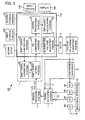
- Fig. 3 is a block diagram which shows a composition of body measurement apparatus 100 according to an embodiment of the present invention.
- Body measurement apparatus 100 measures bioelectrical impedance and a weight of a human subject and computes biological information such as a body fat percentage by calculation based on those measured and preliminarily input personal information such as height, sex, and age.
- Body measurement apparatus 100 includes weight scale 110, first storage portion 120, second storage portion 130, input portion 150, and display 160. These elements are connected to microcontroller 140 through a bus (not shown). Microcontroller 140 acts as a control center which controls the whole apparatus. Microcontroller 140 works with a clock signal supplied from a clock signal generation circuit (not shown). When a power switch (not shown) is turned on, a power circuit powers each of the elements.
- Weight scale 110 measures the weight of the human subject and outputs weight data to microcontroller 140 through the bus.
- First storage portion 120 is a nonvolatile memory such as ROM (Read Only Memory). Control programs for controlling the whole apparatus are stored in first storage 120.
- Microcontroller 140 generates the biological information such as the body fat percentage by executing predetermined calculations in accordance with the control programs.
- Second storage portion 130 is a volatile memory such as DRAM (Dynamic Random Access Memory). Second storage portion 130 acts as a working area used by microcontroller 140 and stores data when the microcontroller executes the predetermined calculations.
- DRAM Dynamic Random Access Memory
- Input portion 150 includes various switches. When the human subject operates the switches, information such as height, age, and sex is input. Display 160 displays measurement results such as weight and body fat percentage and messages promoting the human subject to input various types of information. Display 160 may be made of a liquid crystal display device.
- Input portion 150 includes switches 151 to 155.
- Switch 151 and 152 may act as up and down switches used for inputting a numerical value or selecting a menu.
- Switch 153 and 154 may act as a switch for determining an input state.
- Switch 155 may act as a power switch.
- AD conversion apparatus 1 is incorporated in body measurement apparatus 100.
- AD converting portion 40 is embedded in microcontroller 140.
- Shift signal controlling portion 10 and signal processing portion 50 are realized by executing the predetermined programs in microcontroller 140.
- Microcontroller 140 includes impedance calculating portion 60 and alternating voltage signal generating portion 70.
- Impedance calculating portion 60 calculates impedance based on output digital signals C out outputted from signal processing portion 50.
- Alternating voltage signal generating portion 70 generates a voltage signal having a 50 kHz square wave. More specifically, the 50 kHz constant-voltage square wave is output from a port using a timer function of microcontroller 140.
- alternating voltage signal generating portion 70 is embedded in microcontroller 140, meanwhile the signal may be generated outside microcontroller 140 as a matter of course.
- Filter 3 may be composed of a low-pass or band-pass filter which passes 50 kHz and removes a harmonic component of the 50 kHz voltage signal. As a result, the signal that has been passed through filter 3 is a sine wave.
- Voltage-to-current converting portion 4 converts the voltage signal output from filter 3 to current signal.
- the current signal is supplied in series to reference impedance Z r and biological impedance Z h which are serially connected.
- Reference impedance Z r is known and biological impedance Z h is impedance of the human subject.
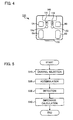
- Body measurement apparatus 100 includes two current electrodes (CE) 5A, 5B and two voltage electrodes (VE) 6A, 6B. As illustrated in Fig. 4 , current electrode 5A is placed corresponding to an anterior portion of a left foot, electrode 6A is placed corresponding to a heel portion of the left foot, electrode 5B is placed corresponding to an anterior portion of a right foot, and electrode 6B is placed corresponding to a heel portion of the right foot.
- CE current electrodes
- VE voltage electrodes
- Signal selecting portion 7 selects terminals T1 and T2 located on both ends of reference impedance Z r or voltage electrodes 6A and 6B for measuring biological impedance Z h .
- Signal receiving portion 8 may be composed of a differential amplifier. The differential amplifier acts as a voltage buffer amplifier with high impedance input. As a result, when terminals T1 and T2 located on both ends of reference impedance Z r are selected by signal selecting portion 7, signal receiving portion 8 outputs voltage V r of reference impedance Z r . Meanwhile, when voltage electrodes 6A and 6B are selected by signal selecting portion 7, signal receiving portion 8 outputs voltage V h of biological impedance Z h .
- Signal receiving portion 8 adjusts signal amplitude according to a dynamic range of shift signal adding portion 30 or AD converting portion 40.
- shift signal generating portion 20 is controlled by shift signal controlling portion 10 and outputs 27 DC voltages as shift signals ⁇ k to shift signal adding portion 30. Intervals of 27 DC voltages are equivalent.
- shift signal generating portion 20 may be composed of a dedicated DA converter, in this embodiment, shift signal generating portion 20 is composed of three ports of microcontroller 140 being controllable with three-state form, a plurality of resistances, and a buffer. Since each of the three ports can take three states, each of which is a high level state, a low level state, or a high impedance state, the three ports can represent 27 states. As a result, 27 DC voltages can be generated as shift signals ⁇ k .
- Shift signal controller 10 controls the states of the three ports of microcontroller 140.
- Shift signal adding portion 30 sets a one-fold gain for the voltage inputted from signal receiving portion 8 and sets gains such that each of 27 shift signals ⁇ k differs by 1/9 LSB from the adjacent shift signals ⁇ k for DC voltages generated in shift signal generating portion 20.
- AD converting portion 40 divides a 50 kHz sine wave into 20 parts per cycle and measures at the 20 phase points.
- Signal processing portion 50 obtains voltages at the phase points of the alternating voltage with higher resolution than the original resolution of AD converting portion 40 using the results of the AD conversion.
- Impedance calculating portion 60 calculates impedance using the high resolution AD conversion results obtained by signal processing portion 50.
- vector components (a resistance component and a reactance component) are obtained by executing synchronous detection using the high resolution AD conversion results at the 20 phase points.
- the synchronous detection is executed for both reference impedance Z r and biological impedance Z h .
- microcontroller 140 controls signal selecting portion 7 to select reference impedance Z r or biological impedance Z h (step S10).
- microcontroller 140 executes an accumulation process (step S20).
- microcontroller 140 sequentially adds 27 shift signals ⁇ k to voltage V r or voltage V h to generate 27 first signals S1, executes AD conversion to convert the signals into 27 second signals S2, and average 27 second signals S2.
- voltage V r and voltage V h can be AD-converted with a resolution which exceeds the minimum resolution of AD converting portion 40.
- An 'A' is a constant for converting a voltage into an AD conversion result code used in AD converting portion 40 and a 'Round' is a function rounding a value outputted from AD converting portion 40 less than 1 LSB.
- This calculation is executed in signal processing portion 50.
- an output signal from signal receiving portion 8 is often rounded and a fraction is disregarded.
- an AD conversion result with a higher resolution than the original resolution of AD converting portion 40 can be obtained by averaging using plural shift signals ⁇ k with 1/9-LSB steps.
- the AD conversion results are accumulated for four times to obtain a stable result. As described above, output digital signals are generated.
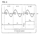
- shift signal controlling portion 10 controls shift signal generating portion 20 to switch 27 shift signals ⁇ 0 , ⁇ 1 , ... , and ⁇ 26 sequentially every interval of the cycle of input analog signal C in .
- AD converting portion 40 executes AD conversion on 20 phase points P 0 , P 1 , ... , and P 19 per one cycle.
- AD converting portion 40 executes AD conversion to convert 27 first signals S1 obtained by adding each of 27 shift signals ⁇ k to input analog signal C in on each phase point into 27 second signals S2 and signal processing portion 50 calculates an average of 27 second signals S2.
- input analog signal C in is converted to output digital signal C out .
- 27 cycles of input analog signal C in are necessary to obtain one-cycle output digital signal C out .
- this process is repeated four times so as to obtain precision output digital signal C out .
- AD converting portion 40 executes AD conversion in synchronization with the alternating-current signal and shift signal controlling portion 10 controls shift signal generating portion 20 so as to switch shrift signals ⁇ k every interval of the alternating-current signal.
- Signal processing portion 50 processes n second signals S2 in each same phase of each interval of the alternating-current signal into output digital signal C out .
- microcontroller 140 executes detection process (step S30). Specifically, vector components (a resistance component and a reactance component) are obtained by executing synchronous detection between output digital signal C out and a 50 kHz current signal. Microcontroller 140 executes impedance calculation to calculate biological impedance Z h in accordance with the above-described voltage comparison method (step S40).
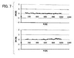
- Fig. 7 shows errors of resistance components and reactance components measured by body measurement apparatus 100 of this embodiment.
- Fig. 8 shows errors of resistance components and reactance components without addition of shift signals ⁇ k as a comparative example.
- the errors can be greatly reduced according to this embodiment.
- it is effective for a general microcontroller in which the AD converting portion 40 is embedded. When such microcontroller is used, the resolution of AD conversion can be greatly improved by adding a minute component.
- AD converting portion 40 may execute AD conversion in synchronization with the alternating-current signal.
- Shift signal controlling portion 10 may control shift signal generating portion 20 to switch 27 shift signals ⁇ k every four intervals of the alternating-current signal.
- Signal processing portion 50 may process 27 x 4 second signals S2 in each same phase points P 0 , P 1 , ... , and P 19 of the alternating-current signal into output digital signal C out . As a result, the number of switching shift signals ⁇ k can be reduced to 27 times.
- n shift signals ⁇ k may exceed the minimum resolution (1 LSB).
- the minimum shift signal ⁇ 0 can take a greater value.
- the minute voltage can be generated easily by setting such that the minimum value of n shift signals ⁇ k exceeds the minimum resolution (1 LSB).
Landscapes
- Engineering & Computer Science (AREA)
- Theoretical Computer Science (AREA)
- Analogue/Digital Conversion (AREA)
- Measurement And Recording Of Electrical Phenomena And Electrical Characteristics Of The Living Body (AREA)
Abstract
Description
- The present invention relates to an analog-to-digital (AD) conversion apparatus, an AD conversion method, and an electronic device.
- Sampling methods used in AD converter are classified broadly into a type of executing sampling with Nyquist frequency and an oversampling type of executing sampling with frequency higher than Nyquist frequency. The oversampling type is intended to enhance a resolution even using an AD converter with a low resolution. Σ - Δ (sigma - delta) type sampling is exemplified as one of the common sampling methods at this time.
- The oversampling type AD converter obtains an intermediate value of output codes by averaging a plurality of AD conversion results sampled with sampling rate higher than the Nyquist frequency. The intermediate value is obtained with various techniques. The original form to obtain the intermediate value utilizes white noise as dither noise.
- The principle to obtain the intermediate value is that the intermediate value of output codes from the AD converter can be obtained by averaging the plurality of the AD conversion results when outputs from the AD converter on each conversion take different values influenced by noise (that is, when outputs keep flickering). This principle has the premise that an average of the noise which causes the flickering is zero, that an effective value of the noise level to the resolution of the AD converter takes from 1/3 LSB (Least Significant Bit) to several LSBs, and that the noise has sufficiently broad bandwidth so that a different result can be obtained on each sampling.
- Patent Document 1:
JP-A-2010-11906 - However, it is often difficult for the AD converter with the low resolution to obtain effects of oversampling since its noise level is far lower than the amplitude of 1 LSB of the AD converter. It is not only technically difficult but also costly to generate white noise with appropriate bandwidth intendedly and stably. Thermal noise of a resistance is widely understood as an example of white noise. The noise voltage vn is represented as Vn = (4kTRΔf)1/2 (k: Boltzmann constant, T: temperature, R: resistance, Δf: bandwidth of noise). Even if R = 1 MΩ, T = 300 K, and Δf = 1 MHz, the noise voltage to be obtained is 0.13 mVrms at most. When a 10bit AD converter has an input voltage range from 0 V to 3 V, the resolution of the 10bit AD converter is approximately 3 mV/LSB. As a result, the thermal noise should be amplified several dozen-fold for practical purposes.
- The frequency band of white noise should be sufficiently higher than signal frequency. If a negative feedback circuit including an operational amplifier for noise amplification is utilized, high frequency-response property corresponding to gain of the operational amplifier is required. Furthermore, particularly low equivalent input noise of the operational amplifier is required for utilizing thermal noise as white noise for sampling. An operational amplifier which satisfies such requirements is far better performing and expensive than a general bluffer amplifier placed before the AD converter for processing an original signal. Moreover, an actual resistive element generates not only theoretical thermal noise but also large 1/f noise, a noise level of the thermal noise may vary depending on temperature, and environmental noise may be superimposed on the thermal noise. Accordingly, it is difficult to generate large amounts of noise intentionally and stably.
- Noise of a Zener diode similar to white noise might be adopted as the sampling noise. However, the Zener diode has problems in that it consumes huge amounts of current, its inter-individual difference is large, and its temperature property is worse than that of the resistance.
- In another problem, in the oversampling with dither noise, if that it is required for improving a resolution of sampling to increase the number of sampling in accordance with the number of bits.
- The Σ - Δ type sampling, which is another type of oversampling, shortens measurement time for sampling in comparison with the oversampling with the dither noise, meanwhile the Σ - Δ type sampling requires massive and complex digital processing. The Σ - Δ type sampling prevails due to current miniaturization technologies. However, semiconductor products specialized for the Σ - Δ type sampling remain expensive. If the digital processing to be executed by hardware in the semiconductor products is executed by software, only a signal having a frequency lower than one several dozenth of clock frequency can be processable. Therefore, it is difficult to execute the Σ - Δ type sampling at high frequency.
- Accordingly, the present invention provides an AD conversion apparatus and an AD conversion method that enables precision AD conversion with simplified composition.
- In accordance with an aspect of the present invention, an AD conversion apparatus includes: a shift signal generating portion configured to generate n shift signals (n is a natural number greater than one) of which amplitudes are different from each other; a compounding portion configured to compound input analog signal and the n shift signals sequentially into n first signals; an AD converting portion configured to execute AD conversion to convert the n first signals into n second signals; and a signal processing portion configured to process the n second signals into output digital signal, in which the shift signal generating portion is configured to generate the n shift signals so that each difference between adjacent shift signals differs from natural number multiples of a minimum resolution of the AD converting portion when the n shift signals are arranged according to the amplitudes.
- In this embodiment, since the first signals are generated by compounding the n shift signals and input analog signal, depending on the amplitudes of the shift signals, some results may exceed the minimum resolution and others may be under the minimum resolution. The n second signals include more precision information than the minimum resolution. As a result, the resolution of AD conversion can be improved by generating the output digital signal based on the second signals. In particular, since each difference between adjacent shift signals is set to differ from natural number multiples of a minimum resolution of the AD converting portion when the n shift signals are arranged according to the amplitudes, the resolution can be improved efficiently.
- In this application, the word 'compounding' includes not only 'addition' but also 'subtraction'.
- Preferably, the shift signal generating portion may be configured to generate the n shift signals so that the differences between the adjacent shift signals are equal to each other and so that the differences are less than the minimum resolution when the n shift signals are arranged according to the amplitudes. In this situation, the n shift signals are separated equivalently from each other, and each of the differences is less than the minimum resolution. As a result, the resolution of AD conversion can be improved by compounding such shift signals and the input analog signal.
- More preferably, the shift signal generating portion may be configured to generate the n shift signals so that a difference between a minimum value and a maximum value of the n shift signals is equal to or greater than the minimum resolution of the AD converting portion. In this situation, given any amplitude of the input signal, at least one of the n first signals exceeds the minimum resolution so that at least one of the n second signals takes a different value from the other second signals. As a result, the resolution of the AD conversion can be further improved.
- Preferably, the signal processing portion may be configured to calculate an average of the n second signals to generate the output digital signals.
- Preferably, the input analog signal may be an alternating-current signal which repeats at a constant interval, one cycle of the alternating-current may correspond to the interval, the AD converting portion may execute AD conversion in synchronization with the alternating-current signal, the AD conversion apparatus may further include a shift signal controlling portion configured to control the shift signal generating portion so as to switch the n shift signals every interval of the alternating-current signal, and the signal processing portion may process the n second signals in each same phase of each interval of the alternating-current signal into the output digital signal.
- When the alternating-current signal which repeats at the constant interval is AD-converted on a plurality of phase points per one interval (cycle) in synchronization with the cycle, the compounding of n shift signals and the alternating-current signal should be done on the same phase point of the alternating-current signal. In this embodiment, the number of switching can be reduced by switching the shift signals every interval of the alternating-current signal.
- Preferably, the input analog signal may be an alternating-current signal which repeats at a constant interval, one cycle of the alternating-current may correspond to the interval, the AD conversion apparatus may be configured to generate the output digital signal based on the n·p intervals (p is a natural number greater than one) of the alternating-current signal, the AD converting portion may execute AD conversion in synchronization with the alternating-current signal, the AD conversion apparatus may further include a shift signal controlling portion configured to control the shift signal generating portion so as to switch the n shift signals every p intervals of the alternating-current signal, and the signal processing portion may process the n·p second signals in each same phase of each interval of the alternating-current signal into the output digital signal.
- In this embodiment, the number of switchings can be greatly reduced by switching the shift signals every p intervals. As a result, time required for AD conversion can be greatly shortened.
- The present invention can certainly be understood as an AD conversion method. In accordance with an aspect of the present invention, an AD conversion method includes: generating n shift signals (n is a natural number greater than one) of which amplitudes are different from each other; compounding input analog signal and the n shift signals sequentially into n first signals; executing AD conversion to convert the n first signals into n second signals; and processing the n second signals into an output digital signal, in which each difference between adjacent shift signals differs from natural number multiples of a minimum resolution of the AD conversion when the n shift signals are arranged according to the amplitudes.
- With reference to the accompanying drawings, embodiments according to the present invention will be described hereinafter. In the drawings:
-
Fig. 1 is a block diagram which shows an AD conversion apparatus according to the first embodiment of the present invention. -
Fig. 2 shows an outline of an AD conversion operation. -
Fig. 3 is a block diagram which shows a body measurement apparatus according to the second embodiment. -
Fig. 4 is a plan view which shows an appearance of the body measurement apparatus. -
Fig. 5 is a flow chart which shows operations of the body measurement apparatus. -
Fig. 6 shows an outline of an AD conversion operation. -
Fig. 7 is a graph which shows errors of resistance components and reactance components measured by the body measurement apparatus. -
Fig. 8 is a graph which shows errors of resistances component and reactance components without addition of shift signals. -
Fig. 9 shows an outline of an AD conversion operation according to a modification. -
Fig. 1 is a block diagram which showsAD conversion apparatus 1 according to an embodiment of the present invention. Input analog signal Cin is supplied toAD conversion apparatus 1.AD conversion apparatus 1 outputs output digital signals Cout.AD conversion apparatus 1 includes shiftsignal generating portion 20 and shiftsignal controlling portion 10. Shiftsignal generating portion 20 generates n (n is a natural number greater than one) shift signals δk (k is an integer from 0 to n-1). Shiftsignal controlling portion 10 controls shiftsignal generating portion 20 to switch n shift signals δk in accordance with a predetermined rule. -
AD conversion apparatus 1 further includes shiftsignal adding portion 30,AD converting portion 40, andsignal processing portion 50.Signal adding portion 30 generates n first signals S1 by adding each of n shift signals δk to input analog signal Cin.AD converting portion 40 executes AD conversion to convert n first signals S1 into n second signals S2.Signal processing portion 50 processes n second signals S2 into output digital signals Cout. -
AD converting portion 40 may generate 10bit second signals S2. Each of first signals S1 is quantized. That is, each offirst signals S 1 is compared with discrete values in which a full scale range (FSR) is equally divided by 210 to be approximated to the closest discrete value. FSR / 210 (= 1 LSB) is a minimum resolution (synonymous to a quantization resolution). An amplitude of first signal S being less than 1 LSB is not possible to be detected and becomes a quantization error. The smaller the minimum resolution is, the higher the accuracy of AD conversion and the cost of the AD converter are. In this embodiment, the minimum resolution can be substantially improved by using shift signals δk. - The amplitudes of n shift signals δk are different from each other. Each of the amplitudes is selected so that each difference between adjacent shift signals δk differs from natural number multiples of the minimum resolution (1 LSB) when n shift signals δk are arranged according to the amplitudes. In this embodiment, each of the amplitudes is set so that the differences between adjacent shift signals δk are equal to each other and so that the differences are less than the minimum resolution when n shift signals δk are arranged according to the amplitudes. "The differences between adjacent shift signals δk are equal to each other" means where n shift signals δk are arranged such that δn-1 δn-2 = δn-2 δn-3 = ... = δ2 - δ1 = δ1 - δ0 when δ0, δ1, ... , δn-2, and δn-1 are arranged in ascending order.
- Input analog signal Cin plus shift signal δk makes
first signal S 1. It is assumed that input analog signal Cin is less than the minimum resolution ofAD converting portion 40 in a following example. When input analog signal Cin is directly supplied toAD converting portion 40, second signal S2 takes the value of zero. On the other hand, first signal S1 to which shift signal δk has been added may occasionally exceed the minimum resolution depending on the amplitudes of input analog signal Cin and shift signal δk. When most of n first signals S1 to each of which each af n shift signals δk has been added exceed the minimum resolution and thus most of second signals S2 take the value of one, input analog signal Cin should be close to the minimum resolution. When most of n first signals S1 do not exceed the minimum resolution and thus most of second signals S2 take the value of zero, input analog signal Cin should be far from the minimum resolution and should be small. That is, the amplitude of input analog signal Cin can be calculated in accordance with the number of n second signals S2 which take the value of one. -
Signal processing portion 50 calculates an average of n second signals S2 to generate output digital signal Cout. As a result, output digital signals Cout to which the discrete values are less than the minimum resolution ofAD converting portion 40 have been assigned can be outputted. - Operations of
AD conversion apparatus 1 will be explained with reference toFig. 2 . In a following example, n is five and five shift signals δk are supplied from shiftsignal generating portion 20. - The operation of
AD converting portion 40 is simplified to be represented as follows:
- A 'Round' is a function which rounds first signal S1 being an analog value to the nearest whole number. For instance, if S1 = 0.4, S2 takes the value of zero and if S1 = 0.6, S2 takes the value of one.
- Shift signals δk (k = 0, ..., n-1) are added to input analog signal Cin and they are averaged. The calculation of
signal processing portion 50 is represented as follows:
- When Cin is equal to 1.2 and Cin is simply supplied to
AD converting portion 40, the output code will be rounded as follows:
- In other words, the original resolution (fractional portion) of
AD converting portion 40 cannot be exceeded without shift signals δk. - Given that n = 5 and δk = {-0.4, -0.2, 0, 0.2, 0.4}, first signals S1 are represented as S1 = {0.8, 1, 1.2, 1.4, 1.6}. Second signals S2, which correspond to five first signals S1, are represented as S2 = {1, 1, 1, 1, 2}.
-
Signal processing portion 50 executes calculation of an average. Output digital signal Cout is represented by the following formula:
- As described above, a higher resolution (decimal fraction) than the original resolution (integer) of
AD converting portion 40 can be obtained by superimposing a plurality of shift signals δk with amplitudes different from the amplitude of the original minimum resolution (1 LSB) ofAD converting portion 40 on input analog signal Cin. - Given that an output digital signal which corresponds to input analog signal Cin is Cout) and an output where input analog signal Cin1 differs by only a minute values (that is, an output of Cin1 + ε) is Cout2, Cout1 and Cout2 are represented as follows:


- When differences Δ between adjacent shift signals are equivalent (δk+1 - δk = Δ), Cout2 and Cour1 are different from each other at least if ε = Δ.
- Cout2 can be represented as follows:

- The worst value of the resolution is represented as follows:

- The last formula means that the resolution is determined depending on a range where shift signals δk are distributed and the number n of shift signals δk. It is preferable for enhancing the resolution that Δ be set to be small and n be set to be large. In practice, code widths of
AD converting portion 40 and step widths of shift signals δk are not uniform and have errors. In view of enhancing precision, it is preferable to adjust nΔ to several LSBs so that the nonuniformity can be equalized. - The second embodiment will be explained using
body measurement apparatus 100 as an example of an electronic device that includes above-describedAD conversion apparatus 1. -
Fig. 3 is a block diagram which shows a composition ofbody measurement apparatus 100 according to an embodiment of the present invention.Body measurement apparatus 100 measures bioelectrical impedance and a weight of a human subject and computes biological information such as a body fat percentage by calculation based on those measured and preliminarily input personal information such as height, sex, and age. -
Body measurement apparatus 100 includesweight scale 110,first storage portion 120,second storage portion 130,input portion 150, anddisplay 160. These elements are connected tomicrocontroller 140 through a bus (not shown).Microcontroller 140 acts as a control center which controls the whole apparatus.Microcontroller 140 works with a clock signal supplied from a clock signal generation circuit (not shown). When a power switch (not shown) is turned on, a power circuit powers each of the elements. -
Weight scale 110 measures the weight of the human subject and outputs weight data tomicrocontroller 140 through the bus.First storage portion 120 is a nonvolatile memory such as ROM (Read Only Memory). Control programs for controlling the whole apparatus are stored infirst storage 120.Microcontroller 140 generates the biological information such as the body fat percentage by executing predetermined calculations in accordance with the control programs. -
Second storage portion 130 is a volatile memory such as DRAM (Dynamic Random Access Memory).Second storage portion 130 acts as a working area used bymicrocontroller 140 and stores data when the microcontroller executes the predetermined calculations. -
Input portion 150 includes various switches. When the human subject operates the switches, information such as height, age, and sex is input.Display 160 displays measurement results such as weight and body fat percentage and messages promoting the human subject to input various types of information.Display 160 may be made of a liquid crystal display device. - More concretely as illustrated in
Fig. 4 ,display 160 is placed on an upper center of a chassis.Input portion 150 includesswitches 151 to 155.Switch Switch Switch 155 may act as a power switch. - Above-describe
AD conversion apparatus 1 is incorporated inbody measurement apparatus 100. In this embodiment,AD converting portion 40 is embedded inmicrocontroller 140. Shiftsignal controlling portion 10 andsignal processing portion 50 are realized by executing the predetermined programs inmicrocontroller 140.Microcontroller 140 includesimpedance calculating portion 60 and alternating voltagesignal generating portion 70. -
Impedance calculating portion 60 calculates impedance based on output digital signals Cout outputted fromsignal processing portion 50. Alternating voltagesignal generating portion 70 generates a voltage signal having a 50 kHz square wave. More specifically, the 50 kHz constant-voltage square wave is output from a port using a timer function ofmicrocontroller 140. In this embodiment, alternating voltagesignal generating portion 70 is embedded inmicrocontroller 140, meanwhile the signal may be generated outsidemicrocontroller 140 as a matter of course. -
Filter 3 may be composed of a low-pass or band-pass filter which passes 50 kHz and removes a harmonic component of the 50 kHz voltage signal. As a result, the signal that has been passed throughfilter 3 is a sine wave. - Voltage-to-
current converting portion 4 converts the voltage signal output fromfilter 3 to current signal. The current signal is supplied in series to reference impedance Zr and biological impedance Zh which are serially connected. Reference impedance Zr is known and biological impedance Zh is impedance of the human subject. -
Body measurement apparatus 100 includes two current electrodes (CE) 5A, 5B and two voltage electrodes (VE) 6A, 6B. As illustrated inFig. 4 ,current electrode 5A is placed corresponding to an anterior portion of a left foot,electrode 6A is placed corresponding to a heel portion of the left foot,electrode 5B is placed corresponding to an anterior portion of a right foot, andelectrode 6B is placed corresponding to a heel portion of the right foot. - Signal selecting
portion 7 selects terminals T1 and T2 located on both ends of reference impedance Zr orvoltage electrodes Signal receiving portion 8 may be composed of a differential amplifier. The differential amplifier acts as a voltage buffer amplifier with high impedance input. As a result, when terminals T1 and T2 located on both ends of reference impedance Zr are selected bysignal selecting portion 7,signal receiving portion 8 outputs voltage Vr of reference impedance Zr. Meanwhile, whenvoltage electrodes signal selecting portion 7,signal receiving portion 8 outputs voltage Vh of biological impedance Zh.Signal receiving portion 8 adjusts signal amplitude according to a dynamic range of shiftsignal adding portion 30 orAD converting portion 40. - An alternating voltage outputted from
signal receiving portion 8 is added with direct-current shift signals δk (described below) and is input toAD converting portion 40. Shiftsignal generating portion 20 is controlled by shiftsignal controlling portion 10 andoutputs 27 DC voltages as shift signals δk to shiftsignal adding portion 30. Intervals of 27 DC voltages are equivalent. Although shiftsignal generating portion 20 may be composed of a dedicated DA converter, in this embodiment, shiftsignal generating portion 20 is composed of three ports ofmicrocontroller 140 being controllable with three-state form, a plurality of resistances, and a buffer. Since each of the three ports can take three states, each of which is a high level state, a low level state, or a high impedance state, the three ports can represent 27 states. As a result, 27 DC voltages can be generated as shift signals δk. -
Shift signal controller 10 controls the states of the three ports ofmicrocontroller 140. Shiftsignal adding portion 30 sets a one-fold gain for the voltage inputted fromsignal receiving portion 8 and sets gains such that each of 27 shift signals δk differs by 1/9 LSB from the adjacent shift signals δk for DC voltages generated in shiftsignal generating portion 20. -
AD converting portion 40 divides a 50 kHz sine wave into 20 parts per cycle and measures at the 20 phase points.Signal processing portion 50 obtains voltages at the phase points of the alternating voltage with higher resolution than the original resolution ofAD converting portion 40 using the results of the AD conversion. -
Impedance calculating portion 60 calculates impedance using the high resolution AD conversion results obtained bysignal processing portion 50. - Specifically, vector components (a resistance component and a reactance component) are obtained by executing synchronous detection using the high resolution AD conversion results at the 20 phase points. The synchronous detection is executed for both reference impedance Zr and biological impedance Zh. Biological impedance Zh is obtained by executing complex arithmetic represented as a following formula in accordance with a voltage comparison method:

- As described above, biological impedance Zh is calculated.
- Operations generating biological impedance in
body measurement apparatus 100 will be explained with reference toFig. 5 . - Firstly,
microcontroller 140 controls signal selectingportion 7 to select reference impedance Zr or biological impedance Zh (step S10). - Next,
microcontroller 140 executes an accumulation process (step S20). In the accumulation process,microcontroller 140 sequentially adds 27 shift signals δk to voltage Vr or voltage Vh to generate 27 first signals S1, executes AD conversion to convert the signals into 27 second signals S2, and average 27 second signals S2. As a result, voltage Vr and voltage Vh can be AD-converted with a resolution which exceeds the minimum resolution ofAD converting portion 40. - AD conversion operations will be explained specifically. Given that a output signal from
signal receiving portion 8 is Vsig and DC voltages outputted from shiftsignal generating portion 20 are Δk (k = 0,..., 26), AD conversion results Ck are represented as follows:
- An 'A' is a constant for converting a voltage into an AD conversion result code used in
AD converting portion 40 and a 'Round' is a function rounding a value outputted fromAD converting portion 40 less than 1 LSB. - Given that Csig is equal to A·Vsig and δk is equal to A·Δk, the above formula is represented as follows:

- Final AD conversion result CT is an average value of AD conversion results Ck corresponding to 27 DC voltages and is represented as follows:

- This calculation is executed in
signal processing portion 50. Conventionally an output signal fromsignal receiving portion 8 is often rounded and a fraction is disregarded. In this embodiment, an AD conversion result with a higher resolution than the original resolution ofAD converting portion 40 can be obtained by averaging using plural shift signals δk with 1/9-LSB steps. - For reducing an amount of calculation, following cumulative value CT' may be used.

- The AD conversion results are accumulated for four times to obtain a stable result. As described above, output digital signals are generated.
- With reference to
Fig. 6 , it will be explained of a relationship among sine-wave input analog signal Cin which is supplied to shiftsignal adding portion 30, shift signals δk, and 20 phase points per one cycle inAD converting portion 40. - To generate 27 DC voltages as shift signals δk, shift
signal controlling portion 10 controls shiftsignal generating portion 20 to switch 27 shift signals δ0, δ1, ... , and δ26 sequentially every interval of the cycle of input analog signal Cin. -
AD converting portion 40 executes AD conversion on 20 phase points P0, P1, ... , and P19 per one cycle.AD converting portion 40 executes AD conversion to convert 27 first signals S1 obtained by adding each of 27 shift signals δk to input analog signal Cin on each phase point into 27 second signals S2 andsignal processing portion 50 calculates an average of 27 second signals S2. As a result, input analog signal Cin is converted to output digital signal Cout. In this case, 27 cycles of input analog signal Cin are necessary to obtain one-cycle output digital signal Cout. In this embodiment, this process is repeated four times so as to obtain precision output digital signal Cout. - When input analog signal Cin is an alternating-current signal which repeats at a constant interval,
AD converting portion 40 executes AD conversion in synchronization with the alternating-current signal and shiftsignal controlling portion 10 controls shiftsignal generating portion 20 so as to switch shrift signals δk every interval of the alternating-current signal.Signal processing portion 50 processes n second signals S2 in each same phase of each interval of the alternating-current signal into output digital signal Cout. - Again, this will be explained with reference to
Fig. 5 . After step S20,microcontroller 140 executes detection process (step S30). Specifically, vector components (a resistance component and a reactance component) are obtained by executing synchronous detection between output digital signal Cout and a 50 kHz current signal.Microcontroller 140 executes impedance calculation to calculate biological impedance Zh in accordance with the above-described voltage comparison method (step S40). -
Fig. 7 shows errors of resistance components and reactance components measured bybody measurement apparatus 100 of this embodiment.Fig. 8 shows errors of resistance components and reactance components without addition of shift signals δk as a comparative example. As these figures show, the errors can be greatly reduced according to this embodiment. Particularly, it is effective for a general microcontroller in which theAD converting portion 40 is embedded. When such microcontroller is used, the resolution of AD conversion can be greatly improved by adding a minute component. - The present invention is not limited to the above-described embodiments. For example, the following modifications are possible.
- (1) In the above-described second embodiment, input analog signal Cin is the alternating-current signal which repeats at the constant interval. When 27 shift signals δk are generated, switching of shift signals δk are executed in 27 cycles (intervals) by switching shift signals δk every interval of the cycle of input analog signal Cin. To enhance accuracy, one-cycle output digital signal Cout may be obtained by repeating the 27-cycle set for four times and averaging the repeated results.
- In the above-described embodiment, it is required to switch shift signals δk for 4 x 27 times as a whole. Since it takes time to switch shift signals δk, it is preferable that the number of switchings be as small as possible. Owing to a floating capacitance and a wiring resistance, a transmission channel from shift
signal generating portion 20 to shiftsignal adding portion 30 is equivalent to a low-pass filter. As a result, it takes time to reflect an effect of switching shift signals δk in an addition result with accuracy. - In view of the above conditions, shift signals δk may be switched as shown in
Fig. 9 . That is, it is assumed that input analog signal Cin is an alternating-current signal which repeats at a constant interval and output digital signal Cout is generated based on n·p intervals (p is a natural number greater than one) of the cycle of the alternating-current signal. In the example shown inFig. 9 , n = 27 and p = 4.AD converting portion 40 may execute AD conversion in synchronization with the alternating-current signal. Shiftsignal controlling portion 10 may control shiftsignal generating portion 20 to switch 27 shift signals δk every four intervals of the alternating-current signal.Signal processing portion 50 may process 27 x 4 second signals S2 in each same phase points P0, P1, ... , and P19 of the alternating-current signal into output digital signal Cout. As a result, the number of switching shift signals δk can be reduced to 27 times. - (2) In the above-described embodiments, shift
signal adding portion 30 generates first signals S by adding each of shift signals δk to input analog signal Cin. On the other hand, first signals S1 may be generated by subtracting each of shift signals δk from input analog signal Cin. In summary, first signals S1 may be generated by compounding input analog signal Cin and shift signals δk. - (3) In the above-described embodiments, the amplitudes of n shift signals δk are different from each other and n shift signals δk are selected so that the differences between the adjacent shift signals are equal to each other and that the differences are less than the minimum resolution when n shift signals δk are arranged according to the amplitudes. On the other hand, parts of n shift signals δk may correspond to natural number multiples of the minimum resolution (1 LSB).
- The minimum value of n shift signals δk may exceed the minimum resolution (1 LSB). For example, n shift signals δk may be set equivalent, that is Δ = δk - δk-1, and δ0 = 1.1 LSB, δ1 = 1.3 LSB, δ2 = 1.5 LSB, δ3 = 1.7 LSB, δ4 = 1.9 LSB, and δ5 = 2.1 LSB given that Δ = 0.2 LSB and n = 5. In comparison in the case in which shift signals δk are set such that δ0 = 0.1 LSB, δ1 = 0.3 LSB, δ2 = 0.5 LSB, δ3 = 0.7 LSB, δ4 = 0.9 LSB, and δ5 = 1.1 LSB, the minimum shift signal δ0 can take a greater value. In general, it is difficult to generate a minute voltage precisely due to noise. The minute voltage can be generated easily by setting such that the minimum value of n shift signals δk exceeds the minimum resolution (1 LSB).
- When the difference between the minimum value (δ0 = 1.1 LSB) and the maximum value (δ5 = 2.1 LSB) of n shift signals δk is equal to or more than the minimum resolution of
AD converting portion 40 as this example, at least one second signal S2 differs from the other second signals S2 by adding each of n shift signals δk to input analog signal Cin with any amplitude. As a result, the resolution of AD conversion can be improved.
Claims (8)
- An AD conversion apparatus comprising:a shift signal generating portion configured to generate n shift signals (n is a natural number greater than one) of which amplitudes are different from each other;a compounding portion configured to compound input analog signal and the n shift signals sequentially into n first signals;an AD converting portion configured to execute AD conversion to convert the n first signals into n second signals; anda signal processing portion configured to process the n second signals into output digital signal,wherein the shift signal generating portion is configured to generate the n shift signals so that each difference between adjacent shift signals differs from natural number multiples of a minimum resolution of the AD converting portion when then shift signals are arranged according to the amplitudes.
- The AD conversion apparatus according to claim 1, wherein the shift signal generating portion is configured to generate the n shift signals so that the differences between the adjacent shift signals are equal to each other and so that the differences are less than the minimum resolution when the n shift signals are arranged according to the amplitudes.
- The AD conversion apparatus according to claim 2, wherein the shift signal generating portion is configured to generate the n shift signals so that a difference between a minimum value and a maximum value of the n shift signals is equal to or greater than the minimum resolution of the AD converting portion.
- The AD conversion apparatus according to any one of claims 1 to 3, wherein the signal processing portion is configured to calculate an average of the n second signals to generate the output digital signals.
- The AD conversion apparatus according to any one of claims 1 to 4, wherein
the input analog signal is an alternating-current signal, which repeats at a constant interval,
one cycle of the alternating-current corresponding to the interval,
the AD converting portion executing AD conversion in synchronization with the alternating-current signal,
the AD conversion apparatus further comprising a shift signal controlling portion configured to control the shift signal generating portion so as to switch the n shift signals every interval of the alteniating-current signal, and
the signal processing portion processing the n second signals in each same phase of each interval of the alternating-current signal into the output digital signal. - The AD conversion apparatus according to any one of claims 1 to 3, wherein
the input analog signal is an alternating-current signal that repeats at a constant interval,
one cycle of the alternating-current corresponding to the interval,
the AD conversion apparatus being configured to generate the output digital signal based on the n·p intervals (p is a natural number greater than one) of the alternating-current signal,
the AD converting portion executing AD conversion in synchronization with the alternating-current signal,
the AD conversion apparatus further comprising a shift signal controlling portion configured to control the shift signal generating portion so as to switch the n shift signals every p intervals of the alternating-current signal, and
the signal processing portion processing the n·p second signals in each same phase of each interval of the alternating-current signal into the output digital signal. - An electronic device comprises the AD conversion apparatus according to any one of claims 1 to 6.
- An AD conversion method comprising:generating n shift signals (n is a natural number greater than one) of which amplitudes are different from each other;compounding input analog signal and they shift signals sequentially into n first signals;executing AD conversion to convert the n first signals into n second signals; andprocessing the n second signals into output digital signal,wherein each difference between adjacent shift signals differs from natural number multiples of a minimum resolution of the AD conversion when the n shift signals are arranged according to the amplitudes.
Applications Claiming Priority (1)
| Application Number | Priority Date | Filing Date | Title |
|---|---|---|---|
| JP2010154623A JP5679412B2 (en) | 2010-07-07 | 2010-07-07 | AD conversion apparatus, AD conversion method, and electronic apparatus |
Publications (3)
| Publication Number | Publication Date |
|---|---|
| EP2405578A2 true EP2405578A2 (en) | 2012-01-11 |
| EP2405578A3 EP2405578A3 (en) | 2012-12-12 |
| EP2405578B1 EP2405578B1 (en) | 2018-01-24 |
Family
ID=44118278
Family Applications (1)
| Application Number | Title | Priority Date | Filing Date |
|---|---|---|---|
| EP11168860.2A Active EP2405578B1 (en) | 2010-07-07 | 2011-06-07 | Analog-to-digital conversion apparatus, analog-to-digital conversion method, and electronic device |
Country Status (5)
| Country | Link |
|---|---|
| US (1) | US8416108B2 (en) |
| EP (1) | EP2405578B1 (en) |
| JP (1) | JP5679412B2 (en) |
| KR (1) | KR101175046B1 (en) |
| CN (2) | CN202364202U (en) |
Families Citing this family (5)
| Publication number | Priority date | Publication date | Assignee | Title |
|---|---|---|---|---|
| JP5679412B2 (en) * | 2010-07-07 | 2015-03-04 | 株式会社タニタ | AD conversion apparatus, AD conversion method, and electronic apparatus |
| LU92212B1 (en) * | 2013-06-11 | 2014-12-12 | Iee Sarl | Method for converting an analog signal into a digital signal |
| US8994570B1 (en) * | 2013-09-26 | 2015-03-31 | Cambridge Silicon Radio Limited | Multi-level quantizers and analogue-to-digital converters |
| CN110546468B (en) | 2017-04-01 | 2026-03-17 | 范颂尼控股有限公司 | Sensing and control devices and methods for weight measurement equipment |
| JP7412551B2 (en) * | 2019-10-23 | 2024-01-12 | ホアウェイ・テクノロジーズ・カンパニー・リミテッド | Adaptive correlated multiple sampling with input signal level shift |
Family Cites Families (21)
| Publication number | Priority date | Publication date | Assignee | Title |
|---|---|---|---|---|
| US4710747A (en) * | 1984-03-09 | 1987-12-01 | Fairchild Semiconductor Corporation | Method and apparatus for improving the accuracy and resolution of an analog-to-digital converter (ADC) |
| JPS6341936U (en) * | 1986-09-03 | 1988-03-19 | ||
| JP2533062Y2 (en) * | 1987-07-03 | 1997-04-16 | ヤマハ株式会社 | Analog-to-digital conversion circuit |
| JPH02260821A (en) * | 1989-03-31 | 1990-10-23 | Mitsubishi Motors Corp | A/d conversion system |
| JPH0821857B2 (en) * | 1989-11-08 | 1996-03-04 | ティアツク株式会社 | Analog-digital conversion method |
| JP2626352B2 (en) * | 1991-09-27 | 1997-07-02 | ティーディーケイ株式会社 | A / D converter |
| JPH0575461A (en) * | 1991-09-11 | 1993-03-26 | Nikon Corp | Signal processor |
| US5552783A (en) * | 1994-03-31 | 1996-09-03 | Hewlett-Packard Company | Constant current voltage restoration |
| JP3684655B2 (en) * | 1996-03-13 | 2005-08-17 | ソニー株式会社 | Digital signal processor |
| US5825318A (en) * | 1996-12-19 | 1998-10-20 | Quantum Corporation | Data and servo sampling in synchronous data detection channel |
| US6507449B1 (en) * | 1998-12-09 | 2003-01-14 | Marvell International, Ltd. | Digital servo demodulator with synchronous dithering and method |
| US7233746B2 (en) * | 2002-01-30 | 2007-06-19 | Blake James N | Wide dynamic range sensor signal processing method & circuitry for analog and digital information signals |
| US7075466B1 (en) * | 2003-05-20 | 2006-07-11 | Pixelworks, Inc. | System and method for improving performance of an analog to digital converter |
| JP2005249690A (en) * | 2004-03-05 | 2005-09-15 | Agilent Technol Inc | Signal holding method, analog / digital conversion method, signal holding apparatus, analog / digital conversion apparatus, and signal observation apparatus |
| JP4502672B2 (en) * | 2004-03-15 | 2010-07-14 | 日本航空電子工業株式会社 | Closed loop fiber optic gyro |
| JP2007266951A (en) * | 2006-03-28 | 2007-10-11 | Toshiba Corp | Analog to digital converter |
| CN101482890B (en) * | 2008-01-10 | 2011-11-16 | 北京芯慧同用微电子技术有限责任公司 | Circuit simulation apparatus and method |
| JP5020157B2 (en) * | 2008-04-25 | 2012-09-05 | 日本電信電話株式会社 | Analog / digital conversion circuit |
| JP5242260B2 (en) | 2008-07-01 | 2013-07-24 | 株式会社タニタ | Body composition measuring device |
| JP5679412B2 (en) * | 2010-07-07 | 2015-03-04 | 株式会社タニタ | AD conversion apparatus, AD conversion method, and electronic apparatus |
| US8289198B2 (en) * | 2010-11-02 | 2012-10-16 | Texas Instruments Incorporated | Low power bit switches and method for high-voltage input SAR ADC |
-
2010
- 2010-07-07 JP JP2010154623A patent/JP5679412B2/en active Active
-
2011
- 2011-06-07 EP EP11168860.2A patent/EP2405578B1/en active Active
- 2011-06-16 US US13/161,994 patent/US8416108B2/en active Active
- 2011-07-06 KR KR1020110066977A patent/KR101175046B1/en active Active
- 2011-07-07 CN CN2011202434204U patent/CN202364202U/en not_active Expired - Fee Related
- 2011-07-07 CN CN201110193585.XA patent/CN102340311B/en active Active
Non-Patent Citations (1)
| Title |
|---|
| None |
Also Published As
| Publication number | Publication date |
|---|---|
| CN102340311B (en) | 2014-11-05 |
| KR20120004941A (en) | 2012-01-13 |
| US8416108B2 (en) | 2013-04-09 |
| EP2405578B1 (en) | 2018-01-24 |
| JP2012019320A (en) | 2012-01-26 |
| KR101175046B1 (en) | 2012-08-17 |
| EP2405578A3 (en) | 2012-12-12 |
| CN102340311A (en) | 2012-02-01 |
| US20120007761A1 (en) | 2012-01-12 |
| JP5679412B2 (en) | 2015-03-04 |
| CN202364202U (en) | 2012-08-01 |
Similar Documents
| Publication | Publication Date | Title |
|---|---|---|
| US8416108B2 (en) | Analog-to-digital conversion apparatus, analog-to-digital conversion method, and electronic device | |
| US9871442B2 (en) | Zero-offset voltage feedback for AC power supplies | |
| US8672542B2 (en) | High resolution measurement of thermistor thermometry signals with wide dynamic range | |
| KR101040589B1 (en) | Power calibration method according to temperature change of electronic electricity meter | |
| JP5870699B2 (en) | Sensor output correction circuit, sensor output correction device, and sensor output correction method | |
| EP0483846A2 (en) | Analog-to-digital converter circuit | |
| CN102684696B (en) | The testing apparatus of A/D converter and method of testing | |
| KR20090085283A (en) | Error correction device and method of analog-to-digital converter | |
| JP2007208984A (en) | Measurement and correction of nonlinearity of internal multi-bit analog / digital converter in Delta-Sigma A / D converter | |
| US12224762B2 (en) | Measurement unit configured to provide a measurement result value | |
| US11936396B2 (en) | AD converter with self-calibration function | |
| JP2003032108A (en) | Linearity compensation device and linearity compensation method | |
| JP2013131838A (en) | D/a converter system and testing apparatus using the same | |
| US8860592B2 (en) | Signal generating circuit | |
| US12413238B2 (en) | Measurement unit configured to provide a measurement result value using calculated values | |
| JP6945770B2 (en) | Error detection circuit | |
| JPH04370769A (en) | Correction method of voltage and current signal by using a/d converter | |
| RU2292642C1 (en) | Method for integrating analog-to-digital voltage conversion | |
| US20140098847A1 (en) | Test circuit | |
| CN118801884B (en) | Analog-to-digital conversion device, digital signal calibration method and device | |
| JP4799307B2 (en) | Power measuring device | |
| CN120956265A (en) | Error calibration methods, devices, equipment, and storage media for analog-to-digital converter (ADC) circuits. | |
| JP5763558B2 (en) | Measuring apparatus and measuring method using the same | |
| JP6071721B2 (en) | measuring device | |
| JP2017135643A (en) | Digital-to-analog conversion device |
Legal Events
| Date | Code | Title | Description |
|---|---|---|---|
| AK | Designated contracting states |
Kind code of ref document: A2 Designated state(s): AL AT BE BG CH CY CZ DE DK EE ES FI FR GB GR HR HU IE IS IT LI LT LU LV MC MK MT NL NO PL PT RO RS SE SI SK SM TR |
|
| AX | Request for extension of the european patent |
Extension state: BA ME |
|
| PUAI | Public reference made under article 153(3) epc to a published international application that has entered the european phase |
Free format text: ORIGINAL CODE: 0009012 |
|
| PUAL | Search report despatched |
Free format text: ORIGINAL CODE: 0009013 |
|
| RIC1 | Information provided on ipc code assigned before grant |
Ipc: H03M 1/20 20060101ALI20121025BHEP Ipc: H03M 1/12 20060101ALN20121025BHEP Ipc: H03M 1/06 20060101AFI20121025BHEP |
|
| RIC1 | Information provided on ipc code assigned before grant |
Ipc: H03M 1/12 20060101ALN20121101BHEP Ipc: H03M 1/06 20060101AFI20121101BHEP Ipc: H03M 1/20 20060101ALI20121101BHEP |
|
| AK | Designated contracting states |
Kind code of ref document: A3 Designated state(s): AL AT BE BG CH CY CZ DE DK EE ES FI FR GB GR HR HU IE IS IT LI LT LU LV MC MK MT NL NO PL PT RO RS SE SI SK SM TR |
|
| AX | Request for extension of the european patent |
Extension state: BA ME |
|
| 17P | Request for examination filed |
Effective date: 20130607 |
|
| RBV | Designated contracting states (corrected) |
Designated state(s): AL AT BE BG CH CY CZ DE DK EE ES FI FR GB GR HR HU IE IS IT LI LT LU LV MC MK MT NL NO PL PT RO RS SE SI SK SM TR |
|
| 17Q | First examination report despatched |
Effective date: 20170221 |
|
| GRAP | Despatch of communication of intention to grant a patent |
Free format text: ORIGINAL CODE: EPIDOSNIGR1 |
|
| RIC1 | Information provided on ipc code assigned before grant |
Ipc: H03M 1/12 20060101ALN20170825BHEP Ipc: H03M 1/06 20060101AFI20170825BHEP Ipc: H03M 1/20 20060101ALI20170825BHEP |
|
| INTG | Intention to grant announced |
Effective date: 20170922 |
|
| GRAS | Grant fee paid |
Free format text: ORIGINAL CODE: EPIDOSNIGR3 |
|
| RAP1 | Party data changed (applicant data changed or rights of an application transferred) |
Owner name: TANITA CORPORATION |
|
| RIN1 | Information on inventor provided before grant (corrected) |
Inventor name: NAKADA, MASATO |
|
| GRAA | (expected) grant |
Free format text: ORIGINAL CODE: 0009210 |
|
| AK | Designated contracting states |
Kind code of ref document: B1 Designated state(s): AL AT BE BG CH CY CZ DE DK EE ES FI FR GB GR HR HU IE IS IT LI LT LU LV MC MK MT NL NO PL PT RO RS SE SI SK SM TR |
|
| REG | Reference to a national code |
Ref country code: GB Ref legal event code: FG4D |
|
| REG | Reference to a national code |
Ref country code: CH Ref legal event code: EP |
|
| REG | Reference to a national code |
Ref country code: AT Ref legal event code: REF Ref document number: 966319 Country of ref document: AT Kind code of ref document: T Effective date: 20180215 |
|
| REG | Reference to a national code |
Ref country code: IE Ref legal event code: FG4D |
|
| REG | Reference to a national code |
Ref country code: DE Ref legal event code: R096 Ref document number: 602011045234 Country of ref document: DE |
|
| REG | Reference to a national code |
Ref country code: NL Ref legal event code: MP Effective date: 20180124 |
|
| REG | Reference to a national code |
Ref country code: LT Ref legal event code: MG4D |
|
| REG | Reference to a national code |
Ref country code: AT Ref legal event code: MK05 Ref document number: 966319 Country of ref document: AT Kind code of ref document: T Effective date: 20180124 |
|
| REG | Reference to a national code |
Ref country code: FR Ref legal event code: PLFP Year of fee payment: 8 |
|
| PG25 | Lapsed in a contracting state [announced via postgrant information from national office to epo] |
Ref country code: NL Free format text: LAPSE BECAUSE OF FAILURE TO SUBMIT A TRANSLATION OF THE DESCRIPTION OR TO PAY THE FEE WITHIN THE PRESCRIBED TIME-LIMIT Effective date: 20180124 |
|
| PG25 | Lapsed in a contracting state [announced via postgrant information from national office to epo] |
Ref country code: ES Free format text: LAPSE BECAUSE OF FAILURE TO SUBMIT A TRANSLATION OF THE DESCRIPTION OR TO PAY THE FEE WITHIN THE PRESCRIBED TIME-LIMIT Effective date: 20180124 Ref country code: CY Free format text: LAPSE BECAUSE OF FAILURE TO SUBMIT A TRANSLATION OF THE DESCRIPTION OR TO PAY THE FEE WITHIN THE PRESCRIBED TIME-LIMIT Effective date: 20180124 Ref country code: NO Free format text: LAPSE BECAUSE OF FAILURE TO SUBMIT A TRANSLATION OF THE DESCRIPTION OR TO PAY THE FEE WITHIN THE PRESCRIBED TIME-LIMIT Effective date: 20180424 Ref country code: FI Free format text: LAPSE BECAUSE OF FAILURE TO SUBMIT A TRANSLATION OF THE DESCRIPTION OR TO PAY THE FEE WITHIN THE PRESCRIBED TIME-LIMIT Effective date: 20180124 Ref country code: LT Free format text: LAPSE BECAUSE OF FAILURE TO SUBMIT A TRANSLATION OF THE DESCRIPTION OR TO PAY THE FEE WITHIN THE PRESCRIBED TIME-LIMIT Effective date: 20180124 Ref country code: HR Free format text: LAPSE BECAUSE OF FAILURE TO SUBMIT A TRANSLATION OF THE DESCRIPTION OR TO PAY THE FEE WITHIN THE PRESCRIBED TIME-LIMIT Effective date: 20180124 |
|
| PG25 | Lapsed in a contracting state [announced via postgrant information from national office to epo] |
Ref country code: BG Free format text: LAPSE BECAUSE OF FAILURE TO SUBMIT A TRANSLATION OF THE DESCRIPTION OR TO PAY THE FEE WITHIN THE PRESCRIBED TIME-LIMIT Effective date: 20180424 Ref country code: AT Free format text: LAPSE BECAUSE OF FAILURE TO SUBMIT A TRANSLATION OF THE DESCRIPTION OR TO PAY THE FEE WITHIN THE PRESCRIBED TIME-LIMIT Effective date: 20180124 Ref country code: RS Free format text: LAPSE BECAUSE OF FAILURE TO SUBMIT A TRANSLATION OF THE DESCRIPTION OR TO PAY THE FEE WITHIN THE PRESCRIBED TIME-LIMIT Effective date: 20180124 Ref country code: SE Free format text: LAPSE BECAUSE OF FAILURE TO SUBMIT A TRANSLATION OF THE DESCRIPTION OR TO PAY THE FEE WITHIN THE PRESCRIBED TIME-LIMIT Effective date: 20180124 Ref country code: IS Free format text: LAPSE BECAUSE OF FAILURE TO SUBMIT A TRANSLATION OF THE DESCRIPTION OR TO PAY THE FEE WITHIN THE PRESCRIBED TIME-LIMIT Effective date: 20180524 Ref country code: LV Free format text: LAPSE BECAUSE OF FAILURE TO SUBMIT A TRANSLATION OF THE DESCRIPTION OR TO PAY THE FEE WITHIN THE PRESCRIBED TIME-LIMIT Effective date: 20180124 Ref country code: PL Free format text: LAPSE BECAUSE OF FAILURE TO SUBMIT A TRANSLATION OF THE DESCRIPTION OR TO PAY THE FEE WITHIN THE PRESCRIBED TIME-LIMIT Effective date: 20180124 Ref country code: GR Free format text: LAPSE BECAUSE OF FAILURE TO SUBMIT A TRANSLATION OF THE DESCRIPTION OR TO PAY THE FEE WITHIN THE PRESCRIBED TIME-LIMIT Effective date: 20180425 |
|
| REG | Reference to a national code |
Ref country code: DE Ref legal event code: R097 Ref document number: 602011045234 Country of ref document: DE |
|
| PG25 | Lapsed in a contracting state [announced via postgrant information from national office to epo] |
Ref country code: RO Free format text: LAPSE BECAUSE OF FAILURE TO SUBMIT A TRANSLATION OF THE DESCRIPTION OR TO PAY THE FEE WITHIN THE PRESCRIBED TIME-LIMIT Effective date: 20180124 Ref country code: IT Free format text: LAPSE BECAUSE OF FAILURE TO SUBMIT A TRANSLATION OF THE DESCRIPTION OR TO PAY THE FEE WITHIN THE PRESCRIBED TIME-LIMIT Effective date: 20180124 Ref country code: EE Free format text: LAPSE BECAUSE OF FAILURE TO SUBMIT A TRANSLATION OF THE DESCRIPTION OR TO PAY THE FEE WITHIN THE PRESCRIBED TIME-LIMIT Effective date: 20180124 Ref country code: AL Free format text: LAPSE BECAUSE OF FAILURE TO SUBMIT A TRANSLATION OF THE DESCRIPTION OR TO PAY THE FEE WITHIN THE PRESCRIBED TIME-LIMIT Effective date: 20180124 |
|
| PG25 | Lapsed in a contracting state [announced via postgrant information from national office to epo] |
Ref country code: DK Free format text: LAPSE BECAUSE OF FAILURE TO SUBMIT A TRANSLATION OF THE DESCRIPTION OR TO PAY THE FEE WITHIN THE PRESCRIBED TIME-LIMIT Effective date: 20180124 Ref country code: SM Free format text: LAPSE BECAUSE OF FAILURE TO SUBMIT A TRANSLATION OF THE DESCRIPTION OR TO PAY THE FEE WITHIN THE PRESCRIBED TIME-LIMIT Effective date: 20180124 Ref country code: CZ Free format text: LAPSE BECAUSE OF FAILURE TO SUBMIT A TRANSLATION OF THE DESCRIPTION OR TO PAY THE FEE WITHIN THE PRESCRIBED TIME-LIMIT Effective date: 20180124 Ref country code: SK Free format text: LAPSE BECAUSE OF FAILURE TO SUBMIT A TRANSLATION OF THE DESCRIPTION OR TO PAY THE FEE WITHIN THE PRESCRIBED TIME-LIMIT Effective date: 20180124 |
|
| PLBE | No opposition filed within time limit |
Free format text: ORIGINAL CODE: 0009261 |
|
| STAA | Information on the status of an ep patent application or granted ep patent |
Free format text: STATUS: NO OPPOSITION FILED WITHIN TIME LIMIT |
|
| 26N | No opposition filed |
Effective date: 20181025 |
|
| REG | Reference to a national code |
Ref country code: CH Ref legal event code: PL |
|
| PG25 | Lapsed in a contracting state [announced via postgrant information from national office to epo] |
Ref country code: SI Free format text: LAPSE BECAUSE OF FAILURE TO SUBMIT A TRANSLATION OF THE DESCRIPTION OR TO PAY THE FEE WITHIN THE PRESCRIBED TIME-LIMIT Effective date: 20180124 |
|
| REG | Reference to a national code |
Ref country code: BE Ref legal event code: MM Effective date: 20180630 |
|
| REG | Reference to a national code |
Ref country code: IE Ref legal event code: MM4A |
|
| PG25 | Lapsed in a contracting state [announced via postgrant information from national office to epo] |
Ref country code: MC Free format text: LAPSE BECAUSE OF FAILURE TO SUBMIT A TRANSLATION OF THE DESCRIPTION OR TO PAY THE FEE WITHIN THE PRESCRIBED TIME-LIMIT Effective date: 20180124 Ref country code: LU Free format text: LAPSE BECAUSE OF NON-PAYMENT OF DUE FEES Effective date: 20180607 |
|
| PG25 | Lapsed in a contracting state [announced via postgrant information from national office to epo] |
Ref country code: CH Free format text: LAPSE BECAUSE OF NON-PAYMENT OF DUE FEES Effective date: 20180630 Ref country code: LI Free format text: LAPSE BECAUSE OF NON-PAYMENT OF DUE FEES Effective date: 20180630 Ref country code: IE Free format text: LAPSE BECAUSE OF NON-PAYMENT OF DUE FEES Effective date: 20180607 |
|
| PG25 | Lapsed in a contracting state [announced via postgrant information from national office to epo] |
Ref country code: BE Free format text: LAPSE BECAUSE OF NON-PAYMENT OF DUE FEES Effective date: 20180630 |
|
| PG25 | Lapsed in a contracting state [announced via postgrant information from national office to epo] |
Ref country code: MT Free format text: LAPSE BECAUSE OF NON-PAYMENT OF DUE FEES Effective date: 20180607 |
|
| PG25 | Lapsed in a contracting state [announced via postgrant information from national office to epo] |
Ref country code: TR Free format text: LAPSE BECAUSE OF FAILURE TO SUBMIT A TRANSLATION OF THE DESCRIPTION OR TO PAY THE FEE WITHIN THE PRESCRIBED TIME-LIMIT Effective date: 20180124 |
|
| PG25 | Lapsed in a contracting state [announced via postgrant information from national office to epo] |
Ref country code: HU Free format text: LAPSE BECAUSE OF FAILURE TO SUBMIT A TRANSLATION OF THE DESCRIPTION OR TO PAY THE FEE WITHIN THE PRESCRIBED TIME-LIMIT; INVALID AB INITIO Effective date: 20110607 Ref country code: PT Free format text: LAPSE BECAUSE OF FAILURE TO SUBMIT A TRANSLATION OF THE DESCRIPTION OR TO PAY THE FEE WITHIN THE PRESCRIBED TIME-LIMIT Effective date: 20180124 |
|
| PG25 | Lapsed in a contracting state [announced via postgrant information from national office to epo] |
Ref country code: MK Free format text: LAPSE BECAUSE OF NON-PAYMENT OF DUE FEES Effective date: 20180124 |
|
| P01 | Opt-out of the competence of the unified patent court (upc) registered |
Effective date: 20230509 |
|
| PGFP | Annual fee paid to national office [announced via postgrant information from national office to epo] |
Ref country code: DE Payment date: 20250618 Year of fee payment: 15 |
|
| PGFP | Annual fee paid to national office [announced via postgrant information from national office to epo] |
Ref country code: GB Payment date: 20250618 Year of fee payment: 15 |
|
| PGFP | Annual fee paid to national office [announced via postgrant information from national office to epo] |
Ref country code: FR Payment date: 20250624 Year of fee payment: 15 |