EP2403163A1 - Method and system for generation of QAM formats for applications in optical communication - Google Patents
Method and system for generation of QAM formats for applications in optical communication Download PDFInfo
- Publication number
- EP2403163A1 EP2403163A1 EP10305702A EP10305702A EP2403163A1 EP 2403163 A1 EP2403163 A1 EP 2403163A1 EP 10305702 A EP10305702 A EP 10305702A EP 10305702 A EP10305702 A EP 10305702A EP 2403163 A1 EP2403163 A1 EP 2403163A1
- Authority
- EP
- European Patent Office
- Prior art keywords
- optical
- output
- wavelength converter
- input
- optical wavelength
- Prior art date
- Legal status (The legal status is an assumption and is not a legal conclusion. Google has not performed a legal analysis and makes no representation as to the accuracy of the status listed.)
- Granted
Links
Images

Classifications
-
- H—ELECTRICITY
- H04—ELECTRIC COMMUNICATION TECHNIQUE
- H04B—TRANSMISSION
- H04B10/00—Transmission systems employing electromagnetic waves other than radio-waves, e.g. infrared, visible or ultraviolet light, or employing corpuscular radiation, e.g. quantum communication
- H04B10/50—Transmitters
- H04B10/516—Details of coding or modulation
-
- H—ELECTRICITY
- H04—ELECTRIC COMMUNICATION TECHNIQUE
- H04B—TRANSMISSION
- H04B10/00—Transmission systems employing electromagnetic waves other than radio-waves, e.g. infrared, visible or ultraviolet light, or employing corpuscular radiation, e.g. quantum communication
- H04B10/50—Transmitters
Definitions
- the invention relates to a method for generation of advanced modulation formats and a system for generation of advanced modulation formats, which are particularly used in opto-communication systems with high capacities and throughput per second.
- An example of an advanced modulation format is Quadrature Amplitude Modulation or, in abbreviated form, "QAM".
- EP 1076430 Al and U.S. 2008/0080859 A1 disclose methods and systems in which the optical signal phase in one of the streams is changed in a phase-shifter.
- the method for generation of quadrature modulation formats comprises the following steps: in two multi-input interfaces each received input optical signal is given a different amplitude, and then they are transmitted to two optical wavelength converters.
- a monochromatic non-modulated continuous optical signal having a constant optical power and an output wavelength is generated. This signal is uniformly distributed to the second input of the first optical wavelength converter and to the first input of the second optical wavelength converter.
- optical signals from the first multi-input interface are copied concurrently onto the optical signal with the carrier having an output wavelength, and the inphase component is generated
- optical signals from the second multi-input interface are copied concurrently onto the optical signal with the carrier having an output wavelength
- the quadrature component is generated.
- the optical phase-shifter the phase of the quadrature component is shifted by a ⁇ /2 in the domain of the output wavelength.
- optical signals appearing at the output of the first optical wavelength converter and at the output of the optical phase-shifter are added up in an adder, thus obtaining at the output of the adder, a quadraturely modulated optical signal with the carrier having an output wavelength.
- the system for generation of quadrature modulation formats comprises the following features: the first multi-input interface includes n optical attenuators whose outputs are connected to the first input of the first optical wavelength converter, and the second multi-input interface includes n optical attenuators whose outputs are connected to the second input of the second optical wavelength converter.
- the first output of the light source is connected to the second input of the first optical wavelength converter, and the second output of the light source is connected to the first input of the second optical wavelength converter.
- the output of the first optical wavelength converter is connected to the first input of the adder, and the output of the second optical wavelength converter is connected through the optical phase shifter to the second input of the adder.
- the output of the adder is the output of the system.
- the invention also relates to a device for generation of quadrature modulation formats
- a device for generation of quadrature modulation formats comprising a light source, said light source being arranged, when said device is in operation, to output a light beam which is split in a first part and at least a second part, said device comprising at least one phase shifter for imparting a phase difference of ⁇ /2 modulo ⁇ to said first part with respect to said second part, characterized in that said device comprises a first optical wavelength converter being arranged to receive at least a first optical signal for modulating said first part and at least one second optical wavelength converter being arranged to receive at least a second optical signal for modulating said second part.
- Such a device has as advantages that, because the electro-optical modulators are no longer there, it contains less electronics. The major part of the operations is carried out optically, so an important reduction in electrical interference is realized. A further advantage is that the device enables to go to bit rates that are higher than those currently possible.
- said first optical wavelength converter is arranged to receive at least a third optical signal for modulating said first part.
- said third optical signal is attenuated before being received by said first optical wavelength converter.
- said second optical wavelength converter is arranged to receive at least a fourth optical signal for modulating said second part.
- said fourth optical signal is attenuated before being received by said second optical wavelength converter.
- At least one of said first optical wavelength converter and said second optical wavelength converter is one of a saturable absorber or a semiconductor optical amplifier.
- said first optical wavelength converter comprises a first output and said second optical wavelength converter comprises a second output and said first output and said second output are fed into an adder.
- the invention also relates to an optical transmission system comprising a device as described above.
- the invention also relates to a method for generation of quadrature modulation formats comprising the following steps:
- the invention also relates to a computer program comprising program code means for performing all the steps described above when said program is run on a computer.
- the invention also relates to a computer program product comprising program code means stored on a computer readable medium for performing the method described above when said program product is run on a computer.
- Fig. 3 shows a QAM system as currently known
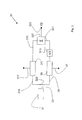
- Fig. 1 shows a block diagram of a system for generation of quadrature modulation formats
- Fig. 2 is a visualization of optical signal runs at the first input of the first optical wavelength converter, at the second input of the second optical wavelength converter and in two branches and at the output of the system for generation of quadrature modulation formats.
- FIG. 3 shows a QAM system 30 known in the prior art.
- a system 30 typically comprises a light source 31 connected to the input of a beam splitter 325 which further comprises a first output 319 connected to an input of a first electro-optical modulator 311 and a second output 35 of the beam splitter 325 connected to an input of a second electro-optical modulator 39.
- the first electro-optical modulator 311 comprises a further input 317 to which a first electrical data signal can be connected.
- the second electro-optical modulator 39 comprises a further input 37 on which a second electrical data signal can be connected.
- the output of the second electro-optical modulator 39 is connected to a phase shifter 313.
- the output of the phase shifter 313 and the output of the first electro-optical modulator 311 are connected to an adder 327.
- the light source 31 emits a light beam 33.
- This light beam 33 also referred to as optical carrier, is split such that some of the light goes into a first branch 315 or I-arm (for "inphase”-arm) and some of the light goes into a second branch 321 or Q-arm (for "quadrature”-arm).
- a first electrical data signal is fed into the first electro-optical modulator 311 via the further input 317 and a second electrical data signal is fed into the second electro-optical modulator 39 via the further input 37.
- Electro-optical modulators are modulators that have as a property that, using an electro-optical effect, an electrical signal can induce changes in the properties of the material from which the modulator is built, thus inducing changes in (or "modulating") amplitude or phase of light that is fed into the modulator.
- the first electrical data signal and the second electrical data signal each modulate individually respectively the light of the optical carrier in the first branch 315 forming a first optical signal and the light of the optical carrier in the second branch 321 forming a second optical signal.
- the second optical signal passes subsequently through the phase shifter 313, which causes the second optical signal to be delayed of ⁇ /2 the carrier wavelength.
- the first optical signal and the second optical signal are summed up in the adder 327.
- a QAM output signal 323 consisting of two modulated signals, a quadrature and an inphase one, is generated.
- the QAM output signal 323 generated in this way is then transmitted in a transmission system and received at a receiver.
- Shown in fig. 1 is an example embodiment of method for generation of advanced quadrature modulation formats, according to the invention.
- a monochromatic non-modulated continuous optical signal with a constant optical power and an output wavelength ⁇ 0 is generated in a light source 3.
- This monochromatic non-modulated continuous optical signal with a constant optical power and an output wavelength A 0 generated in the light source 3 is distributed uniformly to the second input of the first optical wavelength converter 4 and to the first input of the second optical wavelength converter 5 .
- the invention will work with any coherent light source (such as a laser) or even with a light emitting diode (“LED").
- the light source does not need to emit light in a continuous fashion, for instance a pulsed light source will work as well.
- the optical output power of the light source need not be constant.
- the distribution of the optical signal to the first and second outputs need not be uniform.
- a distribution that is non-uniform (for instance a distribution in which 55 % of the output power goes to the second input of the first optical wavelength converter 4 and in which the remaining 45 % goes to the first input of the second optical wavelength converter 5) will work as well.
- each received input optical signal is given a different amplitude
- each received input optical signal is given a different amplitude
- each received input optical signal is given a different amplitude.
- Such amplitude differentiation provides a clear identification of each received input optical signal.
- At the output of the first multi-input interface 1 appears an i-th input amplitude modulated optical signal I i (t) with a carrier having a wavelength ⁇ I
- at the output of the second multi-input interface 2 appears an i-th input amplitude modulated optical signal Q i (t) with a carrier having a wavelength ⁇ Q .
- Optical signals are transmitted from the output of each optical attenuator 1 1 , 1 2 , ... , 1 n of the first multi-input interface 1 , to the first input of the first optical wavelength converter 4 , and optical signals are transmitted from the output of each optical attenuator 2 1 , 2 2 , ... , 2 n of the second multi-input interface 2 to the second input of the second optical wavelength converter 5 .
- phase of the quadrature component Q (t) is shifted by ⁇ /2 in the domain of the output wavelength ⁇ o .
- the optical signals appearing at the output of the first optical wavelength converter 4 and at the output of the optical phase-shifter 6 are summed in the adder 7 .
- a quadraturely modulated optical signal IQ(t) with the carrier having the output wavelength ⁇ o is obtained.
- the quadrature optical signal generated in this way is transmitted in the opto-telecommunication systems with high throughputs per second.
- the first multi-input interface 1 includes n optical attenuators 1 1 , 1 2 , ..., 1 n and the second multi-input interface 2 includes n optical attenuators 2 1 , 2 2 , ..., 2 n .
- the outputs of the optical attenuators 1 1 , 1 2 , ..., 1 n of the first multi-input interface 1 are connected to the first input of the first optical wavelength converter 4
- the output of the optical attenuators 2 1 , 2 2 , ..., 2 n of the second multi-input interface 2 are connected to the second input of the second optical wavelength converter 5 .
- the output of the first optical wavelength converter 4 is connected to the first input of the adder 7 , and the output of the second optical wavelength converter 5 is connected through the optical phase-shifter 6 to the second input of the adder 7 .
- the first output of the light source 3 is connected to the second input of the first optical wavelength converter 4 , while its second output is connected to the first input of the second optical wavelength converter 5 .
- the output of the adder 7 is the output of the system 8 .
- Fig. 2 shows the signals as can be measured at several points indicated in the system shown in fig. 1 . It should be noted that the scale of the graph at the bottom of fig. 2 is different from that of the other graphs shown in fig. 2 .
- IQ (t) is the sum of I(t) and Q(t).
- Saturable absorbers or semiconductor optical amplifiers can be used as optical wavelength converters. These are optical components showing a non linear behavior of the absorption as a function of the optical input power.
- Method and system for the generation of advanced quadrature modulation formats according to the invention is suitable for use in opto-telecommunication systems for the simultaneous transmission of optical signals having different wavelengths, with high throughputs per second.
- the system shown in fig. 1 can be scaled up to generate so called higher order QAM formats such as 16 QAM.
- further optical wavelength converters each connected to a further phase shifter would be needed to receive further optical signals to modulate the light beam from the light source 3.
- These optical wavelength converters and their respective phase shifters would need to be connected in parallel with the second optical wavelength converter 5 and the optical phase-shifter 6.
Landscapes
- Physics & Mathematics (AREA)
- Electromagnetism (AREA)
- Engineering & Computer Science (AREA)
- Computer Networks & Wireless Communication (AREA)
- Signal Processing (AREA)
- Optical Communication System (AREA)
Abstract
Description
- The invention relates to a method for generation of advanced modulation formats and a system for generation of advanced modulation formats, which are particularly used in opto-communication systems with high capacities and throughput per second. An example of an advanced modulation format is Quadrature Amplitude Modulation or, in abbreviated form, "QAM".
- Methods and systems for generation of QAM formats are currently known. These systems comprise electro-optical modulators and are based on an electro-optical effect. This means that electrical signals are used to drive the modulators. Examples of such modulators are monolithic InP 16 QAM modulators and quad-parallel Mach-Zehnder modulators. The maximum bit rate of the former is typically 43 Gbit/s while the bit rate of the latter is typically limited to 50Gbit/s. These modulators consist of one or more photonic integrated circuits ("PICs"), tiny devices that integrate optical and electronic functionality. However, due to material properties, device design and other constructional constraints, the electrical bandwidth of PICs is limited and, as a consequence, so is the bandwidth of known QAM systems.
- Moreover, electrical crosstalk can lower the performance of known QAM systems because PICs, due to their small size, are quite prone to electrical interference. Besides, and despite miniaturization efforts, the known QAM systems still take up much space. They further require the input of a lot of energy to drive them.
-
EP 1076430 Al andU.S. 2008/0080859 A1 , disclose methods and systems in which the optical signal phase in one of the streams is changed in a phase-shifter. - It is an aim of the invention to provide a device for generating QAM formats at a higher bitrate, which suffers less from crosstalk problems, is more compact and operates in a more energy and environmentally friendly way. Or a device which has at least some of the aforementioned properties.
- The method for generation of quadrature modulation formats according to the invention comprises the following steps: in two multi-input interfaces each received input optical signal is given a different amplitude, and then they are transmitted to two optical wavelength converters. In a light source a monochromatic non-modulated continuous optical signal having a constant optical power and an output wavelength is generated. This signal is uniformly distributed to the second input of the first optical wavelength converter and to the first input of the second optical wavelength converter.
- In the first optical wavelength converter, optical signals from the first multi-input interface are copied concurrently onto the optical signal with the carrier having an output wavelength, and the inphase component is generated, while, in the second optical wavelength converter, optical signals from the second multi-input interface are copied concurrently onto the optical signal with the carrier having an output wavelength, and the quadrature component is generated. Subsequently, in the optical phase-shifter, the phase of the quadrature component is shifted by a Π/2 in the domain of the output wavelength.
- The optical signals appearing at the output of the first optical wavelength converter and at the output of the optical phase-shifter are added up in an adder, thus obtaining at the output of the adder, a quadraturely modulated optical signal with the carrier having an output wavelength.
- The system for generation of quadrature modulation formats according to the invention comprises the following features: the first multi-input interface includes n optical attenuators whose outputs are connected to the first input of the first optical wavelength converter, and the second multi-input interface includes n optical attenuators whose outputs are connected to the second input of the second optical wavelength converter.
- The first output of the light source is connected to the second input of the first optical wavelength converter, and the second output of the light source is connected to the first input of the second optical wavelength converter.
- The output of the first optical wavelength converter is connected to the first input of the adder, and the output of the second optical wavelength converter is connected through the optical phase shifter to the second input of the adder. The output of the adder is the output of the system.
- Advantageous effects of the method and system for generation of quadrature modulation formats according to the invention, in relation to the present state of the art, consist in the optical-only processing of optical signals, while this optical processing is carried out at higher speeds, with limited energy consumption, and with a limited impact of electronic crosstalks.
- The invention also relates to a device for generation of quadrature modulation formats comprising a light source, said light source being arranged, when said device is in operation, to output a light beam which is split in a first part and at least a second part, said device comprising at least one phase shifter for imparting a phase difference of Π/2 modulo Π to said first part with respect to said second part, characterized in that said device comprises a first optical wavelength converter being arranged to receive at least a first optical signal for modulating said first part and at least one second optical wavelength converter being arranged to receive at least a second optical signal for modulating said second part.
- Such a device has as advantages that, because the electro-optical modulators are no longer there, it contains less electronics. The major part of the operations is carried out optically, so an important reduction in electrical interference is realized. A further advantage is that the device enables to go to bit rates that are higher than those currently possible.
- In an embodiment of the invention, said first optical wavelength converter is arranged to receive at least a third optical signal for modulating said first part.
- In another embodiment of the invention, said third optical signal is attenuated before being received by said first optical wavelength converter.
- This has as an advantage that it is possible to distinguish the first and third optical signals from each other by tuning their respective amplitude.
- In another embodiment of the invention, said second optical wavelength converter is arranged to receive at least a fourth optical signal for modulating said second part.
- In another embodiment of the invention, said fourth optical signal is attenuated before being received by said second optical wavelength converter.
- In another embodiment of the invention, at least one of said first optical wavelength converter and said second optical wavelength converter is one of a saturable absorber or a semiconductor optical amplifier.
- In another embodiment of the invention, said first optical wavelength converter comprises a first output and said second optical wavelength converter comprises a second output and said first output and said second output are fed into an adder.
- The invention also relates to an optical transmission system comprising a device as described above.
- The invention also relates to a method for generation of quadrature modulation formats comprising the following steps:
- splitting a light beam output by a light source, in a first part and at least a second part,
- imparting by at least one phase shifter a phase difference of Π/2 modulo Π to said first part with respect to said second part, characterized by
- receiving by a first optical wavelength converter at least a first optical signal for modulating said first part and
- receiving by at least a second optical wavelength converter at least a second optical signal for modulating said second part.
- The invention also relates to a computer program comprising program code means for performing all the steps described above when said program is run on a computer.
- The invention also relates to a computer program product comprising program code means stored on a computer readable medium for performing the method described above when said program product is run on a computer.
- The invention will be explained in further detail, and by way of example, with reference to the accompanying drawings in which
Fig. 3 shows a QAM system as currently known,
Fig. 1 shows a block diagram of a system for generation of quadrature modulation formats, and
Fig. 2 is a visualization of optical signal runs at the first input of the first optical wavelength converter, at the second input of the second optical wavelength converter and in two branches and at the output of the system for generation of quadrature modulation formats. -
Figure 3 shows aQAM system 30 known in the prior art. Such asystem 30 typically comprises alight source 31 connected to the input of abeam splitter 325 which further comprises afirst output 319 connected to an input of a first electro-optical modulator 311 and asecond output 35 of thebeam splitter 325 connected to an input of a second electro-optical modulator 39. The first electro-optical modulator 311 comprises afurther input 317 to which a first electrical data signal can be connected. On its turn, and in a comparable way, the second electro-optical modulator 39 comprises afurther input 37 on which a second electrical data signal can be connected. The output of the second electro-optical modulator 39 is connected to aphase shifter 313. The output of thephase shifter 313 and the output of the first electro-optical modulator 311 are connected to anadder 327. - In operation of the
system 30, thelight source 31 emits alight beam 33. Thislight beam 33, also referred to as optical carrier, is split such that some of the light goes into afirst branch 315 or I-arm (for "inphase"-arm) and some of the light goes into asecond branch 321 or Q-arm (for "quadrature"-arm). A first electrical data signal is fed into the first electro-optical modulator 311 via thefurther input 317 and a second electrical data signal is fed into the second electro-optical modulator 39 via thefurther input 37. - Electro-optical modulators, as will be appreciated by a person skilled in the arts, are modulators that have as a property that, using an electro-optical effect, an electrical signal can induce changes in the properties of the material from which the modulator is built, thus inducing changes in (or "modulating") amplitude or phase of light that is fed into the modulator.
- Thus, in the system shown in
figure 3 , the first electrical data signal and the second electrical data signal each modulate individually respectively the light of the optical carrier in thefirst branch 315 forming a first optical signal and the light of the optical carrier in thesecond branch 321 forming a second optical signal. The second optical signal passes subsequently through thephase shifter 313, which causes the second optical signal to be delayed of Π/2 the carrier wavelength. Finally the first optical signal and the second optical signal are summed up in theadder 327. In this way, aQAM output signal 323 consisting of two modulated signals, a quadrature and an inphase one, is generated. TheQAM output signal 323 generated in this way is then transmitted in a transmission system and received at a receiver. - Shown in
fig. 1 is an example embodiment of method for generation of advanced quadrature modulation formats, according to the invention. A monochromatic non-modulated continuous optical signal with a constant optical power and an output wavelength λ 0 is generated in alight source 3. This monochromatic non-modulated continuous optical signal with a constant optical power and an output wavelength A 0 generated in the light source 3is distributed uniformly to the second input of the firstoptical wavelength converter 4 and to the first input of the second optical wavelength converter 5.It should however be noted that the invention will work with any coherent light source (such as a laser) or even with a light emitting diode ("LED"). In addition, the light source does not need to emit light in a continuous fashion, for instance a pulsed light source will work as well. Nor need the optical output power of the light source be constant. Also, the distribution of the optical signal to the first and second outputs need not be uniform. A distribution that is non-uniform (for instance a distribution in which 55 % of the output power goes to the second input of the firstoptical wavelength converter 4 and in which the remaining 45 % goes to the first input of the second optical wavelength converter 5) will work as well. - In the first
multi-input interface 1 each received input optical signal is given a different amplitude, and in the secondmulti-input interface 2 each received input optical signal is given a different amplitude. Such amplitude differentiation provides a clear identification of each received input optical signal. At the output of the first multi-input interface 1appears an i-th input amplitude modulated optical signal I i (t) with a carrier having a wavelength λ I , while at the output of the secondmulti-input interface 2 appears an i-th input amplitude modulated optical signal Q i (t) with a carrier having a wavelength λ Q . - Optical signals are transmitted from the output of each
optical attenuator multi-input interface 1, to the first input of the firstoptical wavelength converter 4, and optical signals are transmitted from the output of eachoptical attenuator multi-input interface 2 to the second input of the secondoptical wavelength converter 5. - In the first
optical wavelength converter 4, optical signals I i (t) , where i = 1, 2, ... , n, are copied from the firstmulti-input interface 1 onto the optical signal with the output carrier having a wavelength λ o , and a inphase component I (t) is generated, while in the secondoptical wavelength converter 5 optical signals Q i (t), where i = 1, 2, ... n, are copied from the secondmulti-input interface 2 onto the optical signal with the output carrier having a wavelength λ o , and a quadrature component Q(t) is_generated. - Next, in the optical phase-
shifter 6 the phase of the quadrature component Q (t) is shifted by Π/2 in the domain of the output wavelength λ o . - The optical signals appearing at the output of the first
optical wavelength converter 4 and at the output of the optical phase-shifter 6 are summed in theadder 7. At the output of theadder 7, a quadraturely modulated optical signal IQ(t) with the carrier having the output wavelength λ o is obtained. The quadrature optical signal generated in this way is transmitted in the opto-telecommunication systems with high throughputs per second. - In the example embodiment of a system for generation of advanced quadrature modulation formats according to the invention, the first
multi-input interface 1 includes noptical attenuators multi-input interface 2 includes noptical attenuators optical attenuators multi-input interface 1 are connected to the first input of the firstoptical wavelength converter 4, and the output of theoptical attenuators multi-input interface 2 are connected to the second input of the secondoptical wavelength converter 5. - The output of the first
optical wavelength converter 4 is connected to the first input of theadder 7, and the output of the secondoptical wavelength converter 5 is connected through the optical phase-shifter 6 to the second input of theadder 7. The first output of thelight source 3 is connected to the second input of the firstoptical wavelength converter 4, while its second output is connected to the first input of the secondoptical wavelength converter 5. The output of theadder 7 is the output of the system 8. -
Fig. 2 shows the signals as can be measured at several points indicated in the system shown infig. 1 . It should be noted that the scale of the graph at the bottom offig. 2 is different from that of the other graphs shown infig. 2 . IQ (t) is the sum of I(t) and Q(t). - Saturable absorbers or semiconductor optical amplifiers can be used as optical wavelength converters. These are optical components showing a non linear behavior of the absorption as a function of the optical input power.
- Method and system for the generation of advanced quadrature modulation formats according to the invention is suitable for use in opto-telecommunication systems for the simultaneous transmission of optical signals having different wavelengths, with high throughputs per second.
- Although method and system for the generation of quadrature modulation formats according to the invention is disclosed in the patent claims, as well as presented in the form of a specific example embodiment in the description of the invention, and depicted on the drawing, for one skilled in the art of optical signal processing in opto-telecommunication systems it is obvious that the data contained therein concerning method and system for the generation of advanced quadrature modulation formats cannot be interpreted as restricting the inventive idea only to these data.
- It should for example be noted that the system shown in
fig. 1 can be scaled up to generate so called higher order QAM formats such as 16 QAM. In such a case further optical wavelength converters each connected to a further phase shifter would be needed to receive further optical signals to modulate the light beam from thelight source 3. These optical wavelength converters and their respective phase shifters would need to be connected in parallel with the secondoptical wavelength converter 5 and the optical phase-shifter 6.
Claims (13)
- Method for generation of quadrature modulation formats, in which input modulated optical signals are fed to a first interface and a second interface, and then in one of these input modulated optical signals the phase is shifted, and then input modulated optical signals are subject to summation in one of these transformed input optical signals the phase is shifted, and then the transformed optical signals are subjected to summation, characterized in that in multi-input interfaces (1, 2) each received input optical signal is given a different amplitude, and then they are transmitted to optical wavelength converters (4, 5), in a light source (3) a monochromatic non-modulated continuous optical signal having a constant optical power and an output wavelength (λ o ) is generated, this optical signal is being uniformly distributed to the second input of the first optical wavelength converter (4) and to the first input of the second optical wavelength converter (5), and in the first optical wavelength converter (4) the optical signals from the first multi-input interface (1) are simultaneously copied into the optical signal with the carrier having an output wavelength (λ o ), and a inphase component (I(t)) is generated, whereas in the second optical wavelength converter (5) the optical signals from the second multi-input interface (2) are simultaneously copied onto the optical signal with the carrier having an output wavelength (λ o ), and a quadrature component (Q(t)) is generated, and then the phase of the quadrature component (Q(t)), in the optical phase-shifter (6), is shifted by Π/2 in the domain of the output wavelength (λ o ), where after the optical signals appearing at the output of the first optical wavelength converter (4) and at the output of the optical phase-shifter (6), are summed up in the adder (7), and, on its output, a quadraturely modulated optical signal (IQ(t)) with the carrier having an output wavelength (λ o ) is obtained.
- System for generation of quadrature modulation formats with two multi-input interfaces of modulated optical signals comprising an optical phase-shifter, an adder an a light source, characterized in that the first multi-input interface (1) includes n optical attenuators (11, 12, ... , 1n) whose outputs are connected to the first input of the first optical wavelength converter (4), and the second multi-input interface (2) includes n optical attenuators (21, 22, ..., 2n) whose outputs are connected to the second input of the second optical wavelength converter (5), the output of the first optical wavelength converter (4) being connected to the first input of the adder (7)and the output of the second optical wavelength converter (5) (6) being connected through the optical phase-shifter to the second input of the adder (7), and the first output of the light source (3) is connected to the second input of the first optical wavelength converter (4) while its second output is connected to the first input of the second optical wavelength converter (5), and the output of the adder (7) is the output of the system (8).
- Device for generation of quadrature modulation formats comprising a light source (3), said light source (3) being arranged, when said device is in operation, to output a light beam which is split in a first part and at least a second part, said device comprising at least one phase shifter (6) for imparting a phase difference of Π/2 modulo Π to said first part with respect to said second part,
characterized in that
said device comprises a first optical wavelength converter (4) being arranged to receive at least a first optical signal for modulating said first part and at least one second optical wavelength converter (5) being arranged to receive at least a second optical signal for modulating said second part. - Device according to claim 3 wherein said first optical wavelength converter (4) is arranged to receive at least a third optical signal for modulating said first part.
- Device according to claim 4 wherein said third optical signal is attenuated before being received by said first optical wavelength converter (4).
- Device according to anyone of the claims 3 to 5 wherein said second optical wavelength converter (5) is arranged to receive at least a fourth optical signal for modulating said second part.
- Device according to claim 6 wherein said fourth optical signal is attenuated before being received by said second optical wavelength converter (5).
- Device according to any of the claims 1 to 7 wherein at least one of said first optical wavelength converter (4) and said second optical wavelength converter (5) is one of a saturable absorber or a semiconductor optical amplifier.
- Device according to any of the claims 3 to 8 wherein said first optical wavelength converter (4) comprises a first output and said second optical wavelength converter (5) comprises a second output and said first output and said second output are fed into an adder (7).
- Optical transmission system comprising a device according to any of the claims 1 to 9.
- Method for generation of quadrature modulation formats comprising the following steps:- splitting a light beam output by a light source (3), in a first part and at least a second part,- imparting by at least one phase shifter (6) a phase difference of Π/2 modulo Π to said first part with respect to said second part,characterized by- receiving by a first optical wavelength converter (4) at least a first optical signal for modulating said first part and- receiving by at least a second optical wavelength converter (5) at least a second optical signal for modulating said second part.
- A computer program comprising program code means for performing all the steps of claim 11 when said program is run on a computer.
- A computer program product comprising program code means stored on a computer readable medium for performing the method according to claim 11 when said program product is run on a computer.
Priority Applications (1)
| Application Number | Priority Date | Filing Date | Title |
|---|---|---|---|
| EP10305702.2A EP2403163B1 (en) | 2010-06-29 | 2010-06-29 | Method and system for generation of QAM formats for applications in optical communication |
Applications Claiming Priority (1)
| Application Number | Priority Date | Filing Date | Title |
|---|---|---|---|
| EP10305702.2A EP2403163B1 (en) | 2010-06-29 | 2010-06-29 | Method and system for generation of QAM formats for applications in optical communication |
Publications (2)
| Publication Number | Publication Date |
|---|---|
| EP2403163A1 true EP2403163A1 (en) | 2012-01-04 |
| EP2403163B1 EP2403163B1 (en) | 2016-12-28 |
Family
ID=43127144
Family Applications (1)
| Application Number | Title | Priority Date | Filing Date |
|---|---|---|---|
| EP10305702.2A Active EP2403163B1 (en) | 2010-06-29 | 2010-06-29 | Method and system for generation of QAM formats for applications in optical communication |
Country Status (1)
| Country | Link |
|---|---|
| EP (1) | EP2403163B1 (en) |
Citations (6)
| Publication number | Priority date | Publication date | Assignee | Title |
|---|---|---|---|---|
| EP1076430A1 (en) | 1999-07-23 | 2001-02-14 | BRITISH TELECOMMUNICATIONS public limited company | Optical regenerator for high-bitrate OTDM signals |
| EP1184715A1 (en) * | 2000-07-07 | 2002-03-06 | Lucent Technologies Inc. | Optical wavelength converter |
| US20080080859A1 (en) | 2006-09-28 | 2008-04-03 | Oki Electric Industry Co., Ltd. | OTDM-DPSK signal generator capable of detecting an optical carrier phase difference between optical pulses |
| US20080297270A1 (en) * | 2006-02-03 | 2008-12-04 | Tomoo Takahara | Driver circuit of optical modulator |
| WO2009012419A2 (en) * | 2007-07-17 | 2009-01-22 | Opvista Incorporated | Optical wavelength-division-multiplexed (wdm) comb generator using a single laser |
| EP2166681A1 (en) * | 2007-07-06 | 2010-03-24 | Nippon Telegraph and Telephone Corporation | Optical modulation circuit and optical transmission system |
-
2010
- 2010-06-29 EP EP10305702.2A patent/EP2403163B1/en active Active
Patent Citations (6)
| Publication number | Priority date | Publication date | Assignee | Title |
|---|---|---|---|---|
| EP1076430A1 (en) | 1999-07-23 | 2001-02-14 | BRITISH TELECOMMUNICATIONS public limited company | Optical regenerator for high-bitrate OTDM signals |
| EP1184715A1 (en) * | 2000-07-07 | 2002-03-06 | Lucent Technologies Inc. | Optical wavelength converter |
| US20080297270A1 (en) * | 2006-02-03 | 2008-12-04 | Tomoo Takahara | Driver circuit of optical modulator |
| US20080080859A1 (en) | 2006-09-28 | 2008-04-03 | Oki Electric Industry Co., Ltd. | OTDM-DPSK signal generator capable of detecting an optical carrier phase difference between optical pulses |
| EP2166681A1 (en) * | 2007-07-06 | 2010-03-24 | Nippon Telegraph and Telephone Corporation | Optical modulation circuit and optical transmission system |
| WO2009012419A2 (en) * | 2007-07-17 | 2009-01-22 | Opvista Incorporated | Optical wavelength-division-multiplexed (wdm) comb generator using a single laser |
Also Published As
| Publication number | Publication date |
|---|---|
| EP2403163B1 (en) | 2016-12-28 |
Similar Documents
| Publication | Publication Date | Title |
|---|---|---|
| CN101634759B (en) | Method for controlling photomodulator bias voltage and relevant device | |
| US20040021829A1 (en) | Multi-level optical signal generation | |
| US9312962B2 (en) | Intensity-based modulator | |
| US20100021182A1 (en) | Optical transmitter | |
| US20140133870A1 (en) | Optical transmitter for generating multi-level optical signal and method therefor | |
| CN113541806A (en) | 16 frequency multiplication millimeter wave signal generation device and method based on parallel Mach-Zehnder modulator | |
| US10763637B2 (en) | Optical signal generation device and method and chip | |
| US9337936B2 (en) | Optical transmission apparatus, optical transmission method and program for optical transmission | |
| US20110052209A1 (en) | High-Speed Multi-Level Electronic Signal Generation for Optical Communications | |
| US10234704B2 (en) | Optical module that includes optical modulator and bias control method for optical modulator | |
| US7146109B2 (en) | Analog modulation of optical signals | |
| CN102204201B (en) | Method and apparatus for compatibly realizing pdm-bpsk and qpsk modulation | |
| CN102469378B (en) | Optical communication system and method and reflective optical network device thereof | |
| JP6456489B2 (en) | Dummy light generation device, optical transmission device, and dummy light generation method | |
| Li et al. | Photonic generation of dual-band microwave waveforms with simultaneous and diverse modulation formats | |
| EP2908449A1 (en) | Device for transmitting and/or modulating optical signals with passive phase shifters | |
| CA2575595C (en) | Multiple wavelength light source, and generation method for multiple wavelength light | |
| CN114614907B (en) | Microwave waveform compiling method based on optical domain inverse Fourier transform | |
| EP2403163B1 (en) | Method and system for generation of QAM formats for applications in optical communication | |
| Wang et al. | Photonic generation of microwave binary modulation signals with high frequency multiplication factors | |
| Chan et al. | All-optical frequency shifter based on stimulated Brillouin scattering in an optical fiber | |
| JP6191595B2 (en) | Optical communication system, optical transmission apparatus, optical communication method, and optical transmission method | |
| Stephanie et al. | Photonic neuron with on Frequency-Domain ReLU activation function | |
| CN112783260A (en) | Optical computing device, optical computing method and computing system | |
| CN113141213B (en) | Coherent transmitter, method for controlling coherent transmitter and coherent transceiving system |
Legal Events
| Date | Code | Title | Description |
|---|---|---|---|
| AK | Designated contracting states |
Kind code of ref document: A1 Designated state(s): AL AT BE BG CH CY CZ DE DK EE ES FI FR GB GR HR HU IE IS IT LI LT LU LV MC MK MT NL NO PL PT RO SE SI SK SM TR |
|
| AX | Request for extension of the european patent |
Extension state: BA ME RS |
|
| PUAI | Public reference made under article 153(3) epc to a published international application that has entered the european phase |
Free format text: ORIGINAL CODE: 0009012 |
|
| 17P | Request for examination filed |
Effective date: 20120613 |
|
| RAP1 | Party data changed (applicant data changed or rights of an application transferred) |
Owner name: ORANGE |
|
| REG | Reference to a national code |
Ref country code: DE Ref legal event code: R079 Ref document number: 602010039118 Country of ref document: DE Free format text: PREVIOUS MAIN CLASS: H04B0010040000 Ipc: H04B0010500000 |
|
| GRAP | Despatch of communication of intention to grant a patent |
Free format text: ORIGINAL CODE: EPIDOSNIGR1 |
|
| RIC1 | Information provided on ipc code assigned before grant |
Ipc: H04B 10/516 20130101ALI20160622BHEP Ipc: H04B 10/50 20130101AFI20160622BHEP |
|
| INTG | Intention to grant announced |
Effective date: 20160725 |
|
| GRAS | Grant fee paid |
Free format text: ORIGINAL CODE: EPIDOSNIGR3 |
|
| GRAA | (expected) grant |
Free format text: ORIGINAL CODE: 0009210 |
|
| AK | Designated contracting states |
Kind code of ref document: B1 Designated state(s): AL AT BE BG CH CY CZ DE DK EE ES FI FR GB GR HR HU IE IS IT LI LT LU LV MC MK MT NL NO PL PT RO SE SI SK SM TR |
|
| REG | Reference to a national code |
Ref country code: GB Ref legal event code: FG4D |
|
| REG | Reference to a national code |
Ref country code: CH Ref legal event code: EP |
|
| REG | Reference to a national code |
Ref country code: AT Ref legal event code: REF Ref document number: 858092 Country of ref document: AT Kind code of ref document: T Effective date: 20170115 |
|
| REG | Reference to a national code |
Ref country code: IE Ref legal event code: FG4D |
|
| REG | Reference to a national code |
Ref country code: DE Ref legal event code: R096 Ref document number: 602010039118 Country of ref document: DE |
|
| PG25 | Lapsed in a contracting state [announced via postgrant information from national office to epo] |
Ref country code: LV Free format text: LAPSE BECAUSE OF FAILURE TO SUBMIT A TRANSLATION OF THE DESCRIPTION OR TO PAY THE FEE WITHIN THE PRESCRIBED TIME-LIMIT Effective date: 20161228 |
|
| REG | Reference to a national code |
Ref country code: LT Ref legal event code: MG4D |
|
| PG25 | Lapsed in a contracting state [announced via postgrant information from national office to epo] |
Ref country code: LT Free format text: LAPSE BECAUSE OF FAILURE TO SUBMIT A TRANSLATION OF THE DESCRIPTION OR TO PAY THE FEE WITHIN THE PRESCRIBED TIME-LIMIT Effective date: 20161228 Ref country code: GR Free format text: LAPSE BECAUSE OF FAILURE TO SUBMIT A TRANSLATION OF THE DESCRIPTION OR TO PAY THE FEE WITHIN THE PRESCRIBED TIME-LIMIT Effective date: 20170329 Ref country code: NO Free format text: LAPSE BECAUSE OF FAILURE TO SUBMIT A TRANSLATION OF THE DESCRIPTION OR TO PAY THE FEE WITHIN THE PRESCRIBED TIME-LIMIT Effective date: 20170328 Ref country code: SE Free format text: LAPSE BECAUSE OF FAILURE TO SUBMIT A TRANSLATION OF THE DESCRIPTION OR TO PAY THE FEE WITHIN THE PRESCRIBED TIME-LIMIT Effective date: 20161228 |
|
| REG | Reference to a national code |
Ref country code: NL Ref legal event code: MP Effective date: 20161228 |
|
| REG | Reference to a national code |
Ref country code: AT Ref legal event code: MK05 Ref document number: 858092 Country of ref document: AT Kind code of ref document: T Effective date: 20161228 |
|
| REG | Reference to a national code |
Ref country code: FR Ref legal event code: PLFP Year of fee payment: 8 |
|
| PG25 | Lapsed in a contracting state [announced via postgrant information from national office to epo] |
Ref country code: FI Free format text: LAPSE BECAUSE OF FAILURE TO SUBMIT A TRANSLATION OF THE DESCRIPTION OR TO PAY THE FEE WITHIN THE PRESCRIBED TIME-LIMIT Effective date: 20161228 Ref country code: HR Free format text: LAPSE BECAUSE OF FAILURE TO SUBMIT A TRANSLATION OF THE DESCRIPTION OR TO PAY THE FEE WITHIN THE PRESCRIBED TIME-LIMIT Effective date: 20161228 |
|
| PG25 | Lapsed in a contracting state [announced via postgrant information from national office to epo] |
Ref country code: NL Free format text: LAPSE BECAUSE OF FAILURE TO SUBMIT A TRANSLATION OF THE DESCRIPTION OR TO PAY THE FEE WITHIN THE PRESCRIBED TIME-LIMIT Effective date: 20161228 |
|
| PG25 | Lapsed in a contracting state [announced via postgrant information from national office to epo] |
Ref country code: RO Free format text: LAPSE BECAUSE OF FAILURE TO SUBMIT A TRANSLATION OF THE DESCRIPTION OR TO PAY THE FEE WITHIN THE PRESCRIBED TIME-LIMIT Effective date: 20161228 Ref country code: CZ Free format text: LAPSE BECAUSE OF FAILURE TO SUBMIT A TRANSLATION OF THE DESCRIPTION OR TO PAY THE FEE WITHIN THE PRESCRIBED TIME-LIMIT Effective date: 20161228 Ref country code: EE Free format text: LAPSE BECAUSE OF FAILURE TO SUBMIT A TRANSLATION OF THE DESCRIPTION OR TO PAY THE FEE WITHIN THE PRESCRIBED TIME-LIMIT Effective date: 20161228 Ref country code: SK Free format text: LAPSE BECAUSE OF FAILURE TO SUBMIT A TRANSLATION OF THE DESCRIPTION OR TO PAY THE FEE WITHIN THE PRESCRIBED TIME-LIMIT Effective date: 20161228 Ref country code: IS Free format text: LAPSE BECAUSE OF FAILURE TO SUBMIT A TRANSLATION OF THE DESCRIPTION OR TO PAY THE FEE WITHIN THE PRESCRIBED TIME-LIMIT Effective date: 20170428 |
|
| PG25 | Lapsed in a contracting state [announced via postgrant information from national office to epo] |
Ref country code: IT Free format text: LAPSE BECAUSE OF FAILURE TO SUBMIT A TRANSLATION OF THE DESCRIPTION OR TO PAY THE FEE WITHIN THE PRESCRIBED TIME-LIMIT Effective date: 20161228 Ref country code: SM Free format text: LAPSE BECAUSE OF FAILURE TO SUBMIT A TRANSLATION OF THE DESCRIPTION OR TO PAY THE FEE WITHIN THE PRESCRIBED TIME-LIMIT Effective date: 20161228 Ref country code: BG Free format text: LAPSE BECAUSE OF FAILURE TO SUBMIT A TRANSLATION OF THE DESCRIPTION OR TO PAY THE FEE WITHIN THE PRESCRIBED TIME-LIMIT Effective date: 20170328 Ref country code: ES Free format text: LAPSE BECAUSE OF FAILURE TO SUBMIT A TRANSLATION OF THE DESCRIPTION OR TO PAY THE FEE WITHIN THE PRESCRIBED TIME-LIMIT Effective date: 20161228 Ref country code: AT Free format text: LAPSE BECAUSE OF FAILURE TO SUBMIT A TRANSLATION OF THE DESCRIPTION OR TO PAY THE FEE WITHIN THE PRESCRIBED TIME-LIMIT Effective date: 20161228 Ref country code: PL Free format text: LAPSE BECAUSE OF FAILURE TO SUBMIT A TRANSLATION OF THE DESCRIPTION OR TO PAY THE FEE WITHIN THE PRESCRIBED TIME-LIMIT Effective date: 20161228 Ref country code: BE Free format text: LAPSE BECAUSE OF FAILURE TO SUBMIT A TRANSLATION OF THE DESCRIPTION OR TO PAY THE FEE WITHIN THE PRESCRIBED TIME-LIMIT Effective date: 20161228 Ref country code: PT Free format text: LAPSE BECAUSE OF FAILURE TO SUBMIT A TRANSLATION OF THE DESCRIPTION OR TO PAY THE FEE WITHIN THE PRESCRIBED TIME-LIMIT Effective date: 20170428 |
|
| REG | Reference to a national code |
Ref country code: DE Ref legal event code: R097 Ref document number: 602010039118 Country of ref document: DE |
|
| PLBE | No opposition filed within time limit |
Free format text: ORIGINAL CODE: 0009261 |
|
| STAA | Information on the status of an ep patent application or granted ep patent |
Free format text: STATUS: NO OPPOSITION FILED WITHIN TIME LIMIT |
|
| PG25 | Lapsed in a contracting state [announced via postgrant information from national office to epo] |
Ref country code: DK Free format text: LAPSE BECAUSE OF FAILURE TO SUBMIT A TRANSLATION OF THE DESCRIPTION OR TO PAY THE FEE WITHIN THE PRESCRIBED TIME-LIMIT Effective date: 20161228 |
|
| 26N | No opposition filed |
Effective date: 20170929 |
|
| PG25 | Lapsed in a contracting state [announced via postgrant information from national office to epo] |
Ref country code: MC Free format text: LAPSE BECAUSE OF FAILURE TO SUBMIT A TRANSLATION OF THE DESCRIPTION OR TO PAY THE FEE WITHIN THE PRESCRIBED TIME-LIMIT Effective date: 20161228 |
|
| REG | Reference to a national code |
Ref country code: CH Ref legal event code: PL |
|
| PG25 | Lapsed in a contracting state [announced via postgrant information from national office to epo] |
Ref country code: SI Free format text: LAPSE BECAUSE OF FAILURE TO SUBMIT A TRANSLATION OF THE DESCRIPTION OR TO PAY THE FEE WITHIN THE PRESCRIBED TIME-LIMIT Effective date: 20161228 |
|
| REG | Reference to a national code |
Ref country code: IE Ref legal event code: MM4A |
|
| PG25 | Lapsed in a contracting state [announced via postgrant information from national office to epo] |
Ref country code: IE Free format text: LAPSE BECAUSE OF NON-PAYMENT OF DUE FEES Effective date: 20170629 Ref country code: CH Free format text: LAPSE BECAUSE OF NON-PAYMENT OF DUE FEES Effective date: 20170630 Ref country code: LI Free format text: LAPSE BECAUSE OF NON-PAYMENT OF DUE FEES Effective date: 20170630 Ref country code: LU Free format text: LAPSE BECAUSE OF NON-PAYMENT OF DUE FEES Effective date: 20170629 |
|
| REG | Reference to a national code |
Ref country code: FR Ref legal event code: PLFP Year of fee payment: 9 |
|
| PG25 | Lapsed in a contracting state [announced via postgrant information from national office to epo] |
Ref country code: MT Free format text: LAPSE BECAUSE OF NON-PAYMENT OF DUE FEES Effective date: 20170629 |
|
| PG25 | Lapsed in a contracting state [announced via postgrant information from national office to epo] |
Ref country code: HU Free format text: LAPSE BECAUSE OF FAILURE TO SUBMIT A TRANSLATION OF THE DESCRIPTION OR TO PAY THE FEE WITHIN THE PRESCRIBED TIME-LIMIT; INVALID AB INITIO Effective date: 20100629 |
|
| PG25 | Lapsed in a contracting state [announced via postgrant information from national office to epo] |
Ref country code: CY Free format text: LAPSE BECAUSE OF NON-PAYMENT OF DUE FEES Effective date: 20161228 |
|
| PG25 | Lapsed in a contracting state [announced via postgrant information from national office to epo] |
Ref country code: MK Free format text: LAPSE BECAUSE OF FAILURE TO SUBMIT A TRANSLATION OF THE DESCRIPTION OR TO PAY THE FEE WITHIN THE PRESCRIBED TIME-LIMIT Effective date: 20161228 |
|
| PG25 | Lapsed in a contracting state [announced via postgrant information from national office to epo] |
Ref country code: TR Free format text: LAPSE BECAUSE OF FAILURE TO SUBMIT A TRANSLATION OF THE DESCRIPTION OR TO PAY THE FEE WITHIN THE PRESCRIBED TIME-LIMIT Effective date: 20161228 |
|
| PG25 | Lapsed in a contracting state [announced via postgrant information from national office to epo] |
Ref country code: AL Free format text: LAPSE BECAUSE OF FAILURE TO SUBMIT A TRANSLATION OF THE DESCRIPTION OR TO PAY THE FEE WITHIN THE PRESCRIBED TIME-LIMIT Effective date: 20161228 |
|
| PGFP | Annual fee paid to national office [announced via postgrant information from national office to epo] |
Ref country code: DE Payment date: 20250520 Year of fee payment: 16 |
|
| PGFP | Annual fee paid to national office [announced via postgrant information from national office to epo] |
Ref country code: GB Payment date: 20250520 Year of fee payment: 16 |
|
| PGFP | Annual fee paid to national office [announced via postgrant information from national office to epo] |
Ref country code: FR Payment date: 20250521 Year of fee payment: 16 |