EP2403006A1 - HETERO Pn JUNCTION SEMICONDUCTOR AND PROCESS FOR PRODUCING SAME - Google Patents
HETERO Pn JUNCTION SEMICONDUCTOR AND PROCESS FOR PRODUCING SAME Download PDFInfo
- Publication number
- EP2403006A1 EP2403006A1 EP10746343A EP10746343A EP2403006A1 EP 2403006 A1 EP2403006 A1 EP 2403006A1 EP 10746343 A EP10746343 A EP 10746343A EP 10746343 A EP10746343 A EP 10746343A EP 2403006 A1 EP2403006 A1 EP 2403006A1
- Authority
- EP
- European Patent Office
- Prior art keywords
- electrically conductive
- conductive polymer
- type semiconductor
- nanoparticles
- inorganic oxide
- Prior art date
- Legal status (The legal status is an assumption and is not a legal conclusion. Google has not performed a legal analysis and makes no representation as to the accuracy of the status listed.)
- Withdrawn
Links
Images









Classifications
-
- H—ELECTRICITY
- H10—SEMICONDUCTOR DEVICES; ELECTRIC SOLID-STATE DEVICES NOT OTHERWISE PROVIDED FOR
- H10D—INORGANIC ELECTRIC SEMICONDUCTOR DEVICES
- H10D62/00—Semiconductor bodies, or regions thereof, of devices having potential barriers
- H10D62/80—Semiconductor bodies, or regions thereof, of devices having potential barriers characterised by the materials
- H10D62/81—Semiconductor bodies, or regions thereof, of devices having potential barriers characterised by the materials of structures exhibiting quantum-confinement effects, e.g. single quantum wells; of structures having periodic or quasi-periodic potential variation
-
- H—ELECTRICITY
- H10—SEMICONDUCTOR DEVICES; ELECTRIC SOLID-STATE DEVICES NOT OTHERWISE PROVIDED FOR
- H10F—INORGANIC SEMICONDUCTOR DEVICES SENSITIVE TO INFRARED RADIATION, LIGHT, ELECTROMAGNETIC RADIATION OF SHORTER WAVELENGTH OR CORPUSCULAR RADIATION
- H10F77/00—Constructional details of devices covered by this subclass
- H10F77/10—Semiconductor bodies
- H10F77/14—Shape of semiconductor bodies; Shapes, relative sizes or dispositions of semiconductor regions within semiconductor bodies
- H10F77/147—Shapes of bodies
-
- H—ELECTRICITY
- H10—SEMICONDUCTOR DEVICES; ELECTRIC SOLID-STATE DEVICES NOT OTHERWISE PROVIDED FOR
- H10K—ORGANIC ELECTRIC SOLID-STATE DEVICES
- H10K30/00—Organic devices sensitive to infrared radiation, light, electromagnetic radiation of shorter wavelength or corpuscular radiation
- H10K30/10—Organic devices sensitive to infrared radiation, light, electromagnetic radiation of shorter wavelength or corpuscular radiation comprising heterojunctions between organic semiconductors and inorganic semiconductors
- H10K30/15—Sensitised wide-bandgap semiconductor devices, e.g. dye-sensitised TiO2
-
- H—ELECTRICITY
- H10—SEMICONDUCTOR DEVICES; ELECTRIC SOLID-STATE DEVICES NOT OTHERWISE PROVIDED FOR
- H10K—ORGANIC ELECTRIC SOLID-STATE DEVICES
- H10K30/00—Organic devices sensitive to infrared radiation, light, electromagnetic radiation of shorter wavelength or corpuscular radiation
- H10K30/30—Organic devices sensitive to infrared radiation, light, electromagnetic radiation of shorter wavelength or corpuscular radiation comprising bulk heterojunctions, e.g. interpenetrating networks of donor and acceptor material domains
- H10K30/35—Organic devices sensitive to infrared radiation, light, electromagnetic radiation of shorter wavelength or corpuscular radiation comprising bulk heterojunctions, e.g. interpenetrating networks of donor and acceptor material domains comprising inorganic nanostructures, e.g. CdSe nanoparticles
-
- H—ELECTRICITY
- H10—SEMICONDUCTOR DEVICES; ELECTRIC SOLID-STATE DEVICES NOT OTHERWISE PROVIDED FOR
- H10K—ORGANIC ELECTRIC SOLID-STATE DEVICES
- H10K71/00—Manufacture or treatment specially adapted for the organic devices covered by this subclass
- H10K71/10—Deposition of organic active material
- H10K71/12—Deposition of organic active material using liquid deposition, e.g. spin coating
- H10K71/125—Deposition of organic active material using liquid deposition, e.g. spin coating using electrolytic deposition e.g. in-situ electropolymerisation
-
- H—ELECTRICITY
- H10—SEMICONDUCTOR DEVICES; ELECTRIC SOLID-STATE DEVICES NOT OTHERWISE PROVIDED FOR
- H10D—INORGANIC ELECTRIC SEMICONDUCTOR DEVICES
- H10D8/00—Diodes
-
- H—ELECTRICITY
- H10—SEMICONDUCTOR DEVICES; ELECTRIC SOLID-STATE DEVICES NOT OTHERWISE PROVIDED FOR
- H10K—ORGANIC ELECTRIC SOLID-STATE DEVICES
- H10K30/00—Organic devices sensitive to infrared radiation, light, electromagnetic radiation of shorter wavelength or corpuscular radiation
- H10K30/10—Organic devices sensitive to infrared radiation, light, electromagnetic radiation of shorter wavelength or corpuscular radiation comprising heterojunctions between organic semiconductors and inorganic semiconductors
- H10K30/15—Sensitised wide-bandgap semiconductor devices, e.g. dye-sensitised TiO2
- H10K30/151—Sensitised wide-bandgap semiconductor devices, e.g. dye-sensitised TiO2 the wide bandgap semiconductor comprising titanium oxide, e.g. TiO2
-
- H—ELECTRICITY
- H10—SEMICONDUCTOR DEVICES; ELECTRIC SOLID-STATE DEVICES NOT OTHERWISE PROVIDED FOR
- H10K—ORGANIC ELECTRIC SOLID-STATE DEVICES
- H10K30/00—Organic devices sensitive to infrared radiation, light, electromagnetic radiation of shorter wavelength or corpuscular radiation
- H10K30/50—Photovoltaic [PV] devices
-
- H—ELECTRICITY
- H10—SEMICONDUCTOR DEVICES; ELECTRIC SOLID-STATE DEVICES NOT OTHERWISE PROVIDED FOR
- H10K—ORGANIC ELECTRIC SOLID-STATE DEVICES
- H10K85/00—Organic materials used in the body or electrodes of devices covered by this subclass
- H10K85/10—Organic polymers or oligomers
- H10K85/111—Organic polymers or oligomers comprising aromatic, heteroaromatic, or aryl chains, e.g. polyaniline, polyphenylene or polyphenylene vinylene
- H10K85/113—Heteroaromatic compounds comprising sulfur or selene, e.g. polythiophene
-
- Y—GENERAL TAGGING OF NEW TECHNOLOGICAL DEVELOPMENTS; GENERAL TAGGING OF CROSS-SECTIONAL TECHNOLOGIES SPANNING OVER SEVERAL SECTIONS OF THE IPC; TECHNICAL SUBJECTS COVERED BY FORMER USPC CROSS-REFERENCE ART COLLECTIONS [XRACs] AND DIGESTS
- Y02—TECHNOLOGIES OR APPLICATIONS FOR MITIGATION OR ADAPTATION AGAINST CLIMATE CHANGE
- Y02E—REDUCTION OF GREENHOUSE GAS [GHG] EMISSIONS, RELATED TO ENERGY GENERATION, TRANSMISSION OR DISTRIBUTION
- Y02E10/00—Energy generation through renewable energy sources
- Y02E10/50—Photovoltaic [PV] energy
- Y02E10/549—Organic PV cells
-
- Y—GENERAL TAGGING OF NEW TECHNOLOGICAL DEVELOPMENTS; GENERAL TAGGING OF CROSS-SECTIONAL TECHNOLOGIES SPANNING OVER SEVERAL SECTIONS OF THE IPC; TECHNICAL SUBJECTS COVERED BY FORMER USPC CROSS-REFERENCE ART COLLECTIONS [XRACs] AND DIGESTS
- Y02—TECHNOLOGIES OR APPLICATIONS FOR MITIGATION OR ADAPTATION AGAINST CLIMATE CHANGE
- Y02P—CLIMATE CHANGE MITIGATION TECHNOLOGIES IN THE PRODUCTION OR PROCESSING OF GOODS
- Y02P70/00—Climate change mitigation technologies in the production process for final industrial or consumer products
- Y02P70/50—Manufacturing or production processes characterised by the final manufactured product
Definitions
- the present invention relates to a hetero pn junction semiconductor, especially a hetero pn junction semiconductor constituted of an electrically conductive polymer as a p-type semiconductor and an inorganic oxide as an n-type semiconductor, which can be utilized for diodes, solar cells and the like.
- Non-Patent Document 1 A material in which an electrically conductive polymer as a p-type semiconductor and an inorganic compound as an n-type semiconductor are complexed on a nano level is expected to act as a solar cell having a hetero pn junction. For that reason, it has been attempted to create the subject solar cell by the methods described in Patent Documents 1 to 3; however, an optimal fine structure or interface structure therefor has not been elucidated yet.
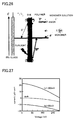
- photoelectric data thereof are such a degree as shown in Fig. 27 ( Fig. 3 of Non-Patent Document 1).
- generating efficiency is described as follows.
- Va voltage, Ia: current
- Vb, Ib current-voltage characteristic graph in which a current value is logarithmically expressed.
- NON-PATENT DOCUMENT 1 Solid state dye-sensitized TiO2 solar cell with polypyrrole as hole transport layer
- Chemistry Letters, Vol. 26, No. 5 (1997), written by Murakoshi, Kei, Kogure, Ryuichiro, Wada, Yuji and Yanagida, Shozo and published by The Chemical Society of Japan, page 472
- Fig. 3 Photocurrent-voltage characteristics of the solid cell using polypyrrole treated at -300 mV (a), and 100 mV (b).
- an aim of the present invention is to provide a hetero pn junction semiconductor having a more excellent photoelectric conversion performance, in which an electrically conductive polymer as a p-type semiconductor and nanoparticles of an inorganic oxide as an n-type semiconductor are dispersed and mixed in a closely and adequately packed state which has not been conventionally obtained, and a process for producing the same.
- Invention 1 is concerned with a hetero pn junction semiconductor constituted of an electrically conductive polymer as a p-type semiconductor and an inorganic oxide as an n-type semiconductor, which is characterized in that the electrically conductive polymer is filled among nanoparticles of the inorganic oxide so as to satisfy the following Equation 1.
- Vp / Vn X ⁇ ⁇ n / ⁇ p 0.1 ⁇ X ⁇ 10
- the hetero pn junction semiconductor of Invention 1 or 2 is one in which an electrically conductive polymer as a p-type semiconductor and nanoparticles of an inorganic oxide as an n-type semiconductor are dispersed and mixed in a closely and adequately packed state which has not been conventionally obtained, and exhibits a more excellent photoelectric conversion performance without causing mingling of a dye into the resulting product.
- a hetero pn junction semiconductor having a more excellent photoelectric conversion performance, in which an electrically conductive polymer as a p-type semiconductor and nanoparticles of an inorganic oxide as an n-type semiconductor are dispersed and mixed in a closely and adequately packed state which has not been conventionally obtained, by permeating a monomer solution that is a precursor of an electrically conductive polymer among inorganic semiconductor nanoparticles; and irradiating light upon which the nanoparticles generate holes and simultaneously applying a constant current by controlling at least one of a current density and a current application time, thereby polymerizing the monomer through a photo electrochemical reaction to form an electrically conductive polymer.
- an electrically conductive polymer as a p-type semiconductor is filled among nanoparticles of an inorganic oxide as an n-type semiconductor so as to satisfy the following ⁇ Equation 1>.
- Vp / Vn X ⁇ ⁇ n / ⁇ p 0.1 ⁇ X ⁇ 10
- the volume can be, for example, calculated by making one image of an SEM photograph of the resulting hetero pn junction semiconductor as a subject and defining an area of the inorganic oxide nanoparticles occupying therein as Vn, with an area of the electrically conductive polymer being defined as Vp. Also, as to the respective electrical conductivities, values described in handbooks or references may be adopted.
- the average particle diameter of nanoparticles of the inorganic oxide is preferably not more than 200 nm, and more preferably not more than 20 nm.
- a lower limit thereof is about 5 nm from the viewpoint of manufacture.
- an electrically conductive polymer can be formed by permeating a monomer of the electrically conductive polymer among nanoparticles of an inorganic oxide aggregated and adhered on a substrate; and thereafter, irradiating light upon which the nanoparticles generate holes and simultaneously applying a constant current by controlling at least one of a current density and a current application time, thereby polymerizing the monomer through a photo electrochemical reaction.
- the photo electrochemical reaction as referred to herein is in general one in which an oxidation-reduction reaction is carried out by utilizing holes and electrons generated due to a photo-excitation action, and in particular, in the case of using a dye, the photo electrochemical reaction is one in which an oxidation reaction is carried out by utilizing holes generated in a photo-excited state.
- the photo electrochemical reaction is corresponding to the polymerization reaction from the monomer of the electrically polymer as a p-type semiconductor into the polymer while utilizing holes generated by the inorganic oxide nanoparticles as an n-type semiconductor.
- a reaction model thereof is shown in Fig. 1 .
- TiO 2 was used as the nanoparticles of the inorganic oxide, as inorganic particles capable of working as an n-type semiconductor, tin oxide, indium oxide, zinc oxide, iron oxide, gallium oxide, tantalum oxide, tungsten oxide, cadmium oxide, silver oxide, manganese oxide, copper oxide, vanadium oxide, niobium oxide, copper indium oxide, silver indium oxide, gallium nitride or compounds thereof, and also perovskite type oxides, copper indium oxide, silver indium oxide, gallium nitride or compounds thereof may also be used.
- pyrrole was used as the monomer constituting the electrically conductive polymer
- at least one member selected from the group consisting of anilines, thiophenes, pyrroles, furans, phenylenes, phenylene vinylenes, acenes, thiophene vinylenes and isothianaphthenes may be used.
- tetraethylammonium p-toluenesulfonate (Et 4 NPTS) was exemplified below as an electrolyte, in place of this, at least member selected from the group consisting of a camphor sulfonic acid anion, a halide anion, a perchloric acid ion, a tetrafluoroboric acid ion, a hexafluoroarsenic acid ion, a sulfuric acid ion, a nitric acid ion, a thiocyanic acid ion, a hexafluorosilicic acid ion, a phosphoric acid based ion, an alkyl benzenesulfonate, an alkyl sulfonate ion, a polyacrylic acid ion, a polyvinylsulfonic acid ion, a polystyrenesulfonic acid i
- a slurry obtaining by dispersing the nanoparticles of the inorganic oxide as an n-type semiconductor in a dispersion medium is coated on a glass substrate by a coating method or the like.
- the glass substrate having the slurry coated thereon is thermally treated, thereby aggregating and adhering the nanoparticles of the inorganic oxide.
- the coated substrate is dipped in an electrolyte to allow it to react by a photo electrochemical polymerization method.
- the electrolyte the monomer of the electrically conductive polymer and a supporting salt are incorporated into a solvent.
- the irradiation light light having a wavelength and an intensity such that the nanoparticles of the inorganic oxide generate holes is used.
- ultraviolet light having a wavelength of 365 nm and an irradiation light intensity of 50 mW/cm 2 was used.
- a current density and a current application time of the current to be applied are adequately set according to values of the both, in the following Examples using titanium oxide as the nanoparticles of the inorganic oxide and pyrrole (Py) as the monomer, the current density was set from 1.27 ⁇ 10 -2 to 1.27 A/m 2 , and the current application time was set from 10 minutes to 2 hours. In the foregoing way, the desired hetero pn junction semiconductor can be obtained.
- the photo electrochemical polymerization (hereinafter referred to as "PEP") method was adopted.
- a slurry shown in Table 1 was coated in a coating amount of 0.1 (mL/cm 2 ) on the surface of an FTO (fluorine-doped tin oxide) glass substrate by a coating method.
- This slurry is one in which nanoparticles of anatase phase titanium oxide having 20 nm in an average size of primary particle and an electrical conductivity ⁇ n of 1.25 (x 10 -5 ⁇ -1 .cm -1 ) was dispersed in a content of 0.2 (g/mL) with nitric acid as a dispersion medium.
- the resultant was heated to 723 (K) at a heating rate of 15 (K/min) and then thermally treated for 30 minutes, thereby aggregating on the substrate in a particle apparent density of 0.25 (g/cm 3 ). Subsequently, this coated substrate was dipped in an electrolyte shown in Table 1, thereby executing PEP.
- electrolyte pyrrole having a concentration of 0.1 (mol/dm 3 ) was used as a monomer; tetraethylammonium p-toluenesulfonate (Et 4 NPTS) having a concentration of 0.1 (mol/dm 3 ) was used as a supporting salt; and water was used as a solvent.
- a platinum plate was used as a counter electrode, and (Ag/AgCl/saturated KCl) was used as a reference electrode.
- Potentiodynamic polarization measurement (scanning range: -1.0 to 1.5 V, scan rate: 25 mV/min) under light irradiation using a high pressure ultraviolet lamp (wavelength: 365 (nm) [strongest line], irradiation light intensity: 50 (mW/cm 2 )) and galvanostatic anodic polarization measurement under a constant current density (1.27 ⁇ 10 -2 ⁇ 1.27A/m 2 ) were carried out.
- FIG. 2 A polarization curve under light irradiation as examined by the preliminary experiment is shown in Fig. 2 . It is noted from this that the oxidation current increases at two stages in the vicinity of -0.8 V and in the vicinity of 0.5 V. It may be considered that the increase of the oxidation current from -0.8 V was caused due to the fact that electrons were supplied from the monomer into holes generated by electron excitation by light in titanium oxide. On the other hand, it may be considered that the increase of the oxidation current from 0.5 V was caused due to progress of the oxidative polymerization of polypyrrole on the substrate.
- Fig. 6b is a secondary electron image
- Fig. 6c is a reflective electron image.
- the black portion by polypyrrole is localized. Scanning electroscopic photographs of the section of the same specimen are shown in Fig. 7 . It is noted that voids which appear gray are present among white titanium oxides, and black polypyrrole is formed in a part thereof.
- the prepared film of Experiment No. 1 had ⁇ p of 1.98 ( ⁇ 10 -5 ⁇ -1 .cm -1 ), a particle apparent density of 0.125 (g/cm 3 ), X of 0.74 and a contact area of 6.3 %. This example satisfies the range of X in the foregoing equation, and a hetero pn junction film having an excellent photoelectric conversion performance was obtained without using a dye.
- Figs. 11a to 11c Scanning electron microscopic images of the surface of the same specimen are shown in Figs. 11a to 11c . It is noted that the black portion by polypyrrole increases as compared with that in Fig. 6c . Scanning electroscopic photographs of the section of the same specimen are shown in Fig. 12 . It is noted that voids which appear gray are present among white titanium oxides, and black polypyrrole is formed in a part thereof. It is noted that the black area increases as compared with that in Fig. 7 .
- the prepared film of Experiment No.2 had ⁇ p of 1.98 (x 10 -5 ⁇ -1 .cm -1 ), a particle apparent density of 0.125 (g/cm 3 ), X of 1.11 and a contact area of 9.5 %.
- Figs. 16a to 16c Scanning electron microscopic photographs of the surface of the same specimen are shown in Figs. 16a to 16c . It is noted that the black portion by polypyrrole increases as compared with that in Fig. 11c . Scanning electroscopic photographs of the section of the same specimen are shown in Fig. 17 . It is noted that voids which appear gray are present among white titanium oxides, and black polypyrrole is formed in a part thereof. It is noted that the black area increases as compared with that in Fig. 12 .
- the prepared film of Experiment No.3 had ⁇ p of 1.98 ( ⁇ 10 -5 ⁇ -1 .cm -1 ), a particle apparent density of 0.125 (g/cm 3 ), X of 1.48 and a contact area of 12.6 %.
- the prepared film of Experiment No.4 had ⁇ p of 1.98 ( ⁇ 10 -5 ⁇ -1 .cm -1 ), a particle apparent density of 0.125 (g/cm 3 ), X of 1.18 and a contact area of 10 %.
- the current density is 1.27 A/m 2
- the potential after a gradual increase of the polarization potential to around -0.2 V, the potential rapidly increased to around 0.5 V and became almost constant ( Fig. 20 ).
- deposition of polypyrrole was observed in the vicinity of the substrate. When combined with the results of the polarization curve, it may be considered that the formation of pyrrole proceeded on titanium oxide around -0.2 V and on the substrate at 0.5 V, respectively.
- the electrochemical measurement was carried out using a three-electrode cell having an open window for installing a working electrode.
- the working electrode was prepared in the following manner. A suspension containing titanium oxide (anatase, 20 nm) was coated on a transparent electrically conductive oxide (TCO) glass substrate. After thermally treating at 723 K for 30 minutes, the resultant was dipped in an ethanol solution containing an Ru dye (N719) at room temperature for 24 hours. Pyrrole as a precursor of the polymer and polyethylene glycol (PEG, molecular weight: 200) containing, as a supporting salt, tetraethylammonium p-toluenesulfonate serving as a dopant were used for the electrolyte.
- PEG polyethylene glycol
- a platinum plate was used as a counter electrode, and an Ag/AgCl/saturated KCl solution was used as a reference electrode.
- a potential of the working electrode is shown relative to a potential of a standard hydrogen electrode (SHE). Visible light was introduced from the back side of the working electrode by using a solar simulator. Linear sweep voltammetry was carried out at a scan rate of 25 mV/min at from a immersion potential to 2.0 V. Chronopotentiometry was carried out at a current density of from 0.75 to 75 ⁇ A/cm 2 . SEM was used for the surface observation of the specimen. Fig.
- Fig. 21 is an SEM image of a specimen after carrying out the chronopotentiometry at a current density of 0.75 ⁇ A/cm 2 for 60 minutes;
- Fig. 22 is an SEM image of a specimen after carrying out the chronopotentiometry at a current density of 7.5 ⁇ A/cm 2 for 60 minutes;
- Fig. 23 is an SEM image of a specimen after carrying out the chronopotentiometry at a current density of 75 ⁇ A/cm 2 for 10 minutes. It is noted that the larger the quantity of electricity is, the more polypyrrole (block portion on the top) increased, and the polymerization proceeds.
- FIG. 24 Anodic polarization curves obtained under some conditions are shown in Fig. 24 .
- the immersion potential under light irradiation was less noble than that under dark.
- the current (photocurrent) under light irradiation rapidly increased by slight anodic polarization from the immersion potential. It may be considered that this is caused due to the fact that holes generated by photo-excitation cause an anodic reaction.
- the photocurrent observed up to -0.25 V is larger than that when pyrrole is not contained.
- the dependency of the photocurrent upon the polarization potential is identical within the range of from -0.25 V to 1.6 V regardless of the presence or absence of pyrrole.
- PEG contributes to the photoanodic reaction from -0.25 V to 1.6 V.
- the photocurrent exhibited a substantially constant value, whereas when pyrrole was contained, the photocurrent increased. It may be considered that this increase of the photocurrent is caused due to electrolytic oxidative polymerization of pyrrole on the TCO substrate. In actuality, an abrupt increase of the anodic current at 1.3 V or higher was observed under dark.
- the chronopotentiometry is hereunder described.
- the chronopotentiometry as referred to herein is a technique in which a potential change is observed at the time of allowing a constant current to flow, thereby electrochemically analyzing a reaction process.
- the electrode potential increases with time at the beginning of polymerization. In this time, polymerization of pyrrole by a dye sensitized photoanodic reaction proceeds. After the potential increase at the beginning of polarization, with respect to the two plateaus in potential, in the plateau on a low potential, the anodic reaction of electrolyte by holes generated by photo-excitation proceeds, whereas in the plateau on a high potential, electrolytic oxidative polymerization proceeds on the TCO substrate.
- the reaction rate as referred to herein is a polymerization rate of an electrically conductive polymer, and it may be expected that polymers having various polymerization degrees are formed.
- the polymerization is carried out on the basis of a steady polarization (potential-current) curve while keeping the current (reaction rate) constant, it may be considered that a structure containing a more uniform electrically conductive polymer is obtained.
- a monomer releases an electron and is polymerized into a polymer according to the following scheme.
- a dopant is taken into the polymer.
Landscapes
- Engineering & Computer Science (AREA)
- Chemical & Material Sciences (AREA)
- Inorganic Chemistry (AREA)
- Physics & Mathematics (AREA)
- Electromagnetism (AREA)
- Crystallography & Structural Chemistry (AREA)
- Nanotechnology (AREA)
- Manufacturing & Machinery (AREA)
- Hybrid Cells (AREA)
- Photovoltaic Devices (AREA)
Abstract
Description
- The present invention relates to a hetero pn junction semiconductor, especially a hetero pn junction semiconductor constituted of an electrically conductive polymer as a p-type semiconductor and an inorganic oxide as an n-type semiconductor, which can be utilized for diodes, solar cells and the like.
- A material in which an electrically conductive polymer as a p-type semiconductor and an inorganic compound as an n-type semiconductor are complexed on a nano level is expected to act as a solar cell having a hetero pn junction. For that reason, it has been attempted to create the subject solar cell by the methods described in
Patent Documents 1 to 3; however, an optimal fine structure or interface structure therefor has not been elucidated yet. Incidentally, according to Non-PatentDocument 1, photoelectric data thereof are such a degree as shown inFig. 27 (Fig. 3 of Non-Patent Document 1). Furthermore, in order to increase a contact area, it may be considered that it is effective to use an agglomerated structure of nanoparticles as one of junction structures; however, since it is difficult to densely fill solid phases each other, a sufficient effect is not obtained, and such a way is only at an ideal stage yet. - In
Patent Document 4, generating efficiency is described as follows.
The generating efficiency is calculated according to the following equation:
(n represents a diode factor; e represents an elementary electric charge; k represents a Boltzmann constant; T represents an absolute temperature; arbitrary two points (Va: voltage, Ia: current) and (Vb, Ib) of a current-voltage characteristic graph in which a current value is logarithmically expressed.)
Then, when n is equal to 1 theequation 2 is an ideal diode equation, and as an electric behavior of junction is deviated from the ideal sate, the value of n becomes large."
Furthermore, it is also described that: - "This diode factor n mainly represents a junction density of the pn junction interface, and when the junction density is high, then n is equal to 1, thereby revealing an ideal interface state. When the junction density is low, the rectification properties become deteriorated. In organic semiconductors, n was conventionally a value of from 2 to 3."
-
-
PATENT DOCUMENT 1 -
JP-A-2006-016582 -
PATENT DOCUMENT 2 -
JP-A-2003-142168 -
PATENT DOCUMENT 3 -
JP-A-2004-182819 -
PATENT DOCUMENT 4 -
JP-A-2004-071682 - NON-PATENT
DOCUMENT 1 "Solid state dye-sensitized TiO2 solar cell with polypyrrole as hole transport layer", Chemistry Letters, Vol. 26, No. 5 (1997), written by Murakoshi, Kei, Kogure, Ryuichiro, Wada, Yuji and Yanagida, Shozo and published by The Chemical Society of Japan, page 472,Fig. 3 : Photocurrent-voltage characteristics of the solid cell using polypyrrole treated at -300 mV (a), and 100 mV (b). - In view of such circumstances, an aim of the present invention is to provide a hetero pn junction semiconductor having a more excellent photoelectric conversion performance, in which an electrically conductive polymer as a p-type semiconductor and nanoparticles of an inorganic oxide as an n-type semiconductor are dispersed and mixed in a closely and adequately packed state which has not been conventionally obtained, and a process for producing the same.
-
Invention 1 is concerned with a hetero pn junction semiconductor constituted of an electrically conductive polymer as a p-type semiconductor and an inorganic oxide as an n-type semiconductor, which is characterized in that the electrically conductive polymer is filled among nanoparticles of the inorganic oxide so as to satisfy the followingEquation 1.
- Vp = Volume of the electrically conductive polymer as a p-type semiconductor
- σp = Electrical conductivity of the electrically conductive polymer as a p-type semiconductor
- Vn = Volume of the inorganic oxide nanoparticles as an n-type semiconductor
- σn = Electrical conductivity of the inorganic oxide nanoparticles as an n-type semiconductor
- The hetero pn junction semiconductor of
Invention
Also, according to the process ofInvention 3, in the present invention, it is possible to produce a hetero pn junction semiconductor having a more excellent photoelectric conversion performance, in which an electrically conductive polymer as a p-type semiconductor and nanoparticles of an inorganic oxide as an n-type semiconductor are dispersed and mixed in a closely and adequately packed state which has not been conventionally obtained, by permeating a monomer solution that is a precursor of an electrically conductive polymer among inorganic semiconductor nanoparticles; and irradiating light upon which the nanoparticles generate holes and simultaneously applying a constant current by controlling at least one of a current density and a current application time, thereby polymerizing the monomer through a photo electrochemical reaction to form an electrically conductive polymer. -
-
Fig. 1 is a schematic model showing photoelectrolytic oxidative polymerization. -
Fig. 2 is a polarization curve under light irradiation. -
Fig. 3 shows a change in potential with time while performing non-light irradiation → light irradiation → light irradiation + current application in Experiment No. 1 (at 1.27 × 10⁻² A/m2 for 1.0 hour). -
Fig. 4 is an appearance of specimen after the experiment in Experiment No. 1 (at 1.27 × 10⁻²A/m2 for 1.0 hour). -
Fig. 5 is a photograph of specimen surface by an optical microscope in Experiment No. 1 (at 1.27 × 10⁻² A/m2 for 1.0 hour). -
Fig. 6 is an image of specimen surface by scanning electron microscope in Experiment No. 1 (at 1.27 × 10⁻² A/m2 for 1.0 hour). -
Fig. 7 is a cross-sectional image of specimen by scanning electron microscope in Experiment No. 1 (at 1.27 × 10⁻² A/m2 for 1.0 hour). -
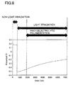
Fig. 8 shows a change in potential with time while performing non-light irradiation → light irradiation → light irradiation + current application in Experiment No. 2 (at 1.27 × 10⁻² A/m2 for 1.5 hours). -
Fig. 9 is an appearance of specimen after the experiment in Experiment No. 2 (at 1.27 × 10⁻² A/m2 for 1.5 hours). -
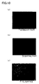
Fig. 10 is a photograph of specimen surface by an optical microscope in Experiment No. 2 (at 1.27 × 10⁻² A/m2 for 1.5 hours). -
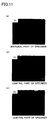
Fig. 11 is an image of specimen surface by scanning electron microscope in Experiment No. 2 (at 1.27 × 10⁻² A/m2 for 1.5 hours). -
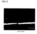
Fig. 12 is a cross-sectional image by scanning electron microscope in Experiment No. 2 (at 1.27 × 10⁻² A/m2 for 1.5 hours). -
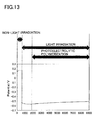
Fig. 13 shows a change in potential with time while performing non-light irradiation → light irradiation → light irradiation + current application in Experiment No. 3 (at 1.27 × 10⁻² A/m2 for 2.0 hours). -
Fig. 14 is an appearance of specimen after the experiment in Experiment No.3 (at 1.27 × 10⁻² A/m2 for 2.0 hours). -
Fig. 15 shows a change in potential with a constant current to flow in Experiment No. 3 (at 1.27 × 10⁻² A/m2 for 2.0 hours). -
Fig. 16 is an image of specimen surface by scanning electron microscope in Experiment No. 3 (at 1.27 × 10⁻² A/m2 for 2.0 hours). -
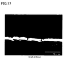
Fig. 17 is a cross-sectional image by scanning electron microscope in Experiment No. 3 (at 1.27 × 10⁻² A/m2 for 2.0 hours). -
Fig. 18 shows a change in potential with time while performing non-light irradiation → light irradiation → light irradiation + current application in Experiment No. 8 (at 1.27 A/m2 for 10 minutes). -
Fig. 19 is an image of specimen surface by scanning electron microscope in Experiment No. 8 (at 1.27 A/m2 for 10 minutes). -
Fig. 20 shows a change in potential with time while performing non-light irradiation → light irradiation → light irradiation + current application in Experiment No. 9 (at 1.27 A/m2 for 30 minutes). -
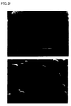
Fig. 21 is an SEM image of a specimen surface after applying current at 7.5 µA/cm2 for 60 minutes in Example 2 (top: back scattering image, bottom: secondary electron image). -
Fig. 22 is an SEM image of a specimen surface after applying current at 75 µA/cm2 for 10 minutes in Example 2 (top: back scattering image, bottom: secondary electron image). -
Fig. 23 is an SEM image of a specimen surface after applying current at 0.75 µA/cm2 for 60 minutes in Example 2 (top: back scattering image, bottom: secondary electron image). -
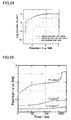
Fig. 24 is anodic polarization curves in Example 2. -
Fig. 25 is chronopotentiometric curves in Example 2. -
Fig. 26 is a schematic view explaining a polymerization process of a polymer by a photoanodic reaction. -
Fig. 27 isFig. 3 ofNon-Patent Document 1. - In the hetero pn junction semiconductor of the present invention, an electrically conductive polymer as a p-type semiconductor is filled among nanoparticles of an inorganic oxide as an n-type semiconductor so as to satisfy the following <
Equation 1>.
- Vp = Volume of the electrically conductive polymer as a p-type semiconductor
- σp = Electrical conductivity of the electrically conductive polymer as a p-type semiconductor
- Vn = Volume of the inorganic oxide nanoparticles as an n-type semiconductor
- σn = Electrical conductivity of the inorganic oxide nanoparticles as an n-type semiconductor
- When X is too small, though the amount of the required electrically conductive polymer as a p-type semiconductor may be decreased, in actual, it is difficult to ensure an electrical conductive path by connecting electrically conductive polymers. When X is surplus, even if all of voids among the inorganic oxide nanoparticles as an n-type semiconductor are filled with the electrically conductive polymer as a p-type semiconductor, a balance of electrical resistance among the semiconductors conspicuously breaks down. In consequence, it is desirable that X falls within the foregoing range.
- In this
Equation 1, the volume can be, for example, calculated by making one image of an SEM photograph of the resulting hetero pn junction semiconductor as a subject and defining an area of the inorganic oxide nanoparticles occupying therein as Vn, with an area of the electrically conductive polymer being defined as Vp. Also, as to the respective electrical conductivities, values described in handbooks or references may be adopted. - In view of the fact that the smaller the average particle diameter of the nanoparticles of the inorganic oxide is, the more favorable results are obtainable, it is desirable that the average particle diameter of nanoparticles of the inorganic oxide is preferably not more than 200 nm, and more preferably not more than 20 nm. A lower limit thereof is about 5 nm from the viewpoint of manufacture.
Light having a wavelength of the size of the particle diameter of the nanoparticles or more, for example, ultraviolet to visible lights, can transmit therethrough without being scattered by the particles. Among the transmitted lights, light having a wavelength of band gap energy or more contributes to a photo-excitation reaction at the absorption.
Therefore, it is effective to take a large wavelength width of light capable of being transmitted by making the diameter of the nanoparticles small as far as possible. - As to the hetero pn junction semiconductor, an electrically conductive polymer can be formed by permeating a monomer of the electrically conductive polymer among nanoparticles of an inorganic oxide aggregated and adhered on a substrate; and thereafter, irradiating light upon which the nanoparticles generate holes and simultaneously applying a constant current by controlling at least one of a current density and a current application time, thereby polymerizing the monomer through a photo electrochemical reaction.
- The photo electrochemical reaction as referred to herein is in general one in which an oxidation-reduction reaction is carried out by utilizing holes and electrons generated due to a photo-excitation action, and in particular, in the case of using a dye, the photo electrochemical reaction is one in which an oxidation reaction is carried out by utilizing holes generated in a photo-excited state. Here, the photo electrochemical reaction is corresponding to the polymerization reaction from the monomer of the electrically polymer as a p-type semiconductor into the polymer while utilizing holes generated by the inorganic oxide nanoparticles as an n-type semiconductor. A reaction model thereof is shown in
Fig. 1 . - Though in the following Examples, TiO2 was used as the nanoparticles of the inorganic oxide, as inorganic particles capable of working as an n-type semiconductor, tin oxide, indium oxide, zinc oxide, iron oxide, gallium oxide, tantalum oxide, tungsten oxide, cadmium oxide, silver oxide, manganese oxide, copper oxide, vanadium oxide, niobium oxide, copper indium oxide, silver indium oxide, gallium nitride or compounds thereof, and also perovskite type oxides, copper indium oxide, silver indium oxide, gallium nitride or compounds thereof may also be used.
- Also, though in the following Example, pyrrole was used as the monomer constituting the electrically conductive polymer, in addition to the above, at least one member selected from the group consisting of anilines, thiophenes, pyrroles, furans, phenylenes, phenylene vinylenes, acenes, thiophene vinylenes and isothianaphthenes may be used.
- Also, though tetraethylammonium p-toluenesulfonate (Et4NPTS) was exemplified below as an electrolyte, in place of this, at least member selected from the group consisting of a camphor sulfonic acid anion, a halide anion, a perchloric acid ion, a tetrafluoroboric acid ion, a hexafluoroarsenic acid ion, a sulfuric acid ion, a nitric acid ion, a thiocyanic acid ion, a hexafluorosilicic acid ion, a phosphoric acid based ion, an alkyl benzenesulfonate, an alkyl sulfonate ion, a polyacrylic acid ion, a polyvinylsulfonic acid ion, a polystyrenesulfonic acid ion and a poly(2-acrylamide-2-methylpropanesulfonic acid) ion may be used.
- In the case of producing the hetero pn junction semiconductor of the present invention, first of all, for example, a slurry obtaining by dispersing the nanoparticles of the inorganic oxide as an n-type semiconductor in a dispersion medium is coated on a glass substrate by a coating method or the like.
Subsequently, the glass substrate having the slurry coated thereon is thermally treated, thereby aggregating and adhering the nanoparticles of the inorganic oxide.
Thereafter, the coated substrate is dipped in an electrolyte to allow it to react by a photo electrochemical polymerization method. As to the electrolyte, the monomer of the electrically conductive polymer and a supporting salt are incorporated into a solvent. As the irradiation light, light having a wavelength and an intensity such that the nanoparticles of the inorganic oxide generate holes is used. In the following Examples, ultraviolet light having a wavelength of 365 nm and an irradiation light intensity of 50 mW/cm2 was used. Though a current density and a current application time of the current to be applied are adequately set according to values of the both, in the following Examples using titanium oxide as the nanoparticles of the inorganic oxide and pyrrole (Py) as the monomer, the current density was set from 1.27 × 10⁻² to 1.27 A/m2, and the current application time was set from 10 minutes to 2 hours.
In the foregoing way, the desired hetero pn junction semiconductor can be obtained. - For the preparation of a hetero pn junction film, the photo electrochemical polymerization (hereinafter referred to as "PEP") method was adopted.
First of all, a slurry shown in Table 1 was coated in a coating amount of 0.1 (mL/cm2) on the surface of an FTO (fluorine-doped tin oxide) glass substrate by a coating method. This slurry is one in which nanoparticles of anatase phase titanium oxide having 20 nm in an average size of primary particle and an electrical conductivity σn of 1.25 (x 10-5 Ω-1.cm-1) was dispersed in a content of 0.2 (g/mL) with nitric acid as a dispersion medium.
After coating, the resultant was heated to 723 (K) at a heating rate of 15 (K/min) and then thermally treated for 30 minutes, thereby aggregating on the substrate in a particle apparent density of 0.25 (g/cm3).
Subsequently, this coated substrate was dipped in an electrolyte shown in Table 1, thereby executing PEP. As to the electrolyte, pyrrole having a concentration of 0.1 (mol/dm3) was used as a monomer; tetraethylammonium p-toluenesulfonate (Et4NPTS) having a concentration of 0.1 (mol/dm3) was used as a supporting salt; and water was used as a solvent. At that time, a platinum plate was used as a counter electrode, and (Ag/AgCl/saturated KCl) was used as a reference electrode.
Potentiodynamic polarization measurement (scanning range: -1.0 to 1.5 V, scan rate: 25 mV/min) under light irradiation using a high pressure ultraviolet lamp (wavelength: 365 (nm) [strongest line], irradiation light intensity: 50 (mW/cm2)) and galvanostatic anodic polarization measurement under a constant current density (1.27×10⁻²∼1.27A/m2) were carried out.
Also, as to the prepared specimen, observation of a surface and a section by an optical microscope (OM) and a scanning electron microscope (SEM) was carried out.
Characteristics thereof were measured in the following ways.
The particle diameter was measured by using X-ray diffraction measurement, laser diffraction particle diameter distribution measurement and a Coulter counter.
The particle (apparent) density was determined by using sectional image analysis, a mercury porosimeter, a pycnometer and weight and thickness measurements. Incidentally, Experiments Nos. 6 and 8 to 10 of Table 1 are comparative examples for the purpose of clarifying the present invention. -
[Table 1] Experiment No. 1 2 3 4 5 6 7 8 9 10 Nanoparticle Primary particle diameter (nm) diameter 20 " " " " " " " " " Material TiO2* " " " " " " " " " *σn 1,25 " " " " " " " " " Slurry Dispersion medium Nitric acid " " " " " " " " " NP* (g/mL) 0.2 " " " " " " " " " Coating amount(mL/cm2) 0.1 " " " " " " " " " Thermal treatment Treatment temperature (K) 723 " " " " " " " " " Heating rate(K/min) 15 " " " " " " " " " Treatment time(hr) 1/2 " " " " " " " " " Particle apparent density (g/cm3) 0.25 " " " " " " " " " Electrolyte (1) Material PY " " " " " " " " " Concentration* 0.1 " " " " " " " " " (2) Material Et4NPTS " " " " " " " " " Concentration* 0.1 " " " " " " " " " Solvent Water " " " " " " " " " PEP Irradiation light wavelength (nm: strongest line) 365 " " " " " " " " " Irradiation light intensity (mW/cm2) 50 " " " " " " " " " Current density (× 10-1 A/m2) 0.127 0.127 0.127 1.27 1.27 1.27 6.35 12.7 12.7 12.7 Treatment time (hr) 1 1+1/2 2 1/6 1 1+1/2 1/6 1/6 1/2 1 Prepared film (3) Material PP " " " " " " " " " *σp 1.98 " " " " " " " " " Particle apparent density (g/cm3) 0.125 " " " " " " " " " Contact area (%) 6.3 9.5 12.6 10 63 95 50 100 100 100 *X 0.74 1.11 1.48 1.18 7.4 11.1 5.9 11.8 37 74 NP*: Nanoparticle content TiO2*: TiO2 anatase phase Each of *σn, *σp and *X is algebra in the Equation 1, and each of the units of *σn and *σp is (x 10-5 Ω-1-cm-1). Et4NPTS: Tetraethylammonium p-toluenesulfonate UVL: Light by high pressure ultraviolet lamp (1) Monomer PY: Pyrrole (2) Supporting salt PP: Polypyrrole (3) Electrically conductive polymer Concentration*: The unit is (md/dm3) - A polarization curve under light irradiation as examined by the preliminary experiment is shown in
Fig. 2 . It is noted from this that the oxidation current increases at two stages in the vicinity of -0.8 V and in the vicinity of 0.5 V. It may be considered that the increase of the oxidation current from -0.8 V was caused due to the fact that electrons were supplied from the monomer into holes generated by electron excitation by light in titanium oxide. On the other hand, it may be considered that the increase of the oxidation current from 0.5 V was caused due to progress of the oxidative polymerization of polypyrrole on the substrate. - Changes with time of an immersion potential under non-light irradiation and light irradiation and a potential under galvanostatic polarization (at a current density of 1.27 × 10⁻² A/m2 for one hour (Experiment No.1)) are shown in
Fig. 3 . An appearance of the specimen after the polarization is shown inFig. 4 . It is noted that the specimen surface is slightly blackened. Also, photographs of the surface of the same specimen by an optical microscope are shown inFigs. 5a to 5c . It is noted that in the foregoing blackened portion, a white portion by titanium oxide and a black portion by polypyrrole coexist. Scanning electron microscopic photographs of the surface of the same specimen are shown inFigs. 6a to 6c. Fig. 6b is a secondary electron image, andFig. 6c is a reflective electron image. It is noted that the black portion by polypyrrole is localized. Scanning electroscopic photographs of the section of the same specimen are shown inFig. 7 . It is noted that voids which appear gray are present among white titanium oxides, and black polypyrrole is formed in a part thereof.
The prepared film of Experiment No. 1 had σp of 1.98 (× 10-5 Ω-1.cm-1), a particle apparent density of 0.125 (g/cm3), X of 0.74 and a contact area of 6.3 %. This example satisfies the range of X in the foregoing equation, and a hetero pn junction film having an excellent photoelectric conversion performance was obtained without using a dye. - Changes with time of an immersion potential under non-light irradiation and light irradiation and a potential under galvanostatic polarization (at a current density of 1.27 × 10⁻² A/m2 for 1.5 hours (Experiment No. 2)) are shown in
Fig. 8 . An appearance of the specimen after the polarization is shown inFig. 9 . It is noted that a blackened portion of the specimen surface increases as compared with that inFig. 4 . Also, photographs of the surface of the same specimen by an optical microscope are shown inFigs. 10a to 10c . It is noted that in the foregoing blackened portion, a white portion by titanium oxide and a black portion by polypyrrole coexist. Scanning electron microscopic images of the surface of the same specimen are shown inFigs. 11a to 11c . It is noted that the black portion by polypyrrole increases as compared with that inFig. 6c . Scanning electroscopic photographs of the section of the same specimen are shown inFig. 12 . It is noted that voids which appear gray are present among white titanium oxides, and black polypyrrole is formed in a part thereof. It is noted that the black area increases as compared with that inFig. 7 .
The prepared film of Experiment No.2 had σp of 1.98 (x 10-5 Ω-1.cm-1), a particle apparent density of 0.125 (g/cm3), X of 1.11 and a contact area of 9.5 %. - Changes with time of an immersion potential under non-light irradiation and light irradiation and a potential under galvanostatic polarization (at a current density of 1.27 × 10⁻² A/m2 for 2.0 hours (Experiment No. 3)) are shown in
Fig. 13 . An appearance of the specimen after the polarization is shown inFig. 14 . It is noted that a blackened portion of the specimen surface increases as compared with that inFig. 9 . Also, photographs of the surface of the same specimen by an optical microscope are shown inFigs. 15a to 15c . It is noted that in the foregoing blackened portion, a white portion by titanium oxide and a black portion by polypyrrole coexist. Scanning electron microscopic photographs of the surface of the same specimen are shown inFigs. 16a to 16c . It is noted that the black portion by polypyrrole increases as compared with that inFig. 11c . Scanning electroscopic photographs of the section of the same specimen are shown inFig. 17 . It is noted that voids which appear gray are present among white titanium oxides, and black polypyrrole is formed in a part thereof. It is noted that the black area increases as compared with that inFig. 12 .
The prepared film of Experiment No.3 had σp of 1.98 (× 10-5 Ω-1.cm-1), a particle apparent density of 0.125 (g/cm3), X of 1.48 and a contact area of 12.6 %. - Changes with time of an immersion potential under non-light irradiation and light irradiation and a potential under galvanostatic polarization (at a current density of 1.27 A/m2 for 10 minutes (Experiment No. 4)) are shown in
Fig. 18 . Scanning electron microscopic photographs of the surface of the specimen surface after the polarization are shown inFigs. 19a to 19b . It is noted that the black portion by polypyrrole increases as compared with that inFig. 16c , and almost all portions are covered black (for example,Fig. 19b ).
The prepared film of Experiment No.4 had σp of 1.98 (× 10-5 Ω-1.cm-1), a particle apparent density of 0.125 (g/cm3), X of 1.18 and a contact area of 10 %.
Incidentally, in the case where the current density is 1.27 A/m2, after a gradual increase of the polarization potential to around -0.2 V, the potential rapidly increased to around 0.5 V and became almost constant (Fig. 20 ). Also, in the specimen after the polarization, deposition of polypyrrole was observed in the vicinity of the substrate. When combined with the results of the polarization curve, it may be considered that the formation of pyrrole proceeded on titanium oxide around -0.2 V and on the substrate at 0.5 V, respectively. - The preparation of polypyrrole by a photo electrochemical polymerization method using a substrate having a titanium oxide film prepared on an FTO glass was investigated. As a result, it became clear that the deposition of polypyrrole on titanium oxide depends upon its potential. Also, it was noted that the growth process depends upon the current density and the current impression time.
- As to the prepared films of Experiments Nos. 5 to 10, observation and measurement were carried out in the same ways as those described above. Values of X and the contact area were those shown in Table 1.
- The electrochemical measurement was carried out using a three-electrode cell having an open window for installing a working electrode. The working electrode was prepared in the following manner. A suspension containing titanium oxide (anatase, 20 nm) was coated on a transparent electrically conductive oxide (TCO) glass substrate. After thermally treating at 723 K for 30 minutes, the resultant was dipped in an ethanol solution containing an Ru dye (N719) at room temperature for 24 hours. Pyrrole as a precursor of the polymer and polyethylene glycol (PEG, molecular weight: 200) containing, as a supporting salt, tetraethylammonium p-toluenesulfonate serving as a dopant were used for the electrolyte.
A platinum plate was used as a counter electrode, and an Ag/AgCl/saturated KCl solution was used as a reference electrode. In this Example, a potential of the working electrode is shown relative to a potential of a standard hydrogen electrode (SHE). Visible light was introduced from the back side of the working electrode by using a solar simulator.
Linear sweep voltammetry was carried out at a scan rate of 25 mV/min at from a immersion potential to 2.0 V. Chronopotentiometry was carried out at a current density of from 0.75 to 75 µA/cm2.
SEM was used for the surface observation of the specimen.Fig. 21 is an SEM image of a specimen after carrying out the chronopotentiometry at a current density of 0.75 µA/cm2 for 60 minutes;Fig. 22 is an SEM image of a specimen after carrying out the chronopotentiometry at a current density of 7.5 µA/cm2 for 60 minutes; andFig. 23 is an SEM image of a specimen after carrying out the chronopotentiometry at a current density of 75 µA/cm2 for 10 minutes.
It is noted that the larger the quantity of electricity is, the more polypyrrole (block portion on the top) increased, and the polymerization proceeds. - Anodic polarization curves obtained under some conditions are shown in
Fig. 24 . The immersion potential under light irradiation was less noble than that under dark. The current (photocurrent) under light irradiation rapidly increased by slight anodic polarization from the immersion potential. It may be considered that this is caused due to the fact that holes generated by photo-excitation cause an anodic reaction.
It is noted that when the pyrrole is contained in the electrolyte, the photocurrent observed up to -0.25 V is larger than that when pyrrole is not contained. Also, it is noted that the dependency of the photocurrent upon the polarization potential is identical within the range of from -0.25 V to 1.6 V regardless of the presence or absence of pyrrole. In consequence, it may be conjectured that PEG contributes to the photoanodic reaction from -0.25 V to 1.6 V. At 1.6 V or higher, when pyrrole was not present in the electrolyte, the photocurrent exhibited a substantially constant value, whereas when pyrrole was contained, the photocurrent increased. It may be considered that this increase of the photocurrent is caused due to electrolytic oxidative polymerization of pyrrole on the TCO substrate. In actuality, an abrupt increase of the anodic current at 1.3 V or higher was observed under dark. - From the results of the chronopotentiometry under the light irradiation (
Fig. 25 ), the electrode potential increased with time at the beginning of polarization, and its duration time depended upon the current density. The presence of an organic material was confirmed on the surface of the working electrode after the polarization at 7.5 µA/cm2 for one hour (Fig. 25 ). From these results, it may be considered that in this duration time, the polymerization of Py due to a dye sensitized photoanodic reaction proceeds. Also, after the potential increase at the beginning of polarization, two plateaus in potential were observed. It may be conjectured that in the plateau on the low potential, the anodic reaction of electrolyte by holes generated by photo-excitation proceeds, whereas in the plateau on the high potential, electrolytic oxidative polymerization proceeds on the TCO substrate. - The chronopotentiometry is hereunder described.
The chronopotentiometry as referred to herein is a technique in which a potential change is observed at the time of allowing a constant current to flow, thereby electrochemically analyzing a reaction process.
The electrode potential increases with time at the beginning of polymerization. In this time, polymerization of pyrrole by a dye sensitized photoanodic reaction proceeds.
After the potential increase at the beginning of polarization, with respect to the two plateaus in potential, in the plateau on a low potential, the anodic reaction of electrolyte by holes generated by photo-excitation proceeds, whereas in the plateau on a high potential, electrolytic oxidative polymerization proceeds on the TCO substrate. - So far, a structure of inorganic semiconductor (titanium oxide)/dye/electrically conductive polymer (polypyrrole) was reported. However, in that report, only the potential is controlled at the time of causing a photo electrochemical reaction. In view of the fact that the potential varies depending upon a site (resistance) within the structure, a current value (namely, a reaction rate) locally changes. That is, the reaction rate as referred to herein is a polymerization rate of an electrically conductive polymer, and it may be expected that polymers having various polymerization degrees are formed.
In the present invention, since the polymerization is carried out on the basis of a steady polarization (potential-current) curve while keeping the current (reaction rate) constant, it may be considered that a structure containing a more uniform electrically conductive polymer is obtained. - Incidentally, the polymerization process of a polymer due to the photoanodic reaction is hereunder described by reference to
Fig. 26 .
A monomer releases an electron and is polymerized into a polymer according to the following scheme.
In order to make a balance of electric charges, a dopant is taken into the polymer. - Monomer → Polymer + Electron
- (Oxidation reaction = Polymerization reaction)
-
- (P) Electrically conductive polymer (black portion)
- (N) Nanoparticle (white portion)
- (H) Hole into which the electrically conductive polymer could not be filled (black portion whose depth is seen)
The photocurrent is one of factors determining the generating efficiency together with the voltage. In consequence, the adhesive area is an important factor influencing the generating efficiency.
Claims (3)
- A hetero pn junction semiconductor constituted of an electrically conductive polymer as a p-type semiconductor and an inorganic oxide as an n-type semiconductor, which is characterized in that the electrically conductive polymer is filled among nanoparticles of the inorganic oxide so as to satisfy the following Equation 1:
 Vp = Volume of the electrically conductive polymer as a p-type semiconductorσp = Electrical conductivity of the electrically conductive polymer as a p-type semiconductorVn = Volume of the inorganic oxide nanoparticles as an n-type semiconductorσn = Electrical conductivity of the inorganic oxide nanoparticles as an n-type semiconductor
 - The hetero pn junction semiconductor according to claim 1, which is characterized in that an average particle size of the nanoparticles of the inorganic oxide is not more than 200 nm.
- A process for producing the hetero pn junction semiconductor according to claim 1 or 2, which is characterized by permeating a monomer of an electrically conductive polymer among nanoparticles of an inorganic oxide aggregated and adhered on a substrate; and thereafter, irradiating light upon which the nanoparticles generate holes and simultaneously applying a constant current by controlling at least one of a current density and a current application time, thereby polymerizing the monomer through a photo electrochemical reaction to form an electrically conductive polymer and thereby producing a hetero pn junction semiconductor.
Applications Claiming Priority (3)
| Application Number | Priority Date | Filing Date | Title |
|---|---|---|---|
| JP2009045406 | 2009-02-27 | ||
| JP2009132693 | 2009-06-02 | ||
| PCT/JP2010/053152 WO2010098464A1 (en) | 2009-02-27 | 2010-02-26 | HETERO Pn JUNCTION SEMICONDUCTOR AND PROCESS FOR PRODUCING SAME |
Publications (2)
| Publication Number | Publication Date |
|---|---|
| EP2403006A1 true EP2403006A1 (en) | 2012-01-04 |
| EP2403006A4 EP2403006A4 (en) | 2014-04-02 |
Family
ID=42665668
Family Applications (1)
| Application Number | Title | Priority Date | Filing Date |
|---|---|---|---|
| EP10746343.2A Withdrawn EP2403006A4 (en) | 2009-02-27 | 2010-02-26 | HETERONJUNCTION SEM SEMICONDUCTOR AND METHOD FOR PRODUCING THE SAME |
Country Status (4)
| Country | Link |
|---|---|
| US (1) | US8563975B2 (en) |
| EP (1) | EP2403006A4 (en) |
| JP (1) | JPWO2010098464A1 (en) |
| WO (1) | WO2010098464A1 (en) |
Families Citing this family (6)
| Publication number | Priority date | Publication date | Assignee | Title |
|---|---|---|---|---|
| KR20150003181A (en) * | 2012-03-14 | 2015-01-08 | 더 트러스티즈 오브 프린스턴 유니버시티 | Hole-blocking silicon/titanium-oxide heterojunction for silicon photovoltaics |
| WO2014151522A1 (en) * | 2013-03-15 | 2014-09-25 | Hunt Energy Enterprises, L.L.C. | Perovskite and other solar cell materials |
| US8889909B2 (en) | 2013-03-15 | 2014-11-18 | Hunt Energy Enterprises, Llc | Tunable photoactive compounds |
| EP3018722A4 (en) * | 2013-07-01 | 2017-03-15 | Konica Minolta, Inc. | Photoelectric conversion element module and method for manufacturing same |
| KR102286239B1 (en) * | 2013-08-30 | 2021-08-06 | 세키스이가가쿠 고교가부시키가이샤 | Method for reactivating counter electrode active material for dye-sensitive solar cell, method for regenerating dye-sensitive solar cell in which said method is used, catalyst layer for dye-sensitive solar cell, counter electrode, electrolyte, and dye-sensitive solar cell |
| US9136408B2 (en) | 2013-11-26 | 2015-09-15 | Hunt Energy Enterprises, Llc | Perovskite and other solar cell materials |
Family Cites Families (7)
| Publication number | Priority date | Publication date | Assignee | Title |
|---|---|---|---|---|
| EP0917208A1 (en) * | 1997-11-11 | 1999-05-19 | Universiteit van Utrecht | Polymer-nanocrystal photo device and method for making the same |
| JP4320138B2 (en) | 2001-10-31 | 2009-08-26 | 独立行政法人科学技術振興機構 | A solid dye-sensitized solar cell in which a counter electrode of a dye-sensitized solar cell using a polymer solid electrolyte as a hole transport layer is formed of a material composed of an electron conductive material and a polymer electrolyte. |
| JP2004071682A (en) | 2002-08-02 | 2004-03-04 | Casio Electronics Co Ltd | Inorganic-organic thin film composite material |
| JP2004182819A (en) | 2002-12-02 | 2004-07-02 | Achilles Corp | Method for producing electrically conductive polymer and electrically conductive coating containing the same |
| JP2006016582A (en) | 2004-06-30 | 2006-01-19 | Katsumi Yamada | Method for forming fine pattern of conductive polymer by multiphoton-absorbing sensitization reaction |
| KR101165656B1 (en) * | 2006-05-02 | 2012-07-16 | 미쓰비시 가가꾸 가부시키가이샤 | Method for manufacturing organic photoelectric conversion element and organic photoelectric conversion element |
| KR101564390B1 (en) * | 2006-05-09 | 2015-10-30 | 더 유니버시티 오브 노쓰 캐롤라이나 엣 채플 힐 | High fidelity nano-structures and arrays for photovoltaics and methods of making the same |
-
2010
- 2010-02-26 US US13/203,525 patent/US8563975B2/en not_active Expired - Fee Related
- 2010-02-26 JP JP2011501678A patent/JPWO2010098464A1/en active Pending
- 2010-02-26 WO PCT/JP2010/053152 patent/WO2010098464A1/en not_active Ceased
- 2010-02-26 EP EP10746343.2A patent/EP2403006A4/en not_active Withdrawn
Non-Patent Citations (7)
| Title |
|---|
| ALOK KUMAR RAI,LY TUAN ANH,JIHYEON GIM,VINOD MATHEW,JUNGWON KANG,BABOO JOSEPH PAUL,JINJU SONG,JAEKOOK KIM: "Simple synthesis and particle size effects of TiO2 nanoparticle anodes for rechargeable lithium ion batteries", ELECTROCHIMICA ACTA, vol. 90, 15 February 2013 (2013-02-15), pages 112-118, XP002719704, * |
| BAO JINGSHENG,M. L. DAROUX,M. LITT; E. B. YEAGER: "CONDUCTIVE COMPOSITES FROM POLYPYRROLE ELECTROPOLYMERIZED IN A POLYURETHANE MATRIX", CHINESE JOURNAL OF POLYMER SCIENCE, vol. 8, no. 2, 20 June 1990 (1990-06-20), pages 149-157, XP002719703, * |
| DEVASISH CHOWDHURY, ANUMITA PAUL, AND ARUN CHATTOPADHYAY: "Photocatalytic Polypyrrole-TiO2-Nanoparticles Composite Thin Film Generated at the Air-Water Interface", LANGMUIR, vol. 21, 22 March 2005 (2005-03-22), pages 4123-4128, XP002719708, * |
| MICKOVA, IRENA ET AL.: "Electrochemical polymerization of aniline in presence of TiO2 nanoparticles.", MACEDONIAN JOURNAL OF CHEMISTRY AND CHEMICAL ENGINEERING, vol. 25, no. 1, 15 June 2006 (2006-06-15), pages 45-50, XP002719705, * |
| NOBUYUKI SAKAI, GANGAVARAPU K. PRASAD, YASUO EBINA,KAZUNORI TAKADA, AND TAKAYOSHI SASAKI: "Layer-by-Layer Assembled TiO2 Nanoparticle/PEDOT-PSS Composite Films for Switching of Electric Conductivity in Response to Ultraviolet and Visible Light", CHEMISTRY OF MATERIALS, vol. 18, 7 April 2006 (2006-04-07), pages 3596-3598, XP002719706, * |
| See also references of WO2010098464A1 * |
| STEPHANE ROUX ET AL.: "Titania/Polypyrrole Hybrid Nanocomposites Built from In-Situ Generated Organically Functionalized Nanoanatase Building Blocks", ADVANCED MATERIALS, vol. 15, no. 3, 5 February 2003 (2003-02-05), pages 217-221, XP002719707, * |
Also Published As
| Publication number | Publication date |
|---|---|
| WO2010098464A1 (en) | 2010-09-02 |
| EP2403006A4 (en) | 2014-04-02 |
| US20120032166A1 (en) | 2012-02-09 |
| US8563975B2 (en) | 2013-10-22 |
| JPWO2010098464A1 (en) | 2012-09-06 |
Similar Documents
| Publication | Publication Date | Title |
|---|---|---|
| Ikeda et al. | Conductive polymer–carbon–imidazolium composite: a simple means for constructing solid-state dye-sensitized solar cells | |
| US4414080A (en) | Photoelectrochemical electrodes | |
| Ileperuma et al. | Dye-sensitised photoelectrochemical solar cells with polyacrylonitrile based solid polymer electrolytes | |
| Chen et al. | Dextran based highly conductive hydrogel polysulfide electrolyte for efficient quasi-solid-state quantum dot-sensitized solar cells | |
| Jeon et al. | Spherical polypyrrole nanoparticles as a highly efficient counter electrode for dye-sensitized solar cells | |
| Yang et al. | InP and Sn: InP based quantum dot sensitized solar cells | |
| EP1646059A2 (en) | Highly efficient counter electrode for dye-sensitized solar cell and method of producing the same | |
| Zhang et al. | Highly efficient Ag2Se quantum dots blocking layer for solid-state dye-sensitized solar cells: size effects on device performances | |
| Samadpour | Efficient CdS/CdSe/ZnS quantum dot sensitized solar cells prepared by ZnS treatment from methanol solvent | |
| Feng et al. | Quasi-solid-state quantum dot sensitized solar cells with power conversion efficiency over 9% and high stability | |
| Huo et al. | A novel polysulfide hydrogel electrolyte based on low molecular mass organogelator for quasi-solid-state quantum dot-sensitized solar cells | |
| US8563975B2 (en) | Hetero pn junction semiconductor and process for producing the same | |
| Kim et al. | Cost-effective and morphology controllable PVP based highly efficient CuS counter electrodes for high-efficiency quantum dot-sensitized solar cells | |
| KR101635758B1 (en) | Sensitizing dye solution, working electrode prepared thereby, and dye-sensitized solar cell comprising the same | |
| Ng et al. | Polymer electrolyte system based on carrageenan-poly (3, 4-ethylenedioxythiophene)(PEDOT) composite for dye sensitized solar cell | |
| Guillén et al. | Solvent-free ZnO dye-sensitised solar cells | |
| de Lima et al. | Electrochemical investigation of PEDOT: PSS and Nb2O5 composites as counter electrodes for dye-sensitized solar cells | |
| Kim et al. | Solid-state dye-sensitized TiO2 solar cells using poly (3, 4-ethylenedioxythiophene) as substitutes of iodine/iodide electrolytes and noble metal catalysts on FTO counter electrodes | |
| Yue et al. | CdTe quantum dots-sensitized solar cells featuring PCBM/P3HT as hole transport material and assistant sensitizer provide 3.40% efficiency | |
| KR100825730B1 (en) | Dye-sensitized solar cell comprising polymer electrolyte in which conductive particles are dispersed and method for manufacturing same | |
| Xiang et al. | Aqueous p-type dye-sensitized solar cells based on a tris (1, 2-diaminoethane) cobalt (II)/(III) redox mediator | |
| Micaroni et al. | Photoelectrochemistry of poly (3-methylthiophene), I: Surface morphology and thickness effect | |
| Prakash et al. | Functionalized polyurethane composite gel electrolyte with cosensitized photoanode for higher solar cell efficiency using a passivation layer | |
| KR101440676B1 (en) | Fabrication of Forster resonance energy transfer based dye-sensitized solar cells containing water dispersible quantum dots | |
| US20150303540A1 (en) | Process and systems for stable operation of electroactive devices |
Legal Events
| Date | Code | Title | Description |
|---|---|---|---|
| PUAI | Public reference made under article 153(3) epc to a published international application that has entered the european phase |
Free format text: ORIGINAL CODE: 0009012 |
|
| 17P | Request for examination filed |
Effective date: 20110926 |
|
| AK | Designated contracting states |
Kind code of ref document: A1 Designated state(s): AT BE BG CH CY CZ DE DK EE ES FI FR GB GR HR HU IE IS IT LI LT LU LV MC MK MT NL NO PL PT RO SE SI SK SM TR |
|
| DAX | Request for extension of the european patent (deleted) | ||
| A4 | Supplementary search report drawn up and despatched |
Effective date: 20140305 |
|
| RIC1 | Information provided on ipc code assigned before grant |
Ipc: H01B 13/00 20060101ALI20140225BHEP Ipc: H01L 29/861 20060101ALI20140225BHEP Ipc: H01L 51/00 20060101ALI20140225BHEP Ipc: H01L 31/0352 20060101ALI20140225BHEP Ipc: H01L 29/12 20060101ALI20140225BHEP Ipc: H01L 51/05 20060101ALI20140225BHEP Ipc: H01L 51/42 20060101ALI20140225BHEP Ipc: H01L 31/04 20140101AFI20140225BHEP |
|
| STAA | Information on the status of an ep patent application or granted ep patent |
Free format text: STATUS: THE APPLICATION IS DEEMED TO BE WITHDRAWN |
|
| 18D | Application deemed to be withdrawn |
Effective date: 20141001 |