EP2402738A2 - Spectroscopy using nanopore cavities - Google Patents
Spectroscopy using nanopore cavities Download PDFInfo
- Publication number
- EP2402738A2 EP2402738A2 EP11172296A EP11172296A EP2402738A2 EP 2402738 A2 EP2402738 A2 EP 2402738A2 EP 11172296 A EP11172296 A EP 11172296A EP 11172296 A EP11172296 A EP 11172296A EP 2402738 A2 EP2402738 A2 EP 2402738A2
- Authority
- EP
- European Patent Office
- Prior art keywords
- nanopore
- sample
- substrate
- window
- detecting
- Prior art date
- Legal status (The legal status is an assumption and is not a legal conclusion. Google has not performed a legal analysis and makes no representation as to the accuracy of the status listed.)
- Withdrawn
Links
- 238000004611 spectroscopical analysis Methods 0.000 title abstract description 4
- 239000000758 substrate Substances 0.000 claims abstract description 25
- 230000005855 radiation Effects 0.000 claims abstract description 16
- 230000005284 excitation Effects 0.000 claims abstract description 12
- 238000000034 method Methods 0.000 claims description 25
- 230000003287 optical effect Effects 0.000 claims description 22
- 238000004416 surface enhanced Raman spectroscopy Methods 0.000 claims description 21
- 239000012491 analyte Substances 0.000 claims description 13
- 239000002245 particle Substances 0.000 claims description 11
- 238000005259 measurement Methods 0.000 claims description 10
- 230000003993 interaction Effects 0.000 claims description 9
- 238000002198 surface plasmon resonance spectroscopy Methods 0.000 claims description 9
- 102000004169 proteins and genes Human genes 0.000 claims description 4
- 108090000623 proteins and genes Proteins 0.000 claims description 4
- 230000004044 response Effects 0.000 claims description 4
- 230000001678 irradiating effect Effects 0.000 claims description 3
- 230000008901 benefit Effects 0.000 description 14
- 239000011148 porous material Substances 0.000 description 14
- 239000010931 gold Substances 0.000 description 10
- 238000001069 Raman spectroscopy Methods 0.000 description 8
- 239000011324 bead Substances 0.000 description 7
- 238000004088 simulation Methods 0.000 description 7
- 238000012512 characterization method Methods 0.000 description 6
- 238000001514 detection method Methods 0.000 description 6
- 238000001228 spectrum Methods 0.000 description 6
- 230000005672 electromagnetic field Effects 0.000 description 5
- PCHJSUWPFVWCPO-UHFFFAOYSA-N gold Chemical compound [Au] PCHJSUWPFVWCPO-UHFFFAOYSA-N 0.000 description 5
- 229910052737 gold Inorganic materials 0.000 description 5
- XLYOFNOQVPJJNP-UHFFFAOYSA-N water Substances O XLYOFNOQVPJJNP-UHFFFAOYSA-N 0.000 description 5
- 238000000479 surface-enhanced Raman spectrum Methods 0.000 description 4
- 238000004458 analytical method Methods 0.000 description 3
- 230000005540 biological transmission Effects 0.000 description 3
- 230000001419 dependent effect Effects 0.000 description 3
- 230000005684 electric field Effects 0.000 description 3
- 238000004519 manufacturing process Methods 0.000 description 3
- 239000002184 metal Substances 0.000 description 3
- 229910052751 metal Inorganic materials 0.000 description 3
- 238000000411 transmission spectrum Methods 0.000 description 3
- 238000013461 design Methods 0.000 description 2
- 238000005530 etching Methods 0.000 description 2
- 230000010354 integration Effects 0.000 description 2
- 150000002605 large molecules Chemical class 0.000 description 2
- 238000000651 laser trapping Methods 0.000 description 2
- 229920002521 macromolecule Polymers 0.000 description 2
- 239000002105 nanoparticle Substances 0.000 description 2
- 239000004065 semiconductor Substances 0.000 description 2
- 229910052710 silicon Inorganic materials 0.000 description 2
- 239000010703 silicon Substances 0.000 description 2
- 230000005945 translocation Effects 0.000 description 2
- 238000001237 Raman spectrum Methods 0.000 description 1
- 238000004364 calculation method Methods 0.000 description 1
- 230000008859 change Effects 0.000 description 1
- 230000008878 coupling Effects 0.000 description 1
- 238000010168 coupling process Methods 0.000 description 1
- 238000005859 coupling reaction Methods 0.000 description 1
- 238000010586 diagram Methods 0.000 description 1
- 230000000694 effects Effects 0.000 description 1
- 238000000313 electron-beam-induced deposition Methods 0.000 description 1
- 230000009881 electrostatic interaction Effects 0.000 description 1
- 238000005516 engineering process Methods 0.000 description 1
- 238000002474 experimental method Methods 0.000 description 1
- 238000005286 illumination Methods 0.000 description 1
- 238000011835 investigation Methods 0.000 description 1
- 239000012528 membrane Substances 0.000 description 1
- 238000010905 molecular spectroscopy Methods 0.000 description 1
- 238000012545 processing Methods 0.000 description 1
- 230000009467 reduction Effects 0.000 description 1
- 238000004626 scanning electron microscopy Methods 0.000 description 1
- 239000000126 substance Substances 0.000 description 1
- 238000012800 visualization Methods 0.000 description 1
Images


Classifications
-
- G—PHYSICS
- G01—MEASURING; TESTING
- G01N—INVESTIGATING OR ANALYSING MATERIALS BY DETERMINING THEIR CHEMICAL OR PHYSICAL PROPERTIES
- G01N21/00—Investigating or analysing materials by the use of optical means, i.e. using sub-millimetre waves, infrared, visible or ultraviolet light
- G01N21/62—Systems in which the material investigated is excited whereby it emits light or causes a change in wavelength of the incident light
- G01N21/63—Systems in which the material investigated is excited whereby it emits light or causes a change in wavelength of the incident light optically excited
- G01N21/65—Raman scattering
- G01N21/658—Raman scattering enhancement Raman, e.g. surface plasmons
-
- G—PHYSICS
- G01—MEASURING; TESTING
- G01N—INVESTIGATING OR ANALYSING MATERIALS BY DETERMINING THEIR CHEMICAL OR PHYSICAL PROPERTIES
- G01N21/00—Investigating or analysing materials by the use of optical means, i.e. using sub-millimetre waves, infrared, visible or ultraviolet light
- G01N21/17—Systems in which incident light is modified in accordance with the properties of the material investigated
- G01N21/55—Specular reflectivity
- G01N21/552—Attenuated total reflection
- G01N21/553—Attenuated total reflection and using surface plasmons
- G01N21/554—Attenuated total reflection and using surface plasmons detecting the surface plasmon resonance of nanostructured metals, e.g. localised surface plasmon resonance
Definitions
- the invention relates to the field of sample characterisation. More particularly, methods and systems are provided for spectroscopy based characterisation, such as for example surface enhancement Raman spectroscopic characterisation.
- SERS surface enhanced Raman scattering
- a gold nanoslit-cavity is developed on a freestanding silicon 'membrane based on long (several micrometers) slits in a gold film.
- a strong field enhancement in the nanoslit is demonstrated by Chen et al. and applied for SERS. It could be further improved by equipping it with gratings for SPP excitation or reflection.
- nano-apertures are furthermore considered as an effective method for single molecule analysis, as analyzing the ionic current that flows through a nanopore can reveal the presence of single molecules in real time.
- this technology can efficiently be used to show the presence of molecules in a nanopore, it currently lacks the ability to reliably identify the specific molecules.
- spectroscopy based characterization measurements e.g. surface enhanced Raman spectroscopy
- the nanopores or nanoslits with a geometry according to the present invention can be substantially more easy to make than long nanoslits known from prior art. It is an advantage of embodiments according to the present invention that fabrication of the nanopores, e.g. with a width of 10nm, can be precisely be done using semiconductor processing.
- the present invention relates to a system for assisting in optically determining a sample property using radiation at a predetermined wavelength or in a predetermined wavelength range, the system comprising a substrate comprising a nanopore for excitation of plasmons, the nanopore providing a window through the substrate, whereby a smallest window opening of the window has an average length (L) and an average width (W) both being substantially smaller than 2 ⁇ m.
- the average length (L) and the average width (W) of the smallest window opening may be smaller than twice the smallest free-space wavelength of the predetermined wavelength or the predetermined wavelength range.
- the average length of the window opening may be determined as function of the average wavelength of the radiation used for optical characterisation and the effective refractive index at the nanopore.
- the effective refractive index at the nanopore thereby is a function of the width of the nanopore.
- the average length (L) and the average width (W) of the nanopore may be selected so that the nanopore acts along its length as a Fabry-Pérot resonator.
- the nanopore may be a waveguide resonator supporting a surface Plasmon polariton having a wavelength ⁇ SPP function of the average length (L) of the nanopore.
- the ratio of the average length (L) to the average width (W) may be smaller than 100.
- the average width (W) of the nanopore may be at least 5nm.
- the walls of the nanopore may be metallic.
- the system furthermore may comprise a detector configured with respect to said nanopore for detecting an optical signal, such as for example a Surface Enhanced Raman Spectroscopy signal or a surface Plasmon resonance signal.
- an optical signal such as for example a Surface Enhanced Raman Spectroscopy signal or a surface Plasmon resonance signal.
- the system furthermore may comprise a radiation source for providing radiation at a predetermined wavelength or in a predetermined wavelength range, configured with respect to the nanopore for excitation of plasmons at the nanopore.
- the present invention also relates to the use of a system as described above for performing any of a surface enhanced Raman spectroscopy measurement, a surface
- Plasmon resonance measurement detecting a presence of a particle in a sample or trapping a particle.
- the present invention also relates to a method for optically determining a sample property using radiation at a predetermined wavelength or in a predetermined wavelength range, the method comprising providing interaction between a sample and a substrate comprising a nanopore providing a window through the substrate, whereby a smallest window opening of the window has an average length (L) and an average width (W) both being substantially smaller than 2 ⁇ m, irradiating the nanopore so as to excite plasmons at the nanopore, and detecting an optical signal at the nanopore and deriving therefrom a property of the sample.
- L average length
- W average width
- Providing interaction between a sample and a substrate may comprise providing interaction between a sample and a substrate of a system.
- Detecting an optical signal may comprise detecting a surface enhanced Raman spectroscopy response or a surface Plasmon resonance response.
- Detecting an optical signal may comprise detecting a shift in an optical resonance frequency of an optical signal at the nanopore and deriving therefrom a presence of an analyte in a sample.
- Providing interaction between a sample and a substrate may comprise translocating relatively large molecules, e.g. proteins in the sample, through the window in the substrate.
- sample property may be a presence or location of an analyte in the sample or a chemical or physical characteristic of the sample or an analyte thereof.
- a window reference is made to an opening or pore extending through a substrate, i.e. from a front side to a back side thereof.
- each dimension of the nanosized opening may be sufficiently small so that they do not induce the same effect as would be obtained when the dimension would be infinite.
- a system for optically determining a sample property using radiation at a predetermined wavelength or in a predetermined wavelength range or for assisting therein.
- a system may be especially suitable for surface enhanced Raman spectroscopy (SERS), surface plasmon resonance measurements, detection of presence of an analyte in a sample or trapping of a particle in a sample.
- Optical determination may be spectrometric determination.
- the system according to embodiments of the present invention comprises a nanopore suitable for excitation of plasmons. The nanopore thereby provides a window through the substrate.
- the window has a smallest window opening of the window has an average length (L) and an average width (W) both being substantially smaller than 2 ⁇ m.
- the average length and average width both are smaller than twice the smallest free-space wavelength of the wavelength or wavelength range used for optically determining a sample property.
- FIG. 1 illustrates a substrate 200 having a nanopore 210 providing a window through the substrate 200.
- the nanopore and/or the window created thereby may be substantially rectangular in shape.
- the average length L and the average width W thereby may be selected so that the nanopore acts along its length as a Fabry-Pérot resonator. Some or all of the walls of the nanopore may be metallic.
- the nanopore may act as a waveguide resonator supporting a surface Plasmon polariton having a wavelength ⁇ SPP function of the average length (L) of the nanopore.
- the length and width of the Fabry-Pérot may be optimized to enhance the signal intensity at a certain wavelength, e.g. for an excitation wavelength, e.g. for a 785 nm laser to perform Raman experiments.
- the Fabry-Pérot nanopore cavity according to embodiments of the present invention may also be referred to as a "3D nanoslit” because it is having a significant shorter lengths compared to state of the art referred “2D nanoslits” having a long length, which may with respect to the other lengths be considered as an infinite length.
- the average width W may be large, e.g. more than 5nm, e.g. more than 7nm, e.g. around 10nm. This is substantially more wide than state of the art nanoslits used for excitation of plasmons. The use of such a width has several advantages.
- the nanopores according to embodiments of the present invention become suitable for efficiently translocation of relatively large molecules, such as for example relative large biomolecules like proteins.
- nanopores having a width as described above in combination with a length as described above are accurately manufacturable using semiconductor manufacturing techniques according to the state of the art.
- the ratio of the average length (L) to the average width (W) may be smaller than 100.
- the ratio of length to width may be adapted so that Fabry-Perot resonance conditions are met.
- the system also may comprise a detector configured with respect to said nanopore for detecting an optical signal, e.g. a Surface Enhanced Raman Spectroscopy signal or a surface Plasmon resonance signal.
- the system furthermore may comprise a radiation source for providing the radiation at a predetermined wavelength or in a predetermined wavelength range, configured with respect to the nanopore for excitation of plasmons at the nanopore.
- the system also may comprise an analyser or analyzing means for analyzing a detected optical signal and deriving therefrom a property of the sample. Such an analyzing means may depend on the particular technique used. Further optional features according to embodiments of the present invention and advantages may be as illustrated in the examples. It was surprisingly found that very high enhancement of the field intensity can be obtained.
- the rectangular Fabry-Perot (F-P) nanopore-cavity it is possible to boost the field intensity 100 times higher than the (long) state of the art long nanoslit-cavity devices which can already enhance the field intensity by a factor of around 300 compared to conventional SERS measurements. This means that e.g. to perform Raman Scattering Analysis, the enhancement factor is almost 10000 times higher.
- the present invention also relates to the use of a system as described above, for performing any of a surface enhanced Raman spectroscopy measurement, a surface Plasmon resonance measurement, detecting a presence of a particle in a sample or trapping a particle. It thereby is an advantage that use can be made of translocation of particles, even of relative large particles, such as for example proteins.
- the present invention also relates to a method for determining a sample property using radiation at a predetermined wavelength or in a predetermined wavelength range.
- the method may be especially suitable for surface enhanced raman spectroscopy or scattering, surface Plasmon resonance detection techniques, optical detection of analytes in samples, optical trapping of particles, etc.
- the method according to embodiments of the present invention comprises providing interaction between a sample and a substrate comprising a nanopore providing a window through the substrate, whereby a smallest window opening of the window has an average length (L) and an average width (W) both being substantially smaller than 2 ⁇ m, irradiating the nanopore so as to excite plasmons at the nanopore, and detecting an optical signal at the nanopore and deriving therefrom a property of the sample.
- detection may be performed of a shift in resonance wavelength, which may be an indication of the presence of a particle or analyte.
- the present invention thus relates to a method wherein detecting an optical signal comprises detecting a shift in an optical resonance frequency of an optical signal at the nanopore and deriving therefrom a presence of an analyte in a sample. More particularly, if the nanopore acts as a Fabry-Pérot resonator, there is a very narrow resonance wavelength, which can be further tuned by the geometrical parameters like length and width. As the Fabry-Pérot resonator is very sensitive to the dielectric constant inside the pore, the presence of analyte molecules can also be detected by checking the slightly shift of the resonance wavelength. In this way embodiments of the present invention also provide a new biosensing principle and a new biosensor. The method may advantageously make use of a system as described above.
- simulations were performed for rectangular nanopore cavities with a geometry according to embodiments of the present invention.
- the numerical simulations were 3D finite difference time domain (FDTD) simulations for calculating Maxwell's equations for the complex geometry of a rectangular nanopore-cavity.
- FDTD finite difference time domain
- Lumerical FDTD Solutions software from Lumerical Solutions, Inc, Canada was used, allowing visualization of the electromagnetic fields supported by the structures and to study the enhanced electric field intensity E 2 inside the nanoslit (pore) and the resonance wavelength ⁇ res of sub-wavelength transmission through the nanoslit (pore).
- a 3D situation (as shown in Fig. 1 ) was assumed.
- the nanoslit (pore) was carved in an 800 nm Au film (height H or thickness of the nanoslit), having a fixed width W at the bottom of the pore of 10 nm and various lengths L ranging from 50 nm to 150 nm.
- W width
- L length
- the edges of the nanopore were rounded according to the experimental situation.
- the tilted angle of the four sides of the cavity was about 55°, corresponding to the angle induced by anisotropic etching of silicon.
- the mesh grid sizes were set to 0.5 nm in the x-axis, 1-2 nm in the y-axis, and 1 nm in the z-axis (as shown in Fig. 1 ).
- the permittivity data for Au and water were obtained from literature.
- the field intensity spectrum was monitored inside the nanopore, at the maximum enhanced location, while the field (xz) profile was monitored at the middle of the nanopore.
- the transmission spectrum was obtained by integrating the transmitted light 100 nm below the nanopore. Simultaneously the reflection spectrum was monitored.
- the nanopore-cavity was studied in water, as this kind of devices is typically used in aqueous environment for molecular detection or manipulation.
- the presence of water already shifts the resonance to longer wavelengths compared to air.
- the resonance is very broad.
- the enhancement mainly depends on the width of the nanoslit. A smaller gap has stronger electrostatic interaction (SPP coupling) and exhibits a stronger field enhancement.
- SPP coupling electrostatic interaction
- Fig. 2 the field intensity for the long nanoslit (2D) was similar with the work done by Chen et al before.
- Figure 2(a) shows the numerically evaluated maximum field enhancement inside the nanopore for different lengths and the field enhancement in the nanoslit (2D, corresponding with an infinitely long nanoslit).
- the lengths tested for the nanopores varied from 50 to 150nm.
- the reflection and transmission spectra (not shown here) exhibit a similar behaviour of resonance wavelengths. Clear and strong resonances were observed, with a field intensity enhancement exceeding the 2D situation with two orders of magnitude.
- the resonance position strongly depends on the length of the pore, consistent with a Fabry-Pérot resonance picture.
- the integrated mode solver of Lumerical FDTD was used to calculate the 2D nanopore SPP mode (xy) profile.
- the white arrows give the direction of increasing signal intensity This is reflected as well in the very high mode index, which is near 3 for most of the investigated free space wavelengths.
- Based on the effective index of the SPP mode, we can calculate the resonance condition of the rectangular nanopore. For a first order odd Fabry-Pérot resonance mode, it is expected that 2L res (2 ⁇ / ⁇ SPP ) + 2 ⁇ 2 ⁇ , with L res the length of the slit at the resonance wavelength, X SPP the wavelength of SPP mode inside the nanopore and ⁇ the phase pick-up upon reflections at the end of the nanopore.
- Controlling the length of the nanoslit in combination with the width of the nanoslit and the thickness of the substrate in which the slit is made according to the invention allows tuning the resonance to the correct wavelength.
- a 785 nm laser is commonly used in SERS.
- FIG. 4 illustrates scanning electron microscopy images of the Fabry-Pérot nanopore according to an embodiment of the present invention ( FIG. 4 , picture a) and of a long nanoslit ( FIG. 4 , picture b).
- the Fabry-Pérot nanopore has a size of 10nm x 100nm and has been shown without any Raman analyte being present.
- the long nanoslit has a size of 10nm x 6000nm and has been shown with five carbonaceous beads present as the Raman analyte.
- the SERS spectra are shown for the Fabry-Pérot nanopore (spectrum 502) and for the long nanoslit (spectrum 504).
- the SERS spectra are recorded using an excitation laser having a wavelength of 633nm and an intensity of about 0.1 W/ ⁇ m 2 .
- the intensity of the Raman spectra are normalized by the integration time and the amount of bead, for allowing appropriate comparison between the nanopore and nanoslit results.
- Carbonaceous nanoparticles are used as Raman analytes, whereby for the nanopore one bead is used and for the nanoslit five beads are used.
- the size of the beads is about 20nm and the beads are deposited by electron beam induced deposition.
- the integration time used for measuring of the SERS spectra is 10s and 2s for the nanoslit and the nanopore respectively.
- the normalized spectra indicate a surprisingly high intensity difference for the nanoslit and for the nanopore. It can be seen that the SERS intensity is more than a factor 100 higher when using a nanopore compared to the situation using a nanoslit, resulting in the nanopores being especially advantageous for SERS.
Landscapes
- Chemical & Material Sciences (AREA)
- Health & Medical Sciences (AREA)
- General Physics & Mathematics (AREA)
- Immunology (AREA)
- Physics & Mathematics (AREA)
- Analytical Chemistry (AREA)
- Biochemistry (AREA)
- General Health & Medical Sciences (AREA)
- Pathology (AREA)
- Life Sciences & Earth Sciences (AREA)
- Nuclear Medicine, Radiotherapy & Molecular Imaging (AREA)
- Engineering & Computer Science (AREA)
- Nanotechnology (AREA)
- Investigating, Analyzing Materials By Fluorescence Or Luminescence (AREA)
- Investigating Or Analysing Materials By Optical Means (AREA)
- Spectrometry And Color Measurement (AREA)
Abstract
Description
- The invention relates to the field of sample characterisation. More particularly, methods and systems are provided for spectroscopy based characterisation, such as for example surface enhancement Raman spectroscopic characterisation.
- Nano-apertures in metal films attract huge interest in sub-wavelength plasmonics. These nano-apertures find applications in emerging fields such as molecular spectroscopy and nanoparticle optical trapping. The excitation of surface plasmons in such apertures results in large electromagnetic field enhancements, which are useful for applications such as surface enhanced Raman scattering (SERS).
- Recently, a gold nanoslit-cavity is developed on a freestanding silicon 'membrane based on long (several micrometers) slits in a gold film. A strong field enhancement in the nanoslit is demonstrated by Chen et al. and applied for SERS. It could be further improved by equipping it with gratings for SPP excitation or reflection.
- The use of individual nano-apertures is furthermore considered as an effective method for single molecule analysis, as analyzing the ionic current that flows through a nanopore can reveal the presence of single molecules in real time. However, although this technology can efficiently be used to show the presence of molecules in a nanopore, it currently lacks the ability to reliably identify the specific molecules.
- For single molecule level detection using SERS, it was stated in prior art that a long slit having a length in the range of 2 to 100 µm and a width of around 2 to 5 nm is needed to generate a strongly enhanced optical field. However, to reproducibly and uniformly manufacture slits with such a small width (5nm range) with a small standard deviation is a big challenge for the standard available state of the art of nanofabrication. Furthermore, for a nanofluidic application, a long nanoslit is difficult to manipulate single analyte molecules as there is an uncertainty of the location and the amount of molecules along the slit.
- There is hence a need to improve the geometric design of the nanoslit while at the mean time maintain or further improve the electromagnetic field and transmission resonances.
- It is an object of embodiments of the present invention to provide efficient methods and systems for performing spectroscopy based characterization measurements (e.g. surface enhanced Raman spectroscopy).
- It is an advantage of embodiments according to the present invention that surprisingly high signal strengths could be obtained for spectroscopic characterisation of samples, using measurements in nanopores according to the present invention. It is an advantage of embodiments according to the present invention that the geometric design of the nanopore used allows achieving a surprisingly high electromagnetic field enhancement.
- It is an advantage of embodiments according to the present invention that methods and systems are provided that are particularly interesting for investigating single molecules.
- It is an advantage of embodiments according to the present invention that systems and methods are provided that can be used for nanofluidics, e.g. whereby a flow through the nanopore can be provided, enabling analysis of the molecules translocating the pore.
- It is an advantage of embodiments according to the present invention that the nanopores or nanoslits with a geometry according to the present invention can be substantially more easy to make than long nanoslits known from prior art. It is an advantage of embodiments according to the present invention that fabrication of the nanopores, e.g. with a width of 10nm, can be precisely be done using semiconductor processing.
- It is an advantage of embodiments according to the present invention that systems and methods are provided that are tuned for a specific resonance wavelength. It is an advantage of embodiments according to the present invention that use can be made of a resonance wavelength shift for obtaining information regarding the sample.
- The above objective is accomplished by a method and device according to the present invention.
- The present invention relates to a system for assisting in optically determining a sample property using radiation at a predetermined wavelength or in a predetermined wavelength range, the system comprising a substrate comprising a nanopore for excitation of plasmons, the nanopore providing a window through the substrate, whereby a smallest window opening of the window has an average length (L) and an average width (W) both being substantially smaller than 2 µm. The average length (L) and the average width (W) of the smallest window opening may be smaller than twice the smallest free-space wavelength of the predetermined wavelength or the predetermined wavelength range.
- The average length of the window opening may be determined as function of the average wavelength of the radiation used for optical characterisation and the effective refractive index at the nanopore. The effective refractive index at the nanopore thereby is a function of the width of the nanopore.
- The average length (L) and the average width (W) of the nanopore may be selected so that the nanopore acts along its length as a Fabry-Pérot resonator.
- The nanopore may be a waveguide resonator supporting a surface Plasmon polariton having a wavelength λSPP function of the average length (L) of the nanopore.
- The ratio of the average length (L) to the average width (W) may be smaller than 100. The average width (W) of the nanopore may be at least 5nm.
- The walls of the nanopore may be metallic.
- The system furthermore may comprise a detector configured with respect to said nanopore for detecting an optical signal, such as for example a Surface Enhanced Raman Spectroscopy signal or a surface Plasmon resonance signal.
- The system furthermore may comprise a radiation source for providing radiation at a predetermined wavelength or in a predetermined wavelength range, configured with respect to the nanopore for excitation of plasmons at the nanopore.
- The present invention also relates to the use of a system as described above for performing any of a surface enhanced Raman spectroscopy measurement, a surface
- Plasmon resonance measurement, detecting a presence of a particle in a sample or trapping a particle.
- The present invention also relates to a method for optically determining a sample property using radiation at a predetermined wavelength or in a predetermined wavelength range, the method comprising providing interaction between a sample and a substrate comprising a nanopore providing a window through the substrate, whereby a smallest window opening of the window has an average length (L) and an average width (W) both being substantially smaller than 2 µm, irradiating the nanopore so as to excite plasmons at the nanopore, and detecting an optical signal at the nanopore and deriving therefrom a property of the sample.
- Providing interaction between a sample and a substrate may comprise providing interaction between a sample and a substrate of a system.
- Detecting an optical signal may comprise detecting a surface enhanced Raman spectroscopy response or a surface Plasmon resonance response.
- Detecting an optical signal may comprise detecting a shift in an optical resonance frequency of an optical signal at the nanopore and deriving therefrom a presence of an analyte in a sample.
- Providing interaction between a sample and a substrate may comprise translocating relatively large molecules, e.g. proteins in the sample, through the window in the substrate.
- Particular and preferred aspects of the invention are set out in the accompanying independent and dependent claims. Features from the dependent claims may be combined with features of the independent claims and with features of other dependent claims as appropriate and not merely as explicitly set out in the claims. These and other aspects of the invention will be apparent from and elucidated with reference to the embodiments described hereinafter.
-
-
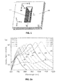
FIG. 1 illustrates a schematic diagram of a single short nanoslit according to embodiments of the present invention with a width W and a length L perforated on a gold film of thickness H. The vertex angle of the cavity is 70.5°, made by Si anisotropic etching. -
FIG. 2A illustrates Electric field intensity E2 spectra of the nanoslit according to embodiments of the invention with a fixed width of 10 nm but with various lengths. -
FIG. 2B illustrates a plot of λSPP/2 at the resonance wavelengths determined inFIG. 2A versus the corresponding length of the rectangular nanoslit (pore) according to embodiments of the present invention. -
FIG. 3 illustrates (a) the calculated SPP mode in the nanoslit (pore) according to embodiments of the invention for a free-space wavelength of 785 nm and (b) the Electric field intensity E2 top view profile (xz-view) inside the nanoslit (pore) (W = 10 nm, L = 90 nm) under illumination at 785 nm according to embodiments of the invention. -
FIG. 4 illustrates scanning electron miscroscopy images of a Fabry-Pérot nanopore (10nm x 100nm) without any Raman analyte (FIG. 4 picture a) and of a long nanoslit (10nm x 6000nm) with five carbonaceous beads as the Raman analyte (FIG. 4 picture b), comparing an embodiment according to the present invention with a long nanoslit. -
FIG. 5 illustrates SERS spectra for a Fabry-Pérot nanopore according to an embodiment of the present invention and a long nanoslit. - The drawings are only schematic and are non-limiting. In the drawings, the size of some of the elements may be exaggerated and not drawn on scale for illustrative purposes.
- Any reference signs in the claims shall not be construed as limiting the scope.
- The present invention will be described with respect to particular embodiments and with reference to certain drawings but the invention is not limited thereto but only by the claims. The drawings described are only schematic and are non-limiting. In the drawings, the size of some of the elements may be exaggerated and not drawn on scale for illustrative purposes. The dimensions and the relative dimensions do not correspond to actual reductions to practice of the invention.
- Furthermore, the terms first, second and the like in the description and in the claims, are used for distinguishing between similar elements and not necessarily for describing a sequence, either temporally, spatially, in ranking or in any other manner. It is to be understood that the terms so used are interchangeable under appropriate circumstances and that the embodiments of the invention described herein are capable of operation in other sequences than described or illustrated herein.
- Moreover, the terms top, under and the like in the description and the claims are used for descriptive purposes and not necessarily for describing relative positions. It is to be understood that the terms so used are interchangeable under appropriate circumstances and that the embodiments of the invention described herein are capable of operation in other orientations than described or illustrated herein.
- It is to be noticed that the term "comprising", used in the claims, should not be interpreted as being restricted to the means listed thereafter; it does not exclude other elements or steps. It is thus to be interpreted as specifying the presence of the stated features, integers, steps or components as referred to, but does not preclude the presence or addition of one or more other features, integers, steps or components, or groups thereof. Thus, the scope of the expression "a device comprising means A and B" should not be limited to devices consisting only of components A and B. It means that with respect to the present invention, the only relevant components of the device are A and B.
- Reference throughout this specification to "one embodiment" or "an embodiment" means that a particular feature, structure or characteristic described in connection with the embodiment is included in at least one embodiment of the present invention. Thus, appearances of the phrases "in one embodiment" or "in an embodiment" in various places throughout this specification are not necessarily all referring to the same embodiment, but may. Furthermore, the particular features, structures or characteristics may be combined in any suitable manner, as would be apparent to one of ordinary skill in the art from this disclosure, in one or more embodiments.
- Similarly it should be appreciated that in the description of exemplary embodiments of the invention, various features of the invention are sometimes grouped together in a single embodiment, figure, or description thereof for the purpose of streamlining the disclosure and aiding in the understanding of one or more of the various inventive aspects. This method of disclosure, however, is not to be interpreted as reflecting an intention that the claimed invention requires more features than are expressly recited in each claim. Rather, as the following claims reflect, inventive aspects lie in less than all features of a single foregoing disclosed embodiment. Thus, the claims following the detailed description are hereby expressly incorporated into this detailed description, with each claim standing on its own as a separate embodiment of this invention.
- Furthermore, while some embodiments described herein include some but not other features included in other embodiments, combinations of features of different embodiments are meant to be within the scope of the invention, and form different embodiments, as would be understood by those in the art. For example, in the following claims, any of the claimed embodiments can be used in any combination.
- In the description provided herein, numerous specific details are set forth. However, it is understood that embodiments of the invention may be practiced without these specific details. In other instances, well-known methods, structures and techniques have not been shown in detail in order not to obscure an understanding of this description.
- Where in embodiments of the present invention reference is made to a sample property, the latter may be a presence or location of an analyte in the sample or a chemical or physical characteristic of the sample or an analyte thereof.
- Where in embodiments of the present invention reference is made to a window, reference is made to an opening or pore extending through a substrate, i.e. from a front side to a back side thereof.
- Where in embodiments of the present invention reference is made to a nanopore, reference is made to a nanosized opening. According to embodiments of the present invention each dimension of the nanosized opening may be sufficiently small so that they do not induce the same effect as would be obtained when the dimension would be infinite.
- In a first aspect according to the present invention, a system is provided for optically determining a sample property using radiation at a predetermined wavelength or in a predetermined wavelength range or for assisting therein. Such a system may be especially suitable for surface enhanced Raman spectroscopy (SERS), surface plasmon resonance measurements, detection of presence of an analyte in a sample or trapping of a particle in a sample. Optical determination may be spectrometric determination. The system according to embodiments of the present invention comprises a nanopore suitable for excitation of plasmons. The nanopore thereby provides a window through the substrate. The window has a smallest window opening of the window has an average length (L) and an average width (W) both being substantially smaller than 2 µm. Typically, the average length and average width both are smaller than twice the smallest free-space wavelength of the wavelength or wavelength range used for optically determining a sample property. By way of illustration, embodiments of the present invention not being limited thereto, an example of a nanopore that could be used is shown in
FIG. 1. FIG. 1 illustrates asubstrate 200 having ananopore 210 providing a window through thesubstrate 200. The average length (L) and the average width (W) of the smallest window size in the nanopore, also referenced as the average length (L) and the average width (W) of the nanopore, also are indicated inFIG. 1 . The nanopore and/or the window created thereby may be substantially rectangular in shape. The average length L and the average width W thereby may be selected so that the nanopore acts along its length as a Fabry-Pérot resonator. Some or all of the walls of the nanopore may be metallic. The nanopore may act as a waveguide resonator supporting a surface Plasmon polariton having a wavelength λSPP function of the average length (L) of the nanopore. The length and width of the Fabry-Pérot may be optimized to enhance the signal intensity at a certain wavelength, e.g. for an excitation wavelength, e.g. for a 785 nm laser to perform Raman experiments. The Fabry-Pérot nanopore cavity according to embodiments of the present invention may also be referred to as a "3D nanoslit" because it is having a significant shorter lengths compared to state of the art referred "2D nanoslits" having a long length, which may with respect to the other lengths be considered as an infinite length. The average width W may be large, e.g. more than 5nm, e.g. more than 7nm, e.g. around 10nm. This is substantially more wide than state of the art nanoslits used for excitation of plasmons. The use of such a width has several advantages. On the one hand, the nanopores according to embodiments of the present invention become suitable for efficiently translocation of relatively large molecules, such as for example relative large biomolecules like proteins. On the other hand, nanopores having a width as described above in combination with a length as described above, are accurately manufacturable using semiconductor manufacturing techniques according to the state of the art. The ratio of the average length (L) to the average width (W) may be smaller than 100. The ratio of length to width may be adapted so that Fabry-Perot resonance conditions are met. According to embodiments of the present invention, the system also may comprise a detector configured with respect to said nanopore for detecting an optical signal, e.g. a Surface Enhanced Raman Spectroscopy signal or a surface Plasmon resonance signal. The system furthermore may comprise a radiation source for providing the radiation at a predetermined wavelength or in a predetermined wavelength range, configured with respect to the nanopore for excitation of plasmons at the nanopore. The system also may comprise an analyser or analyzing means for analyzing a detected optical signal and deriving therefrom a property of the sample. Such an analyzing means may depend on the particular technique used. Further optional features according to embodiments of the present invention and advantages may be as illustrated in the examples. It was surprisingly found that very high enhancement of the field intensity can be obtained. For example, using the rectangular Fabry-Perot (F-P) nanopore-cavity, it is possible to boost thefield intensity 100 times higher than the (long) state of the art long nanoslit-cavity devices which can already enhance the field intensity by a factor of around 300 compared to conventional SERS measurements. This means that e.g. to perform Raman Scattering Analysis, the enhancement factor is almost 10000 times higher. - In one aspect, the present invention also relates to the use of a system as described above, for performing any of a surface enhanced Raman spectroscopy measurement, a surface Plasmon resonance measurement, detecting a presence of a particle in a sample or trapping a particle. It thereby is an advantage that use can be made of translocation of particles, even of relative large particles, such as for example proteins.
- In another aspect, the present invention also relates to a method for determining a sample property using radiation at a predetermined wavelength or in a predetermined wavelength range. The method may be especially suitable for surface enhanced raman spectroscopy or scattering, surface Plasmon resonance detection techniques, optical detection of analytes in samples, optical trapping of particles, etc. The method according to embodiments of the present invention comprises providing interaction between a sample and a substrate comprising a nanopore providing a window through the substrate, whereby a smallest window opening of the window has an average length (L) and an average width (W) both being substantially smaller than 2 µm, irradiating the nanopore so as to excite plasmons at the nanopore, and detecting an optical signal at the nanopore and deriving therefrom a property of the sample. In some embodiments detection may be performed of a shift in resonance wavelength, which may be an indication of the presence of a particle or analyte. In one embodiment, the present invention thus relates to a method wherein detecting an optical signal comprises detecting a shift in an optical resonance frequency of an optical signal at the nanopore and deriving therefrom a presence of an analyte in a sample. More particularly, if the nanopore acts as a Fabry-Pérot resonator, there is a very narrow resonance wavelength, which can be further tuned by the geometrical parameters like length and width. As the Fabry-Pérot resonator is very sensitive to the dielectric constant inside the pore, the presence of analyte molecules can also be detected by checking the slightly shift of the resonance wavelength. In this way embodiments of the present invention also provide a new biosensing principle and a new biosensor. The method may advantageously make use of a system as described above.
- By way of illustration, embodiments of the present invention not being limited thereby, a number of simulation results are provided illustrating features and advantages of embodiments of the present invention. In order to evaluate the electromagnetic field enhancement factors that can be achieved, simulations were performed for rectangular nanopore cavities with a geometry according to embodiments of the present invention. The numerical simulations were 3D finite difference time domain (FDTD) simulations for calculating Maxwell's equations for the complex geometry of a rectangular nanopore-cavity. Here, Lumerical FDTD Solutions software (from Lumerical Solutions, Inc, Canada) was used, allowing visualization of the electromagnetic fields supported by the structures and to study the enhanced electric field intensity E2 inside the nanoslit (pore) and the resonance wavelength λ res of sub-wavelength transmission through the nanoslit (pore). To study the plasmonic properties of nanopores with different lengths, a 3D situation (as shown in
Fig. 1 ) was assumed. The nanoslit (pore) was carved in an 800 nm Au film (height H or thickness of the nanoslit), having a fixed width W at the bottom of the pore of 10 nm and various lengths L ranging from 50 nm to 150 nm. To avoid numerical artefacts related to sharp edges, the edges of the nanopore were rounded according to the experimental situation. The tilted angle of the four sides of the cavity was about 55°, corresponding to the angle induced by anisotropic etching of silicon. Although experimentally the Au film is deposited on top of Si, for the case of simplicity, it is assumed that the entire structure is gold. For sufficiently thick Au films, this assumption does not change the conclusions of the simulation. The whole structure was then immersed in water. Perfectly matched layers (PML) were used as the radiation boundary condition. The PML boundaries in light propagation direction were placed 1 µm away from the structure while in other directions were 500 nm away from the structure. The Au layer penetrated through the PML boundaries. A broadband planar source spanning a wavelength range between 600 nm and 1200 nm, was placed above the whole structure. The mesh grid sizes were set to 0.5 nm in the x-axis, 1-2 nm in the y-axis, and 1 nm in the z-axis (as shown inFig. 1 ). The permittivity data for Au and water were obtained from literature. - The field intensity spectrum was monitored inside the nanopore, at the maximum enhanced location, while the field (xz) profile was monitored at the middle of the nanopore. The transmission spectrum was obtained by integrating the transmitted light 100 nm below the nanopore. Simultaneously the reflection spectrum was monitored.
- For infinitely long nanoslits, it is well known that there is no cut-off for transmission for light polarized perpendicular to the slit (using a similar reference coordinate system as shown in
Fig. 1 ). For a nanopore with all its dimensions well below the free space wavelength, cut-off can be expected. Nevertheless, the gold nanopore supports a highly confined SPP waveguide mode, similar to the mode in a metal-insulator-metal (MIM) plasmon waveguide. This mode has a large effective index, enabling resonance conditions even for very small sizes. Generally, the resonance condition depends on the width and the length of the nanopore and the dielectric constant inside the nanopore. The nanopore-cavity was studied in water, as this kind of devices is typically used in aqueous environment for molecular detection or manipulation. The presence of water already shifts the resonance to longer wavelengths compared to air. In 2D simulations on nanoslit-cavities in air, the resonance is very broad. The enhancement mainly depends on the width of the nanoslit. A smaller gap has stronger electrostatic interaction (SPP coupling) and exhibits a stronger field enhancement. In water, as shown inFig. 2 , the field intensity for the long nanoslit (2D) was similar with the work done by Chen et al before. -
Figure 2(a) shows the numerically evaluated maximum field enhancement inside the nanopore for different lengths and the field enhancement in the nanoslit (2D, corresponding with an infinitely long nanoslit). The lengths tested for the nanopores varied from 50 to 150nm. The reflection and transmission spectra (not shown here) exhibit a similar behaviour of resonance wavelengths. Clear and strong resonances were observed, with a field intensity enhancement exceeding the 2D situation with two orders of magnitude. Moreover, the resonance position strongly depends on the length of the pore, consistent with a Fabry-Pérot resonance picture. In order to investigate this hypothesis, the integrated mode solver of Lumerical FDTD was used to calculate the 2D nanopore SPP mode (xy) profile. An example SPP mode profile at 785 nm, shown inFig. 3(a) , is highly localized near the edges of the nanopore. The white arrows give the direction of increasing signal intensity This is reflected as well in the very high mode index, which is near 3 for most of the investigated free space wavelengths. Based on the effective index of the SPP mode, we can calculate the resonance condition of the rectangular nanopore. For a first order odd Fabry-Pérot resonance mode, it is expected that 2Lres (2π/λSPP) + 2φ = 2π, with Lres the length of the slit at the resonance wavelength, XSPP the wavelength of SPP mode inside the nanopore and φ the phase pick-up upon reflections at the end of the nanopore. For φ = 0, the resonance condition is fulfilled when Lres/λSPP/2. Therefore, as the phase pick up is not known, for the different lengths and their corresponding free-space resonance wavelengths in the transmission spectra, XSPP/2 is calculated and plotted versus the real length inFig. 2(b) . There is a clear linear relation between Lres and XSPP/2. From the slope of the curve, we can deduce the phase pick-up at the edges of the rectangular nanopore, and estimate it to be about n/2, in good agreement with other plasmonic resonators. Detailed investigations of the field profile along the nanopore (as shown inFig. 3(b) ) indeed indicate a λspp/2 resonance, with the field going to zero near the ends of the nanoslit. This is expected since the cavity is truncated by metal. InFIG. 3(b) the white arrows indicate the direction of increasing signal strength. - The above described results and simulations illustrate that he Fabry-Pérot resonance obtained by the nanoslit of the current invention can result in both a clearly narrowed resonance condition and a strongly enhanced field at the resonance wavelength compared to the 2D situation. In the long (state of the art) nanoslits, the enhancement was optimized by either reducing the size of the gap or adding reflective gratings next to the slit. However, fabricating nanoslits with dimensions reproducibly below 10 nm is still challenging. Using the much shorter nanoslit of the present invention makes it possible to obtain resonance conditions which strongly enhance the energy in the nanoslit (nanopore) and correspondingly create a strong field enhancement. Controlling the length of the nanoslit in combination with the width of the nanoslit and the thickness of the substrate in which the slit is made according to the invention allows tuning the resonance to the correct wavelength. For instance, a 785 nm laser is commonly used in SERS. Simultaneously one can take advantage of the clearly defined and narrow resonance for local surface plasmon resonance purposes or plasmonic force trapping within the rectangular nanoslit of the present invention.
- Numerical calculations (as explained above) illustrate that the plasmonic properties of the rectangular nanoslits according to the present invention can be significantly enhanced with varying lengths. It is observed that Fabry-Pérot resonances of highly confined SPP modes in the nanoslits are leading to strong field enhancements in the nanoslit (gap) and are greatly exceeding the case of the infinitely long state of the art nanoslits. An enhancement factor of the field intensity of 104 is obtained even in a 10 nm nanoslit (pore) at λres. Due to the narrow bandwidth of the resonance near λres, the device of the present invention shows a high selectivity to the incident beams. Simultaneously, the λres of the nanoslit (pore) pore can also be tuned easily by simply changing the length of the nanoslit.
- Further by way of illustration, embodiments of the present invention not being limited thereto, experimental results illustrating features and advantages are further discussed. The experimental results illustrate SERS results obtained for a Fabry-Pérot nanopore according to embodiments of the present invention compared with a long nanoslit, indicating surprisingly high efficiency for the Fabry-Pérot nanopore.
FIG. 4 illustrates scanning electron microscopy images of the Fabry-Pérot nanopore according to an embodiment of the present invention (FIG. 4 , picture a) and of a long nanoslit (FIG. 4 , picture b). The Fabry-Pérot nanopore has a size of 10nm x 100nm and has been shown without any Raman analyte being present. The long nanoslit has a size of 10nm x 6000nm and has been shown with five carbonaceous beads present as the Raman analyte. - In
FIG. 5 , the SERS spectra are shown for the Fabry-Pérot nanopore (spectrum 502) and for the long nanoslit (spectrum 504). The SERS spectra are recorded using an excitation laser having a wavelength of 633nm and an intensity of about 0.1 W/µm2. The intensity of the Raman spectra are normalized by the integration time and the amount of bead, for allowing appropriate comparison between the nanopore and nanoslit results. Carbonaceous nanoparticles are used as Raman analytes, whereby for the nanopore one bead is used and for the nanoslit five beads are used. The size of the beads is about 20nm and the beads are deposited by electron beam induced deposition. The integration time used for measuring of the SERS spectra is 10s and 2s for the nanoslit and the nanopore respectively. - The normalized spectra indicate a surprisingly high intensity difference for the nanoslit and for the nanopore. It can be seen that the SERS intensity is more than a
factor 100 higher when using a nanopore compared to the situation using a nanoslit, resulting in the nanopores being especially advantageous for SERS.
Claims (15)
- A system for assisting in optically determining a sample property using radiation at a predetermined wavelength or in a predetermined wavelength range, the system comprising
a substrate (200) comprising a nanopore (210) for excitation of plasmons, the nanopore (210) providing a window through the substrate, whereby a smallest window opening of the window has an average length (L) and an average width (W) both being substantially smaller than 2 µm. - A system according to claim 1, wherein the average length of the window opening is determined as function of the average wavelength of the radiation used and the effective refractive index at the nanopore (210).
- A system according to any of claims 1 or 2, the average length (L) and the average width (W) of the nanopore (210) being selected so that the nanopore (210) acts along its length as a Fabry-Pérot resonator.
- A system according to claim 3, wherein the nanopore (210) is a waveguide resonator supporting a surface Plasmon polariton having a wavelength λSPP function of the average length (L) of the nanopore (210).
- A system according to any of the previous claims, wherein the ratio of the average length (L) to the average width (W) is smaller than 100.
- A system according to any of the previous claims, wherein the average width (W) of the nanopore (210) is at least 5nm.
- A system according to any of the previous claims, wherein the walls of the nanopore (210) are metallic.
- A system according to any of the previous claims, the system furthermore comprising a detector configured with respect to said nanopore (210) for detecting an optical signal at the nanopore (210).
- A system according to any of the previous claims, the system furthermore comprising a radiation source for providing radiation at a predetermined wavelength or in a predetermined wavelength range, configured with respect to the nanopore (210) for excitation of plasmons at the nanopore (210).
- Use of a system according to any of claims 1 to 9, for performing any of a surface enhanced Raman spectroscopy measurement, a surface Plasmon resonance measurement, detecting a presence of a particle in a sample or trapping a particle.
- A method for optically determining a sample property using radiation at a predetermined wavelength or in a predetermined wavelength range, the method comprising- providing interaction between a sample and a substrate (200) comprising a nanopore (210) providing a window through the substrate (200), whereby a smallest window opening of the window has an average length (L) and an average width (W) both being substantially smaller than 2 µm,- irradiating the nanopore (210) so as to excite plasmons at the nanopore (210), and- detecting an optical signal at the nanopore (210) and deriving therefrom a property of the sample.
- A method according to claim 11, wherein providing interaction between a sample and a substrate (200) comprises providing interaction between a sample and a substrate (200) of a system according to any of claims 1 to 9.
- A method according to any of claims 11 to 12, wherein detecting an optical signal comprises detecting a surface enhanced Raman spectroscopy response or a surface Plasmon resonance response.
- A method according to any of claims 11 to 13, wherein detecting an optical signal comprises detecting a shift in an optical resonance frequency of an optical signal at the nanopore (210) and deriving therefrom a presence of an analyte in a sample.
- A method according to any of claims 11 to 14, wherein providing interaction between a sample and a substrate (200) comprises translocating proteins in the sample through the window in the substrate (200).
Applications Claiming Priority (1)
| Application Number | Priority Date | Filing Date | Title |
|---|---|---|---|
| US36130410P | 2010-07-02 | 2010-07-02 |
Publications (2)
| Publication Number | Publication Date |
|---|---|
| EP2402738A2 true EP2402738A2 (en) | 2012-01-04 |
| EP2402738A3 EP2402738A3 (en) | 2012-01-11 |
Family
ID=44675029
Family Applications (1)
| Application Number | Title | Priority Date | Filing Date |
|---|---|---|---|
| EP11172296A Withdrawn EP2402738A3 (en) | 2010-07-02 | 2011-06-30 | Spectroscopy using nanopore cavities |
Country Status (2)
| Country | Link |
|---|---|
| US (1) | US8928867B2 (en) |
| EP (1) | EP2402738A3 (en) |
Cited By (1)
| Publication number | Priority date | Publication date | Assignee | Title |
|---|---|---|---|---|
| CN102590940A (en) * | 2012-03-06 | 2012-07-18 | 北京航空航天大学 | Open type surface plasmon polariton slit optical waveguide |
Families Citing this family (6)
| Publication number | Priority date | Publication date | Assignee | Title |
|---|---|---|---|---|
| US20120006981A1 (en) * | 2009-03-31 | 2012-01-12 | Imec | Waveguide integrated photodetector |
| GB201212135D0 (en) | 2012-07-09 | 2012-08-22 | Base4 Innovation Ltd | Improved sequencing apparatus |
| DE102014205660B4 (en) * | 2014-03-26 | 2020-02-13 | Bundesrepublik Deutschland, vertr. durch das Bundesministerium für Wirtschaft und Energie, dieses vertreten durch den Präsidenten der Physikalisch-Technischen Bundesanstalt | Test specimen for the calibration of a Raman microscope |
| US10908144B2 (en) * | 2017-05-09 | 2021-02-02 | Stanley Kent Kemmish, JR. | Stacks of coaligned nanopores and fabrication and uses thereof |
| CN108493527B (en) * | 2018-05-09 | 2020-12-15 | 桂林电子科技大学 | A rectangular cavity plasmonic filter embedded in a MIM waveguide |
| CN115873932A (en) * | 2021-08-11 | 2023-03-31 | 上海近观科技有限责任公司 | Plasmon optical enhancement chip system and application thereof |
Family Cites Families (5)
| Publication number | Priority date | Publication date | Assignee | Title |
|---|---|---|---|---|
| US7892489B2 (en) * | 2003-05-27 | 2011-02-22 | Optotrace Technologies, Inc. | Light scattering device having multi-layer micro structure |
| EP1784678A2 (en) * | 2004-08-19 | 2007-05-16 | University of Pittsburgh | Chip-scale optical spectrum analyzers with enhanced resolution |
| GB2419940B (en) * | 2004-11-04 | 2007-03-07 | Mesophotonics Ltd | Metal nano-void photonic crystal for enhanced raman spectroscopy |
| GB0717150D0 (en) * | 2007-09-04 | 2007-10-17 | Univ Warwick | Apparatus and method |
| EP2196796A1 (en) * | 2008-12-09 | 2010-06-16 | Imec | Single molecule optical spectroscopy in solid-state nanopores in a transmission-based approach |
-
2011
- 2011-06-30 EP EP11172296A patent/EP2402738A3/en not_active Withdrawn
- 2011-07-05 US US13/176,359 patent/US8928867B2/en not_active Expired - Fee Related
Non-Patent Citations (9)
| Title |
|---|
| ALEXANDRE G. BROLO ET AL: "Nanohole-Enhanced Raman Scattering", NANO LETTERS, vol. 4, no. 10, 1 October 2004 (2004-10-01), pages 2015 - 2018, XP055078602, ISSN: 1530-6984, DOI: 10.1021/nl048818w * |
| CHANG CHEN ET AL: "Direct Evidence of High Spatial Localization of Hot Spots in Surface-Enhanced Raman Scattering", ANGEWANDTE CHEMIE INTERNATIONAL EDITION, vol. 48, no. 52, 21 December 2009 (2009-12-21), pages 9932 - 9935, XP055195109, ISSN: 1433-7851, DOI: 10.1002/anie.200905389 * |
| CHANG CHEN ET AL: "Highly confined surface plasmon polariton resonances in rectangular nanopore cavities", PHYSICA STATUS SOLIDI (RRL) - RAPID RESEARCH LETTERS, vol. 4, no. 10, 1 October 2010 (2010-10-01), pages 247 - 249, XP055012756, ISSN: 1862-6254, DOI: 10.1002/pssr.201004268 * |
| CHANG CHEN: "PLASMONIC NANOPORES FOR DIRECT MOLECULAR IDENTIFICATION", 1 May 2011 (2011-05-01), Leuven, XP055266571, Retrieved from the Internet <URL:https://lirias.kuleuven.be/1722728?limo=0> [retrieved on 20160419] * |
| EDWARD S BARNARD ET AL: "Spectral properties of plasmonic resonator antennasOptical properties of metallic films for vertical- cavity optoelectronic devices", PHYS. REV. LETT. NAT. PHOTON. PHYS. REV. LET. PHYS. REV. LETT. OPT. LETT. PHYS. REV. LETT. OPT. LETT. PHYS. REV. B. MATER. TODAY NANO LETT. PHYS. REV. LETT. PHYS. STATUS SOLIDI B PHYS. REV. LETT. SCIENCE OPT. EXPRESS E. N. ECONOMOU PHYS. REV. PHYS. R, 1 January 2007 (2007-01-01), pages 641 - 648, XP055265993, Retrieved from the Internet <URL:https://www.osapublishing.org/DirectPDFAccess/04665E4D-F0E8-D67B-AD0E7F010C324A8F_172466/oe-16-21-16529.pdf?da=1&id=172466&seq=0&mobile=no> * |
| EDWARD S BARNARD ET AL: "Spectral properties of plasmonic resonator antennasOptical properties of metallic films for vertical- cavity optoelectronic devices", PHYS. REV. LETT. NAT. PHOTON. PHYS. REV. LET. PHYS. REV. LETT. OPT. LETT. PHYS. REV. LETT. OPT. LETT. PHYS. REV. B. MATER. TODAY NANO LETT. PHYS. REV. LETT. PHYS. STATUS SOLIDI B PHYS. REV. LETT. SCIENCE OPT. EXPRESS E. N. ECONOMOU PHYS. REV. PHYS. R, 1 January 2007 (2007-01-01), pages 641 - 648, XP055265996, Retrieved from the Internet <URL:https://www.osapublishing.org/DirectPDFAccess/04665E4D-F0E8-D67B-AD0E7F010C324A8F_172466/oe-16-21-16529.pdf?da=1&id=172466&seq=0&mobile=no> * |
| GRACE M HWANG ET AL: "Plasmonic Sensing of Biological Analytes Through Nanoholes", IEEE SENSORS JOURNAL, IEEE SERVICE CENTER, NEW YORK, NY, US, vol. 8, no. 12, 1 December 2008 (2008-12-01), pages 2074 - 2079, XP011238232, ISSN: 1530-437X, DOI: 10.1109/JSEN.2008.2007663 * |
| MATHILDE GAVILLET ET AL: "Flow cytometric assay for direct quantification of neutrophil extracellular traps in blood samples", AMERICAN JOURNAL OF HEMATOLOGY, vol. 90, no. 12, 1 December 2015 (2015-12-01), US, pages 1155 - 1158, XP055266054, ISSN: 0361-8609, DOI: 10.1002/ajh.24185 * |
| R. GORDON ET AL: "Resonant light transmission through a nanohole in a metal film", IEEE TRANSACTIONS ON NANOTECHNOLOGY, vol. 5, no. 3, 1 May 2006 (2006-05-01), pages 291 - 294, XP055194935, ISSN: 1536-125X, DOI: 10.1109/TNANO.2006.874057 * |
Cited By (2)
| Publication number | Priority date | Publication date | Assignee | Title |
|---|---|---|---|---|
| CN102590940A (en) * | 2012-03-06 | 2012-07-18 | 北京航空航天大学 | Open type surface plasmon polariton slit optical waveguide |
| CN102590940B (en) * | 2012-03-06 | 2013-09-18 | 北京航空航天大学 | Open type surface plasmon polariton slit optical waveguide |
Also Published As
| Publication number | Publication date |
|---|---|
| US8928867B2 (en) | 2015-01-06 |
| EP2402738A3 (en) | 2012-01-11 |
| US20120170034A1 (en) | 2012-07-05 |
Similar Documents
| Publication | Publication Date | Title |
|---|---|---|
| US8928867B2 (en) | Spectroscopy using nanopore cavities | |
| EP3028033B1 (en) | Optical sensor based on multilayered plasmonic structure comprising a nanoporous metallic layer | |
| US8687187B2 (en) | Surface enhanced raman spectroscopy on optical resonator (e.g., photonic crystal) surfaces | |
| US10725373B1 (en) | Nano-patterning methods including: (1) patterning of nanophotonic structures at optical fiber tip for refractive index sensing and (2) plasmonic crystal incorporating graphene oxide gas sensor for detection of volatile organic compounds | |
| Liang et al. | Subradiant dipolar interactions in plasmonic nanoring resonator array for integrated label-free biosensing | |
| US10801956B2 (en) | Resonant periodic structures and methods of using them as filters and sensors | |
| US20140322081A1 (en) | Sensing devices and techniques using 3-d arrays based on surface plasmon excitations | |
| Li et al. | $ L_ {n} $ slot photonic crystal microcavity for refractive index gas sensing | |
| JP2012132886A (en) | Method and device for measuring optical characteristics of dielectric on metal thin film | |
| CN104007098B (en) | Resonant mirror strengthens Raman spectrum detecting device | |
| JP2019522184A (en) | Particle characterization in an open optical resonant cavity | |
| Yang et al. | Synthesis of multifunctional plasmonic nanopillar array using soft thermal nanoimprint lithography for highly sensitive refractive index sensing | |
| Adhikari et al. | A voyage from plasmonic to hybrid waveguide refractive index sensors based on wavelength interrogation technique: a review | |
| Gaur et al. | Plasmonic refractive index sensor based on metal insulator metal waveguide | |
| Galli et al. | Single-mode versus multimode behavior in silicon photonic crystal waveguides measured by attenuated total reflectance | |
| Beermann et al. | Field enhancement and extraordinary optical transmission by tapered periodic slits in gold films | |
| Canpean et al. | Multifunctional plasmonic sensors on low-cost subwavelength metallic nanoholes arrays | |
| Jin et al. | Large-area nanogap plasmon resonator arrays for plasmonics applications | |
| Soehartono et al. | Ultra-small v-shaped gold split ring resonators for biosensing using fundamental magnetic resonance in the visible spectrum | |
| Wong et al. | Theory of hyperbolic stratified nanostructures for surface-enhanced Raman scattering | |
| JP2012098211A (en) | Optical characteristic of metal thin film measurement device and optical characteristic of metal thin film measurement method | |
| Sanders et al. | Lattice resonances of nanohole arrays for quantum enhanced sensing | |
| Wang et al. | Ultracompact Refractive Index Sensor Based on Surface-Plasmon-Polariton Interference | |
| Chang et al. | Surface-enhanced infrared absorption-based CO 2 sensor using photonic crystal slab | |
| Kan et al. | Long-range surface plasmon resonance sensor with liquid micro-channels to maintain the symmetry condition of the refractive index |
Legal Events
| Date | Code | Title | Description |
|---|---|---|---|
| PUAL | Search report despatched |
Free format text: ORIGINAL CODE: 0009013 |
|
| AK | Designated contracting states |
Kind code of ref document: A2 Designated state(s): AL AT BE BG CH CY CZ DE DK EE ES FI FR GB GR HR HU IE IS IT LI LT LU LV MC MK MT NL NO PL PT RO RS SE SI SK SM TR |
|
| AX | Request for extension of the european patent |
Extension state: BA ME |
|
| PUAI | Public reference made under article 153(3) epc to a published international application that has entered the european phase |
Free format text: ORIGINAL CODE: 0009012 |
|
| AK | Designated contracting states |
Kind code of ref document: A3 Designated state(s): AL AT BE BG CH CY CZ DE DK EE ES FI FR GB GR HR HU IE IS IT LI LT LU LV MC MK MT NL NO PL PT RO RS SE SI SK SM TR |
|
| AX | Request for extension of the european patent |
Extension state: BA ME |
|
| RIC1 | Information provided on ipc code assigned before grant |
Ipc: G01N 21/55 20060101ALI20111205BHEP Ipc: G01N 21/65 20060101AFI20111205BHEP |
|
| 17P | Request for examination filed |
Effective date: 20120710 |
|
| 17Q | First examination report despatched |
Effective date: 20150625 |
|
| RAP1 | Party data changed (applicant data changed or rights of an application transferred) |
Owner name: IMEC VZW Owner name: KATHOLIEKE UNIVERSITEIT LEUVEN K.U. LEUVEN R&D |
|
| STAA | Information on the status of an ep patent application or granted ep patent |
Free format text: STATUS: THE APPLICATION HAS BEEN WITHDRAWN |
|
| 18W | Application withdrawn |
Effective date: 20191111 |