EP2402152A1 - Metal-clad polyimide resin substrate with excellent thermal aging resistance characteristics - Google Patents
Metal-clad polyimide resin substrate with excellent thermal aging resistance characteristics Download PDFInfo
- Publication number
- EP2402152A1 EP2402152A1 EP10746117A EP10746117A EP2402152A1 EP 2402152 A1 EP2402152 A1 EP 2402152A1 EP 10746117 A EP10746117 A EP 10746117A EP 10746117 A EP10746117 A EP 10746117A EP 2402152 A1 EP2402152 A1 EP 2402152A1
- Authority
- EP
- European Patent Office
- Prior art keywords
- layer
- metal
- polyimide resin
- peel strength
- resin substrate
- Prior art date
- Legal status (The legal status is an assumption and is not a legal conclusion. Google has not performed a legal analysis and makes no representation as to the accuracy of the status listed.)
- Withdrawn
Links
Images
Classifications
-
- B—PERFORMING OPERATIONS; TRANSPORTING
- B32—LAYERED PRODUCTS
- B32B—LAYERED PRODUCTS, i.e. PRODUCTS BUILT-UP OF STRATA OF FLAT OR NON-FLAT, e.g. CELLULAR OR HONEYCOMB, FORM
- B32B15/00—Layered products comprising a layer of metal
- B32B15/04—Layered products comprising a layer of metal comprising metal as the main or only constituent of a layer, which is next to another layer of the same or of a different material
- B32B15/08—Layered products comprising a layer of metal comprising metal as the main or only constituent of a layer, which is next to another layer of the same or of a different material of synthetic resin
- B32B15/088—Layered products comprising a layer of metal comprising metal as the main or only constituent of a layer, which is next to another layer of the same or of a different material of synthetic resin comprising polyamides
-
- B—PERFORMING OPERATIONS; TRANSPORTING
- B32—LAYERED PRODUCTS
- B32B—LAYERED PRODUCTS, i.e. PRODUCTS BUILT-UP OF STRATA OF FLAT OR NON-FLAT, e.g. CELLULAR OR HONEYCOMB, FORM
- B32B15/00—Layered products comprising a layer of metal
- B32B15/20—Layered products comprising a layer of metal comprising aluminium or copper
-
- B—PERFORMING OPERATIONS; TRANSPORTING
- B32—LAYERED PRODUCTS
- B32B—LAYERED PRODUCTS, i.e. PRODUCTS BUILT-UP OF STRATA OF FLAT OR NON-FLAT, e.g. CELLULAR OR HONEYCOMB, FORM
- B32B15/00—Layered products comprising a layer of metal
- B32B15/04—Layered products comprising a layer of metal comprising metal as the main or only constituent of a layer, which is next to another layer of the same or of a different material
- B32B15/08—Layered products comprising a layer of metal comprising metal as the main or only constituent of a layer, which is next to another layer of the same or of a different material of synthetic resin
-
- B—PERFORMING OPERATIONS; TRANSPORTING
- B32—LAYERED PRODUCTS
- B32B—LAYERED PRODUCTS, i.e. PRODUCTS BUILT-UP OF STRATA OF FLAT OR NON-FLAT, e.g. CELLULAR OR HONEYCOMB, FORM
- B32B27/00—Layered products comprising a layer of synthetic resin
- B32B27/28—Layered products comprising a layer of synthetic resin comprising synthetic resins not wholly covered by any one of the sub-groups B32B27/30 - B32B27/42
- B32B27/281—Layered products comprising a layer of synthetic resin comprising synthetic resins not wholly covered by any one of the sub-groups B32B27/30 - B32B27/42 comprising polyimides
-
- C—CHEMISTRY; METALLURGY
- C25—ELECTROLYTIC OR ELECTROPHORETIC PROCESSES; APPARATUS THEREFOR
- C25D—PROCESSES FOR THE ELECTROLYTIC OR ELECTROPHORETIC PRODUCTION OF COATINGS; ELECTROFORMING; APPARATUS THEREFOR
- C25D5/00—Electroplating characterised by the process; Pretreatment or after-treatment of workpieces
- C25D5/54—Electroplating of non-metallic surfaces
- C25D5/56—Electroplating of non-metallic surfaces of plastics
-
- H—ELECTRICITY
- H05—ELECTRIC TECHNIQUES NOT OTHERWISE PROVIDED FOR
- H05K—PRINTED CIRCUITS; CASINGS OR CONSTRUCTIONAL DETAILS OF ELECTRIC APPARATUS; MANUFACTURE OF ASSEMBLAGES OF ELECTRICAL COMPONENTS
- H05K3/00—Apparatus or processes for manufacturing printed circuits
- H05K3/38—Improvement of the adhesion between the insulating substrate and the metal
- H05K3/388—Improvement of the adhesion between the insulating substrate and the metal by the use of a metallic or inorganic thin film adhesion layer
-
- B—PERFORMING OPERATIONS; TRANSPORTING
- B32—LAYERED PRODUCTS
- B32B—LAYERED PRODUCTS, i.e. PRODUCTS BUILT-UP OF STRATA OF FLAT OR NON-FLAT, e.g. CELLULAR OR HONEYCOMB, FORM
- B32B2255/00—Coating on the layer surface
- B32B2255/20—Inorganic coating
- B32B2255/205—Metallic coating
-
- B—PERFORMING OPERATIONS; TRANSPORTING
- B32—LAYERED PRODUCTS
- B32B—LAYERED PRODUCTS, i.e. PRODUCTS BUILT-UP OF STRATA OF FLAT OR NON-FLAT, e.g. CELLULAR OR HONEYCOMB, FORM
- B32B2307/00—Properties of the layers or laminate
- B32B2307/20—Properties of the layers or laminate having particular electrical or magnetic properties, e.g. piezoelectric
- B32B2307/202—Conductive
-
- B—PERFORMING OPERATIONS; TRANSPORTING
- B32—LAYERED PRODUCTS
- B32B—LAYERED PRODUCTS, i.e. PRODUCTS BUILT-UP OF STRATA OF FLAT OR NON-FLAT, e.g. CELLULAR OR HONEYCOMB, FORM
- B32B2307/00—Properties of the layers or laminate
- B32B2307/50—Properties of the layers or laminate having particular mechanical properties
- B32B2307/546—Flexural strength; Flexion stiffness
-
- B—PERFORMING OPERATIONS; TRANSPORTING
- B32—LAYERED PRODUCTS
- B32B—LAYERED PRODUCTS, i.e. PRODUCTS BUILT-UP OF STRATA OF FLAT OR NON-FLAT, e.g. CELLULAR OR HONEYCOMB, FORM
- B32B2307/00—Properties of the layers or laminate
- B32B2307/70—Other properties
- B32B2307/732—Dimensional properties
-
- C—CHEMISTRY; METALLURGY
- C25—ELECTROLYTIC OR ELECTROPHORETIC PROCESSES; APPARATUS THEREFOR
- C25D—PROCESSES FOR THE ELECTROLYTIC OR ELECTROPHORETIC PRODUCTION OF COATINGS; ELECTROFORMING; APPARATUS THEREFOR
- C25D5/00—Electroplating characterised by the process; Pretreatment or after-treatment of workpieces
- C25D5/34—Pretreatment of metallic surfaces to be electroplated
-
- H—ELECTRICITY
- H05—ELECTRIC TECHNIQUES NOT OTHERWISE PROVIDED FOR
- H05K—PRINTED CIRCUITS; CASINGS OR CONSTRUCTIONAL DETAILS OF ELECTRIC APPARATUS; MANUFACTURE OF ASSEMBLAGES OF ELECTRICAL COMPONENTS
- H05K1/00—Printed circuits
- H05K1/02—Details
- H05K1/03—Use of materials for the substrate
- H05K1/0313—Organic insulating material
- H05K1/032—Organic insulating material consisting of one material
- H05K1/0346—Organic insulating material consisting of one material containing N
-
- H—ELECTRICITY
- H05—ELECTRIC TECHNIQUES NOT OTHERWISE PROVIDED FOR
- H05K—PRINTED CIRCUITS; CASINGS OR CONSTRUCTIONAL DETAILS OF ELECTRIC APPARATUS; MANUFACTURE OF ASSEMBLAGES OF ELECTRICAL COMPONENTS
- H05K2201/00—Indexing scheme relating to printed circuits covered by H05K1/00
- H05K2201/01—Dielectrics
- H05K2201/0137—Materials
- H05K2201/0154—Polyimide
-
- H—ELECTRICITY
- H05—ELECTRIC TECHNIQUES NOT OTHERWISE PROVIDED FOR
- H05K—PRINTED CIRCUITS; CASINGS OR CONSTRUCTIONAL DETAILS OF ELECTRIC APPARATUS; MANUFACTURE OF ASSEMBLAGES OF ELECTRICAL COMPONENTS
- H05K3/00—Apparatus or processes for manufacturing printed circuits
- H05K3/38—Improvement of the adhesion between the insulating substrate and the metal
- H05K3/381—Improvement of the adhesion between the insulating substrate and the metal by special treatment of the substrate
-
- Y—GENERAL TAGGING OF NEW TECHNOLOGICAL DEVELOPMENTS; GENERAL TAGGING OF CROSS-SECTIONAL TECHNOLOGIES SPANNING OVER SEVERAL SECTIONS OF THE IPC; TECHNICAL SUBJECTS COVERED BY FORMER USPC CROSS-REFERENCE ART COLLECTIONS [XRACs] AND DIGESTS
- Y10—TECHNICAL SUBJECTS COVERED BY FORMER USPC
- Y10T—TECHNICAL SUBJECTS COVERED BY FORMER US CLASSIFICATION
- Y10T428/00—Stock material or miscellaneous articles
- Y10T428/31504—Composite [nonstructural laminate]
- Y10T428/31678—Of metal
- Y10T428/31681—Next to polyester, polyamide or polyimide [e.g., alkyd, glue, or nylon, etc.]
Definitions
- the present invention relates to an adhesive-free flexible laminate material for use as a mounting material of electronic components such as a flexibly print substrate, TAB and COF, and in particular relates to a metal-coated polyimide resin substrate with excellent thermal aging resistance properties.
- FCCL Flexible Copper Clad Laminate
- metal conductor layers primarily formed from copper are laminated on a polyimide film
- FCCL Flexible Copper Clad Laminate
- an adhesive-free flexible laminate that does not comprise an adhesive layer between a polyimide film and a metal layer is attracting attention pursuant to the demands of finer pitches of the circuit wiring width.
- an adhesive-free flexible laminate in particular an adhesive-free flexible laminate capable of accommodating fine pitches; there is a so-called metalizing method, in which a barrier layer and a seed layer are formed on a polyimide resin film in advance by a dry plating method such as sputtering, CVD or vapor deposition, and a metal layer film as the conductor layer is subsequently deposited by electrolytic plating.
- a dry plating method such as sputtering, CVD or vapor deposition
- a metal layer film as the conductor layer is subsequently deposited by electrolytic plating.
- surface modification is performed for the purpose of improving the adhesiveness with the barrier metal by subjecting the polyimide resin film surface to plasma treatment (refer to Patent Document 1 and Patent Document 2).
- a method of forming a barrier layer and a seed layer on a polyimide resin film in advance by electroless plating, and subsequently depositing a metal layer as a conductor layer by electrolytic plating prior to forming the metal layer, surface modification is performed by immersing the polyimide resin film in a solution made of alkali metal hydroxide in order to improve the adsorption of the catalyst to serve as the drive force of the subsequent electroless plating, and to improve the adhesiveness with the barrier metal (refer to Patent Document 3).
- the surface modification treatment of the polyimide resin film has a major impact on the adhesiveness between the polyimide resin film and the metal layer, and it is a particularly important treatment process in terms of production.
- the initial peel strength and the peel strength after the lapse of a long period are important, and in recent years the long-term peel strength is becoming particularly important as a requirement for high reliability.
- the long-term peel strength is generally evaluated based on peel measurement after thermal aging (at 150°C for 168 hours), which is an accelerated deterioration test.
- Patent Document 1 Japanese Patent No. 3173511
- An object of this invention is to provide a metal-coated polyimide resin substrate that does not deteriorate the initial adhesion between the metal-coated polyimide resin film and the metal layer and has high adhesion after aging at 150°C for 168 hours.
- the present invention provides:
- the present invention additionally provides:
- the present invention is a metal-coated polyimide resin substrate in which a barrier layer is formed by a dry process after performing surface modification to one surface or both surfaces of a polyimide resin film by a dry process, a seed layer is thereafter formed by a wet process or a dry process, and a conductive film is formed on a surface layer thereof by a wet process; and yields superior effects of being able to increase the adhesion after aging without deteriorating the initial adhesion between the polyimide film and the metal layer after lamination.
- a metal-coated polyimide resin substrate is produced by forming a barrier layer after performing surface modification to one surface or both surfaces of a polyimide resin film by a wet process or a dry process, forming a seed layer on the foregoing barrier layer, and additionally forming a conductive film having a given thickness on the foregoing seed layer.
- a dry process such as sputtering, CVD and vapor deposition may be used for forming the barrier layer on the polyimide resin film.
- FCCL Flexible Copper Clad Laminate
- the normal peel strength (initial peel strength) and the thermal peel strength (peel strength after aging at 150°C for 168 hours) as the accelerated deterioration test are generally measured.
- the long-term peel strength is becoming particularly important as a requirement for high reliability, and there are demands for increasing the peel strength retention after an aging test at 150°C for 168 hours (thermal peel strength/normal peel strength) as much as possibly.
- the present inventors conducted intense study regarding the structure of the peeling surface on the metal layer side in the depth direction when the metal-coated polyimide resin substrate was subject to 90-degree peeling. It was discovered thereby there is a mixed layer of the barrier layer (nickel, chromium or its alloy layer) formed after the surface modification treatment and the polyimide. Although this will depend on the modification treatment of the polyimide resin, generally speaking, if the modification treatment is excessive, the incorporation of the barrier layer metal into the polyimide modification layer will increase, and the mixed layer of the barrier layer metal and polyimide will increase.
- the barrier layer nickel, chromium or its alloy layer
- the sputter energy in forming the barrier layer increases, the implantation of the barrier metal into the polyimide layer will increase, and the mixed layer of barrier layer metal and polyimide gets thicker.
- the deterioration in the peel strength after thermal aging was caused by the thickness of the mixed layer of polyimide and barrier layer metal at the initial peeling surface on the metal layer side.
- the copper having a catalytic oxidation effect is more easily dispersed in the polyimide layer through the mixed layer; and therefore, the deterioration in the molecular structure of the polyimide resin is promoted and the peel strength consequently deteriorates in the thermal aging.
- the thickness of the mixed layer of polyimide and metal at the peeling surface on the metal layer side in the initial peel it is possible to maintain the peel strength after thermal aging at a high level, and additionally possible to estimate the peel strength after the thermal aging from the thickness of the mixed layer of polyimide and metal at the initial peeling surface on the metal layer side.
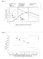
- Fig. 1 is a diagram schematically showing the examination results on the thickness of a mixed layer of the polyimide residue (C-C) and the barrier metal (Ni) layer residue at the peeling surface on the metal layer side according to in-depth profiling with a time-of-flight secondary ion mass spectrometer (TOF-SIMS).
- TOF-SIMS time-of-flight secondary ion mass spectrometer
- the polyimide residue (C-C) reaches its peak in the vicinity of 2 nm as the sputter depth based on Si conversion
- the barrier metal (Ni) reaches its peak in the vicinity of 4.5 nm as the sputter depth based on Si conversion.
- the intermediate thereof is the mixed layer of polyimide and metal.
- the present inventors discovered that the peel strength retention after an aging test at 150°C for 168 hours (thermal peel strength/normal peel strength) will increase when the thickness of a mixed layer of polyimide and barrier layer metal at the peeling surface on the metal layer side according to in-depth profiling with TOF-SIMS is 0.70 nm or less based on Si sputter rate conversion. In the foregoing case, it was possible to achieve peel strength retention of 50% or higher.
- Kapton 150EN manufactured by Du Pont was used as the polyimide resin film.
- This polyimide resin film was subject to plasma treatment, and a barrier layer composed of nickel chromium alloy was formed by sputtering to achieve a thickness of 25.0 nm.
- a seed copper layer was formed by sputtering and a copper conductor layer of 8 ⁇ m was formed by electroplating.
- a sample having the following peel characteristics namely, a normal peel strength of 0.66 kN/m and a thermal peel strength of 0.36 kN/m, was obtained.
- Fig. 2 is a diagram showing the relationship of the peel strength retention (%) relative to the thickness (thickness nm based on Si conversion) of a mixed layer of barrier metal and Pl (polyimide). As shown in Fig.
- the thickness of a mixed layer of barrier metal (Ni) and polyimide was 0.53 nm based on Si conversion, and the peel strength retention (thermal peel strength/normal peel strength) showed favorable results at 55%.
- the foregoing measurement results are shown in Table 1.
- Kapton 150EN manufactured by Du Pont was used as the polyimide resin film.
- This polyimide resin film was subject to plasma treatment, and a barrier layer composed of nickel chromium alloy was formed by sputtering to achieve a thickness of 25.0 nm.
- a seed copper layer was formed by sputtering.
- a copper conductor layer of 8 ⁇ m was formed by electroplating, and the peel strength was measured. Consequently, a sample having the following peel characteristics; namely, a normal peel strength of 0.80 kN/m and a thermal peel strength of 0.48 kN/m, was obtained.
- the thickness of the mixed layer of polyimide and seed layer metal at the peeling surface on the metal layer side in the normal peel was measured according to the in-depth profiling with the time-of-flight secondary ion mass spectrometer (TOF-SIMS).
- TOF-SIMS time-of-flight secondary ion mass spectrometer
- the thickness of a mixed layer of the barrier metal (Ni) and polyimide was 0.41 nm based on Si conversion, and the peel strength retention (thermal peel strength/normal peel strength) showed favorable results at 55%.
- Table 1 The foregoing measurement results are shown in Table 1.
- Kapton 150EN manufactured by Du Pont was used as the polyimide resin film.
- This polyimide resin film was subject to plasma treatment, and a barrier layer composed of nickel chromium alloy was formed by sputtering to achieve a thickness of 25.0 nm.
- a seed copper layer was formed by sputtering.
- a copper conductor layer of 8 ⁇ m was formed by electroplating, and the peel strength was measured. Consequently, a sample having the following peel characteristics; namely, a normal peel strength of 0.79 kN/m and a thermal peel strength of 0.38 kN/m, was obtained.
- the thickness of the mixed layer of polyimide and seed layer metal at the peeling surface on the metal layer side in the normal peel was measured according to the in-depth profiling with the time-of-flight secondary ion mass spectrometer (TOF-SIMS). Consequently, as shown in Fig. 2 , the thickness of a mixed layer of the barrier metal (Ni) and polyimide was 0.77 nm based on Si conversion, and the peel strength retention (thermal peel strength/normal peel strength) was inferior at 48%.
- TOF-SIMS time-of-flight secondary ion mass spectrometer
- Kapton 150EN manufactured by Du Pont was used as the polyimide resin film.
- This polyimide resin film was subject to plasma treatment, and a barrier layer composed of nickel chromium alloy was formed by sputtering to achieve a thickness of 25.0 nm.
- a seed copper layer was formed by sputtering.
- a copper conductor layer of 8 ⁇ m was formed by electroplating, and the peel strength was measure. Consequently, a sample having the following peel characteristics; namely, a normal peel strength of 0.77 kN/m and a thermal peel strength of 0.31 kN/m, was obtained.
- the thickness of the mixed layer of polyimide and seed layer metal at the peeling surface on the metal layer side in the formal peel was measured according to the in-depth profiling with the time-of-flight secondary ion mass spectrometer (TOF-SIMS). Consequently, as shown in Fig. 2 , the thickness of a mixed layer of the barrier metal (Ni) and polyimide was 0.97 nm based on Si conversion, and the peel strength retention (thermal peel strength/normal peel strength) was inferior at 40%.
- TOF-SIMS time-of-flight secondary ion mass spectrometer
- the peel strength retention (thermal peel strength/normal peel strength) tends to deteriorate, and it was confirmed that the thickness of a mixed layer of polyimide residue and barrier metal layer residue needs to be 0.70 nm or less based on Si sputter rate conversion in order to achieve peel strength retention of 50% or higher.
- the present invention provides a metal-coated polyimide resin substrate in which a barrier layer is formed by a dry process after performing surface modification to one surface or both surfaces of a polyimide resin film by a dry process, a seed layer is thereafter formed by a wet process or a dry process, and a conductive film is formed on a surface layer thereof by a wet process; wherein, at the peeling surface on the conductive film layer side after the metal-coated polyimide resin substrate is subject to a 90-degree peel test, the thickness of a mixed layer of polyimide residue and barrier metal layer residue according to in-depth profiling with a time-of-flight secondary ion mass spectrometer (TOF-SIMS) is 0.70 nm or less based on Si sputter rate conversion, and peel strength retention after an aging test at 150°C for 168 hours (thermal peel strength/normal peel strength) is 50% or higher.
- TOF-SIMS time-of-flight secondary ion mass spectrometer
- the present invention yields superior effects in the formation of fine patterns as a result of increasing the adhesion after aging without deteriorating the initial adhesion between the polyimide film and the metal layer after lamination, and is therefore useful as an adhesive-free flexible laminate material for use as a mounting material of electronic components such as a flexible print substrate, TAB and COF, and in particular as a metal-coated polyimide resin substrate having excellent peel strength retention.
Landscapes
- Engineering & Computer Science (AREA)
- Chemical & Material Sciences (AREA)
- Inorganic Chemistry (AREA)
- Manufacturing & Machinery (AREA)
- Microelectronics & Electronic Packaging (AREA)
- Electrochemistry (AREA)
- Chemical Kinetics & Catalysis (AREA)
- Materials Engineering (AREA)
- Metallurgy (AREA)
- Organic Chemistry (AREA)
- Laminated Bodies (AREA)
- Manufacturing Of Printed Wiring (AREA)
- Other Surface Treatments For Metallic Materials (AREA)
Abstract
Description
- The present invention relates to an adhesive-free flexible laminate material for use as a mounting material of electronic components such as a flexibly print substrate, TAB and COF, and in particular relates to a metal-coated polyimide resin substrate with excellent thermal aging resistance properties.
- An FCCL (Flexible Copper Clad Laminate), in which metal conductor layers primarily formed from copper are laminated on a polyimide film, is broadly used as a circuit board material in the electronics industry. Among the above, an adhesive-free flexible laminate (particularly a two-layer flexible laminate) that does not comprise an adhesive layer between a polyimide film and a metal layer is attracting attention pursuant to the demands of finer pitches of the circuit wiring width.
- As a method of producing an adhesive-free flexible laminate, in particular an adhesive-free flexible laminate capable of accommodating fine pitches; there is a so-called metalizing method, in which a barrier layer and a seed layer are formed on a polyimide resin film in advance by a dry plating method such as sputtering, CVD or vapor deposition, and a metal layer film as the conductor layer is subsequently deposited by electrolytic plating.
In this metalizing method, in order to increase the adhesion between the metal layer and the polyimide film, prior to forming the metal layer, surface modification is performed for the purpose of improving the adhesiveness with the barrier metal by subjecting the polyimide resin film surface to plasma treatment (refer toPatent Document 1 and Patent Document 2). - Moreover, also proposed is a method of forming a barrier layer and a seed layer on a polyimide resin film in advance by electroless plating, and subsequently depositing a metal layer as a conductor layer by electrolytic plating.
In this method, prior to forming the metal layer, surface modification is performed by immersing the polyimide resin film in a solution made of alkali metal hydroxide in order to improve the adsorption of the catalyst to serve as the drive force of the subsequent electroless plating, and to improve the adhesiveness with the barrier metal (refer to Patent Document 3). - The surface modification treatment of the polyimide resin film has a major impact on the adhesiveness between the polyimide resin film and the metal layer, and it is a particularly important treatment process in terms of production.
- As the mechanical properties that are demanded in an adhesive-free flexible laminate, the initial peel strength and the peel strength after the lapse of a long period are important, and in recent years the long-term peel strength is becoming particularly important as a requirement for high reliability.
Moreover, as the evaluation method of the long-term peel strength, the long-term peel strength is generally evaluated based on peel measurement after thermal aging (at 150°C for 168 hours), which is an accelerated deterioration test. - In recent years, proposed is a method of staining the polyimide resin film that was subject to modification treatment with a silver nitrate aqueous solution, observing the cross suction thereof under a transmission electron microscopy (TEM), and deciding the initial peel strength and the peel strength after thermal aging according to the thickness of the modification layer (refer to Patent Document 4).
Nevertheless, in the actual surface modification of the polyimide resin film, according to the treatment conditions, substances of various molecular structures including functional groups that contribute to the adhesiveness are created. Thus, with the foregoing method, the surface modification layer that is stained with silver nitrate is evaluated only with a specific substance. Even if the thickness of the modification layer is the same in the foregoing evaluation, there was a problem in that differences would arise with the actual results of peel strength test. - [Patent Document 1] Japanese Patent No.
3173511 - [Patent Document 2] Published Japanese Translation No.
2003-519901 of PCT - [Patent Document 3] Japanese Laid-Open Patent Publication No.
2005-154895 - [Patent Document 4] Japanese Laid-Open Patent Publication No.
2007-318177 - An object of this invention is to provide a metal-coated polyimide resin substrate that does not deteriorate the initial adhesion between the metal-coated polyimide resin film and the metal layer and has high adhesion after aging at 150°C for 168 hours.
- In order to achieve the foregoing object, the present invention provides:
- 1) A metal-coated polyimide resin substrate in which a barrier layer is formed by a dry process after performing surface modification to one surface or both surfaces of a polyimide resin film by a dry process, a seed layer is thereafter formed by a wet process or a dry process, and a conductive film is formed on a surface layer thereof by a wet process; wherein, at the peeling surface on the conductive film layer side after the metal-coated polyimide resin substrate is subject to a 90-degree peel test, the thickness of a mixed layer of polyimide residue and barrier metal layer residue according to in-depth profiling with a time-of-flight secondary ion mass spectrometer (TOF-SIMS) is 0.70 nm or less based on Si sputter rate conversion, and peel strength retention after an aging test at 150°C for 168 hours (peel strength after aging at 150°C for 168 hours/initial peel strength) is 50% or higher.
- The present invention additionally provides:
- 2) The metal-coated polyimide resin substrate according to 1) above, wherein the seed layer and the conductive film are copper and the barrier layer is nickel or chromium or an alloy thereof; and
- 3) The metal-coated polyimide resin substrate according to 1) or 2) above, wherein the surface modification of the polyimide resin film by a dry process is performed based on plasma treatment.
- The present invention is a metal-coated polyimide resin substrate in which a barrier layer is formed by a dry process after performing surface modification to one surface or both surfaces of a polyimide resin film by a dry process, a seed layer is thereafter formed by a wet process or a dry process, and a conductive film is formed on a surface layer thereof by a wet process; and yields superior effects of being able to increase the adhesion after aging without deteriorating the initial adhesion between the polyimide film and the metal layer after lamination.
-
- [
Fig. 1 ] This is a diagram showing the examination results on the thickness of a mixed layer of the polyimide residue (C-C) and the barrier metal (Ni) layer residue according to in-depth profiling with a time-of-flight secondary ion mass spectrometer (TOF-SIMS). - [
Fig. 2 ] This is a diagram showing the relationship of the peel strength retention (%) relative to the thickness (thickness nm based on Si conversion) of a mixed layer of the barrier metal and Pl (polyimide). - Generally speaking, a metal-coated polyimide resin substrate is produced by forming a barrier layer after performing surface modification to one surface or both surfaces of a polyimide resin film by a wet process or a dry process, forming a seed layer on the foregoing barrier layer, and additionally forming a conductive film having a given thickness on the foregoing seed layer. In the present invention, a dry process such as sputtering, CVD and vapor deposition may be used for forming the barrier layer on the polyimide resin film.
An adhesive-free flexible laminate (particularly a two-layer flexible laminate), which does not comprise an adhesive layer between the polyimide film produced as described above and a metal layer, is known as an FCCL (Flexible Copper Clad Laminate) which is broadly used as a circuit board material in the electronics industry; but greater adhesion between the metal layer and the polyimide film is being demanded pursuant to the demands of finer pitches of the circuit wiring width in recent years. - As the evaluation method thereof, the normal peel strength (initial peel strength) and the thermal peel strength (peel strength after aging at 150°C for 168 hours) as the accelerated deterioration test are generally measured.
As described above, in recent years the long-term peel strength is becoming particularly important as a requirement for high reliability, and there are demands for increasing the peel strength retention after an aging test at 150°C for 168 hours (thermal peel strength/normal peel strength) as much as possibly. - In order to increase the peel strength retention, it is known that surface modification treatment based on a wet process or a dry process is preferably performed on the surface of the polyimide resin film, but it is not sufficiently understood by what sort of mechanism or phenomenon the peel strength increase, and there is a problem in that the modification treatment is being implemented through trial and error and it is difficult to maintain a given modification level.
- In light of the above, the present inventors conducted intense study regarding the structure of the peeling surface on the metal layer side in the depth direction when the metal-coated polyimide resin substrate was subject to 90-degree peeling. It was discovered thereby there is a mixed layer of the barrier layer (nickel, chromium or its alloy layer) formed after the surface modification treatment and the polyimide.
Although this will depend on the modification treatment of the polyimide resin, generally speaking, if the modification treatment is excessive, the incorporation of the barrier layer metal into the polyimide modification layer will increase, and the mixed layer of the barrier layer metal and polyimide will increase. Moreover, as the sputter energy in forming the barrier layer increases, the implantation of the barrier metal into the polyimide layer will increase, and the mixed layer of barrier layer metal and polyimide gets thicker.
It was additionally discovered that the deterioration in the peel strength after thermal aging was caused by the thickness of the mixed layer of polyimide and barrier layer metal at the initial peeling surface on the metal layer side. In other words, it was discovered that; as the mixed layer of polyimide and barrier layer metal becomes thicker, the copper having a catalytic oxidation effect is more easily dispersed in the polyimide layer through the mixed layer; and therefore, the deterioration in the molecular structure of the polyimide resin is promoted and the peel strength consequently deteriorates in the thermal aging.
Accordingly, by adjusting the thickness of the mixed layer of polyimide and metal at the peeling surface on the metal layer side in the initial peel, it is possible to maintain the peel strength after thermal aging at a high level, and additionally possible to estimate the peel strength after the thermal aging from the thickness of the mixed layer of polyimide and metal at the initial peeling surface on the metal layer side. -
Fig. 1 is a diagram schematically showing the examination results on the thickness of a mixed layer of the polyimide residue (C-C) and the barrier metal (Ni) layer residue at the peeling surface on the metal layer side according to in-depth profiling with a time-of-flight secondary ion mass spectrometer (TOF-SIMS).
As shown inFig. 1 , the polyimide residue (C-C) reaches its peak in the vicinity of 2 nm as the sputter depth based on Si conversion, and the barrier metal (Ni) reaches its peak in the vicinity of 4.5 nm as the sputter depth based on Si conversion. The intermediate thereof is the mixed layer of polyimide and metal.
As evident from the Examples and Comparative Examples described later, it was found that the increase in thickness of this mixed layer causes the peel strength retention after thermal to deteriorate. - Accordingly, based on a great deal of research, the present inventors discovered that the peel strength retention after an aging test at 150°C for 168 hours (thermal peel strength/normal peel strength) will increase when the thickness of a mixed layer of polyimide and barrier layer metal at the peeling surface on the metal layer side according to in-depth profiling with TOF-SIMS is 0.70 nm or less based on Si sputter rate conversion. In the foregoing case, it was possible to achieve peel strength retention of 50% or higher.
- The Examples and Comparative Examples of the present invention are now explained. These Examples are merely illustrative, and the present invention shall in no way be limited thereby. In other words, various modifications and other embodiments based on the technical spirit claimed in the claims shall be included in the present invention as a matter of course.
- As the polyimide resin film, Kapton 150EN manufactured by Du Pont was used. This polyimide resin film was subject to plasma treatment, and a barrier layer composed of nickel chromium alloy was formed by sputtering to achieve a thickness of 25.0 nm.
Subsequently, a seed copper layer was formed by sputtering and a copper conductor layer of 8 µm was formed by electroplating. As a result of measuring the peel strength thereof, a sample having the following peel characteristics; namely, a normal peel strength of 0.66 kN/m and a thermal peel strength of 0.36 kN/m, was obtained.
With respect to the metal-coated polyimide resin substrate formed as described above, the thickness of the mixed layer of polyimide and seed layer metal at the peeling surface on the metal layer side in the formal peel was measured according to the in-depth profiling with the time-of-flight secondary ion mass spectrometer (TOF-SIMS).
Fig. 2 is a diagram showing the relationship of the peel strength retention (%) relative to the thickness (thickness nm based on Si conversion) of a mixed layer of barrier metal and Pl (polyimide). As shown inFig. 2 , the thickness of a mixed layer of barrier metal (Ni) and polyimide was 0.53 nm based on Si conversion, and the peel strength retention (thermal peel strength/normal peel strength) showed favorable results at 55%.
The foregoing measurement results are shown in Table 1. -
[Table 1] Normal Peel Strength (kN/m) Thermal Peel Strength (kN/m) Peel Strength Retention (%) Mixed Layer of Polyimide and Barrier Metal (Si Equivalent nm) Example 1 0.66 0.36 55 0.53 Example 2 0.80 0.48 60 0.41 Comparative Example 1 0.79 0.38 48 0.77 Comparative Example 2 0.77 0.31 40 0.97 - As the polyimide resin film, Kapton 150EN manufactured by Du Pont was used. This polyimide resin film was subject to plasma treatment, and a barrier layer composed of nickel chromium alloy was formed by sputtering to achieve a thickness of 25.0 nm.
Subsequently, a seed copper layer was formed by sputtering. Next, a copper conductor layer of 8 µm was formed by electroplating, and the peel strength was measured. Consequently, a sample having the following peel characteristics; namely, a normal peel strength of 0.80 kN/m and a thermal peel strength of 0.48 kN/m, was obtained.
With respect to the metal-coated polyimide resin substrate formed as described above, the thickness of the mixed layer of polyimide and seed layer metal at the peeling surface on the metal layer side in the normal peel was measured according to the in-depth profiling with the time-of-flight secondary ion mass spectrometer (TOF-SIMS).
As shown inFig. 2 , the thickness of a mixed layer of the barrier metal (Ni) and polyimide was 0.41 nm based on Si conversion, and the peel strength retention (thermal peel strength/normal peel strength) showed favorable results at 55%.
The foregoing measurement results are shown in Table 1. - As the polyimide resin film, Kapton 150EN manufactured by Du Pont was used. This polyimide resin film was subject to plasma treatment, and a barrier layer composed of nickel chromium alloy was formed by sputtering to achieve a thickness of 25.0 nm.
Subsequently, a seed copper layer was formed by sputtering. Next, a copper conductor layer of 8 µm was formed by electroplating, and the peel strength was measured. Consequently, a sample having the following peel characteristics; namely, a normal peel strength of 0.79 kN/m and a thermal peel strength of 0.38 kN/m, was obtained.
With respect to the metal-coated polyimide resin substrate formed as described above, the thickness of the mixed layer of polyimide and seed layer metal at the peeling surface on the metal layer side in the normal peel was measured according to the in-depth profiling with the time-of-flight secondary ion mass spectrometer (TOF-SIMS).
Consequently, as shown inFig. 2 , the thickness of a mixed layer of the barrier metal (Ni) and polyimide was 0.77 nm based on Si conversion, and the peel strength retention (thermal peel strength/normal peel strength) was inferior at 48%.
The foregoing measurement results are shown in Table 1. - As the polyimide resin film, Kapton 150EN manufactured by Du Pont was used. This polyimide resin film was subject to plasma treatment, and a barrier layer composed of nickel chromium alloy was formed by sputtering to achieve a thickness of 25.0 nm.
Subsequently, a seed copper layer was formed by sputtering. Next, a copper conductor layer of 8 µm was formed by electroplating, and the peel strength was measure. Consequently, a sample having the following peel characteristics; namely, a normal peel strength of 0.77 kN/m and a thermal peel strength of 0.31 kN/m, was obtained.
With respect to the metal-coated polyimide resin substrate formed as described above, the thickness of the mixed layer of polyimide and seed layer metal at the peeling surface on the metal layer side in the formal peel was measured according to the in-depth profiling with the time-of-flight secondary ion mass spectrometer (TOF-SIMS).
Consequently, as shown inFig. 2 , the thickness of a mixed layer of the barrier metal (Ni) and polyimide was 0.97 nm based on Si conversion, and the peel strength retention (thermal peel strength/normal peel strength) was inferior at 40%.
The foregoing measurement results are shown in Table 1. - Accordingly, as the thickness of the mixed layer of Ni and polyimide measured by TOF-SIMS becomes larger, the peel strength retention (thermal peel strength/normal peel strength) tends to deteriorate, and it was confirmed that the thickness of a mixed layer of polyimide residue and barrier metal layer residue needs to be 0.70 nm or less based on Si sputter rate conversion in order to achieve peel strength retention of 50% or higher.
- The present invention provides a metal-coated polyimide resin substrate in which a barrier layer is formed by a dry process after performing surface modification to one surface or both surfaces of a polyimide resin film by a dry process, a seed layer is thereafter formed by a wet process or a dry process, and a conductive film is formed on a surface layer thereof by a wet process; wherein, at the peeling surface on the conductive film layer side after the metal-coated polyimide resin substrate is subject to a 90-degree peel test, the thickness of a mixed layer of polyimide residue and barrier metal layer residue according to in-depth profiling with a time-of-flight secondary ion mass spectrometer (TOF-SIMS) is 0.70 nm or less based on Si sputter rate conversion, and peel strength retention after an aging test at 150°C for 168 hours (thermal peel strength/normal peel strength) is 50% or higher. In particular, the present invention yields superior effects in the formation of fine patterns as a result of increasing the adhesion after aging without deteriorating the initial adhesion between the polyimide film and the metal layer after lamination, and is therefore useful as an adhesive-free flexible laminate material for use as a mounting material of electronic components such as a flexible print substrate, TAB and COF, and in particular as a metal-coated polyimide resin substrate having excellent peel strength retention.
Claims (3)
- A metal-coated polyimide resin substrate in which a barrier layer is formed by a dry process after performing surface modification to one surface or both surfaces of a polyimide resin film by a dry process, a seed layer is thereafter formed by a wet process or a dry process, and a conductive film is formed on a surface layer thereof by a wet process; wherein, at the peeling surface on the conductive film layer side after the metal-coasted polyimide resin substrate is subject to a 90-degree peel test, the thickness of a mixed layer of polyimide and barrier layer metal according to in-depth profiling with a time-of-flight secondary ion mass spectrometer (TOF-SIMS) is 0.70 nm or less based on Si sputter rate conversion, and peel strength retention after an aging test at 150°C for 168 hours (peel strength after aging at 150°C for 168 hours/initial peel strength) is 50% or higher.
- The melal-coated polyimide resin substrate according to claim 1, wherein the seed layer and the conductive film are copper and the barrier layer is nickel or chromium or an alloy thereof.
- The metal-coated polyimide resin substrate according to claim 1 or claim 2, wherein the surface modification of the polyimide resin film by a dry process is performed based on plasma treatment.
Applications Claiming Priority (2)
| Application Number | Priority Date | Filing Date | Title |
|---|---|---|---|
| JP2009041815 | 2009-02-25 | ||
| PCT/JP2010/052299 WO2010098236A1 (en) | 2009-02-25 | 2010-02-17 | Metal-clad polyimide resin substrate with excellent thermal aging resistance characteristics |
Publications (2)
| Publication Number | Publication Date |
|---|---|
| EP2402152A1 true EP2402152A1 (en) | 2012-01-04 |
| EP2402152A4 EP2402152A4 (en) | 2014-04-09 |
Family
ID=42665445
Family Applications (1)
| Application Number | Title | Priority Date | Filing Date |
|---|---|---|---|
| EP10746117.0A Withdrawn EP2402152A4 (en) | 2009-02-25 | 2010-02-17 | METALLIC POLYIMIDE RESIN SUBSTRATE HAVING EXCELLENT THERMAL AGING RESISTANCE PROPERTIES |
Country Status (7)
| Country | Link |
|---|---|
| US (1) | US20120034475A1 (en) |
| EP (1) | EP2402152A4 (en) |
| JP (1) | JPWO2010098236A1 (en) |
| KR (1) | KR20110111497A (en) |
| CN (1) | CN102369103A (en) |
| SG (1) | SG173614A1 (en) |
| WO (1) | WO2010098236A1 (en) |
Families Citing this family (2)
| Publication number | Priority date | Publication date | Assignee | Title |
|---|---|---|---|---|
| CN103147076A (en) * | 2013-02-26 | 2013-06-12 | 中国电子科技集团公司第四十一研究所 | Surface metallization method for complicated hard polyimide shielding cavity |
| JP2020088123A (en) | 2018-11-22 | 2020-06-04 | 住友金属鉱山株式会社 | Flexible board |
Family Cites Families (6)
| Publication number | Priority date | Publication date | Assignee | Title |
|---|---|---|---|---|
| US6171714B1 (en) * | 1996-04-18 | 2001-01-09 | Gould Electronics Inc. | Adhesiveless flexible laminate and process for making adhesiveless flexible laminate |
| US6146480A (en) | 1999-03-12 | 2000-11-14 | Ga-Tek Inc. | Flexible laminate for flexible circuit |
| JP4517564B2 (en) * | 2002-05-23 | 2010-08-04 | 住友金属鉱山株式会社 | 2-layer copper polyimide substrate |
| JP3825790B2 (en) | 2003-10-30 | 2006-09-27 | 東海ゴム工業株式会社 | Manufacturing method of flexible printed circuit board |
| JP2008162245A (en) * | 2007-01-05 | 2008-07-17 | Toray Advanced Film Co Ltd | Plating method two-layer copper polyimide laminated film and manufacturing method thereof |
| JP2007318177A (en) | 2007-08-10 | 2007-12-06 | Sumitomo Metal Mining Co Ltd | 2-layer copper polyimide substrate |
-
2010
- 2010-02-17 KR KR1020117019460A patent/KR20110111497A/en not_active Ceased
- 2010-02-17 JP JP2011501559A patent/JPWO2010098236A1/en active Pending
- 2010-02-17 US US13/148,831 patent/US20120034475A1/en not_active Abandoned
- 2010-02-17 EP EP10746117.0A patent/EP2402152A4/en not_active Withdrawn
- 2010-02-17 WO PCT/JP2010/052299 patent/WO2010098236A1/en not_active Ceased
- 2010-02-17 CN CN2010800091458A patent/CN102369103A/en active Pending
- 2010-02-17 SG SG2011057379A patent/SG173614A1/en unknown
Also Published As
| Publication number | Publication date |
|---|---|
| SG173614A1 (en) | 2011-09-29 |
| KR20110111497A (en) | 2011-10-11 |
| CN102369103A (en) | 2012-03-07 |
| WO2010098236A1 (en) | 2010-09-02 |
| US20120034475A1 (en) | 2012-02-09 |
| EP2402152A4 (en) | 2014-04-09 |
| JPWO2010098236A1 (en) | 2012-08-30 |
Similar Documents
| Publication | Publication Date | Title |
|---|---|---|
| JP5178064B2 (en) | Metal layer laminate having metal surface roughened layer and method for producing the same | |
| EP2402485A1 (en) | Metal-coated polyimide resin substrate with excellent thermal aging resistance properties | |
| US20120285734A1 (en) | Roughened copper foil, method for producing same, copper clad laminated board, and printed circuit board | |
| JP5886416B2 (en) | Surface treated copper foil | |
| KR20100027228A (en) | Metal-laminated polyimide substrate, and method for production thereof | |
| TW201636207A (en) | Composite metal foil, method of manufacturing the same and printed circuit board | |
| KR102858359B1 (en) | Metal foil, carrier with metal foil comprising the same and printed circuit board comprising the same | |
| CN111902570B (en) | Surface-treated copper foil, copper-clad laminate, and method for producing printed wiring board | |
| US20110003169A1 (en) | Non-Adhesive Flexible Laminate | |
| KR20130118362A (en) | Two-layered copper-clad laminate material, and method for producing same | |
| EP2402152A1 (en) | Metal-clad polyimide resin substrate with excellent thermal aging resistance characteristics | |
| KR101363771B1 (en) | Two-layer flexible substrate and process for producing same | |
| JP5346040B2 (en) | Flexible laminate and flexible electronic circuit board formed using the laminate | |
| TW202117074A (en) | Copper-clad laminate and method for producing same | |
| JP2008162245A (en) | Plating method two-layer copper polyimide laminated film and manufacturing method thereof | |
| KR20230169770A (en) | Metal foil, carrier with metal layer comprising the same and printed circuit board comprising the same | |
| JP4294363B2 (en) | Two-layer flexible copper-clad laminate and method for producing the two-layer flexible copper-clad laminate |
Legal Events
| Date | Code | Title | Description |
|---|---|---|---|
| PUAI | Public reference made under article 153(3) epc to a published international application that has entered the european phase |
Free format text: ORIGINAL CODE: 0009012 |
|
| 17P | Request for examination filed |
Effective date: 20110805 |
|
| AK | Designated contracting states |
Kind code of ref document: A1 Designated state(s): AT BE BG CH CY CZ DE DK EE ES FI FR GB GR HR HU IE IS IT LI LT LU LV MC MK MT NL NO PL PT RO SE SI SK SM TR |
|
| DAX | Request for extension of the european patent (deleted) | ||
| A4 | Supplementary search report drawn up and despatched |
Effective date: 20140310 |
|
| RIC1 | Information provided on ipc code assigned before grant |
Ipc: C25D 5/56 20060101ALI20140228BHEP Ipc: B32B 15/088 20060101AFI20140228BHEP |
|
| STAA | Information on the status of an ep patent application or granted ep patent |
Free format text: STATUS: THE APPLICATION IS DEEMED TO BE WITHDRAWN |
|
| 18D | Application deemed to be withdrawn |
Effective date: 20141007 |