EP2398006A2 - Image Display Device and Organic Light-Emitting Display Including Image Shift Unit - Google Patents
Image Display Device and Organic Light-Emitting Display Including Image Shift Unit Download PDFInfo
- Publication number
- EP2398006A2 EP2398006A2 EP11168253A EP11168253A EP2398006A2 EP 2398006 A2 EP2398006 A2 EP 2398006A2 EP 11168253 A EP11168253 A EP 11168253A EP 11168253 A EP11168253 A EP 11168253A EP 2398006 A2 EP2398006 A2 EP 2398006A2
- Authority
- EP
- European Patent Office
- Prior art keywords
- image
- display panel
- display
- emitting
- display device
- Prior art date
- Legal status (The legal status is an assumption and is not a legal conclusion. Google has not performed a legal analysis and makes no representation as to the accuracy of the status listed.)
- Withdrawn
Links
Images


Classifications
-
- H—ELECTRICITY
- H10—SEMICONDUCTOR DEVICES; ELECTRIC SOLID-STATE DEVICES NOT OTHERWISE PROVIDED FOR
- H10K—ORGANIC ELECTRIC SOLID-STATE DEVICES
- H10K59/00—Integrated devices, or assemblies of multiple devices, comprising at least one organic light-emitting element covered by group H10K50/00
- H10K59/90—Assemblies of multiple devices comprising at least one organic light-emitting element
-
- G—PHYSICS
- G09—EDUCATION; CRYPTOGRAPHY; DISPLAY; ADVERTISING; SEALS
- G09G—ARRANGEMENTS OR CIRCUITS FOR CONTROL OF INDICATING DEVICES USING STATIC MEANS TO PRESENT VARIABLE INFORMATION
- G09G3/00—Control arrangements or circuits, of interest only in connection with visual indicators other than cathode-ray tubes
- G09G3/20—Control arrangements or circuits, of interest only in connection with visual indicators other than cathode-ray tubes for presentation of an assembly of a number of characters, e.g. a page, by composing the assembly by combination of individual elements arranged in a matrix no fixed position being assigned to or needed to be assigned to the individual characters or partial characters
- G09G3/22—Control arrangements or circuits, of interest only in connection with visual indicators other than cathode-ray tubes for presentation of an assembly of a number of characters, e.g. a page, by composing the assembly by combination of individual elements arranged in a matrix no fixed position being assigned to or needed to be assigned to the individual characters or partial characters using controlled light sources
- G09G3/30—Control arrangements or circuits, of interest only in connection with visual indicators other than cathode-ray tubes for presentation of an assembly of a number of characters, e.g. a page, by composing the assembly by combination of individual elements arranged in a matrix no fixed position being assigned to or needed to be assigned to the individual characters or partial characters using controlled light sources using electroluminescent panels
- G09G3/32—Control arrangements or circuits, of interest only in connection with visual indicators other than cathode-ray tubes for presentation of an assembly of a number of characters, e.g. a page, by composing the assembly by combination of individual elements arranged in a matrix no fixed position being assigned to or needed to be assigned to the individual characters or partial characters using controlled light sources using electroluminescent panels semiconductive, e.g. using light-emitting diodes [LED]
- G09G3/3208—Control arrangements or circuits, of interest only in connection with visual indicators other than cathode-ray tubes for presentation of an assembly of a number of characters, e.g. a page, by composing the assembly by combination of individual elements arranged in a matrix no fixed position being assigned to or needed to be assigned to the individual characters or partial characters using controlled light sources using electroluminescent panels semiconductive, e.g. using light-emitting diodes [LED] organic, e.g. using organic light-emitting diodes [OLED]
-
- G—PHYSICS
- G09—EDUCATION; CRYPTOGRAPHY; DISPLAY; ADVERTISING; SEALS
- G09G—ARRANGEMENTS OR CIRCUITS FOR CONTROL OF INDICATING DEVICES USING STATIC MEANS TO PRESENT VARIABLE INFORMATION
- G09G3/00—Control arrangements or circuits, of interest only in connection with visual indicators other than cathode-ray tubes
- G09G3/20—Control arrangements or circuits, of interest only in connection with visual indicators other than cathode-ray tubes for presentation of an assembly of a number of characters, e.g. a page, by composing the assembly by combination of individual elements arranged in a matrix no fixed position being assigned to or needed to be assigned to the individual characters or partial characters
- G09G3/22—Control arrangements or circuits, of interest only in connection with visual indicators other than cathode-ray tubes for presentation of an assembly of a number of characters, e.g. a page, by composing the assembly by combination of individual elements arranged in a matrix no fixed position being assigned to or needed to be assigned to the individual characters or partial characters using controlled light sources
- G09G3/30—Control arrangements or circuits, of interest only in connection with visual indicators other than cathode-ray tubes for presentation of an assembly of a number of characters, e.g. a page, by composing the assembly by combination of individual elements arranged in a matrix no fixed position being assigned to or needed to be assigned to the individual characters or partial characters using controlled light sources using electroluminescent panels
- G09G3/32—Control arrangements or circuits, of interest only in connection with visual indicators other than cathode-ray tubes for presentation of an assembly of a number of characters, e.g. a page, by composing the assembly by combination of individual elements arranged in a matrix no fixed position being assigned to or needed to be assigned to the individual characters or partial characters using controlled light sources using electroluminescent panels semiconductive, e.g. using light-emitting diodes [LED]
- G09G3/3208—Control arrangements or circuits, of interest only in connection with visual indicators other than cathode-ray tubes for presentation of an assembly of a number of characters, e.g. a page, by composing the assembly by combination of individual elements arranged in a matrix no fixed position being assigned to or needed to be assigned to the individual characters or partial characters using controlled light sources using electroluminescent panels semiconductive, e.g. using light-emitting diodes [LED] organic, e.g. using organic light-emitting diodes [OLED]
- G09G3/3225—Control arrangements or circuits, of interest only in connection with visual indicators other than cathode-ray tubes for presentation of an assembly of a number of characters, e.g. a page, by composing the assembly by combination of individual elements arranged in a matrix no fixed position being assigned to or needed to be assigned to the individual characters or partial characters using controlled light sources using electroluminescent panels semiconductive, e.g. using light-emitting diodes [LED] organic, e.g. using organic light-emitting diodes [OLED] using an active matrix
-
- H—ELECTRICITY
- H10—SEMICONDUCTOR DEVICES; ELECTRIC SOLID-STATE DEVICES NOT OTHERWISE PROVIDED FOR
- H10K—ORGANIC ELECTRIC SOLID-STATE DEVICES
- H10K59/00—Integrated devices, or assemblies of multiple devices, comprising at least one organic light-emitting element covered by group H10K50/00
- H10K59/10—OLED displays
- H10K59/12—Active-matrix OLED [AMOLED] displays
-
- H—ELECTRICITY
- H10—SEMICONDUCTOR DEVICES; ELECTRIC SOLID-STATE DEVICES NOT OTHERWISE PROVIDED FOR
- H10K—ORGANIC ELECTRIC SOLID-STATE DEVICES
- H10K59/00—Integrated devices, or assemblies of multiple devices, comprising at least one organic light-emitting element covered by group H10K50/00
- H10K59/10—OLED displays
- H10K59/17—Passive-matrix OLED displays
-
- H—ELECTRICITY
- H10—SEMICONDUCTOR DEVICES; ELECTRIC SOLID-STATE DEVICES NOT OTHERWISE PROVIDED FOR
- H10K—ORGANIC ELECTRIC SOLID-STATE DEVICES
- H10K59/00—Integrated devices, or assemblies of multiple devices, comprising at least one organic light-emitting element covered by group H10K50/00
- H10K59/80—Constructional details
- H10K59/875—Arrangements for extracting light from the devices
- H10K59/878—Arrangements for extracting light from the devices comprising reflective means
-
- G—PHYSICS
- G09—EDUCATION; CRYPTOGRAPHY; DISPLAY; ADVERTISING; SEALS
- G09G—ARRANGEMENTS OR CIRCUITS FOR CONTROL OF INDICATING DEVICES USING STATIC MEANS TO PRESENT VARIABLE INFORMATION
- G09G2310/00—Command of the display device
- G09G2310/02—Addressing, scanning or driving the display screen or processing steps related thereto
- G09G2310/0232—Special driving of display border areas
-
- H—ELECTRICITY
- H10—SEMICONDUCTOR DEVICES; ELECTRIC SOLID-STATE DEVICES NOT OTHERWISE PROVIDED FOR
- H10K—ORGANIC ELECTRIC SOLID-STATE DEVICES
- H10K59/00—Integrated devices, or assemblies of multiple devices, comprising at least one organic light-emitting element covered by group H10K50/00
- H10K59/80—Constructional details
- H10K59/87—Passivation; Containers; Encapsulations
- H10K59/873—Encapsulations
- H10K59/8731—Encapsulations multilayered coatings having a repetitive structure, e.g. having multiple organic-inorganic bilayers
Definitions
- the described technology generally relates to an image display device and an organic-light emitting display including an image shift unit.
- An image display device such as an organic light-emitting display generally includes a dead space (i.e., a non-emissive portion) around an emissive portion on which an image is displayed.
- a dead space i.e., a non-emissive portion
- the dead space needs to be minimized.
- One inventive aspect is an image display device and an organic-light emitting display wherein a dead space (i.e., a non-emissive portion) is removed so that image quality is improved.
- a dead space i.e., a non-emissive portion
- Another aspect is an image display device which includes a first display panel including a first image display portion for displaying a first image, and a second image display portion that is disposed outside of the first image display portion and displays a second image; a second display panel that is spaced apart from the first display panel and displays the second image; and an image shift unit for shifting the second image displayed on the second display panel to the second image display portion of the first display panel.
- the first image display portion may include a first image light-emitting portion for emitting the first image
- the second display panel may include a second image emitting portion for emitting the second image
- the second image display portion may be disposed on a non-emissive portion of the first display panel.
- the second image display portion may be transparent.
- the image shift unit may shift the second image displayed on the second display panel to the second image display portion according to a one to one correspondence.
- the image shift unit may be disposed between the first display panel and the second display panel.
- the image shift unit may include a first reflective surface for reflecting the second image emitted from the second display panel; and a second reflective surface that is disposed parallel to the first reflective surface, and reflects the second image reflected on the first reflective surface to the second image display portion.
- the first reflective surface and the second reflective surface may be respectively disposed on surfaces of a prism.
- the second display panel may be disposed between the first display panel and the image shift unit.
- the image shift unit may include a first reflective surface for reflecting the second image emitted from the second display panel; and a second reflective surface that is disposed to be symmetrical with the first reflective surface, and reflects the second image reflected on the first reflective surface to the second image display portion.
- the first reflective surface and the second reflective surface may be respectively disposed on a first reflective mirror and a second reflective mirror that are spaced apart from each other.
- the second image display portion may be disposed so as to directly contact an outside area of the first image display portion.
- the second image displayed on the second image display portion may be displayed together with an image displayed on the first image display portion, to form a single image.
- the first display panel may be a flat display panel.
- an organic light-emitting display including a first organic light-emitting display panel including: a first image display portion that is disposed on a substrate, includes a first organic light-emitting portion, and displays a first image emitted from the first organic light-emitting portion; a second image displaying portion that is disposed outside of the first image displaying portion and displays a second image; and a sealing member of a thin film that is stacked on the first image displaying portion and the second image displaying portion; a second organic light-emitting display panel that is spaced apart from the first display panel, and includes a second organic light-emitting portion for emitting the second image; and an image shit unit for shifting the second image emitted from the second organic light-emitting portion to the second image displaying portion of the first organic light-emitting display panel.
- the sealing member may be configured by alternately stacking an organic layer and an inorganic layer.
- the sealing member may be transparent.
- the first organic light-emitting display panel may include a first image driver for applying an image signal to the first organic light-emitting portion.
- the second organic light-emitting display panel may include a second image driver for applying an image signal to the second organic light-emitting portion.
- the image shift unit may shift the second image displayed on the second organic light-emitting display panel to the second image display portion according to one-to-one correspondence.
- the image shift unit may be disposed between the first organic light-emitting display panel and the second organic light-emitting display panel.
- the second organic light-emitting display panel may be disposed between the first organic light-emitting display panel and the image shift unit.
- an image display device comprising: a first display panel comprising i) a first image display portion configured to display a first image and ii) a light transmissive portion formed outside the first image display portion and configured to display a second image; a second display panel spaced apart from the first display panel and configured to generate the second image; and an image shift unit configured to shift the generated second image toward the light transmissive portion of the first display panel so that the shifted second image is projected through the light transmissive portion.
- the first image display portion comprises a first image light-emitting portion configured to emit the first image
- the second display panel comprises a second image emitting portion configured to emit the second image
- the light transmissive portion is formed on a non-emissive portion of the first display panel.
- the first image display portion includes a self-emissive light emitting layer, and wherein the light transmissive portion does not include a self-emissive light emitting layer.
- the image shift unit is further configured to shift the generated second image toward the light transmissive portion according to a one to one image correspondence.
- the image shift unit is formed between the first display panel and the second display panel.
- the image shift unit comprises: a first reflective portion configured to first reflect the generated second image; and a second reflective portion formed substantially parallel to the first reflective portion, and configured to reflect the first reflected second image toward the light transmissive portion.
- the first and second reflective portions are respectively formed on opposing surfaces of a prism.
- the second display panel is formed between the first display panel and the image shift unit.
- the image shift unit comprises: a first reflective portion configured to first reflect the generated second image; and a second reflective portion formed to be substantially symmetrical with the first reflective portion, and configured to reflect the first reflected second image toward the light transmissive portion.
- the first and second reflective portions are respectively formed on a first reflective mirror and a second reflective mirror that are spaced apart from each other.
- the light transmissive portion abuts the first image display portion.
- the light transmissive portion is configured to transmit the second image substantially consecutively to the first image displayed on the first image display portion.
- the second display panel is substantially vertically arranged with respect to the first display panel.
- an organic light-emitting display comprising: a first organic light-emitting display panel comprising: i) a first image display portion disposed on a substrate and configured to display a first image emitted from a first organic light-emitting portion, ii) a light transmissive portion substantially surrounding the first image display portion and configured to display a second image and iii) a sealing member formed on the first image display portion and the light transmissive portion; a second organic light-emitting display panel that is spaced apart from the first display panel, and comprises a second organic light-emitting portion configured to emit the second image; and an image transfer unit configured to transfer the emitted second image toward the light transmissive portion of the first organic light-emitting display panel so that the transferred second image is projected through the light transmissive portion.
- the sealing member comprises at least one organic layer and at least one inorganic layer which are alternately formed.
- the sealing member is transparent.
- the first image display portion of the first organic light-emitting display panel comprises a first image driver configured to apply an image signal to the first organic light-emitting portion, wherein the light transmissive portion of the first organic light-emitting display panel does not comprise an image driver, and wherein the second organic light-emitting display panel comprises a second image driver configured to apply an image signal to the second organic light-emitting portion.
- the second organic light-emitting display panel is substantially vertically arranged with respect to the first organic light-emitting display panel.
- the image transfer unit is further configured to transfer the emitted second image toward the light transmissive portion according to one-to-one image correspondence.
- the image transfer unit is formed between the first organic light-emitting display panel and the second organic light-emitting display panel.
- the second organic light-emitting display panel is formed between the first organic light-emitting display panel and the image transfer unit.
- an organic light-emitting display comprising: a first organic light-emitting display panel comprising: i) a self-emissive region and ii) a non-self-emissive region; a second organic light-emitting display panel spaced apart from the first display panel and configured to emit an image; and an image transfer unit configured to transfer the emitted image toward the non-light emitting region of the first organic light-emitting display panel so that the transferred image is projected through the non-self-emissive region.
- the image display device 1 includes a first display panel 110, a second display panel 120, and an image shift unit (or image transfer unit) 130 disposed between the first display panel 110 and the second display panel 120.
- the first display panel 110 includes a first image display portion D11 displaying a first image I1, and a second image display portion D12 (or a light transmissive portion) disposed outside or substantially surrounding the first image display portion D11 and displaying a second image 12.
- the second image display portion D12 is disposed on four edge portions of the first image display portion D11.
- the second image display portion D12 may be disposed on at least one edge portion of the first image display portion D11.
- the first image display portion D11 includes a first image emitting portion (not shown) for emitting the first image I1.
- the first image emitting portion may include a plurality of light-emitting diodes including an organic self-emissive light-emitting material. Various colours may be realized by a combination of, for example, red, green and blue light-emitting diodes.
- the first image display portion D11 may further include a driver (not shown) for driving the first image emitting portion.
- the second image display portion D12 may be disposed outside of the first image display portion D11 so as to directly contact the first image display portion D11.
- the second image display portion D12 does not include a separate image emitting portion, and thus does not include a driver for driving the light emitting portion.
- this portion acts as a dead space, that is, a non-emissive portion, of the first display panel 110.
- the second image display portion D12 of the first display panel 110 displays the second image 12 emitted from the second display panel 120 without any change in brightness and colour.
- the more transparent the second image display portion D12 the better the image display.
- the second image display portion D12 may be transparent even when the second image 12 is not displayed on the second image display portion D12.
- the second image display portion D12 comprises a transparent material.
- the second display panel 120 is spaced apart from the first display panel 110, and is disposed inside the image display device 1.
- the second display panel 120 includes a second image emitting portion D22 for generating the second image 12.
- the second image emitting portion D22 may include a plurality of light-emitting diodes, like the first image emitting portion.
- a driver (not shown) for driving the second image emitting portion may be provided.
- the image shift unit 130 is disposed between the first display panel 110 and the second display panel 120.
- the image shift unit 130 shifts or transfers the second image 12 provided by (displayed on) the second display panel 120 to the second image display portion D12 of the first display panel 110.
- the image shift unit 130 includes a first reflective surface 131 that reflects the second image 12 emitted from the second image emitting portion D22 of the second display panel 120, and a second reflective surface 132 that is disposed substantially parallel to the first reflective surface 131, and reflects the second image 12 reflected on the first reflective surface 131 to the second image display portion D12 of the first display panel 110.
- first reflective surface 131 and the second reflective surface 132 may be respectively disposed on surfaces of a prism.
- first reflective surface 131 and the second reflective surface 132 may be respectively disposed on surfaces of a single prism 133 in the form of a parallelepiped.
- first reflective surface 131 and the second reflective surface 132 may be respectively disposed on surfaces of a reflective mirror (not shown) instead of a prism.
- the first reflective surface 131 and the second reflective surface 132 are inclined at an inclination angle of about 45 degrees with respect to display surfaces of the first display panel 110 and the second display panel 120, but the present embodiment is not limited thereto. That is, by controlling the inclination angle of the first reflective surface 131 and the second reflective surface 132, a distance between the first display panel 110 and the second display panel 120 may be controlled.
- FIG. 2 is a plan view showing the first image I1 and the second image 12 displayed on the first display panel 110 of the image display device 1 of FIG. 1 , according to an embodiment.
- the first image It emitted from the first image emitting portion of the first display panel 110 is displayed on the first image display portion D11.
- the second image 12 emitted from the second image emitting portion D22 of the second display panel 120 which is spaced apart from the first display panel 110, is shifted by the image shift unit 130 disposed between the first display panel 110 and the second display panel 120, and then is displayed on the second image display portion D12 of the first display panel 110.
- the second image 12 is displayed on the second image display portion D12 of the first display panel 110, which is a dead space (i.e., a non-emissive portion), thereby removing the dead space.
- the second image 12 is displayed as a boundary image of the first image I1, and is contiguous with the first image I1, so that the first and second images 11, 12 can appear to a viewer to be a single continuous image.
- the entire image of the image file may not be displayed, and the image may appear to have been cropped.
- the part of the image that could not be displayed is displayed as the second image 12 on the second display panel 120, and then is shifted to the second image display portion D 12 of the first display panel 110 by the image shift unit 130 so as to be displayed as a boundary image that is displayed continguously with the first image I1.
- the entire image may be displayed without cropping, and may be displayed on a large-sized screen without any dead space.
- FIG. 3 an image display device 2 according to another embodiment will be described with reference to FIG. 3 .
- the image display device 2 will be described in terms of differences from the image display device 1 of FIG. 1 , and like reference numerals may denote like elements in different drawings.
- the image display device 2 includes a first display panel 210, a second display panel 220, and an image shift unit 230 disposed at the rear of the first and second display panels 210, 220.
- the first display panel 210 includes the first image display portion D11 for displaying the first image I1, and the second image display portion D12 that is disposed outside of the first image display portion D11 and displays the second image 12.
- the second display panel 220 is spaced apart from the first display panel 210, and is disposed inside the image display device 1.
- the second display panel 220 includes the second image emitting portion D22 for providing the second image 12.
- the first image display portion D11 of the first display panel 210 includes a first image emitting portion (not shown) for emitting the first image I1, but the second image display portion D12 of the first display panel 210 does not include a separate image emitting portion.
- the image shift unit 230 is disposed at the rear of the first and second display panels 210, 220.
- the second display panel 120 is disposed so that a display surface of the second display panel 120, on which the second image 12 is displayed, faces the first display panel 110.
- the second display panel 220 is disposed so that a display surface of the second display panel 220 on which the second image 12 is displayed faces away from the first display panel 210.
- the image shift unit 230 may shift the second image 12 emitted from the second display panel 220 to the second image display portion D12 of the first display panel 210 by reflecting the second image 12.
- the image shift unit 230 includes a first reflective surface 231 for reflecting the second image 12 emitted from the second image emitting portion D22 of the second display panel 220, and a second reflective surface 232 that is disposed to be substantially symmetric with the first reflective surface 231, and reflects the second image 12 reflected on the first reflective surface 231 to the second image display portion D12 of the first display panel 210.
- the first reflective surface 231 and the second reflective surface 232 may be respectively disposed on surfaces of a substantially triangular prism, or alternatively, may be respectively disposed on surfaces of a reflective mirror (not shown) without a prism.
- FIGS. 4 and 5 an image display device 3 according to another embodiment will be described with reference to FIGS. 4 and 5 .
- the image display device 3 will be described in terms of differences from the image displays 1 and 2, and like reference numerals may denote like elements in different drawings.
- FIG. 4 is a cross-sectional view of an image display device 3 according to another embodiment.
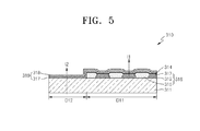
- FIG. 5 is an enlarged cross-sectional view of a portion 'V' of FIG. 4 .
- the image display device 3 includes a first display panel 310, a second display panel 320, and an image shift unit 330 disposed between the first display panel 210 and the second display panel 220.
- the first display panel 310 includes the first image display portion D11 that is disposed on a substrate 311 and displays the first image I1, the second image display portion D12 that is disposed outside the first image display portion D11 and displays the second image 12, and a sealing member 319 including a plurality of thin films that are stacked on the first image display portion D11 and the second image display portion D12.
- the substrate 311 is formed of a transparent material.
- the first image 11 is emitted from a first organic light-emitting portion 316 of the first display panel 310.
- the first organic light-emitting portion 316 includes an organic light-emitting layer 313 interposed between a first electrode 312 and a second electrode 314.
- first electrode 312 and the second electrode 314 function as an anode or a cathode by applying a voltage to the first electrode 312 and the second electrode 314.
- electrons and holes injected from the first electrode 312 and the second electrode 314 are combined with the organic light-emitting layer 313 to form excitons, and the organic light-emitting layer 313 emits light by the excitons to realize the first image I1.
- the image display device 3 may have high resolution, high image quality, low power consumption, and long lifetime.
- the first electrode 312 may function as a reflective electrode
- the second electrode 314 may function as a transparent electrode.
- the first electrode 312 may include a reflective layer formed of one selected from the group consisting of Ag, Mg, Al, Pt, Pd, Au, Ni, Nd, Ir, Cr and combinations thereof, and a transparent layer formed of ITO, IZO, ZnO or In 2 O 3 .
- the second electrode 314 may be formed of a transparent conductive material such as ITO, IZO, ZnO, or In 2 O 3 .
- the organic light-emitting layer 313 may be formed of a low molecular weight organic material or a high molecular weight organic material. When a low molecular weight organic film is included, the organic light-emitting layer 313 may have a single or multi-layer structure including at least one selected from the group consisting of a hole injection layer (HIL) (not shown), a hole transport layer (HTL) (not shown), an electron transport layer (ETL) (not shown), and an electron injection layer (EIL) (not shown).
- HIL hole injection layer
- HTL hole transport layer
- ETL electron transport layer
- EIL electron injection layer
- the organic light-emitting layer 313 may further include a HTL that is disposed in a direction from the organic light-emitting layer 313 towards an anode.
- the HTL may be formed of poly(ethylenedioxythiophene) (PEDOT), and the EML may be formed of polyphenylenevinylenes (PPVs) or polyfluorenes.
- the image display device 3 including the first organic light-emitting portion 316 may be classified into a passive matrix (PM) type and an active matrix (AM) type.
- PM passive matrix
- AM active matrix
- FIGS. 4 and 5 an example of an AM type image display is illustrated.
- the image display device 3 may include at least one thin film transistor (TFT) disposed below the first electrode 321 of each pixel.
- TFT thin film transistor
- a TFT electrically connected to the first electrode 321 is a driving TFT, and applies a signal of the first image It to each pixel.
- a pixel definition layer 315 defines each pixel of the AM type image display device 3. Each pixel includes a combination of red, green and blue light-emitting layers so as to realize various colors.
- the first image display portion D11 of the first display panel 310 includes the first organic light-emitting portion 316 emitting the first image I1.
- the second image display portion D12 of the first display panel 310 does not include a separate organic light-emitting portion.
- the second image display portion D12 of the first display panel 310 is maintained as a dead space, i.e., a non-emissive portion.
- the sealing member 319 including a plurality of thin films is stacked on the first image display portion D11 and the second image display portion D12 of the first display panel 310.
- the sealing member 319 is used in order to prevent external moisture and oxygen from penetrating into the organic light-emitting layer 313.
- a sealing substrate formed of transparent glass is used as the sealing member 319, a sealant (not shown) for sealing a space between the sealing substrate and the substrate 311 needs to be formed between the substrate 311 and the sealing substrate. In this case, due to the sealing substrate and the sealant formed on a dead space, i.e., a non-emissive portion, of the image display device 3, it may be difficult to display the second image 12.
- the image display device 3 includes the sealing member 319 that completely covers the first image display portion D11 and the second image display portion D12 of the substrate 311, instead of a sealing substrate including a separate sealant as a sealing member.
- the sealing member 319 is configured by stacking a single inorganic layer 317 and a single organic layer 318, but the present embodiment is not limited thereto. That is, the inorganic layer 317 and the organic layer 318 may be alternately stacked several times, or a plurality of inorganic layers or a plurality of organic layers may be stacked.
- the sealing member 319 is transparent, and is stacked on the substrate 311 without any sealant, the second image 12 emitted from the second display panel 320 may be displayed.
- the second display panel 320 is spaced apart from the first display panel 310, and is disposed inside the image display device 3.
- the second display panel 320 includes the second image emitting portion D22 disposed on a substrate 321 and displaying the second image 12, and a sealing member 329 including a plurality of thin films and disposed on the second image display portion D22.
- the second image 12 is emitted from a second organic light-emitting portion 326 of the second display panel 320.
- the second organic light-emitting portion 326 includes an organic light-emitting layer interposed between a first electrode and a second electrode, like the first organic light-emitting portion 316.
- the image shift unit 330 is disposed between the first display panel 310 and the second display panel 320.
- the image shift unit 330 shifts the second image 12 displayed on the second display panel 320 to the second image display portion D12 of the first display panel 310.
- the image shift unit 330 includes a first reflective surface 331 for reflecting the second image 12 emitted from the second organic light-emitting portion 326 of the second display panel 320, and a second reflective surface 332 that is disposed substantially parallel to the first reflective surface 331, and reflects the second image 12 reflected on the first reflective surface 331 to the second image display portion D12 of the first display panel 310, as in the image shift unit 130 of the image display device 1.
- the image display device 3 is an organic light-emitting display in which the image shift unit 330 is interposed between the first display panel 310 and the second display panel 320, but the present embodiment is not limited thereto. That is, the image shift unit 330 may be disposed on rear surfaces of the first display panel 310 and the second display panel 320, like in the image display device 2. In one embodiment, a display surface of the second display panel 320 on which the second image 12 is displayed faces away from the first display panel 310.
- the image shift unit 330 since the image shift unit 330 is disposed on a rear surface of the second display panel 320, the image shift unit 330 may shift the second image 12 emitted from the second display panel 320 to the second image display portion D12 of the first display panel 310 by reflecting the second image 12.
- the image display device 3 includes the sealing member 319 formed by stacking transparent thin films, instead of a sealing substrate that is completely adhered to the first image display portion D11 and the second image display portion D12 of the first display panel 310 by using a sealant, the second image 12 emitted from the second display panel 320 is displayed on the second image display portion D12 of the first display panel 310.
- the second image 12 is displayed on the second image display portion D12 of the first display panel 310, which is a dead space, i.e., as a non-emissive portion, thereby substantially removing the dead space.
- the image shift unit has been generally described as reflecting the generated second image towards the second image display portion of the first display panel, the invention is not limited to a reflecting arrangement, and only envisages that the image is transferred, guided or directed in some way towards the second image display portion.
Landscapes
- Engineering & Computer Science (AREA)
- Physics & Mathematics (AREA)
- Computer Hardware Design (AREA)
- General Physics & Mathematics (AREA)
- Theoretical Computer Science (AREA)
- Chemical & Material Sciences (AREA)
- Inorganic Chemistry (AREA)
- Microelectronics & Electronic Packaging (AREA)
- Electroluminescent Light Sources (AREA)
- Devices For Indicating Variable Information By Combining Individual Elements (AREA)
- Display Devices Of Pinball Game Machines (AREA)
Abstract
Description
- The described technology generally relates to an image display device and an organic-light emitting display including an image shift unit.
- An image display device such as an organic light-emitting display generally includes a dead space (i.e., a non-emissive portion) around an emissive portion on which an image is displayed. In order to minimize the size of the image display device and to maximize the size of a display portion, the dead space needs to be minimized.
- One inventive aspect is an image display device and an organic-light emitting display wherein a dead space (i.e., a non-emissive portion) is removed so that image quality is improved.
- Another aspect is an image display device which includes a first display panel including a first image display portion for displaying a first image, and a second image display portion that is disposed outside of the first image display portion and displays a second image; a second display panel that is spaced apart from the first display panel and displays the second image; and an image shift unit for shifting the second image displayed on the second display panel to the second image display portion of the first display panel.
- The first image display portion may include a first image light-emitting portion for emitting the first image, and the second display panel may include a second image emitting portion for emitting the second image.
- The second image display portion may be disposed on a non-emissive portion of the first display panel.
- The second image display portion may be transparent.
- The image shift unit may shift the second image displayed on the second display panel to the second image display portion according to a one to one correspondence.
- The image shift unit may be disposed between the first display panel and the second display panel.
- The image shift unit may include a first reflective surface for reflecting the second image emitted from the second display panel; and a second reflective surface that is disposed parallel to the first reflective surface, and reflects the second image reflected on the first reflective surface to the second image display portion.
- The first reflective surface and the second reflective surface may be respectively disposed on surfaces of a prism.
- The second display panel may be disposed between the first display panel and the image shift unit.
- The image shift unit may include a first reflective surface for reflecting the second image emitted from the second display panel; and a second reflective surface that is disposed to be symmetrical with the first reflective surface, and reflects the second image reflected on the first reflective surface to the second image display portion.
- The first reflective surface and the second reflective surface may be respectively disposed on a first reflective mirror and a second reflective mirror that are spaced apart from each other.
- The second image display portion may be disposed so as to directly contact an outside area of the first image display portion.
- The second image displayed on the second image display portion may be displayed together with an image displayed on the first image display portion, to form a single image.
- The first display panel may be a flat display panel.
- Another aspect is an organic light-emitting display including a first organic light-emitting display panel including: a first image display portion that is disposed on a substrate, includes a first organic light-emitting portion, and displays a first image emitted from the first organic light-emitting portion; a second image displaying portion that is disposed outside of the first image displaying portion and displays a second image; and a sealing member of a thin film that is stacked on the first image displaying portion and the second image displaying portion; a second organic light-emitting display panel that is spaced apart from the first display panel, and includes a second organic light-emitting portion for emitting the second image; and an image shit unit for shifting the second image emitted from the second organic light-emitting portion to the second image displaying portion of the first organic light-emitting display panel.
- The sealing member may be configured by alternately stacking an organic layer and an inorganic layer.
- The sealing member may be transparent.
- The first organic light-emitting display panel may include a first image driver for applying an image signal to the first organic light-emitting portion.
- The second organic light-emitting display panel may include a second image driver for applying an image signal to the second organic light-emitting portion.
- The image shift unit may shift the second image displayed on the second organic light-emitting display panel to the second image display portion according to one-to-one correspondence.
- The image shift unit may be disposed between the first organic light-emitting display panel and the second organic light-emitting display panel.
- The second organic light-emitting display panel may be disposed between the first organic light-emitting display panel and the image shift unit.
- Another aspect is an image display device comprising: a first display panel comprising i) a first image display portion configured to display a first image and ii) a light transmissive portion formed outside the first image display portion and configured to display a second image; a second display panel spaced apart from the first display panel and configured to generate the second image; and an image shift unit configured to shift the generated second image toward the light transmissive portion of the first display panel so that the shifted second image is projected through the light transmissive portion.
- In the above display device, the first image display portion comprises a first image light-emitting portion configured to emit the first image, and wherein the second display panel comprises a second image emitting portion configured to emit the second image.
- In the above display device, the light transmissive portion is formed on a non-emissive portion of the first display panel. In the above display, the first image display portion includes a self-emissive light emitting layer, and wherein the light transmissive portion does not include a self-emissive light emitting layer.
- In the above display device, the image shift unit is further configured to shift the generated second image toward the light transmissive portion according to a one to one image correspondence. In the above display, the image shift unit is formed between the first display panel and the second display panel. In the above display, the image shift unit comprises: a first reflective portion configured to first reflect the generated second image; and a second reflective portion formed substantially parallel to the first reflective portion, and configured to reflect the first reflected second image toward the light transmissive portion.
- In the above display device, the first and second reflective portions are respectively formed on opposing surfaces of a prism. In the above display, the second display panel is formed between the first display panel and the image shift unit. In the above display, the image shift unit comprises: a first reflective portion configured to first reflect the generated second image; and a second reflective portion formed to be substantially symmetrical with the first reflective portion, and configured to reflect the first reflected second image toward the light transmissive portion.
- In the above display device, the first and second reflective portions are respectively formed on a first reflective mirror and a second reflective mirror that are spaced apart from each other. In the above display, the light transmissive portion abuts the first image display portion. In the above display, the light transmissive portion is configured to transmit the second image substantially consecutively to the first image displayed on the first image display portion. In the above display, the second display panel is substantially vertically arranged with respect to the first display panel.
- Another aspect is an organic light-emitting display comprising: a first organic light-emitting display panel comprising: i) a first image display portion disposed on a substrate and configured to display a first image emitted from a first organic light-emitting portion, ii) a light transmissive portion substantially surrounding the first image display portion and configured to display a second image and iii) a sealing member formed on the first image display portion and the light transmissive portion; a second organic light-emitting display panel that is spaced apart from the first display panel, and comprises a second organic light-emitting portion configured to emit the second image; and an image transfer unit configured to transfer the emitted second image toward the light transmissive portion of the first organic light-emitting display panel so that the transferred second image is projected through the light transmissive portion.
- In the above display device, the sealing member comprises at least one organic layer and at least one inorganic layer which are alternately formed. In the above display, the sealing member is transparent. In the above display, the first image display portion of the first organic light-emitting display panel comprises a first image driver configured to apply an image signal to the first organic light-emitting portion, wherein the light transmissive portion of the first organic light-emitting display panel does not comprise an image driver, and wherein the second organic light-emitting display panel comprises a second image driver configured to apply an image signal to the second organic light-emitting portion.
- In the above display device, the second organic light-emitting display panel is substantially vertically arranged with respect to the first organic light-emitting display panel. In the above display, the image transfer unit is further configured to transfer the emitted second image toward the light transmissive portion according to one-to-one image correspondence. In the above display, the image transfer unit is formed between the first organic light-emitting display panel and the second organic light-emitting display panel. In the above display, the second organic light-emitting display panel is formed between the first organic light-emitting display panel and the image transfer unit.
- Another aspect is an organic light-emitting display comprising: a first organic light-emitting display panel comprising: i) a self-emissive region and ii) a non-self-emissive region; a second organic light-emitting display panel spaced apart from the first display panel and configured to emit an image; and an image transfer unit configured to transfer the emitted image toward the non-light emitting region of the first organic light-emitting display panel so that the transferred image is projected through the non-self-emissive region.
- Embodiments of the invention will now be described by way of example with reference to the accompanying drawings, in which:
-
FIG. 1 is a cross-sectional view of an image display device according to an embodiment. -
FIG. 2 is a plan view showing a first image and a second image displayed on a first display panel of the image display device ofFIG. 1 , according to an embodiment. -
FIG. 3 is a cross-sectional view of an image display device according to another embodiment. -
FIG. 4 is a cross-sectional view of an image display device according to another embodiment. -
FIG. 5 is an enlarged cross-sectional view of a portion 'V' ofFIG. 4 . - Referring to
FIG. 1 , the image display device 1 includes afirst display panel 110, asecond display panel 120, and an image shift unit (or image transfer unit) 130 disposed between thefirst display panel 110 and thesecond display panel 120. - The
first display panel 110 includes a first image display portion D11 displaying a first image I1, and a second image display portion D12 (or a light transmissive portion) disposed outside or substantially surrounding the first image display portion D11 and displaying asecond image 12. - In one embodiment, as shown in
FIG. 1 , the second image display portion D12 is disposed on four edge portions of the first image display portion D11. The second image display portion D12 may be disposed on at least one edge portion of the first image display portion D11. - Although not illustrated in
FIG. 1 in detail, the first image display portion D11 includes a first image emitting portion (not shown) for emitting the first image I1. For example, the first image emitting portion may include a plurality of light-emitting diodes including an organic self-emissive light-emitting material. Various colours may be realized by a combination of, for example, red, green and blue light-emitting diodes. Of course, the first image display portion D11 may further include a driver (not shown) for driving the first image emitting portion. - The second image display portion D12 may be disposed outside of the first image display portion D11 so as to directly contact the first image display portion D11. The second image display portion D12 does not include a separate image emitting portion, and thus does not include a driver for driving the light emitting portion.
- Thus, where an image is not displayed on the second image display portion D12 of the
first display panel 110, this portion acts as a dead space, that is, a non-emissive portion, of thefirst display panel 110. - Ideally, the second image display portion D12 of the
first display panel 110 displays thesecond image 12 emitted from thesecond display panel 120 without any change in brightness and colour. Thus, generally, the more transparent the second image display portion D12, the better the image display. Since the second image display portion D12 does not include a separate image emitting portion and driver, the second image display portion D12 may be transparent even when thesecond image 12 is not displayed on the second image display portion D12. In other words the second image display portion D12 comprises a transparent material. - As shown in
FIG. 1 , thesecond display panel 120 is spaced apart from thefirst display panel 110, and is disposed inside the image display device 1. - The
second display panel 120 includes a second image emitting portion D22 for generating thesecond image 12. - The second image emitting portion D22 may include a plurality of light-emitting diodes, like the first image emitting portion. A driver (not shown) for driving the second image emitting portion may be provided.
- The
image shift unit 130 is disposed between thefirst display panel 110 and thesecond display panel 120. Theimage shift unit 130 shifts or transfers thesecond image 12 provided by (displayed on) thesecond display panel 120 to the second image display portion D12 of thefirst display panel 110. - The
image shift unit 130 includes a first reflective surface 131 that reflects thesecond image 12 emitted from the second image emitting portion D22 of thesecond display panel 120, and a secondreflective surface 132 that is disposed substantially parallel to the first reflective surface 131, and reflects thesecond image 12 reflected on the first reflective surface 131 to the second image display portion D12 of thefirst display panel 110. - For example, the first reflective surface 131 and the second
reflective surface 132 may be respectively disposed on surfaces of a prism. According to the present embodiment, the first reflective surface 131 and the secondreflective surface 132 may be respectively disposed on surfaces of asingle prism 133 in the form of a parallelepiped. Alternatively, the first reflective surface 131 and the secondreflective surface 132 may be respectively disposed on surfaces of a reflective mirror (not shown) instead of a prism. - According to the present embodiment, the first reflective surface 131 and the second
reflective surface 132 are inclined at an inclination angle of about 45 degrees with respect to display surfaces of thefirst display panel 110 and thesecond display panel 120, but the present embodiment is not limited thereto. That is, by controlling the inclination angle of the first reflective surface 131 and the secondreflective surface 132, a distance between thefirst display panel 110 and thesecond display panel 120 may be controlled. -
FIG. 2 is a plan view showing the first image I1 and thesecond image 12 displayed on thefirst display panel 110 of the image display device 1 ofFIG. 1 , according to an embodiment. - In the image display device 1, the first image It emitted from the first image emitting portion of the
first display panel 110 is displayed on the first image display portion D11. Thesecond image 12 emitted from the second image emitting portion D22 of thesecond display panel 120, which is spaced apart from thefirst display panel 110, is shifted by theimage shift unit 130 disposed between thefirst display panel 110 and thesecond display panel 120, and then is displayed on the second image display portion D12 of thefirst display panel 110. Thus, thesecond image 12 is displayed on the second image display portion D12 of thefirst display panel 110, which is a dead space (i.e., a non-emissive portion), thereby removing the dead space. - The
second image 12 is displayed as a boundary image of the first image I1, and is contiguous with the first image I1, so that the first andsecond images - In some image display devices, since the resolution of an image file does not correspond to the resolution of the image display device, the entire image of the image file may not be displayed, and the image may appear to have been cropped. In this case, the part of the image that could not be displayed is displayed as the
second image 12 on thesecond display panel 120, and then is shifted to the second imagedisplay portion D 12 of thefirst display panel 110 by theimage shift unit 130 so as to be displayed as a boundary image that is displayed continguously with the first image I1. Thus, the entire image may be displayed without cropping, and may be displayed on a large-sized screen without any dead space. - Hereinafter, an image display device 2 according to another embodiment will be described with reference to
FIG. 3 . The image display device 2 will be described in terms of differences from the image display device 1 ofFIG. 1 , and like reference numerals may denote like elements in different drawings. - Referring to
FIG. 3 , the image display device 2 includes afirst display panel 210, asecond display panel 220, and animage shift unit 230 disposed at the rear of the first andsecond display panels - The
first display panel 210 includes the first image display portion D11 for displaying the first image I1, and the second image display portion D12 that is disposed outside of the first image display portion D11 and displays thesecond image 12. - The
second display panel 220 is spaced apart from thefirst display panel 210, and is disposed inside the image display device 1. Thesecond display panel 220 includes the second image emitting portion D22 for providing thesecond image 12. - As in
FIGS. 1 and 2 , the first image display portion D11 of thefirst display panel 210 includes a first image emitting portion (not shown) for emitting the first image I1, but the second image display portion D12 of thefirst display panel 210 does not include a separate image emitting portion. - The
image shift unit 230 is disposed at the rear of the first andsecond display panels FIG. 1 , thesecond display panel 120 is disposed so that a display surface of thesecond display panel 120, on which thesecond image 12 is displayed, faces thefirst display panel 110. On the other hand, inFIG. 3 , thesecond display panel 220 is disposed so that a display surface of thesecond display panel 220 on which thesecond image 12 is displayed faces away from thefirst display panel 210. - Thus, since the
image shift unit 230 is disposed at the rear of thesecond display panel 220, theimage shift unit 230 may shift thesecond image 12 emitted from thesecond display panel 220 to the second image display portion D12 of thefirst display panel 210 by reflecting thesecond image 12. - The
image shift unit 230 includes a firstreflective surface 231 for reflecting thesecond image 12 emitted from the second image emitting portion D22 of thesecond display panel 220, and a secondreflective surface 232 that is disposed to be substantially symmetric with the firstreflective surface 231, and reflects thesecond image 12 reflected on the firstreflective surface 231 to the second image display portion D12 of thefirst display panel 210. - The first
reflective surface 231 and the secondreflective surface 232 may be respectively disposed on surfaces of a substantially triangular prism, or alternatively, may be respectively disposed on surfaces of a reflective mirror (not shown) without a prism. - Hereinafter, an
image display device 3 according to another embodiment will be described with reference toFIGS. 4 and5 . Theimage display device 3 will be described in terms of differences from the image displays 1 and 2, and like reference numerals may denote like elements in different drawings. -
FIG. 4 is a cross-sectional view of animage display device 3 according to another embodiment.FIG. 5 is an enlarged cross-sectional view of a portion 'V' ofFIG. 4 . - Referring to
FIGS. 4 and5 , theimage display device 3 includes afirst display panel 310, asecond display panel 320, and animage shift unit 330 disposed between thefirst display panel 210 and thesecond display panel 220. - The
first display panel 310 includes the first image display portion D11 that is disposed on asubstrate 311 and displays the first image I1, the second image display portion D12 that is disposed outside the first image display portion D11 and displays thesecond image 12, and a sealingmember 319 including a plurality of thin films that are stacked on the first image display portion D11 and the second image display portion D12. - Since the
second image 12 emitted from thesecond display panel 320 is shifted to the second image display portion D12 of thefirst display panel 310 through thesubstrate 311, thesubstrate 311 is formed of a transparent material. - The
first image 11 is emitted from a first organic light-emittingportion 316 of thefirst display panel 310. - The first organic light-emitting
portion 316 includes an organic light-emittinglayer 313 interposed between afirst electrode 312 and asecond electrode 314. When thefirst electrode 312 and thesecond electrode 314 function as an anode or a cathode by applying a voltage to thefirst electrode 312 and thesecond electrode 314, electrons and holes injected from thefirst electrode 312 and thesecond electrode 314 are combined with the organic light-emittinglayer 313 to form excitons, and the organic light-emittinglayer 313 emits light by the excitons to realize the first image I1. Thus, theimage display device 3 may have high resolution, high image quality, low power consumption, and long lifetime. - Since the
image display device 3 is a top emission type that displays an image towards the sealingmember 319, thefirst electrode 312 may function as a reflective electrode, and thesecond electrode 314 may function as a transparent electrode. - The
first electrode 312 may include a reflective layer formed of one selected from the group consisting of Ag, Mg, Al, Pt, Pd, Au, Ni, Nd, Ir, Cr and combinations thereof, and a transparent layer formed of ITO, IZO, ZnO or In2O3. Thesecond electrode 314 may be formed of a transparent conductive material such as ITO, IZO, ZnO, or In2O3. - The organic light-emitting
layer 313 may be formed of a low molecular weight organic material or a high molecular weight organic material. When a low molecular weight organic film is included, the organic light-emittinglayer 313 may have a single or multi-layer structure including at least one selected from the group consisting of a hole injection layer (HIL) (not shown), a hole transport layer (HTL) (not shown), an electron transport layer (ETL) (not shown), and an electron injection layer (EIL) (not shown). Examples of available organic materials may include copper phthalocyanine (CuPc), N,N'-di(naphthalene-1-yl)-N,N'-diphenyl-benzidine (NPB), tris-8-hydroxyquinoline aluminum (Alq3), and the like. When a high-molecular weight organic layer is included, the organic light-emittinglayer 313 may further include a HTL that is disposed in a direction from the organic light-emittinglayer 313 towards an anode. In this case, the HTL may be formed of poly(ethylenedioxythiophene) (PEDOT), and the EML may be formed of polyphenylenevinylenes (PPVs) or polyfluorenes. - The
image display device 3 including the first organic light-emittingportion 316 may be classified into a passive matrix (PM) type and an active matrix (AM) type. InFIGS. 4 and5 , an example of an AM type image display is illustrated. Although not illustrated inFIGS. 4 and5 in detail, theimage display device 3 may include at least one thin film transistor (TFT) disposed below thefirst electrode 321 of each pixel. A TFT electrically connected to thefirst electrode 321 is a driving TFT, and applies a signal of the first image It to each pixel. - A
pixel definition layer 315 defines each pixel of the AM typeimage display device 3. Each pixel includes a combination of red, green and blue light-emitting layers so as to realize various colors. - The first image display portion D11 of the
first display panel 310 includes the first organic light-emittingportion 316 emitting the first image I1. On the other hand, the second image display portion D12 of thefirst display panel 310 does not include a separate organic light-emitting portion. Thus, where thesecond image 12 emitted from thesecond display panel 320 is not shifted to thefirst display panel 310, the second image display portion D12 of thefirst display panel 310 is maintained as a dead space, i.e., a non-emissive portion. - The sealing
member 319 including a plurality of thin films is stacked on the first image display portion D11 and the second image display portion D12 of thefirst display panel 310. - Since the organic light-emitting
layer 313 constituting the first organic light-emittingportion 316 of theimage display device 3 is generally vulnerable to moisture or oxygen, the sealingmember 319 is used in order to prevent external moisture and oxygen from penetrating into the organic light-emittinglayer 313. - If a sealing substrate formed of transparent glass is used as the sealing
member 319, a sealant (not shown) for sealing a space between the sealing substrate and thesubstrate 311 needs to be formed between thesubstrate 311 and the sealing substrate. In this case, due to the sealing substrate and the sealant formed on a dead space, i.e., a non-emissive portion, of theimage display device 3, it may be difficult to display thesecond image 12. - However, the
image display device 3 includes the sealingmember 319 that completely covers the first image display portion D11 and the second image display portion D12 of thesubstrate 311, instead of a sealing substrate including a separate sealant as a sealing member. - In
FIGS. 4 and5 , the sealingmember 319 is configured by stacking a singleinorganic layer 317 and a singleorganic layer 318, but the present embodiment is not limited thereto. That is, theinorganic layer 317 and theorganic layer 318 may be alternately stacked several times, or a plurality of inorganic layers or a plurality of organic layers may be stacked. - Since the sealing
member 319 is transparent, and is stacked on thesubstrate 311 without any sealant, thesecond image 12 emitted from thesecond display panel 320 may be displayed. - The
second display panel 320 is spaced apart from thefirst display panel 310, and is disposed inside theimage display device 3. - The
second display panel 320 includes the second image emitting portion D22 disposed on asubstrate 321 and displaying thesecond image 12, and a sealingmember 329 including a plurality of thin films and disposed on the second image display portion D22. - The
second image 12 is emitted from a second organic light-emittingportion 326 of thesecond display panel 320. - The second organic light-emitting
portion 326 includes an organic light-emitting layer interposed between a first electrode and a second electrode, like the first organic light-emittingportion 316. - The
image shift unit 330 is disposed between thefirst display panel 310 and thesecond display panel 320. Theimage shift unit 330 shifts thesecond image 12 displayed on thesecond display panel 320 to the second image display portion D12 of thefirst display panel 310. - The
image shift unit 330 includes a firstreflective surface 331 for reflecting thesecond image 12 emitted from the second organic light-emittingportion 326 of thesecond display panel 320, and a secondreflective surface 332 that is disposed substantially parallel to the firstreflective surface 331, and reflects thesecond image 12 reflected on the firstreflective surface 331 to the second image display portion D12 of thefirst display panel 310, as in theimage shift unit 130 of the image display device 1. - In
FIGS. 4 and5 , theimage display device 3 is an organic light-emitting display in which theimage shift unit 330 is interposed between thefirst display panel 310 and thesecond display panel 320, but the present embodiment is not limited thereto. That is, theimage shift unit 330 may be disposed on rear surfaces of thefirst display panel 310 and thesecond display panel 320, like in the image display device 2. In one embodiment, a display surface of thesecond display panel 320 on which thesecond image 12 is displayed faces away from thefirst display panel 310. In this embodiment, since theimage shift unit 330 is disposed on a rear surface of thesecond display panel 320, theimage shift unit 330 may shift thesecond image 12 emitted from thesecond display panel 320 to the second image display portion D12 of thefirst display panel 310 by reflecting thesecond image 12. - Since the
image display device 3 includes the sealingmember 319 formed by stacking transparent thin films, instead of a sealing substrate that is completely adhered to the first image display portion D11 and the second image display portion D12 of thefirst display panel 310 by using a sealant, thesecond image 12 emitted from thesecond display panel 320 is displayed on the second image display portion D12 of thefirst display panel 310. Thus, thesecond image 12 is displayed on the second image display portion D12 of thefirst display panel 310, which is a dead space, i.e., as a non-emissive portion, thereby substantially removing the dead space. - While the image shift unit has been generally described as reflecting the generated second image towards the second image display portion of the first display panel, the invention is not limited to a reflecting arrangement, and only envisages that the image is transferred, guided or directed in some way towards the second image display portion.
- While the disclosed embodiments have been particularly shown and described with reference to the accompanying drawings, it will be understood by those of ordinary skill in the art that various changes in form and details may be made therein without departing from the scope of the invention as defined by the claims.
Claims (15)
- An image display device comprising:a first display panel (110, 210, 310) comprising a first image display portion (D11) configured to display a first image and a light transmissive portion (D12) formed outside the first image display portion and configured to display a second image;a second display panel (120, 220, 320) spaced apart from the first display panel and configured to generate the second image; andan image shift unit (130, 230, 330) configured to shift the generated second image towards the light transmissive portion of the first display panel so that the shifted second image is projected through the light transmissive portion.
- The image display device of claim 1, wherein the first image display portion comprises a first image light-emitting portion configured to emit the first image, and wherein the second display panel comprises a second image emitting portion (D22) configured to emit the second image.
- The image display device of claim 1 or 2, wherein the light transmissive portion is formed on a non-emissive portion of the first display panel.
- The image display device of any one of the preceding claims, wherein the first image display portion includes a self-emissive light emitting layer, and wherein the light transmissive portion does not include a self-emissive light emitting layer.
- The image display device of any one of the preceding claims, wherein the image shift unit (130, 330) is formed between the first display panel and the second display panel.
- The image display device of claim 5, wherein the image shift unit comprises:a first reflective surface (131, 331) configured to reflect the generated second image; anda second reflective surface (132, 332) formed substantially parallel to the first reflective surface, and configured to further reflect the reflected second image toward the light transmissive portion.
- The image display device of claim 6, wherein the first and second reflective surfaces are respectively formed on opposing surfaces of a prism.
- The image display device of claim 6, wherein the first and second reflective surfaces comprises first and second mirrors.
- The image display device of any one of claims 1 to 4, wherein the second display panel is formed between the first display panel and the image shift unit (230).
- The image display device of claim 9, wherein the image shift unit comprises:a first reflective surface (231) configured to reflect the generated second image; anda second reflective surface (232) formed to be substantially symmetrical with the first reflective surface, and configured to further reflect the reflected second image toward the light transmissive portion.
- The image display device of claim 10, wherein the first and second reflective surfaces comprise first and second mirrors or reflective portions of a prism.
- The image display device of any one of the preceding claims, wherein the light transmissive portion abuts the first image display portion for displaying the first and second images contiguously.
- The image display device of any one of the preceding claims, wherein the first and second display panels are substantially parallel.
- An organic light-emitting display comprising an image display device according to any one of the preceding claims, wherein the first display panel comprises a first organic light-emitting display panel having a sealing member formed on the first image display portion and the light transmissive portion; and the second display panel comprises a second organic light-emitting display panel.
- The organic light-emitting display of claim 14, wherein the sealing member comprises at least one organic layer and at least one inorganic layer which are alternately formed.
Applications Claiming Priority (1)
| Application Number | Priority Date | Filing Date | Title |
|---|---|---|---|
| KR1020100057114A KR101694886B1 (en) | 2010-06-16 | 2010-06-16 | Image display apparatus and organic light emitting display apparatus comprising image shift unit |
Publications (2)
| Publication Number | Publication Date |
|---|---|
| EP2398006A2 true EP2398006A2 (en) | 2011-12-21 |
| EP2398006A3 EP2398006A3 (en) | 2013-01-23 |
Family
ID=44118069
Family Applications (1)
| Application Number | Title | Priority Date | Filing Date |
|---|---|---|---|
| EP11168253A Withdrawn EP2398006A3 (en) | 2010-06-16 | 2011-05-31 | Image Display Device and Organic Light-Emitting Display Including Image Shift Unit |
Country Status (4)
| Country | Link |
|---|---|
| US (2) | US8421708B2 (en) |
| EP (1) | EP2398006A3 (en) |
| KR (1) | KR101694886B1 (en) |
| CN (1) | CN102290429B (en) |
Families Citing this family (8)
| Publication number | Priority date | Publication date | Assignee | Title |
|---|---|---|---|---|
| US9244282B2 (en) * | 2011-10-12 | 2016-01-26 | Corning Incorporated | Curved bezel-concealing display device covers and bezel-free display devices |
| KR20140002470A (en) | 2012-06-29 | 2014-01-08 | 삼성디스플레이 주식회사 | Display device, manufacturing method of the same and manufacturing device of the same |
| US9439315B2 (en) | 2012-06-29 | 2016-09-06 | Samsung Display Co., Ltd. | Display device, and method and apparatus for manufacturing the same |
| KR101968310B1 (en) | 2012-11-28 | 2019-04-15 | 삼성디스플레이 주식회사 | Multi panel display apparatus |
| US20140267077A1 (en) * | 2013-03-15 | 2014-09-18 | Amazon Technologies, Inc. | User Device with a Primary Display and a Substantially Transparent Secondary Display |
| KR102380158B1 (en) | 2015-04-24 | 2022-03-29 | 삼성디스플레이 주식회사 | Display device and manufacturing method thereof |
| US9945539B1 (en) * | 2016-10-19 | 2018-04-17 | Lu Su | Backlit display assembly |
| US10658441B2 (en) * | 2017-08-28 | 2020-05-19 | Apple Inc. | Organic light-emitting diode displays with reflectors |
Citations (5)
| Publication number | Priority date | Publication date | Assignee | Title |
|---|---|---|---|---|
| WO2005062608A2 (en) * | 2003-12-18 | 2005-07-07 | Koninklijke Philips Electronics N.V. | Supplementary visual display system |
| US20050200273A1 (en) * | 2004-03-03 | 2005-09-15 | Seiko Epson Corporation | Light-emitting device, method of manufacturing light-emitting device, and electronic apparatus |
| WO2007026284A1 (en) * | 2005-08-31 | 2007-03-08 | Koninklijke Philips Electronics, N.V. | Ambient lighting through a hidden frame |
| US20070164975A1 (en) * | 2004-03-08 | 2007-07-19 | Koninklijke Philips Electronics, N.V. | Display device |
| US20080246692A1 (en) * | 2007-04-05 | 2008-10-09 | Samsung Electronics Co., Ltd. | Foldable multi-display apparatus |
Family Cites Families (10)
| Publication number | Priority date | Publication date | Assignee | Title |
|---|---|---|---|---|
| KR100211900B1 (en) | 1996-06-15 | 1999-08-02 | 구자홍 | The image display apparatus |
| KR20040005031A (en) | 2002-07-08 | 2004-01-16 | (주)드리맥스 | Optical system using single display device for head mounted display |
| JP2008505350A (en) | 2004-06-30 | 2008-02-21 | コーニンクレッカ フィリップス エレクトロニクス エヌ ヴィ | An active frame system for ambient light using a video display as a signal source. |
| WO2008065614A1 (en) * | 2006-11-30 | 2008-06-05 | Koninklijke Philips Electronics N.V. | A rim system for a display |
| RU2444151C2 (en) | 2007-01-03 | 2012-02-27 | Конинклейке Филипс Электроникс Н.В. | Display layout ambilight |
| ATE525855T1 (en) * | 2007-01-03 | 2011-10-15 | Koninkl Philips Electronics Nv | DISPLAY DEVICE WITH AMBIENT LIGHT |
| KR20080078263A (en) | 2007-02-22 | 2008-08-27 | 엘지디스플레이 주식회사 | Display device and image display system |
| KR101321373B1 (en) | 2007-03-16 | 2013-10-28 | 삼성전자주식회사 | Multi-display apparatus |
| JP2009037812A (en) * | 2007-07-31 | 2009-02-19 | Sumitomo Chemical Co Ltd | Organic EL device and manufacturing method thereof |
| US8638483B2 (en) | 2008-09-17 | 2014-01-28 | Konica Minolta Holdings, Inc. | Image display device and head-mounted display |
-
2010
- 2010-06-16 KR KR1020100057114A patent/KR101694886B1/en not_active Expired - Fee Related
-
2011
- 2011-03-08 US US13/043,379 patent/US8421708B2/en not_active Expired - Fee Related
- 2011-04-26 CN CN201110112485.XA patent/CN102290429B/en not_active Expired - Fee Related
- 2011-05-31 EP EP11168253A patent/EP2398006A3/en not_active Withdrawn
-
2013
- 2013-03-14 US US13/829,135 patent/US9147359B2/en not_active Expired - Fee Related
Patent Citations (5)
| Publication number | Priority date | Publication date | Assignee | Title |
|---|---|---|---|---|
| WO2005062608A2 (en) * | 2003-12-18 | 2005-07-07 | Koninklijke Philips Electronics N.V. | Supplementary visual display system |
| US20050200273A1 (en) * | 2004-03-03 | 2005-09-15 | Seiko Epson Corporation | Light-emitting device, method of manufacturing light-emitting device, and electronic apparatus |
| US20070164975A1 (en) * | 2004-03-08 | 2007-07-19 | Koninklijke Philips Electronics, N.V. | Display device |
| WO2007026284A1 (en) * | 2005-08-31 | 2007-03-08 | Koninklijke Philips Electronics, N.V. | Ambient lighting through a hidden frame |
| US20080246692A1 (en) * | 2007-04-05 | 2008-10-09 | Samsung Electronics Co., Ltd. | Foldable multi-display apparatus |
Also Published As
| Publication number | Publication date |
|---|---|
| CN102290429B (en) | 2016-04-06 |
| CN102290429A (en) | 2011-12-21 |
| US20130241809A1 (en) | 2013-09-19 |
| EP2398006A3 (en) | 2013-01-23 |
| KR20110137089A (en) | 2011-12-22 |
| US20110310128A1 (en) | 2011-12-22 |
| US8421708B2 (en) | 2013-04-16 |
| KR101694886B1 (en) | 2017-01-24 |
| US9147359B2 (en) | 2015-09-29 |
Similar Documents
| Publication | Publication Date | Title |
|---|---|---|
| US9147359B2 (en) | Image display and organic light-emitting display including image shift unit | |
| US8227796B2 (en) | Display device | |
| US9293515B2 (en) | Organic light-emitting display device and method of manufacturing the same | |
| US8174179B2 (en) | Organic light emitting display apparatus | |
| US8237354B2 (en) | Organic light emitting diode display | |
| US9391121B2 (en) | Organic light-emitting diode (OLED) display | |
| US7629740B2 (en) | Display device with stacked layer body | |
| US8550667B2 (en) | Optical film and organic light emitting display apparatus including the same | |
| US8212242B2 (en) | Organic light emitting diode display having a corner-cube pattern cover layer | |
| CN103681746B (en) | Organic light-emitting display device and its manufacturing method | |
| US9343510B2 (en) | Organic light emitting display device | |
| US20100052519A1 (en) | Organic light emitting diode display | |
| KR20160069627A (en) | Organic light emitting display device and manufacturing method thereof | |
| US20100033078A1 (en) | Organic light emitting display device | |
| JP2013016466A (en) | Organic light emitting display device | |
| KR20160000096A (en) | Display device | |
| JP2012094513A (en) | Organic light-emitting display device | |
| US8193703B2 (en) | Organic light emitting diode display that directs reflected light to improve visibility | |
| JP2011129919A (en) | Blue light-emitting device and organic light emitting display including the same | |
| US8847210B2 (en) | Organic light emitting diode display | |
| KR20090128237A (en) | Organic light emitting display device | |
| US20240260410A1 (en) | Organic light-emitting diode display device and method of manufacturing the same | |
| US8223095B2 (en) | Organic light-emitting display device having a pixel unit for testing pixels of the display device | |
| KR100565742B1 (en) | Organic light emitting diode | |
| JP2006178335A (en) | Liquid crystal display device and method for manufacturing liquid crystal display device |
Legal Events
| Date | Code | Title | Description |
|---|---|---|---|
| AK | Designated contracting states |
Kind code of ref document: A2 Designated state(s): AL AT BE BG CH CY CZ DE DK EE ES FI FR GB GR HR HU IE IS IT LI LT LU LV MC MK MT NL NO PL PT RO RS SE SI SK SM TR |
|
| AX | Request for extension of the european patent |
Extension state: BA ME |
|
| PUAI | Public reference made under article 153(3) epc to a published international application that has entered the european phase |
Free format text: ORIGINAL CODE: 0009012 |
|
| RAP1 | Party data changed (applicant data changed or rights of an application transferred) |
Owner name: SAMSUNG DISPLAY CO., LTD. |
|
| PUAL | Search report despatched |
Free format text: ORIGINAL CODE: 0009013 |
|
| AK | Designated contracting states |
Kind code of ref document: A3 Designated state(s): AL AT BE BG CH CY CZ DE DK EE ES FI FR GB GR HR HU IE IS IT LI LT LU LV MC MK MT NL NO PL PT RO RS SE SI SK SM TR |
|
| AX | Request for extension of the european patent |
Extension state: BA ME |
|
| RIC1 | Information provided on ipc code assigned before grant |
Ipc: H01L 25/00 20060101ALI20121219BHEP Ipc: G02B 6/00 20060101ALI20121219BHEP Ipc: H04N 5/64 20060101ALI20121219BHEP Ipc: G09F 9/00 20060101AFI20121219BHEP |
|
| 17P | Request for examination filed |
Effective date: 20130723 |
|
| RBV | Designated contracting states (corrected) |
Designated state(s): AL AT BE BG CH CY CZ DE DK EE ES FI FR GB GR HR HU IE IS IT LI LT LU LV MC MK MT NL NO PL PT RO RS SE SI SK SM TR |
|
| 17Q | First examination report despatched |
Effective date: 20140923 |
|
| RAP1 | Party data changed (applicant data changed or rights of an application transferred) |
Owner name: SAMSUNG DISPLAY CO., LTD. |
|
| APBK | Appeal reference recorded |
Free format text: ORIGINAL CODE: EPIDOSNREFNE |
|
| APBN | Date of receipt of notice of appeal recorded |
Free format text: ORIGINAL CODE: EPIDOSNNOA2E |
|
| APBR | Date of receipt of statement of grounds of appeal recorded |
Free format text: ORIGINAL CODE: EPIDOSNNOA3E |
|
| APAF | Appeal reference modified |
Free format text: ORIGINAL CODE: EPIDOSCREFNE |
|
| STAA | Information on the status of an ep patent application or granted ep patent |
Free format text: STATUS: EXAMINATION IS IN PROGRESS |
|
| APBT | Appeal procedure closed |
Free format text: ORIGINAL CODE: EPIDOSNNOA9E |
|
| STAA | Information on the status of an ep patent application or granted ep patent |
Free format text: STATUS: THE APPLICATION IS DEEMED TO BE WITHDRAWN |
|
| 18D | Application deemed to be withdrawn |
Effective date: 20181201 |