EP2395608A1 - Connector with a laterally moving contact - Google Patents
Connector with a laterally moving contact Download PDFInfo
- Publication number
- EP2395608A1 EP2395608A1 EP11169816A EP11169816A EP2395608A1 EP 2395608 A1 EP2395608 A1 EP 2395608A1 EP 11169816 A EP11169816 A EP 11169816A EP 11169816 A EP11169816 A EP 11169816A EP 2395608 A1 EP2395608 A1 EP 2395608A1
- Authority
- EP
- European Patent Office
- Prior art keywords
- contact
- connector
- mating
- contacts
- interface
- Prior art date
- Legal status (The legal status is an assumption and is not a legal conclusion. Google has not performed a legal analysis and makes no representation as to the accuracy of the status listed.)
- Withdrawn
Links
- 230000013011 mating Effects 0.000 claims abstract description 177
- 239000000758 substrate Substances 0.000 description 22
- 239000004020 conductor Substances 0.000 description 13
- 229910052751 metal Inorganic materials 0.000 description 12
- 239000002184 metal Substances 0.000 description 12
- 229910001092 metal group alloy Inorganic materials 0.000 description 12
- 150000002739 metals Chemical class 0.000 description 11
- 238000011109 contamination Methods 0.000 description 10
- 230000008878 coupling Effects 0.000 description 8
- 238000010168 coupling process Methods 0.000 description 8
- 238000005859 coupling reaction Methods 0.000 description 8
- 230000006835 compression Effects 0.000 description 6
- 238000007906 compression Methods 0.000 description 6
- 230000001154 acute effect Effects 0.000 description 5
- 239000011248 coating agent Substances 0.000 description 5
- 238000000576 coating method Methods 0.000 description 5
- 239000000463 material Substances 0.000 description 4
- 229920000642 polymer Polymers 0.000 description 2
- 229920001940 conductive polymer Polymers 0.000 description 1
- 238000006073 displacement reaction Methods 0.000 description 1
- 230000001788 irregular Effects 0.000 description 1
- 239000000203 mixture Substances 0.000 description 1
- 230000037361 pathway Effects 0.000 description 1
- 239000012858 resilient material Substances 0.000 description 1
Images








Classifications
-
- H—ELECTRICITY
- H01—ELECTRIC ELEMENTS
- H01R—ELECTRICALLY-CONDUCTIVE CONNECTIONS; STRUCTURAL ASSOCIATIONS OF A PLURALITY OF MUTUALLY-INSULATED ELECTRICAL CONNECTING ELEMENTS; COUPLING DEVICES; CURRENT COLLECTORS
- H01R12/00—Structural associations of a plurality of mutually-insulated electrical connecting elements, specially adapted for printed circuits, e.g. printed circuit boards [PCB], flat or ribbon cables, or like generally planar structures, e.g. terminal strips, terminal blocks; Coupling devices specially adapted for printed circuits, flat or ribbon cables, or like generally planar structures; Terminals specially adapted for contact with, or insertion into, printed circuits, flat or ribbon cables, or like generally planar structures
- H01R12/70—Coupling devices
- H01R12/91—Coupling devices allowing relative movement between coupling parts, e.g. floating or self aligning
-
- H—ELECTRICITY
- H01—ELECTRIC ELEMENTS
- H01R—ELECTRICALLY-CONDUCTIVE CONNECTIONS; STRUCTURAL ASSOCIATIONS OF A PLURALITY OF MUTUALLY-INSULATED ELECTRICAL CONNECTING ELEMENTS; COUPLING DEVICES; CURRENT COLLECTORS
- H01R13/00—Details of coupling devices of the kinds covered by groups H01R12/70 or H01R24/00 - H01R33/00
- H01R13/02—Contact members
- H01R13/22—Contacts for co-operating by abutting
- H01R13/24—Contacts for co-operating by abutting resilient; resiliently-mounted
- H01R13/2407—Contacts for co-operating by abutting resilient; resiliently-mounted characterized by the resilient means
-
- H—ELECTRICITY
- H01—ELECTRIC ELEMENTS
- H01R—ELECTRICALLY-CONDUCTIVE CONNECTIONS; STRUCTURAL ASSOCIATIONS OF A PLURALITY OF MUTUALLY-INSULATED ELECTRICAL CONNECTING ELEMENTS; COUPLING DEVICES; CURRENT COLLECTORS
- H01R13/00—Details of coupling devices of the kinds covered by groups H01R12/70 or H01R24/00 - H01R33/00
- H01R13/62—Means for facilitating engagement or disengagement of coupling parts or for holding them in engagement
- H01R13/629—Additional means for facilitating engagement or disengagement of coupling parts, e.g. aligning or guiding means, levers, gas pressure electrical locking indicators, manufacturing tolerances
- H01R13/631—Additional means for facilitating engagement or disengagement of coupling parts, e.g. aligning or guiding means, levers, gas pressure electrical locking indicators, manufacturing tolerances for engagement only
- H01R13/6315—Additional means for facilitating engagement or disengagement of coupling parts, e.g. aligning or guiding means, levers, gas pressure electrical locking indicators, manufacturing tolerances for engagement only allowing relative movement between coupling parts, e.g. floating connection
-
- H—ELECTRICITY
- H01—ELECTRIC ELEMENTS
- H01R—ELECTRICALLY-CONDUCTIVE CONNECTIONS; STRUCTURAL ASSOCIATIONS OF A PLURALITY OF MUTUALLY-INSULATED ELECTRICAL CONNECTING ELEMENTS; COUPLING DEVICES; CURRENT COLLECTORS
- H01R13/00—Details of coupling devices of the kinds covered by groups H01R12/70 or H01R24/00 - H01R33/00
- H01R13/02—Contact members
- H01R13/22—Contacts for co-operating by abutting
- H01R13/24—Contacts for co-operating by abutting resilient; resiliently-mounted
- H01R13/2407—Contacts for co-operating by abutting resilient; resiliently-mounted characterized by the resilient means
- H01R13/2421—Contacts for co-operating by abutting resilient; resiliently-mounted characterized by the resilient means using coil springs
Definitions
- the invention relates to an electrical connector having a contact that engages a contact pad of a mating connector.
- Known electrical connectors include contacts disposed within or coupled with a housing. The housings mate with one another to electrically couple the contacts. Once the contacts are joined with one another, the connectors communicate data signals and/or power between each other via the coupled contacts.
- Some known connectors include contacts that mate with contact pads of another connector.
- a connector system may include a first connector that includes several contacts while a second connector includes several substantially flat contact pads.
- the second connector may be a printed circuit board that includes contact pads disposed on one side of the board. The contacts engage the contact pads to electrically couple the contacts with the contact pads.
- the contact pads may include or be formed from metals or metal alloys that may develop an insulating layer of surface contamination when exposed to the environment over time. This layer may be present on the surface of the contact pads that mate with the first connector. The layer may negatively impact the coupling between the connector and the contact pads. For example, the layer may have a greater resistivity than the contact pad and increase the resistance of the coupling between the contacts and the contact pads.
- the layer of surface contamination may be locally removed from the contact pad by laterally moving the contact across the surface of the contact pad. The lateral movement of the contact may scrape off or otherwise remove the layer of surface contamination from a portion of the contact pad. The contact engages the contact pad where the layer has been removed for an improved electrical coupling between the contact and the contact pad.
- the connector in which the contact is disposed in order to laterally move the contact across the contact pad and remove the layer of surface contamination, the connector in which the contact is disposed must be laterally moved with respect to the connector that includes the contact pad. In some applications, there is insufficient room to laterally move the connectors relative to each other. Additionally, lateral movement of the connectors relative to each other may result in misalignment of the contacts relative to the contact pads. Such misalignment may prevent some of the contacts from mating with the contact pads.
- a connector comprises a housing and a contact coupled with the housing.
- the contact has a mating end and an interface end.
- An angled interface is disposed within the housing and arranged for sliding engagement with the interface end of the contact.
- Figure 1 is an elevational view of a decoupled connector system in accordance with one embodiment of the present disclosure.
- Figure 2 is an elevational view of a coupled or mated connector system in accordance with one embodiment of the present disclosure.
- Figure 3 is an illustration of a front end of a connector shown in Figure 1 in accordance with one embodiment of the present disclosure.
- Figure 4 is a schematic illustration of a contact of the connector shown in Figure 1 in an initial position also shown in Figure 1 in accordance with one embodiment of the present disclosure.
- Figure 5 is a schematic illustration of the contact shown in Figure 1 in a mated position shown in Figure 2 in accordance with one embodiment of the present disclosure.
- Figure 6 is a schematic illustration of a contact disposed within the connector shown in Figure 1 in an initial position in accordance with an alternative embodiment of the present disclosure.
- Figure 7 is a schematic illustration of the contact shown in Figure 6 disposed within the connector shown in Figure 1 in a subsequent mated position in accordance with one embodiment of the present disclosure.
- Figure 8 is a schematic illustration of a contact in a connector in an initial position in accordance with an alternative embodiment of the present disclosure.
- Figure 9 is a schematic illustration of the contact shown in Figure 8 disposed within the connector shown in Figure 8 in a mated position.
- Figure 10 is a schematic illustration of a contact disposed within a connector in an initial position in accordance with an alternative embodiment of the present disclosure.
- Figure 11 is a schematic illustration of a contact disposed within a connector in an initial position in accordance with an alternative embodiment of the present disclosure.
- Figure 12 is a schematic illustration of a contact in an initial position within a connector in accordance with an alternative embodiment of the present disclosure.
- Figure 13 is a schematic illustration of the contact (shown in Figure 12 ) of the connector (shown in Figure 12 ) in a mated position in accordance with one embodiment of the present disclosure.
- Figure 14 is a schematic illustration of a contact disposed within a connector in an initial position in accordance with an alternative embodiment of the present disclosure.
- Figure 15 is a perspective view of a connector system in accordance with another embodiment.
- Figure 16 is a cross-sectional view of the connector system shown in Figure 15 in an unmated state along line A-A in Figure 15 .
- Figure 17 is a detail view of a portion of the connector system shown in Figure 16 .
- Figure 18 is a cross-sectional view of the connector system shown in Figure 15 in a partially mated state along line A-A in Figure 15 .
- Figure 19 is a detail view of a portion of the connector system shown in Figure 18 .
- Figure 20 is a cross-sectional view of the connector system shown in Figure 15 in a mated state along line A-A in Figure 15 .
- Figure 21 is a detail view of a portion of the connector system shown in Figure 20 .
- Figure 22 is a perspective view of a connector system in accordance with another embodiment.
- Figure 23 is a cross-sectional view of the connector system shown in Figure 22 in an unmated state along line B-B in Figure 22 .
- Figure 24 is a detail view of a portion of the connector system shown in Figure 23 .
- Figure 25 is a cross-sectional view of the connector system shown in Figure 22 in a partially mated state along line B-B in Figure 22 .
- Figure 26 is a detail view of a portion of the connector system shown in Figure 25 .
- Figure 27 is a cross-sectional view of the connector system shown in Figure 22 in a mated state along line B-B in Figure 22 .
- Figure 28 is a detail view of a portion of the connector system shown in Figure 27 .
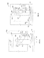
- Figure 1 is an elevational view of a decoupled connector system 100 in accordance with one embodiment of the present disclosure.
- Figure 2 is an elevational view of a coupled or mated connector system 100 in accordance with one embodiment of the present disclosure.
- the system 100 includes two connectors 102, 104 that mate with one another to communicate data signals and/or electric power between the connectors 102, 104.
- the connector 104 may be referred to herein as a mating connector.
- the first connector 102 includes a housing 112 that extends from a front end 114 to a back end 116.
- Several contacts 106 are disposed within the housing 112 and protrude from the front end 114.
- the contacts 106 may be recessed within the housing 112 such that the contacts 106 do not protrude from the front end 114.
- the number of contacts 106 shown in Figures 1 and 2 is provided merely as an example.
- the contacts 106 engage corresponding conductive elements 108 of the second connector 104.
- the contact 106 and the conductive element 108 include, or are formed from, conductive materials, such as metals or metal alloys.
- the contacts 106 of the first connector 102 are elongated contacts.
- the contacts 106 may be non-elongated contacts.
- the contacts 106 may not be elongated in a mating direction 110 that the first connector 102 and/or second connector 104 are moved relative to each other.
- the second, or mating, connector 104 may be a circuit board, such as a printed circuit board (PCB), with the conductive elements 108 being contacts that mate with the contacts 106.
- the conductive elements 108 may be substantially flat contact pads disposed on one side of the circuit board. The number of conductive elements 108 is shown merely as an example.
- the second connector 104 may be a connector other than a circuit board.
- the connectors 102, 104 mate with one another by moving the first connector 102 toward the second connector 104 in the mating direction 110 or by moving the second connector 104 in a direction that is opposite of the mating direction 110 until the contacts 106 of the first connector 102 engage the conductive elements 108 of the second connector 104.
- at least one of the connectors 102, 104 is moved toward the other of the connectors 102, 104.
- the mating direction 110 is oriented approximately parallel to a longitudinal axis 304 of the contact 106.
- each of the contacts 106 Prior to mating the connectors 102, 104, each of the contacts 106 is located at an initial position 118 at the front end 114 of the housing 112.
- the spacing between the initial positions 118 of adjacent contacts 106 may be uniform or non-uniform across the front end 114.
- the initial position 118 of each contact 106 may correspond to the location of the longitudinal axis 304 of the contact 106 along the front end 114.
- the conductive elements 108 of the second connector 104 may have center lines or axes 120 that extend through the center of the conductive elements 108. As shown in Figure 1 , the longitudinal axes 304 of the contacts 106 are laterally spaced apart from the center axes 120 of the conductive elements 108.
- the longitudinal axis 304 of a contact 106 and the center axis 120 of a conductive element 108 that mates with the contact 106 may be spaced apart by a lateral gap 122 along a direction that is transverse or perpendicular to the longitudinal axis 304.
- the contacts 106 are caused to move laterally across the conductive elements 108 as will be explained in more detail hereinbelow.
- the contacts 106 wipe across the upper surfaces of the conductive elements 108 in wiping directions 200A, 200B that are oriented perpendicular to the mating direction 110.
- Some contacts 106 may move in the wiping direction 200A while other contacts 106 move in the wiping direction 200B toward the center axes 120 of the conductive elements 108.
- Different subsets of the contacts 106 in the array may move in different wiping directions 200A, 200B.
- the wiping direction 200A of one subset of contacts 106 may be oriented opposite of the wiping direction 200B of another subset of contacts 106.
- all of the contacts 106 may move in a common wiping direction 200A or 200B.
- the contacts 106 laterally move in the wiping directions 200A, 200B from the initial positions 118 to mated positions 202 (shown in Figure 2 ).
- the contacts 106 are laterally displaced by a lateral distance 204 when the connectors 102, 104 mate.
- the lateral distance 204 is approximately the same as the lateral gap 122 (shown in Figure 1 ) between the initial positions 118 of the contacts 106 and the center axes 120 of the conductive elements 108 such that the longitudinal axes 304 of the contacts 106 are aligned with the center axes 120 of the conductive elements 108.
- the contacts 106 may move in the wiping direction 200 relative to the connectors 102, 104.
- the connectors 102, 104 may move relative to each other such that the connectors 102, 104 move toward one another along the mating direction 110 while the contacts 106 simultaneously or concurrently move in the lateral wiping directions 200A, 200B.
- the contacts 106 may move in the wiping directions 200A, 200B independent of the movement of the connector 102 to prevent misalignment of the contacts 106 with the conductive elements 108. For example, if the contacts 106 were able to laterally move across the conductive elements 108 only if the connector 102 also moved in the wiping direction 200A or 200B, then the contacts 106 may become misaligned with the conductive elements 108.
- the independent lateral movement of the contacts 106 permits an operator to align the connectors 102, 104 with one another along the mating direction 110 while still achieving a wiping motion of the contacts 106 across the conductive elements 108 in the wiping directions 200A, 200B.
- the wiping movement of the contacts 106 across the conductive elements 108 may improve an electrical coupling between the contacts 106 and conductive elements 108.
- the wiping movement of the contacts 106 across the conductive elements 108 may remove one or more layers of surface contamination on the conductive elements 108. Removal of the surface contamination may reduce the resistivity of the coupling between the contacts 106 and conductive elements 108.
- the contacts 106 laterally move in the wiping directions 200A, 200B relative to both the housing 112 of the connector 102 and the connector 104.
- the contacts 106 move within the housing 112 without the housing 112 laterally moving with respect to the connector 104.
- the contacts 106 may return to the initial positions 118 when the connectors 102, 104 decouple from one another.
- the connector 102 may be retreated away from the connector 104 in a decoupling direction 206 (shown in Figure 2 ) to separate the contacts 106 and conductive elements 108 from one another and break the electrical coupling between the contacts 106 and conductive elements 108.
- the contacts 106 return to the initial positions 118 as shown in Figure 1 .
- the contacts 106 may laterally move within and relative to the housing 112 back to the initial positions 118.
- FIG. 3 is an illustration of the front end 114 of the connector 102 in accordance with one embodiment of the present disclosure.
- Channels 310 may be arranged in an array across the front end 114.
- Each of the channels 310 is bounded by opposing end walls 312, 314 and opposing side walls 704, 706.
- the channels 310 include contacts 106 that protrude from the front end 114.
- the contacts 106 move in the wiping directions 200A, 200B within the channels 310 during mating of the connector 102 with the connector 104. In the illustrated embodiment, different subsets of the contacts 106 move in different wiping directions 200A, 200B.
- some contacts 106 may move in a wiping direction 200A from the wall 312 toward the wall 314 while other contacts 106 move in a wiping direction 200B from the wall 314 toward the wall 312.
- the channels 310 may extend inward from the front end 114 to define openings 700 along the front end 114.
- the openings 700 are elongated in directions parallel to the wiping directions 200A, 200B.
- the openings 700 have a width dimension 702 in a direction that is angled with respect to the corresponding wiping direction 200A or 200B.
- the width dimension 702 may extend in a direction that is perpendicular to the wiping direction 200A or 200B of the contact 106 in the channel 310.
- the width dimension 702 may be sufficiently large to permit movement of the contacts 106 in the wiping direction 200A or 200B, but small enough to constrain movement of the contacts 106 to the wiping direction 200A or 200B.
- the width dimension 702 may be slightly larger than a width dimension 708 of the contacts 106 to permit movement of the contacts 106 in the wiping directions 200A, 200B yet prevent significant movement of the contacts 106 in directions that are angled with respect to the wiping directions 200A, 200B.
- Figure 4 is a schematic illustration of one of the contacts 106 of the connector 102 in the initial position 118 (shown in Figure 1 ) in accordance with one embodiment of the present disclosure.
- Figure 5 is a schematic illustration of the contact 106 in the mated position 202 (shown in Figure 2 ) with respect to the conductive element 108 in accordance with one embodiment of the present disclosure.
- the contact 106 is disposed within a channel 310 of the housing 112 (shown in Figure 1 ).
- the channel 310 may be an interior section of the housing 112 that is bounded by opposing end walls 312, 314 and an interconnecting wall 316.
- the channel 310 is located inside the housing 112 with the interconnecting wall 316 separated from the back end 116 of the housing 112.
- the interconnecting wall 316 and the back end 116 may be the same component or portion of the housing 112.
- the front end 114 of the housing 112 opposes the interconnecting wall 316.
- the contact 106 may be an elongated contact that extends from an interface end 302 to a mating end 300 along the longitudinal axis 304.
- the contact 106 may be a non-elongated contact.
- the contact 106 may not be longer between the interface end 302 and the mating end 300 than in another direction.
- the mating end 300 is shown as a rounded tip, alternatively the mating end 300 may have a different shape.
- the illustrated interface end 302 includes sides 306, 308 that are angled with respect to one another.
- the sides 306, 308 may be approximately planar surfaces that are obliquely or perpendicularly oriented with respect to each other.
- the sides 306, 308 also are angled with respect to the longitudinal axis 304. In the illustrated embodiment, the sides 306, 308 are oriented at approximately 45 degrees with respect to the longitudinal axis 304. In another embodiment, one or more of the sides 306, 308 may be oriented at a different angle with respect to the longitudinal axis 304. Alternatively, the interface end 302 includes only the side 306. In another embodiment, the interface end 302 may be rounded in a manner similar to the mating end 300.
- the channel 310 includes an angled interface 318 that is angled with respect to the longitudinal axis 304 of the contact 106.
- the angled interface 318 may include a sliding surface 320 that is obliquely oriented with respect to the longitudinal axis 304.
- the sliding surface 320 may be oriented at an angle 328 with respect to the longitudinal axis 304.
- the angle 328 is an acute angle of approximately 45 degrees.
- the angle 328 may be a different angle, such as 30 degrees.
- the sliding surface 320 may include or be formed from a conductive material, such as one or more metals or metal alloys.
- the angled interface 318 and/or sliding surface 320 may be electrically coupled with a source or recipient (not shown) of the data and/or power that is electrically communicated between the connectors 102, 104.
- the sliding surface 320 may be a contact pad similar to the conductive element 108 that receives data signals communicated from the connector 104 to the connector 102 via the contacts 106 and conductive elements 108.
- the angled interface 318 is slidably coupled with the interface end 302 of the contact 106.
- the angled interface 318 may slidably engage one of the sides 306, 308 of the interface end 302.
- the interface end 302 may remain electrically coupled with the angled interface 318 while the interface end 302 slides along the angled interface 318.
- a conductive pathway that communicates data and/or power between the connectors 102, 104 via the contact 106 may extend across the interface between the sliding surface 320 and the interface end 302 of the contact 106.
- the side 306 of the contact 106 includes a coating 322 that is disposed between the side 306 and the angled interface 318.
- the coating 322 may include, or be formed from, one or more conductive materials.
- the coating 322 may be formed of a material that reduces the coefficient of friction between the side 306 and the sliding surface 320 to permit the interface end 302 to slide more easily along the angled interface 318.
- the interface end 302 of the contact 106 slides along the angled interface 318 as the connector 102 is moved in the mating direction 110 to mate with the connector 104.
- the longitudinal axis 304 of the contact 106 is in the initial position 118 (which may be separated from the center axis 120 of the conductive element 108)
- the side 306 is located in an initial position along the sliding surface 320 of the angled interface 318.
- the mating end 300 of the contact 106 engages the conductive element 108.
- continued movement of the connector 102 in the mating direction 110 may cause the contact 106 to slide along the angled interface 318.
- the continued movement of the connector 102 in the mating direction 110 may impart a force on the conductive element 108 in the mating direction 110 and an approximately equal and opposite force in an opposite direction.
- the force in the opposite direction is applied by the interface end 302 of the contact 106 onto the angled interface 318.
- the angled orientation of the angled interface 318 with respect to the contact 106 may translate the force applied by the contact 106 onto the angled interface 318 into a sliding movement of the contact 106 along the angled interface 318.
- the side 306 of the contact 106 may slide along the sliding surface 320 in a sliding direction 400 (shown in Figure 5 ).
- the movement of the contact 106 in the sliding direction 400 laterally displaces the contact 106 with respect to the conductive element 108.
- the movement of the interface end 302 of the contact 106 along the angled interface 318 in the sliding direction 400 also moves the mating end 300 of the contact 106 in the wiping direction 200A across the conductive element 108.
- the contact 106 may move in the wiping direction 200B (shown in Figure 2 ).
- the contact 106 may move in the wiping direction 200A such that the longitudinal axis 304 of the contact 106 is aligned with the center axis 120 of the conductive element 108.
- the contact 106 may move such that the longitudinal axis 304 of the contact 106 moves toward the center axis 120 of the conductive element 108, but is not aligned with the center axis 120.
- the wiping direction 200A may be laterally oriented with respect to the mating direction 110.
- the movement of the connector 102 in the mating direction 110 may cause the contact 106 to simultaneously move across the conductive element 108 in the wiping direction 200A.
- the engagement between the angled interface 318 in the connector 102 and the interface end 302 of the contact 106 may translate the movement of the contact 106 and the connector 102 in the mating direction 110 into lateral movement of the contact 106 in the wiping direction 200A while the connector 102 continues to move in the mating direction 110.
- the contact 106 moves in the wiping direction 200A to the mated position 202.
- the contact 106 may move in the wiping direction 200A relative to the conductive element 108 without any lateral movement of the connectors 102, 104 relative to one another
- the connector 102 includes a resilient member 324 that is coupled with the contact 106.
- the resilient member 324 may be joined to the contact 106 between the ends 300, 302. While the resilient member 324 is perpendicularly oriented with respect to the longitudinal axis 304, alternatively the resilient member 324 may be obliquely oriented with respect to the longitudinal axis 304.
- the resilient member 324 is a body that applies a force 404 (shown in Figure 5 ) onto the contact 106 when the resilient member 324 is compressed.
- the resilient member 324 may be a spring that extends between the contact 106 and an interior wall 326 in the channel 310. Compression of the resilient member 324 may impart the force 404 on the contact 106.
- the resilient member 324 may have an uncompressed length that extends from the contact 106 to the interior wall 326 in a perpendicular direction with respect to the longitudinal axis 304 when the contact 106 is decoupled from the conductive element 108.
- the resilient member 324 is compressed to a shorter compressed length when the connectors 102, 104 mate and the contact 106 laterally moves in the wiping direction 200A, as described above.
- the resilient member 324 is compressed between the contact 106 and the interior wall 326 when the contact 106 moves in the wiping direction 200A from the initial position 118 (shown in Figure 1 ).
- the movement of the contact 106 in the wiping direction 200A opposes the force 404 applied by the resilient member 324.
- the force 404 may return the contact 106 to the initial position 118 when the connectors 102, 104 are decoupled from one another.
- the resilient member 324 moves the contact 106 from the mated position 202 to the initial position 118 when the connectors 102, 104 are no longer mated.
- the connector 102 may be decoupled from the connector 104 by moving the connector 102 in a direction opposite of the mating direction 110.
- the compressed resilient member 324 continues to apply the force 404 on the contact 106.
- the resilient member 324 may apply the force 404 until the resilient member 324 is no longer compressed, or until the contact 106 is returned to the initial position 118.
- the application of the force 404 pushes the contact 106 in a lateral direction that opposes the wiping direction 200A.
- the interface end 302 of the contact 106 may slide down the angled interface 318 in a direction that opposes the sliding direction 400.
- the contact 106 may slide along the angled interface 318 from the position shown in Figure 5 to the position shown in Figure 4 .
- the resilient member 324 returns the contact 106 to the initial position 118 so that the side 306 may move in the sliding direction 400 along the angled interface 318 the next time the connectors 102, 104 mate to wipe the contact 106 across the conductive element 108, as described above.
- Figure 6 is a schematic illustration of a contact 500 disposed within the connector 102 in an initial position in accordance with an alternative embodiment of the present disclosure.
- Figure 7 is a schematic illustration of the contact 500 disposed within the connector 102 in a subsequent mated position in accordance with one embodiment of the present disclosure.
- the contact 500 may be disposed within a channel 502 similar to the contact 106 (shown in Figure 1 ) in the channel 310 (shown in Figure 3 ).
- the contact 500 may be an elongated contact that is divided into multiple sections, including a sliding section 504 and a mating section 506 separated from one another by a gap.
- the contact 500 may be a non-elongated contact.
- the contact 500 may be divided into a greater number of sections.
- the sections 504, 506 are aligned with one another along a longitudinal axis 508 of the contact 500.
- the mating section 506 extends from an internal end 512 to a mating end 510 along the longitudinal axis 508.
- the sliding section 504 extends between another internal end 514 and an interface end 516 along the longitudinal axis 508. While the mating end 510 is shown as a rounded tip, alternatively the mating end 510 may have a different shape. Similar to the interface end 302 (shown in Figure 4 ), the illustrated interface end 516 includes sides 518, 520 that are angled with respect to one another.
- the channel 502 is located inside the housing 112. Similar to the channel 310 (shown in Figure 3 ), the channel 502 includes an angled interface 522 that is angled with respect to the longitudinal axis 508.
- the angled interface 522 may include a sliding surface 524 that is obliquely oriented with respect to the longitudinal axis 508.
- the sliding surface 524 may be oriented at an angle 542 with respect to the longitudinal axis 508. As shown in Figures 6 and 7 , the angle 542 is an acute angle of approximately 45 degrees. Alternatively, the angle 542 may be a different angle, such as 30 degrees.
- the sliding surface 524 may include or be formed from a conductive material, such as one or more metals or metal alloys.
- the angled interface 522 and/or sliding surface 524 may be electrically coupled with a source or recipient (not shown) of the data and/or power that is electrically communicated between the connectors 102, 104.
- the angled interface 522 is slidably coupled with the interface end 516 of the contact 500.
- the interface end 516 may remain electrically coupled with the angled interface 522 while the interface end 516 slides along the angled interface 522.
- the side 518 includes a coating 526 that may be similar to the coating 322 (shown in Figure 4 ). Similar to the contact 106 (shown in Figure 5 ), the interface end 516 of the contact 500 slides along the angled interface 522 as the connector 102 mates with the connector 104 along the mating direction 110.
- the longitudinal axis 508 of the contact 500 Prior to mating the contact 500 with the conductive element 108, the longitudinal axis 508 of the contact 500 is located at the initial position 118 that is laterally spaced apart from the center axis 120 of the conductive element 108.
- the contact 500 laterally moves across the conductive element 108 such that the longitudinal axis 508 moves toward the center axis 120 of the conductive element 108.
- the contact 500 may move such that the longitudinal and center axes 508, 120 are aligned.
- the contact 500 may move such that the longitudinal axis 508 moves toward the center axis 120 but is not aligned with the center axis 120.
- the pitch of the angled interface 522 relative to the longitudinal axis 508 translates the movement of the contact 500 in the mating direction 110 to lateral movement across the conductive element 108 in the wiping direction 200A, similar to as described above.
- the contact 500 is coupled with an upper resilient member 530 and a lower resilient member 532.
- the upper resilient member 530 is coupled with the sliding section 504 of the contact 500 and extends from the sliding section 504 to an interior wall 534 that is similar to the interior wall 326 (shown in Figure 4 ).
- the lower resilient member 532 is coupled to the mating section 506 and extends from the mating section 506 to the interior wall 534.
- the resilient members 530, 532 are compressed between the contact 500 and the interior wall 534 when the contact 500 moves in the wiping direction 200A during mating of the connectors 102, 104.
- the resilient members 530, 532 impart respective forces 536, 538 on the sections 504, 506 of the contact 500 when the contact 500 moves in the wiping direction 200A.
- the forces 536, 538 move the contact 500 in a lateral direction oriented opposite of the wiping direction 200A when the connector 102 retreats away from and decouples from the connector 104.
- the inclusion of multiple resilient members 530, 532 may provide additional stability in moving the contact 500 along the wiping direction 200A.
- the multiple resilient members 530, 532 may provide forces 536, 538 that are more evenly applied along the length of the contact 500 between the ends 510, 516.
- the sections 504, 506 of the contact 500 may be interconnected by a normal resilient member 528.
- the normal resilient member 528 is disposed within the gap between the sections 504, 506.
- the normal resilient member 528 may be located within the contact 500.
- one of the sections 504, 506 may telescope within the other of the sections 504, 506 along the longitudinal axis 508 with the normal resilient member 528 disposed between the sections 504, 506.
- the normal resilient member 528 is a body that applies a force 540 on the mating section 506 when the normal resilient member 528 is compressed.
- the normal resilient member 528 may be a spring disposed within the contact 500 between the sections 504, 506.
- the normal resilient member 528 may provide a force on the mating section 506 in a direction parallel to the mating direction 110 to ensure that the mating end 510 remains engaged with the conductive element 108 during mating of the connectors 102, 104. For example, after the mating end 510 engages the conductive element 108 during mating of the connectors 102, 104, movement of the connector 102 in the mating direction 110 relative to the connector 104 may displace the sections 504, 506 toward one another while also sliding the contact 500 in the wiping direction 200A. The displacement of the sections 504, 506 toward one another compresses the normal resilient member 528.
- the normal resilient member 528 exerts a mating force 540 on the mating section 506 in a direction parallel to the mating direction 110 to push the mating section 506 along the mating direction 110.
- the mating force 540 may ensure engagement between the mating end 510 and the conductive element 108 as the contact 500 wipes across the conductive element 108 in the wiping direction 200A.
- the mating force 540 may push the mating section 506 along the mating direction 110 to maintain contact between the mating end 510 and the conductive element 108 as the contact 500 wipes across the conductive element 108.
- FIG 8 is a schematic illustration of a contact 800 disposed within a connector 802 in an initial position in accordance with an alternative embodiment of the present disclosure. Only a portion of the connector 802 is shown.
- the connector 802 may be similar to the connector 102 (shown in Figure 1 ) in that the connector 802 may include several channels 804 in which several contacts 800 are disposed.
- the connector 802 includes an interface 808 in the channel 804.
- the interface 808 may include or be formed from a conductive material, such as one or more metals or metal alloys.
- the interface 808 may be electrically coupled with a source or recipient (not shown) of the data and/or power.
- the contact 800 is elongated along a longitudinal axis 806.
- the contact 800 extends between a mating end 810 and an interface end 812.
- the interface end 812 includes a resilient conductive member 814.
- the resilient conductive member 814 may be a wire or a spring such as an elongated torsion or return spring.
- the contact 800 may have an angled side that is similar to the side 306 (shown in Figure 4 ).
- the resilient conductive member 814 engages the interface 808 to electrically couple the contact 800 with the interface 808.
- the mating end 810 wipes across the conductive element 108 of the connector 104 when the connector 800 mates with the connector 104.
- the longitudinal axis 806 is located at an initial position 828 that may be similar to the initial position 118 (shown in Figure 1 ) of the contacts 106 (shown in Figure 1 ).
- the longitudinal axis 806 is laterally spaced apart from the center axis 120 of the conductive element 108 prior to mating the contact 800 with the conductive element 108.
- the connector 802 may include a cam 816.
- the cam 816 may be pivotally joined with the connector 802 by a pin 818.
- the cam 816 may also be connected with another pin 820 that may be joined with the contact 800.
- a spring 822 may be joined to the cam 816 and to the connector 802. In the illustrated embodiment, the spring 822 is joined at one end 824 to the cam 816 and to the connector 802 at an opposite end 826.
- the spring 822 may be a helical spring such as a compression or torsion helical spring.
- the cam 816 pivots about the pin 818 when the mating end 810 of the contact 800 engages the conductive element 108.
- the pivoting of the cam 816 translates movement of the contact 800 and the connector 802 in the mating direction 902 into lateral movement of the contact 800 in the wiping direction 904 across the conductive element 108.
- the spring 822 imparts a restoring force on the cam 816 that causes the cam 816 to pivot about the pin 818 in an opposite direction when the connector 802 moves away from the connector 104.
- the resilient conductive member 814 provides the restoring force.
- Figure 9 is a schematic illustration of the contact 800 disposed within the connector 802 in a mated position.
- the contact 800 is moved toward the conductive element 108 along the mating direction 902.
- the mating end 810 of the contact 800 engages the conductive element 108
- further movement of the contact 800 toward the conductive element 108 causes the contact 800 to move relative to the connector 802 in a direction 906 that is opposite of the mating direction 902.
- the cam 816 pivots about the pin 818 along an arcuate path 900.
- the pivoting of the cam 816 about the pin 818 causes the contact 800 to laterally move relative to the conductive element 108.
- the fixed length of the cam 816 may cause the movement of the contact 800 in the direction 906 to be translated into movement of the contact 800 in a wiping direction 904.
- the contact 800 moves in the wiping direction 904 such that the longitudinal axis 806 of the contact 800 laterally moves from the initial position 828 toward the center axis 120 of the conductive element 108.
- the contact 800 may move such that the longitudinal and center axes 806, 120 are aligned, or may move such that the longitudinal and center axes 806, 120 are not aligned.
- the lateral movement of the mating end 810 across the conductive element 108 in the wiping direction 904 may remove one or more layers of surface contamination on the conductive element 108 to improve the electrical coupling of the contact 800 with the conductive element 108.
- the spring 822 may restore the contact 800 from the position of the contact 800 shown in Figure 9 to the position of the contact 800 shown in Figure 8 .
- mating the contact 800 with the conductive element 108 and pivoting the cam 816 along the arcuate path 900 may compress the spring 822 between the cam 816 and the connector 802. Moving the contact 800 away from the conductive element 108 may permit the compressed spring 822 to impart a restoring force on the cam 816.
- This restoring force may cause the cam 816 to pivot in an opposite direction along an opposite arcuate path 908.
- the contact 800 may move to the position shown in Figure 8 .
- the cam 816 in the illustrated embodiment translates movement of a single contact 800 toward the conductive element 108 into lateral movement along the wiping direction 904, alternatively the cam 816 may be joined with several contacts 800 in the connector 802. The cam 816 may then translate movement of several contacts 800 toward respective conductive elements 108 into lateral movement of the contacts 800 in the wiping direction 904 to mate the contacts 800 with the conductive elements 108 while wiping the contacts 800 across the conductive elements 108.
- FIG 10 is a schematic illustration of a contact 1000 disposed within a connector 1002 in an initial position in accordance with an alternative embodiment of the present disclosure. Only a portion of the connector 1002 is shown.
- the connector 1002 may be similar to the connector 102 (shown in Figure 1 ) in that the connector 1002 may include several channels 1004 in which several contacts 1000 are disposed.
- the connector 1002 includes an angled interface 1006 in the channel 1004.
- the angled interface 1006 may include or be formed from a conductive material, such as one or more metals or metal alloys.
- the angled interface 1006 may be electrically coupled with a source or recipient (not shown) of the data and/or power.
- the contact 1000 includes a conductive member 1014 that may be similar to the resilient conductive member 814 (shown in Figure 8 ). Alternatively, the contact 1000 may have an angled side that is similar to the side 306 (shown in Figure 4 ).
- the contact 1000 is elongated along a longitudinal axis 1028.
- the angled interface 1006 may include a sliding surface 1030 that is obliquely oriented with respect to the longitudinal axis 1028.
- the sliding surface 1030 may be oriented at an angle 1032 with respect to the longitudinal axis 1028. As shown in Figure 10 , the angle 1032 is an acute angle of approximately 45 degrees. Alternatively, the angle 1032 may be a different angle, such as 30 degrees.
- the sliding surface 1030 may include or be formed from a conductive material, such as one or more metals or metal alloys.
- the conductive member 1014 engages the sliding surface 1030 of the angled interface 1006 to electrically couple the contact 1000 with the angled interface 1006 by way of the sliding surface 1030.
- the longitudinal axis 1028 Prior to mating the contact 1000 with the conductive element 108, the longitudinal axis 1028 is in an initial position 1026 that is laterally spaced apart from the center axis 120 of the conductive element 108. As the connector 1002 moves in a mating direction 1024 toward the conductive element 108, the contact 1000 slides along the sliding surface 1030 of the angled interface 1006 to wipe across the conductive element 108, similar to as described above.
- the connector 1002 includes an angled slot 1016 that extends into the channel 1004.
- the contact 1000 includes a lateral pin 1018 that is received in the slot 1016.
- the pin 1018 may be a bearing or other mechanism that reduces friction between the contact 1000 and the connector 1002 when the pin 1018 moves through the slot 1016.
- the pin 1018 moves within the slot 1016 to guide the contact 1000 in corresponding directions.
- the pin 1018 may move in a first direction 1020 in the slot 1016 when the contact 1000 is moved toward the conductive element 108 to guide the contact 1000 within the channel 1004.
- the contact 1000 may move such that the longitudinal axis 1028 moves toward the center axis 120 of the conductive element 108.
- the contact 1000 may move such that the longitudinal and center axes 1028, 120 are aligned.
- the contact 1000 may move such that the longitudinal and center axes 1028, 120 are not aligned.
- the pin 1018 may move in an opposite second direction 1022 in the slot 1016 when the contact 1000 is moved away from the conductive element 108 to guide the contact 1000 in the channel 1004.
- the movement of the pin 1018 within the slot 1016 may prevent the contact 1000 from being misaligned within the channel 1004 as the contact 1000 engages and disengages the conductive element 108.
- a spring or other resilient member similar to the resilient member 324 (shown in Figure 4 ) may be provided in the channel 1004 to cause contact 1000 to move along the angled interface 1006 in an opposite direction when the connector 1002 moves away from the conductive element 108.
- FIG 11 is a schematic illustration of a contact 1100 disposed within a connector 1102 in accordance with an alternative embodiment of the present disclosure. Only a portion of the connector 1102 is shown.
- the connector 1102 may be similar to the connector 102 (shown in Figure 1 ) in that the connector 1102 may include several channels 1104 in which several contacts 1100 are disposed.
- the connector 1102 includes an angled interface 1108 in the channel 1104.
- the angled interface 1108 may include or be formed from a conductive material, such as one or more metals or metal alloys.
- the angled interface 1108 may be electrically coupled with a source or recipient (not shown) of the data and/or power.
- the contact 1100 is elongated along a longitudinal axis 1106 between a mating end 1110 and an interface end 1112.
- the interface end 1112 includes a resilient conductive member 1114.
- the conductive member 1114 may be a wire or a spring such as an elongated torsion or return spring.
- the angled interface 1108 may include a sliding surface 1122 that is obliquely oriented with respect to the longitudinal axis 1106.
- the sliding surface 1122 may be oriented at an angle 1124 with respect to the longitudinal axis 1106. As shown in Figure 11 , the angle 1124 is an acute angle of approximately 45 degrees.
- the angle 1124 may be a different angle, such as 30 degrees.
- the sliding surface 1122 may include or be formed from a conductive material, such as one or more metals or metal alloys.
- the conductive member 1114 engages the sliding surface 1122 of the angled interface 1108 to electrically couple the contact 1100 with the angled interface 1108 by way of the sliding surface 1122.
- the contact 1100 includes a rotating member 1116 disposed at or near the interface end 1112.
- the rotating member 1116 may be a cylindrical body that rotates about a post 1118.
- the rotating member 1116 may be a different body that rotates relative to the contact 1100. Similar to as described above, the contact 1100 moves along the sliding surface 1122 of the angled interface 1108 to translate movement of the contact 1100 toward the conductive element 108 of the connector 104 into a lateral wiping movement of the mating end 1110 across the conductive element 108.
- the longitudinal axis 1106 Prior to mating the contact 1100 with the conductive element 108, the longitudinal axis 1106 is in an initial position 1120 that is laterally spaced apart from the center axis 120 of the conductive element 108.
- the contact 1100 moves along the sliding surface 1122 of the angled interface 1108 using the rotating member 1116.
- the rotating member 1116 rotates about the post 1118 to roll along the sliding surface 1122.
- the rotating member 1116 rolls along the angled interface 1108 and translates the movement of the connector 1102 toward the conductive element 108 into a lateral wiping movement of the mating end 1110 across the conductive element 108.
- the conductive member 1114 remains engaged with the sliding surface 1122.
- the rotating member 1116 may be conductive such that the rotating member 1116 electrically couples the contact 1100 with the sliding surface 1122 instead of, or in addition to, the conductive member 1114.
- the conductive member 1114 may be removed or not provided such that the electrical connection between the contact 1100 and the sliding surface 1122 is provided by the rotating member 1116.
- the contact 1100 laterally moves across the conductive element 108 such that the longitudinal axis 1106 of the contact 1100 moves from the initial position 1120 toward the center axis 120 of the conductive element 108.
- the contact 1100 may move such that the longitudinal and center axes 1106, 120 are aligned.
- the contact 1100 may move such that the longitudinal and center axes 1106, 120 are not aligned.
- a spring or other resilient member similar to the resilient member 324 (shown in Figure 4 ) may be provided in the channel 1104 to cause the rotating member 1116 to roll along the sliding surface 1122 in an opposite direction when the connector 1102 moves away from the conductive element 108.
- FIG 12 is a schematic illustration of a contact 2700 in an initial position within a connector 2702 in accordance with an alternative embodiment of the present disclosure. Only a portion of the connector 2702 is shown.
- the connector 2702 may be similar to the connector 102 (shown in Figure 1 ) in that the connector 2702 may include several channels 2704 in a housing 2712.
- the connector 2702 includes an angled interface 2706 in the channel 2704.
- the angled interface 2706 may include or be formed from a conductive material, such as one or more metals or metal alloys.
- the channel 2704 is at least partially bounded by opposing end walls 2708, 2710 and an interconnecting wall 2714.
- a front end 2716 of the housing 2712 opposes the interconnecting wall 2714.
- the front end 2716 may be open to permit the contact 2700 to mate with the conductive element 108 of the connector 104.
- the angled interface 2706 may include a sliding surface 2734 that is obliquely oriented with respect to the longitudinal axis 2722 of the contact 2700.
- the sliding surface 2734 may be oriented at the angle 2728 with respect to the longitudinal axis 2722.
- the angle 2728 may be smaller than the angles 328, 542, 1032, 1124 between the sliding surfaces 320, 524, 1030, 1122 and the longitudinal axes 304, 508, 1028, 1106 of the contacts 106, 500, 1000, 1100, as shown in Figures 4, 5 , 6, 7 , 10, and 11 .
- the angle 2728 may be 30 degrees or less while the angles 328, 542, 1032, 1124 are greater than 30 degrees.
- the angled interface 2706 and/or the sliding surface 2734 may be electrically coupled with a source or recipient (not shown) of the data and/or power that is electrically communicated between the connectors 2702, 104.
- the sliding surface 2734 may be a contact pad similar to the conductive element 108 that receives data signals communicated from the connector 104 to the connector 2702.
- the connector 2702 includes an opposing angled wall 2738 in the channel 2704 and the contact 2700 includes a guidance shoulder 2740 that protrudes from the contact 2700.
- the guidance shoulder 2740 may be a collar that projects from the contact 2700.
- the guidance shoulder 2740 engages the angled wall 2738 when the contact 2700 mates with the conductive element 108 in order to help keep the contact 2700 oriented in the channel 2704.
- the engagement between the guidance shoulder 2740 and the angled wall 2738 may keep the longitudinal axis 2722 of the contact 2700 oriented perpendicular to the upper surface 2732 of the connector 104 when the contact 2700 laterally moves within the channel 2704.
- the contact 2700 may be an elongated contact that extends from an interface end 2718 to a mating end 2720 along a longitudinal axis 2722.
- the contact 2700 may be a non-elongated contact. While the mating end 2720 is shown as a rounded tip, alternatively the mating end 2720 may have a different shape.
- the contact 2700 is shown in an initial unmated position in Figure 12 . In this position, the longitudinal axis 2722 is aligned with the initial position 118.
- the illustrated interface end 2718 includes an attachment area 2724 that may be formed from or include a conductive material, such as a metal or metal alloy.
- the attachment area 2724 may be a low friction area.
- the attachment area 2724 may have a relatively low coefficient of friction.
- An angled side 2726 of the contact 2700 merges into the interface end 2718.
- the angled side 2726 is oriented at an acute angle 2728 with respect to the longitudinal axis 2722 of the contact 2700.
- a resilient member 2730 is disposed between the attachment area 2724 and the interconnecting wall 2714.
- the resilient member 2730 is disposed on the right side of the longitudinal axis 2722 of the contact 2700.
- the resilient member 2730 and the angled side 2726 may be located on an opposite sides of the longitudinal axis 2722.
- the resilient member 2730 may be a compression spring or polymer that can be compressed between the interconnecting wall 2714 and the attachment area 2724. In one embodiment, the resilient member 2730 is slightly compressed even when the contact 2700 is unmated from the conductive element 108.
- Continual compression of the resilient member 2730 may impart a force on the attachment area 2724 of the contact 2700 that keeps the longitudinal axis 2722 of the contact 2700 perpendicular to an upper surface 2732 of the connector 104, such as an upper surface of the printed circuit board to which the conductive element 108 is mounted or joined.
- the angled side 2726 of the contact 2700 is slidably coupled with the sliding surface 2734 of the connector 2702.
- the angled side 2726 may slide along the sliding surface 2734.
- the angled side 2726 may remain electrically coupled with the sliding surface 2734 while the angled side 2726 slides along the sliding surface 2734.
- the angled side 2726 of the contact 2700 slides along the sliding surface 2734 as the connector 2702 moves relative to the connector 104 in the mating direction 110 to mate with the connector 104.
- the connector 2702 is moved toward the connector 104 and/or the connector 104 is moved toward the connector 2702 until the mating end 2720 of the contact 2700 engages the conductive element 108 of the connector 104.
- the angled side 2726 of the contact 2700 slides upward along the sliding surface 2734.
- the resilient member 2730 is compressed between the attachment area 2724 and the interconnecting wall 2714 and the contact 2700 moves in the wiping direction 200A.
- the angled side 2726 of the contact 2700 may slide along the sliding surface 2734 to move in the wiping direction 200B (shown in Figure 2 ).
- the resilient member 2730 may be fixed to the interconnecting wall 2714 and may slide along the attachment area 2724 when the angled side 2726 of the contact 2700 moves along the sliding surface 2734.
- the attachment area 2724 may be a relatively low friction surface that allows the resilient member 2730 to remain fixed to the interconnecting wall 2714 while sliding along the attachment area 2724 during movement of the contact 2700 in the channel 2704.
- Figure 13 is a schematic illustration of the contact 2700 of the connector 2702 in a mated position in accordance with one embodiment of the present disclosure.
- the angled side 2726 of the contact 2700 slides along the sliding surface 2734.
- the angled side 2726 of the contact 2700 slides such that the longitudinal axis 2722 of the contact 2700 moves from the initial position 118 to the mated position 202.
- the movement of the connector 2702 and contact 2700 toward the connector 104 (and/or the movement of the connector 104 toward the connector 2702) is translated into lateral movement of the contact 2700 in the wiping direction 200A by the angled side 2726 of the contact 2700 sliding along the sliding surface 2734.
- the resilient member 2730 is compressed between the interconnecting wall 2714 and the attachment area 2724.
- the resilient member 2730 is located on the side of the longitudinal axis 2722 that is opposite of the angled side 2726.
- the resilient member 2730 imparts a force on the contact 2700 when the angled side 2726 of the contact 2700 slides along the sliding surface 2734.
- the three points of engagement shown in Figure 13 include the engagement between the resilient member 2730 and the attachment area 2724 of the contact 2700, the engagement between the angled side 2726 of the contact 2700 and the sliding surface 2734, and the engagement between the mating end 2720 of the contact 2700 and the conductive element 108.
- the resilient member 2730 may push the contact 2700 such that the contact 2700 slides along the sliding surface 2734 and the longitudinal axis 2722 returns to the initial position 118.
- the resilient member 2730 may impart a force on the contact 2700 that drives the angled side 2726 of the contact 2700 along the sliding surface 2734 until the longitudinal axis 2722 of the contact 2700 is aligned with or near the initial position 118.
- the contact 2700 moves in the wiping direction 200A by a lateral distance 2800 when the contact 2700 mates with the conductive element 108 and slides along the sliding surface 2734.
- the lateral distance 2800 represents the distance between the initial position 118 and the mated position 202.
- the lateral distance 2800 may be the distance that the longitudinal axis 2722 moves when the contact 2700 wipes across the conductive element 108.
- the guidance shoulder 2740 may engage the angled wall 2738 as the contact 2700 moves in the wiping direction 200A in order to keep the longitudinal axis 2722 of the contact 2700 approximately perpendicular to the upper surface 2732 of the connector 104.
- the guidance shoulder 2740 may slide along the angled wall 2738 and keep the longitudinal axis 2722 parallel to the orientation of the longitudinal axis 2722 when the longitudinal axis 2722 was located at the initial position 118.
- the contact 2700 also inwardly moves into the channel 2704 when the contact 2700 mates with the conductive element 108 and slides along the sliding surface 2734.
- the contact 2700 moves into the channel 2704 by a vertical distance 2802.
- the vertical distance 2802 may be measured in a direction that is perpendicular to the wiping direction 200A.
- the vertical distance 2802 is the distance that the mating end 2720 moves toward the front end 2716 in the illustrated embodiment.
- the vertical distance 2802 also may represent the distance that the resilient member 2730 is compressed between the attachment area 2724 of the contact 2700 and the interconnecting wall 2714.
- the vertical distance 2802 that the contact 2700 moves into the channel 2704 is greater than the lateral distance 2800 that the contact 2700 moves in the wiping direction 200A.
- the angle 2728 between the sliding surface 2734 and the longitudinal axis 2722 of the contact 2700 may be sufficiently small that the contact 2700 moves farther into the channel 2704 than the contact 2700 moves in the wiping direction 200A.
- the lateral distance 2800 that the contact 2700 moves across the conductive element 108 may be relatively small in proportion to the vertical distance 2802 that the contact 2700 recedes into the channel 2704 and/or the resilient member 2730 is compressed.
- Figure 14 is a schematic illustration of a contact 2900 disposed within a connector 2902 in an initial position 118 in accordance with an alternative embodiment of the present invention. Only a portion of the connector 2902 is shown.
- the connector 2902 may be similar to the connector 102 (shown in Figure 1 ) in that the connector 2902 may include a housing 2928 having several channels 2904 in which several contacts 2900 are disposed.
- the connector 2902 includes a conductive interface 2906 in the channel 2904.
- the conductive interface 2906 may include or be formed from a conductive material, such as one or more metals or metal alloys.
- the conductive interface 2906 may be electrically coupled with a source or recipient (not shown) of the data and/or power.
- the housing 2928 includes or is formed from a conductive material that is electrically coupled with the source or recipient of the data and/or power by way of the conductive interface 2906.
- the housing 2928 may be electrically coupled with the source or recipient of the data and/or power without the data and/or power being conveyed through the conductive interface 2906.
- the contact 2900 may be elongated along a longitudinal axis 2908 between a mating end 2910 and an interface end 2912. Alternatively, the contact 2900 may be a non-elongated contact.
- a resilient member 2914 is disposed between the conductive interface 2906 of the connector 2902 and the interface end 2912 of the contact 2900.
- the resilient member 2914 may be a conductive spring or a conductive polymer. The resilient member 2914 may electrically couple the contact 2900 with the conductive interface 2906.
- the connector 2902 includes an angled slot 2916 that extends into the channel 2904.
- the contact 2900 includes a lateral pin 2918 that protrudes from the contact 2900 and is received in the slot 2916.
- the pin 2918 may be a conductive body that is electrically coupled with the housing 2928. For example, data signals and/or power may be conveyed between the contact 2900 and the housing 2928 by way of the interface between the pin 2918 and the housing 2928 in the angled slot 2916. While the pin 2918 is described in terms of an elongated pin, alternatively the pin 2918 may be a bearing or other mechanism that reduces friction between the contact 2900 and the connector 2902 when the pin 2918 moves in the slot 2916.
- the pin 2918 has an oblong cross-sectional area.
- the cross-section of the pin 2918 is elongated along a primary direction 2920 by a distance that is greater than the distance that the pin 2918 extends along a perpendicular secondary direction 2926.
- the pin 2918 is shown as having rounded sides in the illustrated embodiment, alternatively the pin 2918 may have flat sides.
- the cross-sectional area of the pin 2918 may have a shape of a parallelogram as opposed to the oval shape in Figure 14 .
- the longitudinal axis 2908 Prior to mating the contact 2900 with the conductive element 108 of the connector 104, the longitudinal axis 2908 is in the initial position 118. As the connector 2902 moves toward the connector 104 and/or the connector 104 moves toward the connector 2902, the mating end 2910 of the contact 2900 engages the conductive element 108. Continued movement of the connector 2902 toward the connector 104 and/or the connector 104 toward the connector 2902 causes the contact 2900 to be inwardly moved into the channel 2904.
- the pin 2918 Inward movement of the contact 2900 causes the pin 2918 to move within the slot 2916.
- the pin 2918 is an angled interface to the contact 2900 that translates movement of the connector 2902 toward the connector 104 (and/or movement of the connector 104 toward the connector 2902) into lateral movement of the contact 2900.
- the pin 2918 moves with the contact 2900 and within the slot 2916 to guide the contact 2900 in corresponding directions.
- the pin 2918 may move in a first direction 2922 in the slot 2916 when the contact 2900 is forced inward by engagement with the conductive element 108.
- the contact 2900 is guided by movement of the pin 2918 in the slot 2916 such that the longitudinal axis 2908 of the contact 2900 moves from the initial position 118 toward the mated position 202.
- the resilient member 2914 is compressed between the conductive interface 2906 and the interface end 2912 of the contact 2900.
- the oblong shape of the pin 2918 may prevent the pin 2918 from rotating within the slot 2916.
- the oblong shape of the cross-sectional area of the pin 2918 may prevent the contact 2900 from rotating about the pin 2918. Otherwise, rotation of the contact 2900 about the pin 2918 may cause the longitudinal axis 2908 of the contact 2900 to become obliquely oriented with respect to the longitudinal axis 2908 in the initial position 118 as the contact 2900 moves in the channel 2904.
- the pin 2918 may move in an opposite second direction 2924 in the slot 2916 when the contact 2900 is moved away from the conductive element 108 to guide the contact 2900 in the channel 2904 from the mated position 202 to the initial position 118.
- the compressed resilient member 2914 may impart a force on the contact 2900 that moves the contact 2900 in the channel 2904 such that the pin 2918 moves in the second direction 2924 within the slot 2916.
- the movement of the pin 2918 in the slot 2916 translates movement of the connector 2902 away from the connector 104 and/or movement of the connector 104 away from the connector 2902 into lateral movement of the contact 2900 from the mated position 202 to the initial position 118.
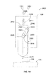
- FIG 15 is a perspective view of a connector system 1200 in accordance with another embodiment.
- the connector system 1200 includes first and second connectors 1202, 1204 that mate with each other.
- the connectors 1202, 1204 include contacts 1206, 1304 (shown in Figure 16 ) that engage each other when the connectors 1202, 1204 mate to electrically communicate data and/or power between the connectors 1202, 1204.
- the first connector 1202 includes a body 1208 that is coupled with a mating array 1210.
- the body 1208 may be a housing of an electronic device that uses the contacts 1206 to electrically communicate data and/or power with the connector 1204.
- the mating array 1210 includes an approximately planar substrate 1212 with the contacts 1206 joined to or supported by the substrate 1212.
- the planar substrate 1212 may be a printed circuit board.
- the planar substrate 1212 may be a printed circuit board having the contacts 1206 mounted to or part of the printed circuit board.
- the planar substrate 1212 may include or be adjacent to a flexible or compressive backing material (not shown).
- a backing material may permit the planar substrate 1212 to align itself with the second connector 1204 in order to account for any misalignment between the planar substrate 1212 and the second connector 1204.
- the backing material may permit the planar substrate 1212 to move such that the planar substrate 1212 is co-planar with the second connector 1204.
- the second connector 1204 is a circuit board, such as a printed circuit board.
- the second connector 1204 may be a different device or assembly that includes the contacts 1304 that mate with the contacts 1206 of the first connector 1202.
- rotating arms 1214 join the mating array 1210 to the body 1208.
- the arms 1214 are four elongated arms located at the corners of the mating array 1210. Alternatively, a different number of arms 1214 may be provided and/or the arms 1214 may be joined elsewhere to the mating array 1210.
- the rotating arms 1214 separate the mating array 1210 from the body 1208 such that a gap 1216 exists between the body 1208 and the mating array 1210.
- the arms 1214 rotate along respective arcs 1218 8 to move the mating array 1210 closer to or farther from the body 1208. For example, the arms 1214 may rotate toward the body 1208 to move the mating array 1210 toward the body 1208 and reduce the size of the gap 1216 between the body 1208 and the mating array 1210.
- the arms 1214 may rotate away from the body 1208 to move the mating array 1210 away from the body 1208 and increase the size of the gap 1216.
- the arms 1214 include or are coupled with resilient bodies (not shown), such as springs, that are compressed when the arms 1214 rotate toward the body 1208.
- the arms 1214 may include or be joined with torsion springs that are loaded when a compressive force 1220 is applied to the mating array 1210 in a direction toward the body 1208.
- the compressive force 1220 causes the mating array 1210 to move toward the body 1208 and the arms 1214 to rotate toward the body 1208.
- the loaded torsion springs apply a resistive force on the arms 1214 in an opposite direction of the compressive force 1220.
- the resistive force rotates the arms 1214 away from the body 1208 and moves the mating array 1210 away from the body 1208 when the compressive force 1220 is removed or sufficiently reduced.
- the resilient bodies of the arms 1214 may keep the mating array 1210 separated from the body 1208 when the first and second connectors 1202, 1204 are not mated with each other.
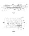
- Figure 16 is a cross-sectional view of the connector system 1200 in an unmated state along line A-A in Figure 15.
- Figure 17 is a detail view of a portion 1300 of the connector system 1200 shown in Figure 16 .
- the connectors 1202, 1204 are shown in Figures 13 and 14 as being separated from one another in an unmated state.
- the contacts 1206 of the first connector 1202 are coupled with the substrate 1212 of the mating array 1210.
- the substrate 1212 is a flexible member that may bend or flex in response to forces that are applied to the contacts 1206 and/or substrate 1212.
- the substrate 1212 may be flexible in order to permit the contacts 1206 to mate with irregular or non-planar mating surfaces.
- the contacts 1206 are presented on a mating side 1302 of the substrate 1212. As described above, the contacts 1206 engage pairing contacts 1304 on a surface 1306 of the second connector 1204.
- the contacts 1304 of the second connector 1204 may be substantially flat conductive elements, such as conductive pads formed on the surface 1306.
- the mating array 1210 includes several resilient members 1308 presented on the opposite side 1310 of the substrate 1212.
- the resilient members 1308 may be mounted to the side 1310 of the substrate 1212 that is opposite of the mating side 1302.
- one resilient member 1308 is provided for each contact 1206 of the mating array 1210.
- one resilient member 1308 may be provided for several contacts 1206 or more than one resilient member 1308 may be provided for each contact 1206.
- a single resilient member 1308, such as a sheet of resilient material, maybe disposed on the opposite side 1310 of the substrate 1212.
- the resilient members 1308 are bodies that are capable of being compressed between the mating array 1210 and the body 1208 when the connectors 1202, 1204 mate with each other and the mating array 1210 is moved toward the body 1208 of the first connector 1202.
- the resilient members 1308 include or are formed from a polymer that can be compressed.
- the resilient members 1308 may be springs that are compressed between the mating array 1210 and the body 1208.
- the resilient members 1308 may be spring fingers that are compressed between the mating array 1210 and the body 1208.
- Other alternative forms and compositions of the resilient members 1308 may be used.
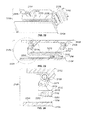
- Figure 18 is a cross-sectional view of the connector system 1200 in a partially mated state along line A-A in Figure 15 .
- Figure 19 is a detail view of a portion 1700 of the connector system 1200 shown in Figure 18 .
- the first connector 1202 mates with the second connector 1204 by moving the first and/or second connectors 1202, 1204 toward each other.
- the connectors 1202, 1204 may be moved such that the first connector 1202 moves relative to the second connector 1204 along the mating direction 1502.
- Once the contacts 1206 of the first connector 1202 engage the contacts 1304 of the second connector 1204, further movement of the first connector 1202 relative to the second connector 1204 in the mating direction 1502 causes the mating array 1210 to be pushed toward the body 1208 of the first connector 1202.
- the arms 1214 rotate toward the body 1208.
- the rotation of the arms 1214 toward the body 1208 causes the mating array 1210 and the contacts 1206 of the first connector 1202 to move in a wiping direction 1702 relative to the contacts 1304 of the second connector 1204.
- the mating direction 1502 in which the first connector 1202 moves relative to the second connector 1204 is approximately perpendicular to the lateral wiping direction 1702 in which the contacts 1206 of the first connector 1202 move relative to the contacts 1304 of the second connector 1204.
- the contacts 1206 are moving relative to the contacts 1304 in the wiping direction 1702.
- Figure 20 is a cross-sectional view of the connector system 1200 in a mated state along line A-A in Figure 15 .
- Figure 21 is a detail view of a portion 1900 of the connector system 1200 shown in Figure 20 .
- the connectors 1202, 1204 are shown mated with each other in Figures 17 and 18 .
- movement of the first connector 1202 along the mating direction 1502 relative to the second connector 1204 causes the mating array 1210 and the contacts 1206 of the first connector 1202 to wipe across the contacts 1304 of the second connector 1204 in the wiping direction 1702.
- the lateral movement of the contacts 1206 across the contacts 1304 may remove one or more layers of surface contamination on the contacts 1304 such that the contacts 1206, 1304 are electrically coupled with one another.
- the contacts 1206 may wipe across the contacts 1304 such that the electrical connection between the contacts 1206 and the contacts 1304 is improved over contacts 1206 that do not wipe across the contacts 1304.
- the resilient members 1308 may be compressed between the mating array 1210 and the body 1208 of the first connector 1202. Compression of the resilient members 1308 may provide increased tolerance in the location of the mating array 1210 such that the mating array 1210 may be moved toward the body 1208 to wipe the contacts 1206 across the contact 1304 while avoiding bottoming out or abutting the body 1208.
- the resilient members 1308 may account for undulations and uneven locations of the contacts 1304 relative to the contacts 1206.
- the arms 1214 may include or be coupled with resilient bodies such as springs that cause the arms 1214 to rotate away from the body 1208 and the mating array 1210 to move away from the body 1208 when the first and second connectors 1202, 1204 move away from each other.
- the mating array 1210 may return to the position shown in Figures 13 and 14 when the first and second connectors 1202, 1204 are moved away from each other.
- FIG 22 is a perspective view of a connector system 2100 in accordance with another embodiment.
- the connector system 2100 includes first and second connectors 2102, 2104 that mate with each other.
- the connector 2104 may be referred to as a mating connector. Similar to the connector system 1200 (shown in Figure 15 ), the connectors 2102, 2104 include contacts 2106, 2204 (shown in Figure 23 ) that engage each other when the connectors 2102, 2104 mate to electrically communicate data and/or power between the connectors 2102, 2104.
- the first connector 2102 includes a body 2108 that is coupled with a mating array 2110. Similar to the body 1208 (shown in Figure 15 ), the body 2108 may be a housing of an electronic device.
- the mating array 2110 includes an approximately planar substrate 2112 with the contacts 2106 joined to the substrate 2112.
- the second connector 2104 may be a circuit board or other device or assembly that includes the contacts 2204 that mate with the contacts 2106 of the first connector 2102.
- the first connector 2102 includes rotating arms 2114 that join the mating array 2110 to the body 2108.
- the rotating arms 2114 are two hinge elements that are joined to opposite sides of the mating array 2110.
- a different number of rotating arms 2114 may be provided and/or the rotating arms 2114 may be joined to the mating array 2110 in different locations.
- the rotating arms 2114 separate the mating array 2110 from the body 2108.
- the rotating arms 2114 rotate along respective arcs 2118 to move the mating array 2110 closer to or farther from the body 2108, similar to as described above in connection with the arms 1214 of the first connector 1202 shown in Figure 15 .
- Figure 23 is a cross-sectional view of the connector system 2100 in an unmated state along line B-B in Figure 22.
- Figure 24 is a detail view of a portion 2200 of the connector system 2100 shown in Figure 23 .
- the substrate 2112 is a flexible member that may bend or flex in response to forces that are applied to the contacts 2106 and/or substrate 2112.
- the contacts 2106 are presented on a mating side 2202 of the mating array 2110.
- the contacts 2106 engage pairing contacts 2204 on a surface 2206 of the second connector 2104.
- the contacts 2204 of the second connector 2104 may be similar to the contacts 1304 (shown in Figure 15 ) of the second connector 1204 (shown in Figure 15 ).
- the mating array 2110 includes an opposite side 2210 that faces the body 2108 of the first connector 2102.
- resilient bodies 2214 are disposed within the rotating arms 2114.
- the resilient bodies 2214 shown in Figures 20 and 21 are torsion springs, but alternatively may be a different resilient body.
- the resilient bodies 2214 are compressed when the rotating arms 2114 rotate toward the body 2108.
- the resilient bodies 2214 may be compressed when the mating array 2110 engages the second connector 2104 and is forced toward the body 2108.
- the rotating arms 2114 may rotate toward the body 2108.
- the resilient bodies 2214 are compressed.
- Figure 25 is a cross-sectional view of the connector system 2100 in a partially mated state along line B-B in Figure 22 .
- Figure 26 is a detail view of a portion 2400 of the connector system 2100 shown in Figure 25 .
- the first connector 2102 mates with the second connector 2104 by moving the first and/or second connectors 2102, 2104 toward each other.
- the connectors 2102, 2104 may be moved such that the first connector 2102 moves relative to the second connector 2104 along a mating direction 2402.
- the contacts 2106 of the first connector 2102 when the contacts 2106 of the first connector 2102 initially engage the contacts 2204 of the second connector 2104, the contacts 2106, 2204 may not be aligned with each other.
- the mating array 2110 may move toward the body 2108 of the first connector 2102.
- the mating array 2110 may be pushed toward the body 2108 such that the rotating arms 2114 rotate toward the body 2108.
- Figure 27 is a cross-sectional view of the connector system 2100 in a mated state along line B-B in Figure 22 .
- Figure 28 is a detail view of a portion 2600 of the connector system 2100 shown in Figure 27 .
- the first connector 2102 mates with the second connector 2104 by moving the first and/or second connectors 2102, 2104 toward each other.
- the connectors 2102, 2104 may be moved such that the first connector 2102 moves relative to the second connector 2104 along the mating direction 2402.
- the mating array 2110 is pushed toward the body 2108 of the first connector 2102.
- the rotating arms 2114 rotate toward the body 2108.
- the rotation of the rotating arms 2114 causes the mating array 2110 and the contacts 2106 of the first connector 2102 to move in a wiping direction 2602 relative to the contacts 2204 of the second connector 2104.
- the mating direction 2402 may be approximately perpendicular to the lateral wiping direction 2602.
- the lateral movement of the contacts 2106 across the contacts 2204 may remove one or more layers of surface contamination on the contacts 2204 such that the contacts 2106, 2204 are electrically coupled with one another.
- the contacts 2106 may wipe across the contacts 2204 such that the electrical connection between the contacts 2106 and the contacts 2204 is improved over contacts 2106 that do not wipe across the contacts 2204.
- the resilient bodies 2214 are compressed between the rotating arms 2114 and the body 2108 when the connectors 2102, 2104 are mated.
- the compression of the resilient bodies 2214 causes the resilient bodies 2214 to exert forces on the mating array.
- the forces exerted by the resilient bodies 2214 may cause the mating array 2110 to move away from the body 2108 and return to the position shown in Figures 20 and 21 .
Landscapes
- Coupling Device And Connection With Printed Circuit (AREA)
- Details Of Connecting Devices For Male And Female Coupling (AREA)
Abstract
A connector (102) comprises a housing (112) and a contact (106) coupled with the housing (112). The contact (106) has a mating end (300) and an interface end (302). An angled interface (318) is disposed within the housing (112) and arranged for sliding engagement with the interface end (302) of the contact (106). When the housing (112) is moved in a mating direction (110) toward a mating connector (104) and the mating end (300) of the contact (106) engages a conductive element (108) of the mating connector (104) further movement of the housing (112) in the mating direction (110) causes the interface end (302) of the contact (106) to slidably move along the angled interface (318), whereby the angled interface (318) imparts translational movement of the contact (106) with respect to the housing (112) and the mating end (300) of the contact (106) moves laterally across the conductive element (108).
Description
- The invention relates to an electrical connector having a contact that engages a contact pad of a mating connector.
- Known electrical connectors include contacts disposed within or coupled with a housing. The housings mate with one another to electrically couple the contacts. Once the contacts are joined with one another, the connectors communicate data signals and/or power between each other via the coupled contacts. Some known connectors include contacts that mate with contact pads of another connector. For example, a connector system may include a first connector that includes several contacts while a second connector includes several substantially flat contact pads. By way of example only, the second connector may be a printed circuit board that includes contact pads disposed on one side of the board. The contacts engage the contact pads to electrically couple the contacts with the contact pads.
- The contact pads may include or be formed from metals or metal alloys that may develop an insulating layer of surface contamination when exposed to the environment over time. This layer may be present on the surface of the contact pads that mate with the first connector. The layer may negatively impact the coupling between the connector and the contact pads. For example, the layer may have a greater resistivity than the contact pad and increase the resistance of the coupling between the contacts and the contact pads.
- In order to improve the electrical coupling between the contacts and the contact pads, the layer of surface contamination may be locally removed from the contact pad by laterally moving the contact across the surface of the contact pad. The lateral movement of the contact may scrape off or otherwise remove the layer of surface contamination from a portion of the contact pad. The contact engages the contact pad where the layer has been removed for an improved electrical coupling between the contact and the contact pad.
- But, with some known connectors, in order to laterally move the contact across the contact pad and remove the layer of surface contamination, the connector in which the contact is disposed must be laterally moved with respect to the connector that includes the contact pad. In some applications, there is insufficient room to laterally move the connectors relative to each other. Additionally, lateral movement of the connectors relative to each other may result in misalignment of the contacts relative to the contact pads. Such misalignment may prevent some of the contacts from mating with the contact pads.
- There is a need for a connector that can mate with another connector having a contact pad while removing a layer of surface contamination from the contact pad.
- This problem is solved a connector according to claim 1.
- According to the invention, a connector comprises a housing and a contact coupled with the housing. The contact has a mating end and an interface end. An angled interface is disposed within the housing and arranged for sliding engagement with the interface end of the contact. When the housing is moved in a mating direction toward a mating connector and the mating end of the contact engages a conductive element of the mating connector, further movement of the housing in the mating direction causes the interface end of the contact to slidably move along the angled interface, whereby the angled interface imparts translational movement of the contact with respect to the housing and the mating end of the contact moves laterally across the conductive element.
- The invention will now be described by way of example with reference to the accompanying drawings wherein:
-
Figure 1 is an elevational view of a decoupled connector system in accordance with one embodiment of the present disclosure. -
Figure 2 is an elevational view of a coupled or mated connector system in accordance with one embodiment of the present disclosure. -
Figure 3 is an illustration of a front end of a connector shown inFigure 1 in accordance with one embodiment of the present disclosure. -
Figure 4 is a schematic illustration of a contact of the connector shown inFigure 1 in an initial position also shown inFigure 1 in accordance with one embodiment of the present disclosure. -
Figure 5 is a schematic illustration of the contact shown inFigure 1 in a mated position shown inFigure 2 in accordance with one embodiment of the present disclosure. -
Figure 6 is a schematic illustration of a contact disposed within the connector shown inFigure 1 in an initial position in accordance with an alternative embodiment of the present disclosure. -
Figure 7 is a schematic illustration of the contact shown inFigure 6 disposed within the connector shown inFigure 1 in a subsequent mated position in accordance with one embodiment of the present disclosure. -
Figure 8 is a schematic illustration of a contact in a connector in an initial position in accordance with an alternative embodiment of the present disclosure. -
Figure 9 is a schematic illustration of the contact shown inFigure 8 disposed within the connector shown inFigure 8 in a mated position. -
Figure 10 is a schematic illustration of a contact disposed within a connector in an initial position in accordance with an alternative embodiment of the present disclosure. -
Figure 11 is a schematic illustration of a contact disposed within a connector in an initial position in accordance with an alternative embodiment of the present disclosure. -
Figure 12 is a schematic illustration of a contact in an initial position within a connector in accordance with an alternative embodiment of the present disclosure. -
Figure 13 is a schematic illustration of the contact (shown inFigure 12 ) of the connector (shown inFigure 12 ) in a mated position in accordance with one embodiment of the present disclosure. -
Figure 14 is a schematic illustration of a contact disposed within a connector in an initial position in accordance with an alternative embodiment of the present disclosure. -
Figure 15 is a perspective view of a connector system in accordance with another embodiment. -
Figure 16 is a cross-sectional view of the connector system shown inFigure 15 in an unmated state along line A-A inFigure 15 . -
Figure 17 is a detail view of a portion of the connector system shown inFigure 16 . -
Figure 18 is a cross-sectional view of the connector system shown inFigure 15 in a partially mated state along line A-A inFigure 15 . -
Figure 19 is a detail view of a portion of the connector system shown inFigure 18 . -
Figure 20 is a cross-sectional view of the connector system shown inFigure 15 in a mated state along line A-A inFigure 15 . -
Figure 21 is a detail view of a portion of the connector system shown inFigure 20 . -
Figure 22 is a perspective view of a connector system in accordance with another embodiment. -
Figure 23 is a cross-sectional view of the connector system shown inFigure 22 in an unmated state along line B-B inFigure 22 . -
Figure 24 is a detail view of a portion of the connector system shown inFigure 23 . -
Figure 25 is a cross-sectional view of the connector system shown inFigure 22 in a partially mated state along line B-B inFigure 22 . -
Figure 26 is a detail view of a portion of the connector system shown inFigure 25 . -
Figure 27 is a cross-sectional view of the connector system shown inFigure 22 in a mated state along line B-B inFigure 22 . -
Figure 28 is a detail view of a portion of the connector system shown inFigure 27 . -
Figure 1 is an elevational view of a decoupledconnector system 100 in accordance with one embodiment of the present disclosure.Figure 2 is an elevational view of a coupled ormated connector system 100 in accordance with one embodiment of the present disclosure. Thesystem 100 includes twoconnectors connectors connector 104 may be referred to herein as a mating connector. Thefirst connector 102 includes ahousing 112 that extends from afront end 114 to aback end 116.Several contacts 106 are disposed within thehousing 112 and protrude from thefront end 114. Alternatively, thecontacts 106 may be recessed within thehousing 112 such that thecontacts 106 do not protrude from thefront end 114. The number ofcontacts 106 shown inFigures 1 and 2 is provided merely as an example. - The
contacts 106 engage correspondingconductive elements 108 of thesecond connector 104. Thecontact 106 and theconductive element 108 include, or are formed from, conductive materials, such as metals or metal alloys. In one embodiment, thecontacts 106 of thefirst connector 102 are elongated contacts. Alternatively, thecontacts 106 may be non-elongated contacts. For example, thecontacts 106 may not be elongated in amating direction 110 that thefirst connector 102 and/orsecond connector 104 are moved relative to each other. The second, or mating,connector 104 may be a circuit board, such as a printed circuit board (PCB), with theconductive elements 108 being contacts that mate with thecontacts 106. Theconductive elements 108 may be substantially flat contact pads disposed on one side of the circuit board. The number ofconductive elements 108 is shown merely as an example. Alternatively, thesecond connector 104 may be a connector other than a circuit board. - The
connectors first connector 102 toward thesecond connector 104 in themating direction 110 or by moving thesecond connector 104 in a direction that is opposite of themating direction 110 until thecontacts 106 of thefirst connector 102 engage theconductive elements 108 of thesecond connector 104. For example, at least one of theconnectors connectors Figure 1 , themating direction 110 is oriented approximately parallel to alongitudinal axis 304 of thecontact 106. Prior to mating theconnectors contacts 106 is located at aninitial position 118 at thefront end 114 of thehousing 112. The spacing between theinitial positions 118 ofadjacent contacts 106 may be uniform or non-uniform across thefront end 114. Theinitial position 118 of eachcontact 106 may correspond to the location of thelongitudinal axis 304 of thecontact 106 along thefront end 114. Theconductive elements 108 of thesecond connector 104 may have center lines or axes 120 that extend through the center of theconductive elements 108. As shown inFigure 1 , thelongitudinal axes 304 of thecontacts 106 are laterally spaced apart from the center axes 120 of theconductive elements 108. For example, thelongitudinal axis 304 of acontact 106 and thecenter axis 120 of aconductive element 108 that mates with thecontact 106 may be spaced apart by alateral gap 122 along a direction that is transverse or perpendicular to thelongitudinal axis 304. - When the
connectors contacts 106 are caused to move laterally across theconductive elements 108 as will be explained in more detail hereinbelow. For example, as shown inFigure 2 , thecontacts 106 wipe across the upper surfaces of theconductive elements 108 in wipingdirections mating direction 110. Somecontacts 106 may move in the wipingdirection 200A whileother contacts 106 move in the wipingdirection 200B toward the center axes 120 of theconductive elements 108. Different subsets of thecontacts 106 in the array may move indifferent wiping directions direction 200A of one subset ofcontacts 106 may be oriented opposite of the wipingdirection 200B of another subset ofcontacts 106. Alternatively, all of thecontacts 106 may move in acommon wiping direction contacts 106 laterally move in thewiping directions initial positions 118 to mated positions 202 (shown inFigure 2 ). Thecontacts 106 are laterally displaced by alateral distance 204 when theconnectors lateral distance 204 is approximately the same as the lateral gap 122 (shown inFigure 1 ) between theinitial positions 118 of thecontacts 106 and the center axes 120 of theconductive elements 108 such that thelongitudinal axes 304 of thecontacts 106 are aligned with the center axes 120 of theconductive elements 108. Thecontacts 106 may move in the wipingdirection 200 relative to theconnectors connectors connectors mating direction 110 while thecontacts 106 simultaneously or concurrently move in thelateral wiping directions - The
contacts 106 may move in thewiping directions connector 102 to prevent misalignment of thecontacts 106 with theconductive elements 108. For example, if thecontacts 106 were able to laterally move across theconductive elements 108 only if theconnector 102 also moved in the wipingdirection contacts 106 may become misaligned with theconductive elements 108. The independent lateral movement of thecontacts 106 permits an operator to align theconnectors mating direction 110 while still achieving a wiping motion of thecontacts 106 across theconductive elements 108 in thewiping directions - The wiping movement of the
contacts 106 across theconductive elements 108 may improve an electrical coupling between thecontacts 106 andconductive elements 108. For example, the wiping movement of thecontacts 106 across theconductive elements 108 may remove one or more layers of surface contamination on theconductive elements 108. Removal of the surface contamination may reduce the resistivity of the coupling between thecontacts 106 andconductive elements 108. - As shown in
Figures 1 and 2 , thecontacts 106 laterally move in thewiping directions housing 112 of theconnector 102 and theconnector 104. For example, thecontacts 106 move within thehousing 112 without thehousing 112 laterally moving with respect to theconnector 104. Thecontacts 106 may return to theinitial positions 118 when theconnectors connector 102 may be retreated away from theconnector 104 in a decoupling direction 206 (shown inFigure 2 ) to separate thecontacts 106 andconductive elements 108 from one another and break the electrical coupling between thecontacts 106 andconductive elements 108. As theconnector 102 moves away from theconnector 104 in thedecoupling direction 206, thecontacts 106 return to theinitial positions 118 as shown inFigure 1 . For example, thecontacts 106 may laterally move within and relative to thehousing 112 back to theinitial positions 118. -
Figure 3 is an illustration of thefront end 114 of theconnector 102 in accordance with one embodiment of the present disclosure.Channels 310 may be arranged in an array across thefront end 114. Each of thechannels 310 is bounded by opposingend walls side walls channels 310 includecontacts 106 that protrude from thefront end 114. Thecontacts 106 move in thewiping directions channels 310 during mating of theconnector 102 with theconnector 104. In the illustrated embodiment, different subsets of thecontacts 106 move indifferent wiping directions contacts 106 may move in awiping direction 200A from thewall 312 toward thewall 314 whileother contacts 106 move in awiping direction 200B from thewall 314 toward thewall 312. Thechannels 310 may extend inward from thefront end 114 to defineopenings 700 along thefront end 114. Theopenings 700 are elongated in directions parallel to thewiping directions - The
openings 700 have awidth dimension 702 in a direction that is angled with respect to thecorresponding wiping direction width dimension 702 may extend in a direction that is perpendicular to the wipingdirection contact 106 in thechannel 310. Thewidth dimension 702 may be sufficiently large to permit movement of thecontacts 106 in the wipingdirection contacts 106 to the wipingdirection width dimension 702 may be slightly larger than awidth dimension 708 of thecontacts 106 to permit movement of thecontacts 106 in thewiping directions contacts 106 in directions that are angled with respect to thewiping directions -
Figure 4 is a schematic illustration of one of thecontacts 106 of theconnector 102 in the initial position 118 (shown inFigure 1 ) in accordance with one embodiment of the present disclosure.Figure 5 is a schematic illustration of thecontact 106 in the mated position 202 (shown inFigure 2 ) with respect to theconductive element 108 in accordance with one embodiment of the present disclosure. Thecontact 106 is disposed within achannel 310 of the housing 112 (shown inFigure 1 ). For example, thechannel 310 may be an interior section of thehousing 112 that is bounded by opposingend walls wall 316. As shown inFigures 4 and 5 , thechannel 310 is located inside thehousing 112 with the interconnectingwall 316 separated from theback end 116 of thehousing 112. Alternatively, the interconnectingwall 316 and theback end 116 may be the same component or portion of thehousing 112. - The
front end 114 of thehousing 112 opposes the interconnectingwall 316. Thecontact 106 may be an elongated contact that extends from aninterface end 302 to amating end 300 along thelongitudinal axis 304. Alternatively, thecontact 106 may be a non-elongated contact. For example, thecontact 106 may not be longer between theinterface end 302 and themating end 300 than in another direction. While themating end 300 is shown as a rounded tip, alternatively themating end 300 may have a different shape. The illustratedinterface end 302 includessides sides sides longitudinal axis 304. In the illustrated embodiment, thesides longitudinal axis 304. In another embodiment, one or more of thesides longitudinal axis 304. Alternatively, theinterface end 302 includes only theside 306. In another embodiment, theinterface end 302 may be rounded in a manner similar to themating end 300. - The
channel 310 includes anangled interface 318 that is angled with respect to thelongitudinal axis 304 of thecontact 106. For example, theangled interface 318 may include a slidingsurface 320 that is obliquely oriented with respect to thelongitudinal axis 304. The slidingsurface 320 may be oriented at anangle 328 with respect to thelongitudinal axis 304. As shown inFigures 4 and 5 , theangle 328 is an acute angle of approximately 45 degrees. Alternatively, theangle 328 may be a different angle, such as 30 degrees. The slidingsurface 320 may include or be formed from a conductive material, such as one or more metals or metal alloys. Theangled interface 318 and/or slidingsurface 320 may be electrically coupled with a source or recipient (not shown) of the data and/or power that is electrically communicated between theconnectors surface 320 may be a contact pad similar to theconductive element 108 that receives data signals communicated from theconnector 104 to theconnector 102 via thecontacts 106 andconductive elements 108. - The
angled interface 318 is slidably coupled with theinterface end 302 of thecontact 106. For example, theangled interface 318 may slidably engage one of thesides interface end 302. Theinterface end 302 may remain electrically coupled with theangled interface 318 while theinterface end 302 slides along theangled interface 318. For example, a conductive pathway that communicates data and/or power between theconnectors contact 106 may extend across the interface between the slidingsurface 320 and theinterface end 302 of thecontact 106. In the illustrated embodiment, theside 306 of thecontact 106 includes acoating 322 that is disposed between theside 306 and theangled interface 318. Thecoating 322 may include, or be formed from, one or more conductive materials. Thecoating 322 may be formed of a material that reduces the coefficient of friction between theside 306 and the slidingsurface 320 to permit theinterface end 302 to slide more easily along theangled interface 318. - As shown in
Figures 4 and 5 , theinterface end 302 of thecontact 106 slides along theangled interface 318 as theconnector 102 is moved in themating direction 110 to mate with theconnector 104. For example, when thelongitudinal axis 304 of thecontact 106 is in the initial position 118 (which may be separated from thecenter axis 120 of the conductive element 108), theside 306 is located in an initial position along the slidingsurface 320 of theangled interface 318. When theconnector 102 is moved in themating direction 110 toward theconnector 104, themating end 300 of thecontact 106 engages theconductive element 108. In one embodiment, after themating end 300 abuts theconductive element 108, continued movement of theconnector 102 in themating direction 110 may cause thecontact 106 to slide along theangled interface 318. For example, the continued movement of theconnector 102 in themating direction 110 may impart a force on theconductive element 108 in themating direction 110 and an approximately equal and opposite force in an opposite direction. The force in the opposite direction is applied by theinterface end 302 of thecontact 106 onto theangled interface 318. The angled orientation of theangled interface 318 with respect to thecontact 106 may translate the force applied by thecontact 106 onto theangled interface 318 into a sliding movement of thecontact 106 along theangled interface 318. For example, theside 306 of thecontact 106 may slide along the slidingsurface 320 in a sliding direction 400 (shown inFigure 5 ). - The movement of the
contact 106 in the slidingdirection 400 laterally displaces thecontact 106 with respect to theconductive element 108. As shown inFigure 5 , the movement of theinterface end 302 of thecontact 106 along theangled interface 318 in the slidingdirection 400 also moves themating end 300 of thecontact 106 in the wipingdirection 200A across theconductive element 108. Alternatively, thecontact 106 may move in the wipingdirection 200B (shown inFigure 2 ). Thecontact 106 may move in the wipingdirection 200A such that thelongitudinal axis 304 of thecontact 106 is aligned with thecenter axis 120 of theconductive element 108. Alternatively, thecontact 106 may move such that thelongitudinal axis 304 of thecontact 106 moves toward thecenter axis 120 of theconductive element 108, but is not aligned with thecenter axis 120. The wipingdirection 200A may be laterally oriented with respect to themating direction 110. For example, the movement of theconnector 102 in themating direction 110 may cause thecontact 106 to simultaneously move across theconductive element 108 in the wipingdirection 200A. The engagement between theangled interface 318 in theconnector 102 and theinterface end 302 of thecontact 106 may translate the movement of thecontact 106 and theconnector 102 in themating direction 110 into lateral movement of thecontact 106 in the wipingdirection 200A while theconnector 102 continues to move in themating direction 110. Thecontact 106 moves in the wipingdirection 200A to the matedposition 202. Thecontact 106 may move in the wipingdirection 200A relative to theconductive element 108 without any lateral movement of theconnectors - In one embodiment, the
connector 102 includes aresilient member 324 that is coupled with thecontact 106. Theresilient member 324 may be joined to thecontact 106 between theends resilient member 324 is perpendicularly oriented with respect to thelongitudinal axis 304, alternatively theresilient member 324 may be obliquely oriented with respect to thelongitudinal axis 304. Theresilient member 324 is a body that applies a force 404 (shown inFigure 5 ) onto thecontact 106 when theresilient member 324 is compressed. For example, theresilient member 324 may be a spring that extends between thecontact 106 and aninterior wall 326 in thechannel 310. Compression of theresilient member 324 may impart theforce 404 on thecontact 106. Theresilient member 324 may have an uncompressed length that extends from thecontact 106 to theinterior wall 326 in a perpendicular direction with respect to thelongitudinal axis 304 when thecontact 106 is decoupled from theconductive element 108. Theresilient member 324 is compressed to a shorter compressed length when theconnectors contact 106 laterally moves in the wipingdirection 200A, as described above. - The
resilient member 324 is compressed between thecontact 106 and theinterior wall 326 when thecontact 106 moves in the wipingdirection 200A from the initial position 118 (shown inFigure 1 ). The movement of thecontact 106 in the wipingdirection 200A opposes theforce 404 applied by theresilient member 324. Additionally, theforce 404 may return thecontact 106 to theinitial position 118 when theconnectors resilient member 324 moves thecontact 106 from the matedposition 202 to theinitial position 118 when theconnectors - The
connector 102 may be decoupled from theconnector 104 by moving theconnector 102 in a direction opposite of themating direction 110. As theconnector 102 is retreated away from theconnector 104 and thecontact 106 is retreated away from theconductive element 108, the compressedresilient member 324 continues to apply theforce 404 on thecontact 106. Theresilient member 324 may apply theforce 404 until theresilient member 324 is no longer compressed, or until thecontact 106 is returned to theinitial position 118. The application of theforce 404 pushes thecontact 106 in a lateral direction that opposes the wipingdirection 200A. For example, as theforce 404 is applied to thecontact 106, theinterface end 302 of thecontact 106 may slide down theangled interface 318 in a direction that opposes the slidingdirection 400. For example, thecontact 106 may slide along theangled interface 318 from the position shown inFigure 5 to the position shown inFigure 4 . Theresilient member 324 returns thecontact 106 to theinitial position 118 so that theside 306 may move in the slidingdirection 400 along theangled interface 318 the next time theconnectors contact 106 across theconductive element 108, as described above. -
Figure 6 is a schematic illustration of acontact 500 disposed within theconnector 102 in an initial position in accordance with an alternative embodiment of the present disclosure.Figure 7 is a schematic illustration of thecontact 500 disposed within theconnector 102 in a subsequent mated position in accordance with one embodiment of the present disclosure. Thecontact 500 may be disposed within achannel 502 similar to the contact 106 (shown inFigure 1 ) in the channel 310 (shown inFigure 3 ). Thecontact 500 may be an elongated contact that is divided into multiple sections, including a slidingsection 504 and amating section 506 separated from one another by a gap. Alternatively, thecontact 500 may be a non-elongated contact. While twosections contact 500 may be divided into a greater number of sections. Thesections longitudinal axis 508 of thecontact 500. Themating section 506 extends from aninternal end 512 to amating end 510 along thelongitudinal axis 508. The slidingsection 504 extends between anotherinternal end 514 and aninterface end 516 along thelongitudinal axis 508. While themating end 510 is shown as a rounded tip, alternatively themating end 510 may have a different shape. Similar to the interface end 302 (shown inFigure 4 ), the illustratedinterface end 516 includessides - As shown in
Figures 6 and 7 , thechannel 502 is located inside thehousing 112. Similar to the channel 310 (shown inFigure 3 ), thechannel 502 includes anangled interface 522 that is angled with respect to thelongitudinal axis 508. Theangled interface 522 may include a slidingsurface 524 that is obliquely oriented with respect to thelongitudinal axis 508. The slidingsurface 524 may be oriented at anangle 542 with respect to thelongitudinal axis 508. As shown inFigures 6 and 7 , theangle 542 is an acute angle of approximately 45 degrees. Alternatively, theangle 542 may be a different angle, such as 30 degrees. The slidingsurface 524 may include or be formed from a conductive material, such as one or more metals or metal alloys. Theangled interface 522 and/or slidingsurface 524 may be electrically coupled with a source or recipient (not shown) of the data and/or power that is electrically communicated between theconnectors - The
angled interface 522 is slidably coupled with theinterface end 516 of thecontact 500. Theinterface end 516 may remain electrically coupled with theangled interface 522 while theinterface end 516 slides along theangled interface 522. In the illustrated embodiment, theside 518 includes acoating 526 that may be similar to the coating 322 (shown inFigure 4 ). Similar to the contact 106 (shown inFigure 5 ), theinterface end 516 of thecontact 500 slides along theangled interface 522 as theconnector 102 mates with theconnector 104 along themating direction 110. Prior to mating thecontact 500 with theconductive element 108, thelongitudinal axis 508 of thecontact 500 is located at theinitial position 118 that is laterally spaced apart from thecenter axis 120 of theconductive element 108. As thecontact 500 mates with theconductive element 108 and slides along theangled interface 522, thecontact 500 laterally moves across theconductive element 108 such that thelongitudinal axis 508 moves toward thecenter axis 120 of theconductive element 108. For example, thecontact 500 may move such that the longitudinal and center axes 508, 120 are aligned. Alternatively, thecontact 500 may move such that thelongitudinal axis 508 moves toward thecenter axis 120 but is not aligned with thecenter axis 120. The pitch of theangled interface 522 relative to thelongitudinal axis 508 translates the movement of thecontact 500 in themating direction 110 to lateral movement across theconductive element 108 in the wipingdirection 200A, similar to as described above. - One difference between the contacts 106 (shown in
Figure 1 ) and 500 is the addition of one or more additional resilient members. For example, in contrast to thecontact 106, thecontact 500 is coupled with an upperresilient member 530 and a lowerresilient member 532. The upperresilient member 530 is coupled with the slidingsection 504 of thecontact 500 and extends from the slidingsection 504 to aninterior wall 534 that is similar to the interior wall 326 (shown inFigure 4 ). The lowerresilient member 532 is coupled to themating section 506 and extends from themating section 506 to theinterior wall 534. Similar to the resilient member 324 (shown inFigure 4 ), theresilient members contact 500 and theinterior wall 534 when thecontact 500 moves in the wipingdirection 200A during mating of theconnectors resilient members respective forces sections contact 500 when thecontact 500 moves in the wipingdirection 200A. As described above, theforces contact 500 in a lateral direction oriented opposite of the wipingdirection 200A when theconnector 102 retreats away from and decouples from theconnector 104. The inclusion of multipleresilient members contact 500 along the wipingdirection 200A. For example, the multipleresilient members forces contact 500 between theends - The
sections contact 500 may be interconnected by a normalresilient member 528. In the illustrated embodiment, the normalresilient member 528 is disposed within the gap between thesections resilient member 528 may be located within thecontact 500. For example, one of thesections sections longitudinal axis 508 with the normalresilient member 528 disposed between thesections resilient member 528 is a body that applies aforce 540 on themating section 506 when the normalresilient member 528 is compressed. For example, the normalresilient member 528 may be a spring disposed within thecontact 500 between thesections resilient member 528 may provide a force on themating section 506 in a direction parallel to themating direction 110 to ensure that themating end 510 remains engaged with theconductive element 108 during mating of theconnectors mating end 510 engages theconductive element 108 during mating of theconnectors connector 102 in themating direction 110 relative to theconnector 104 may displace thesections contact 500 in the wipingdirection 200A. The displacement of thesections resilient member 528. - As the normal
resilient member 528 is compressed, the normalresilient member 528 exerts amating force 540 on themating section 506 in a direction parallel to themating direction 110 to push themating section 506 along themating direction 110. Themating force 540 may ensure engagement between themating end 510 and theconductive element 108 as thecontact 500 wipes across theconductive element 108 in the wipingdirection 200A. For example, themating force 540 may push themating section 506 along themating direction 110 to maintain contact between themating end 510 and theconductive element 108 as thecontact 500 wipes across theconductive element 108. -
Figure 8 is a schematic illustration of acontact 800 disposed within aconnector 802 in an initial position in accordance with an alternative embodiment of the present disclosure. Only a portion of theconnector 802 is shown. Theconnector 802 may be similar to the connector 102 (shown inFigure 1 ) in that theconnector 802 may includeseveral channels 804 in whichseveral contacts 800 are disposed. Theconnector 802 includes aninterface 808 in thechannel 804. Theinterface 808 may include or be formed from a conductive material, such as one or more metals or metal alloys. Theinterface 808 may be electrically coupled with a source or recipient (not shown) of the data and/or power. Thecontact 800 is elongated along alongitudinal axis 806. Thecontact 800 extends between amating end 810 and aninterface end 812. Theinterface end 812 includes a resilientconductive member 814. The resilientconductive member 814 may be a wire or a spring such as an elongated torsion or return spring. Alternatively, thecontact 800 may have an angled side that is similar to the side 306 (shown inFigure 4 ). The resilientconductive member 814 engages theinterface 808 to electrically couple thecontact 800 with theinterface 808. As described below, themating end 810 wipes across theconductive element 108 of theconnector 104 when theconnector 800 mates with theconnector 104. - In the position shown in
Figure 8 , thelongitudinal axis 806 is located at aninitial position 828 that may be similar to the initial position 118 (shown inFigure 1 ) of the contacts 106 (shown inFigure 1 ). Thelongitudinal axis 806 is laterally spaced apart from thecenter axis 120 of theconductive element 108 prior to mating thecontact 800 with theconductive element 108. Theconnector 802 may include acam 816. Thecam 816 may be pivotally joined with theconnector 802 by apin 818. Thecam 816 may also be connected with anotherpin 820 that may be joined with thecontact 800. Aspring 822 may be joined to thecam 816 and to theconnector 802. In the illustrated embodiment, thespring 822 is joined at oneend 824 to thecam 816 and to theconnector 802 at anopposite end 826. Thespring 822 may be a helical spring such as a compression or torsion helical spring. - The
cam 816 pivots about thepin 818 when themating end 810 of thecontact 800 engages theconductive element 108. The pivoting of thecam 816 translates movement of thecontact 800 and theconnector 802 in themating direction 902 into lateral movement of thecontact 800 in the wipingdirection 904 across theconductive element 108. Thespring 822 imparts a restoring force on thecam 816 that causes thecam 816 to pivot about thepin 818 in an opposite direction when theconnector 802 moves away from theconnector 104. Alternatively, the resilientconductive member 814 provides the restoring force. -
Figure 9 is a schematic illustration of thecontact 800 disposed within theconnector 802 in a mated position. During mating of theconnectors contact 800 is moved toward theconductive element 108 along themating direction 902. When themating end 810 of thecontact 800 engages theconductive element 108, further movement of thecontact 800 toward theconductive element 108 causes thecontact 800 to move relative to theconnector 802 in adirection 906 that is opposite of themating direction 902. As thecontact 800 moves in thedirection 906, thecam 816 pivots about thepin 818 along anarcuate path 900. The pivoting of thecam 816 about thepin 818 causes thecontact 800 to laterally move relative to theconductive element 108. For example, the fixed length of thecam 816 may cause the movement of thecontact 800 in thedirection 906 to be translated into movement of thecontact 800 in awiping direction 904. Thecontact 800 moves in the wipingdirection 904 such that thelongitudinal axis 806 of thecontact 800 laterally moves from theinitial position 828 toward thecenter axis 120 of theconductive element 108. Thecontact 800 may move such that the longitudinal and center axes 806, 120 are aligned, or may move such that the longitudinal and center axes 806, 120 are not aligned. - The lateral movement of the
mating end 810 across theconductive element 108 in the wipingdirection 904 may remove one or more layers of surface contamination on theconductive element 108 to improve the electrical coupling of thecontact 800 with theconductive element 108. When theconnector 802 is decoupled from theconnector 104, thespring 822 may restore thecontact 800 from the position of thecontact 800 shown inFigure 9 to the position of thecontact 800 shown inFigure 8 . For example, mating thecontact 800 with theconductive element 108 and pivoting thecam 816 along thearcuate path 900 may compress thespring 822 between thecam 816 and theconnector 802. Moving thecontact 800 away from theconductive element 108 may permit thecompressed spring 822 to impart a restoring force on thecam 816. This restoring force may cause thecam 816 to pivot in an opposite direction along an oppositearcuate path 908. As thecam 816 pivots along thearcuate path 908, thecontact 800 may move to the position shown inFigure 8 . While thecam 816 in the illustrated embodiment translates movement of asingle contact 800 toward theconductive element 108 into lateral movement along the wipingdirection 904, alternatively thecam 816 may be joined withseveral contacts 800 in theconnector 802. Thecam 816 may then translate movement ofseveral contacts 800 toward respectiveconductive elements 108 into lateral movement of thecontacts 800 in the wipingdirection 904 to mate thecontacts 800 with theconductive elements 108 while wiping thecontacts 800 across theconductive elements 108. -
Figure 10 is a schematic illustration of acontact 1000 disposed within aconnector 1002 in an initial position in accordance with an alternative embodiment of the present disclosure. Only a portion of theconnector 1002 is shown. Theconnector 1002 may be similar to the connector 102 (shown inFigure 1 ) in that theconnector 1002 may includeseveral channels 1004 in whichseveral contacts 1000 are disposed. Theconnector 1002 includes anangled interface 1006 in thechannel 1004. Theangled interface 1006 may include or be formed from a conductive material, such as one or more metals or metal alloys. Theangled interface 1006 may be electrically coupled with a source or recipient (not shown) of the data and/or power. Thecontact 1000 includes a conductive member 1014 that may be similar to the resilient conductive member 814 (shown inFigure 8 ). Alternatively, thecontact 1000 may have an angled side that is similar to the side 306 (shown inFigure 4 ). - The
contact 1000 is elongated along alongitudinal axis 1028. Theangled interface 1006 may include a slidingsurface 1030 that is obliquely oriented with respect to thelongitudinal axis 1028. The slidingsurface 1030 may be oriented at anangle 1032 with respect to thelongitudinal axis 1028. As shown inFigure 10 , theangle 1032 is an acute angle of approximately 45 degrees. Alternatively, theangle 1032 may be a different angle, such as 30 degrees. The slidingsurface 1030 may include or be formed from a conductive material, such as one or more metals or metal alloys. The conductive member 1014 engages the slidingsurface 1030 of theangled interface 1006 to electrically couple thecontact 1000 with theangled interface 1006 by way of the slidingsurface 1030. - Prior to mating the
contact 1000 with theconductive element 108, thelongitudinal axis 1028 is in aninitial position 1026 that is laterally spaced apart from thecenter axis 120 of theconductive element 108. As theconnector 1002 moves in amating direction 1024 toward theconductive element 108, thecontact 1000 slides along the slidingsurface 1030 of theangled interface 1006 to wipe across theconductive element 108, similar to as described above. Theconnector 1002 includes anangled slot 1016 that extends into thechannel 1004. Thecontact 1000 includes alateral pin 1018 that is received in theslot 1016. While thepin 1018 is described in terms of an elongated pin, alternatively thepin 1018 may be a bearing or other mechanism that reduces friction between thecontact 1000 and theconnector 1002 when thepin 1018 moves through theslot 1016. Thepin 1018 moves within theslot 1016 to guide thecontact 1000 in corresponding directions. For example, thepin 1018 may move in afirst direction 1020 in theslot 1016 when thecontact 1000 is moved toward theconductive element 108 to guide thecontact 1000 within thechannel 1004. Thecontact 1000 may move such that thelongitudinal axis 1028 moves toward thecenter axis 120 of theconductive element 108. Thecontact 1000 may move such that the longitudinal andcenter axes contact 1000 may move such that the longitudinal andcenter axes - The
pin 1018 may move in an oppositesecond direction 1022 in theslot 1016 when thecontact 1000 is moved away from theconductive element 108 to guide thecontact 1000 in thechannel 1004. The movement of thepin 1018 within theslot 1016 may prevent thecontact 1000 from being misaligned within thechannel 1004 as thecontact 1000 engages and disengages theconductive element 108. A spring or other resilient member (not shown) similar to the resilient member 324 (shown inFigure 4 ) may be provided in thechannel 1004 to causecontact 1000 to move along theangled interface 1006 in an opposite direction when theconnector 1002 moves away from theconductive element 108. -
Figure 11 is a schematic illustration of acontact 1100 disposed within aconnector 1102 in accordance with an alternative embodiment of the present disclosure. Only a portion of theconnector 1102 is shown. Theconnector 1102 may be similar to the connector 102 (shown inFigure 1 ) in that theconnector 1102 may includeseveral channels 1104 in whichseveral contacts 1100 are disposed. Theconnector 1102 includes anangled interface 1108 in thechannel 1104. Theangled interface 1108 may include or be formed from a conductive material, such as one or more metals or metal alloys. - The
angled interface 1108 may be electrically coupled with a source or recipient (not shown) of the data and/or power. Thecontact 1100 is elongated along alongitudinal axis 1106 between amating end 1110 and aninterface end 1112. Theinterface end 1112 includes a resilientconductive member 1114. Theconductive member 1114 may be a wire or a spring such as an elongated torsion or return spring. Theangled interface 1108 may include a slidingsurface 1122 that is obliquely oriented with respect to thelongitudinal axis 1106. The slidingsurface 1122 may be oriented at anangle 1124 with respect to thelongitudinal axis 1106. As shown inFigure 11 , theangle 1124 is an acute angle of approximately 45 degrees. Alternatively, theangle 1124 may be a different angle, such as 30 degrees. The slidingsurface 1122 may include or be formed from a conductive material, such as one or more metals or metal alloys. Theconductive member 1114 engages the slidingsurface 1122 of theangled interface 1108 to electrically couple thecontact 1100 with theangled interface 1108 by way of the slidingsurface 1122. - The
contact 1100 includes a rotatingmember 1116 disposed at or near theinterface end 1112. The rotatingmember 1116 may be a cylindrical body that rotates about apost 1118. Alternatively, the rotatingmember 1116 may be a different body that rotates relative to thecontact 1100. Similar to as described above, thecontact 1100 moves along the slidingsurface 1122 of theangled interface 1108 to translate movement of thecontact 1100 toward theconductive element 108 of theconnector 104 into a lateral wiping movement of themating end 1110 across theconductive element 108. - Prior to mating the
contact 1100 with theconductive element 108, thelongitudinal axis 1106 is in aninitial position 1120 that is laterally spaced apart from thecenter axis 120 of theconductive element 108. In the illustrated embodiment, thecontact 1100 moves along the slidingsurface 1122 of theangled interface 1108 using the rotatingmember 1116. The rotatingmember 1116 rotates about thepost 1118 to roll along the slidingsurface 1122. When thecontact 1100 is moved toward and engages theconductive element 108, further movement of theconnector 1102 toward theconductive element 108 causes the rotatingmember 1116 to rotate and roll along the slidingsurface 1122. - The rotating
member 1116 rolls along theangled interface 1108 and translates the movement of theconnector 1102 toward theconductive element 108 into a lateral wiping movement of themating end 1110 across theconductive element 108. As the rotatingmember 1116 rolls along the slidingsurface 1122, theconductive member 1114 remains engaged with the slidingsurface 1122. Alternatively, the rotatingmember 1116 may be conductive such that the rotatingmember 1116 electrically couples thecontact 1100 with the slidingsurface 1122 instead of, or in addition to, theconductive member 1114. For example, theconductive member 1114 may be removed or not provided such that the electrical connection between thecontact 1100 and the slidingsurface 1122 is provided by the rotatingmember 1116. - The
contact 1100 laterally moves across theconductive element 108 such that thelongitudinal axis 1106 of thecontact 1100 moves from theinitial position 1120 toward thecenter axis 120 of theconductive element 108. Thecontact 1100 may move such that the longitudinal andcenter axes contact 1100 may move such that the longitudinal andcenter axes Figure 4 ) may be provided in thechannel 1104 to cause the rotatingmember 1116 to roll along the slidingsurface 1122 in an opposite direction when theconnector 1102 moves away from theconductive element 108. -
Figure 12 is a schematic illustration of acontact 2700 in an initial position within aconnector 2702 in accordance with an alternative embodiment of the present disclosure. Only a portion of theconnector 2702 is shown. Theconnector 2702 may be similar to the connector 102 (shown inFigure 1 ) in that theconnector 2702 may includeseveral channels 2704 in ahousing 2712. Theconnector 2702 includes anangled interface 2706 in thechannel 2704. Theangled interface 2706 may include or be formed from a conductive material, such as one or more metals or metal alloys. Thechannel 2704 is at least partially bounded by opposingend walls wall 2714. Afront end 2716 of thehousing 2712 opposes the interconnectingwall 2714. Thefront end 2716 may be open to permit thecontact 2700 to mate with theconductive element 108 of theconnector 104. - The
angled interface 2706 may include a slidingsurface 2734 that is obliquely oriented with respect to thelongitudinal axis 2722 of thecontact 2700. The slidingsurface 2734 may be oriented at theangle 2728 with respect to thelongitudinal axis 2722. Theangle 2728 may be smaller than theangles surfaces longitudinal axes contacts Figures 4, 5 ,6, 7 ,10, and 11 . For example, theangle 2728 may be 30 degrees or less while theangles angled interface 2706 and/or the slidingsurface 2734 may be electrically coupled with a source or recipient (not shown) of the data and/or power that is electrically communicated between theconnectors surface 2734 may be a contact pad similar to theconductive element 108 that receives data signals communicated from theconnector 104 to theconnector 2702. - In the illustrated embodiment, the
connector 2702 includes an opposingangled wall 2738 in thechannel 2704 and thecontact 2700 includes aguidance shoulder 2740 that protrudes from thecontact 2700. Theguidance shoulder 2740 may be a collar that projects from thecontact 2700. Theguidance shoulder 2740 engages theangled wall 2738 when thecontact 2700 mates with theconductive element 108 in order to help keep thecontact 2700 oriented in thechannel 2704. For example, the engagement between theguidance shoulder 2740 and theangled wall 2738 may keep thelongitudinal axis 2722 of thecontact 2700 oriented perpendicular to theupper surface 2732 of theconnector 104 when thecontact 2700 laterally moves within thechannel 2704. - The
contact 2700 may be an elongated contact that extends from aninterface end 2718 to amating end 2720 along alongitudinal axis 2722. Alternatively, thecontact 2700 may be a non-elongated contact. While themating end 2720 is shown as a rounded tip, alternatively themating end 2720 may have a different shape. Thecontact 2700 is shown in an initial unmated position inFigure 12 . In this position, thelongitudinal axis 2722 is aligned with theinitial position 118. The illustratedinterface end 2718 includes anattachment area 2724 that may be formed from or include a conductive material, such as a metal or metal alloy. Theattachment area 2724 may be a low friction area. For example, theattachment area 2724 may have a relatively low coefficient of friction. Anangled side 2726 of thecontact 2700 merges into theinterface end 2718. Theangled side 2726 is oriented at anacute angle 2728 with respect to thelongitudinal axis 2722 of thecontact 2700. - A
resilient member 2730 is disposed between theattachment area 2724 and the interconnectingwall 2714. In the illustrated embodiment, theresilient member 2730 is disposed on the right side of thelongitudinal axis 2722 of thecontact 2700. For example, theresilient member 2730 and theangled side 2726 may be located on an opposite sides of thelongitudinal axis 2722. Theresilient member 2730 may be a compression spring or polymer that can be compressed between the interconnectingwall 2714 and theattachment area 2724. In one embodiment, theresilient member 2730 is slightly compressed even when thecontact 2700 is unmated from theconductive element 108. Continual compression of theresilient member 2730 may impart a force on theattachment area 2724 of thecontact 2700 that keeps thelongitudinal axis 2722 of thecontact 2700 perpendicular to anupper surface 2732 of theconnector 104, such as an upper surface of the printed circuit board to which theconductive element 108 is mounted or joined. - The
angled side 2726 of thecontact 2700 is slidably coupled with the slidingsurface 2734 of theconnector 2702. For example, theangled side 2726 may slide along the slidingsurface 2734. Theangled side 2726 may remain electrically coupled with the slidingsurface 2734 while theangled side 2726 slides along the slidingsurface 2734. Theangled side 2726 of thecontact 2700 slides along the slidingsurface 2734 as theconnector 2702 moves relative to theconnector 104 in themating direction 110 to mate with theconnector 104. For example, theconnector 2702 is moved toward theconnector 104 and/or theconnector 104 is moved toward theconnector 2702 until themating end 2720 of thecontact 2700 engages theconductive element 108 of theconnector 104. Further movement of theconnector 2702 toward theconnector 104 and/or theconnector 104 toward theconnector 2702 causes theangled side 2726 of thecontact 2700 to slide upward along the slidingsurface 2734. As theangled side 2726 of thecontact 2700 slides up along the slidingsurface 2734, theresilient member 2730 is compressed between theattachment area 2724 and the interconnectingwall 2714 and thecontact 2700 moves in the wipingdirection 200A. Alternatively, theangled side 2726 of thecontact 2700 may slide along the slidingsurface 2734 to move in the wipingdirection 200B (shown inFigure 2 ). - The
resilient member 2730 may be fixed to the interconnectingwall 2714 and may slide along theattachment area 2724 when theangled side 2726 of thecontact 2700 moves along the slidingsurface 2734. As described above, theattachment area 2724 may be a relatively low friction surface that allows theresilient member 2730 to remain fixed to the interconnectingwall 2714 while sliding along theattachment area 2724 during movement of thecontact 2700 in thechannel 2704. -
Figure 13 is a schematic illustration of thecontact 2700 of theconnector 2702 in a mated position in accordance with one embodiment of the present disclosure. As theconnector 2702 and/or theconnector 104 are moved toward each other, theangled side 2726 of thecontact 2700 slides along the slidingsurface 2734. Theangled side 2726 of thecontact 2700 slides such that thelongitudinal axis 2722 of thecontact 2700 moves from theinitial position 118 to the matedposition 202. For example, the movement of theconnector 2702 andcontact 2700 toward the connector 104 (and/or the movement of theconnector 104 toward the connector 2702) is translated into lateral movement of thecontact 2700 in the wipingdirection 200A by theangled side 2726 of thecontact 2700 sliding along the slidingsurface 2734. - As the
contact 2700 moves within thechannel 2704 in the wipingdirection 200A, theresilient member 2730 is compressed between the interconnectingwall 2714 and theattachment area 2724. Theresilient member 2730 is located on the side of thelongitudinal axis 2722 that is opposite of theangled side 2726. Theresilient member 2730 imparts a force on thecontact 2700 when theangled side 2726 of thecontact 2700 slides along the slidingsurface 2734. When themating end 2720 of thecontact 2700 engages theconductive element 108 and theresilient member 2730 is compressed between the interconnectingwall 2714 and theattachment area 2724 of thecontact 2700, thecontact 2700 is prevented from rotating in a clockwise direction within thechannel 2704 by three points of engagement with thecontact 2700. The three points of engagement shown inFigure 13 include the engagement between theresilient member 2730 and theattachment area 2724 of thecontact 2700, the engagement between theangled side 2726 of thecontact 2700 and the slidingsurface 2734, and the engagement between themating end 2720 of thecontact 2700 and theconductive element 108. When theconnectors connectors resilient member 2730 may push thecontact 2700 such that thecontact 2700 slides along the slidingsurface 2734 and thelongitudinal axis 2722 returns to theinitial position 118. For example, theresilient member 2730 may impart a force on thecontact 2700 that drives theangled side 2726 of thecontact 2700 along the slidingsurface 2734 until thelongitudinal axis 2722 of thecontact 2700 is aligned with or near theinitial position 118. - The
contact 2700 moves in the wipingdirection 200A by alateral distance 2800 when thecontact 2700 mates with theconductive element 108 and slides along the slidingsurface 2734. Thelateral distance 2800 represents the distance between theinitial position 118 and the matedposition 202. For example, thelateral distance 2800 may be the distance that thelongitudinal axis 2722 moves when thecontact 2700 wipes across theconductive element 108. Theguidance shoulder 2740 may engage theangled wall 2738 as thecontact 2700 moves in the wipingdirection 200A in order to keep thelongitudinal axis 2722 of thecontact 2700 approximately perpendicular to theupper surface 2732 of theconnector 104. For example, theguidance shoulder 2740 may slide along theangled wall 2738 and keep thelongitudinal axis 2722 parallel to the orientation of thelongitudinal axis 2722 when thelongitudinal axis 2722 was located at theinitial position 118. - The
contact 2700 also inwardly moves into thechannel 2704 when thecontact 2700 mates with theconductive element 108 and slides along the slidingsurface 2734. Thecontact 2700 moves into thechannel 2704 by avertical distance 2802. Thevertical distance 2802 may be measured in a direction that is perpendicular to the wipingdirection 200A. Thevertical distance 2802 is the distance that themating end 2720 moves toward thefront end 2716 in the illustrated embodiment. Thevertical distance 2802 also may represent the distance that theresilient member 2730 is compressed between theattachment area 2724 of thecontact 2700 and the interconnectingwall 2714. - In the illustrated embodiment, the
vertical distance 2802 that thecontact 2700 moves into thechannel 2704 is greater than thelateral distance 2800 that thecontact 2700 moves in the wipingdirection 200A. Theangle 2728 between the slidingsurface 2734 and thelongitudinal axis 2722 of thecontact 2700 may be sufficiently small that thecontact 2700 moves farther into thechannel 2704 than thecontact 2700 moves in the wipingdirection 200A. For example, thelateral distance 2800 that thecontact 2700 moves across theconductive element 108 may be relatively small in proportion to thevertical distance 2802 that thecontact 2700 recedes into thechannel 2704 and/or theresilient member 2730 is compressed. -
Figure 14 is a schematic illustration of acontact 2900 disposed within aconnector 2902 in aninitial position 118 in accordance with an alternative embodiment of the present invention. Only a portion of theconnector 2902 is shown. Theconnector 2902 may be similar to the connector 102 (shown inFigure 1 ) in that theconnector 2902 may include ahousing 2928 havingseveral channels 2904 in whichseveral contacts 2900 are disposed. Theconnector 2902 includes aconductive interface 2906 in thechannel 2904. Theconductive interface 2906 may include or be formed from a conductive material, such as one or more metals or metal alloys. Theconductive interface 2906 may be electrically coupled with a source or recipient (not shown) of the data and/or power. In one embodiment, thehousing 2928 includes or is formed from a conductive material that is electrically coupled with the source or recipient of the data and/or power by way of theconductive interface 2906. Alternatively, thehousing 2928 may be electrically coupled with the source or recipient of the data and/or power without the data and/or power being conveyed through theconductive interface 2906. - The
contact 2900 may be elongated along alongitudinal axis 2908 between amating end 2910 and aninterface end 2912. Alternatively, thecontact 2900 may be a non-elongated contact. Aresilient member 2914 is disposed between theconductive interface 2906 of theconnector 2902 and theinterface end 2912 of thecontact 2900. Theresilient member 2914 may be a conductive spring or a conductive polymer. Theresilient member 2914 may electrically couple thecontact 2900 with theconductive interface 2906. - The
connector 2902 includes anangled slot 2916 that extends into thechannel 2904. Thecontact 2900 includes alateral pin 2918 that protrudes from thecontact 2900 and is received in theslot 2916. Thepin 2918 may be a conductive body that is electrically coupled with thehousing 2928. For example, data signals and/or power may be conveyed between thecontact 2900 and thehousing 2928 by way of the interface between thepin 2918 and thehousing 2928 in theangled slot 2916. While thepin 2918 is described in terms of an elongated pin, alternatively thepin 2918 may be a bearing or other mechanism that reduces friction between thecontact 2900 and theconnector 2902 when thepin 2918 moves in theslot 2916. In the illustrated embodiment, thepin 2918 has an oblong cross-sectional area. For example, as shown inFigure 14 , the cross-section of thepin 2918 is elongated along aprimary direction 2920 by a distance that is greater than the distance that thepin 2918 extends along a perpendicularsecondary direction 2926. While thepin 2918 is shown as having rounded sides in the illustrated embodiment, alternatively thepin 2918 may have flat sides. For example, the cross-sectional area of thepin 2918 may have a shape of a parallelogram as opposed to the oval shape inFigure 14 . - Prior to mating the
contact 2900 with theconductive element 108 of theconnector 104, thelongitudinal axis 2908 is in theinitial position 118. As theconnector 2902 moves toward theconnector 104 and/or theconnector 104 moves toward theconnector 2902, themating end 2910 of thecontact 2900 engages theconductive element 108. Continued movement of theconnector 2902 toward theconnector 104 and/or theconnector 104 toward theconnector 2902 causes thecontact 2900 to be inwardly moved into thechannel 2904. - Inward movement of the
contact 2900 causes thepin 2918 to move within theslot 2916. Thepin 2918 is an angled interface to thecontact 2900 that translates movement of theconnector 2902 toward the connector 104 (and/or movement of theconnector 104 toward the connector 2902) into lateral movement of thecontact 2900. Thepin 2918 moves with thecontact 2900 and within theslot 2916 to guide thecontact 2900 in corresponding directions. For example, thepin 2918 may move in afirst direction 2922 in theslot 2916 when thecontact 2900 is forced inward by engagement with theconductive element 108. Thecontact 2900 is guided by movement of thepin 2918 in theslot 2916 such that thelongitudinal axis 2908 of thecontact 2900 moves from theinitial position 118 toward the matedposition 202. As thecontact 2900 moves inward, theresilient member 2914 is compressed between theconductive interface 2906 and theinterface end 2912 of thecontact 2900. The oblong shape of thepin 2918 may prevent thepin 2918 from rotating within theslot 2916. For example, the oblong shape of the cross-sectional area of thepin 2918 may prevent thecontact 2900 from rotating about thepin 2918. Otherwise, rotation of thecontact 2900 about thepin 2918 may cause thelongitudinal axis 2908 of thecontact 2900 to become obliquely oriented with respect to thelongitudinal axis 2908 in theinitial position 118 as thecontact 2900 moves in thechannel 2904. - The
pin 2918 may move in an oppositesecond direction 2924 in theslot 2916 when thecontact 2900 is moved away from theconductive element 108 to guide thecontact 2900 in thechannel 2904 from the matedposition 202 to theinitial position 118. For example, the compressedresilient member 2914 may impart a force on thecontact 2900 that moves thecontact 2900 in thechannel 2904 such that thepin 2918 moves in thesecond direction 2924 within theslot 2916. The movement of thepin 2918 in theslot 2916 translates movement of theconnector 2902 away from theconnector 104 and/or movement of theconnector 104 away from theconnector 2902 into lateral movement of thecontact 2900 from the matedposition 202 to theinitial position 118. -
Figure 15 is a perspective view of aconnector system 1200 in accordance with another embodiment. Theconnector system 1200 includes first andsecond connectors connectors contacts 1206, 1304 (shown inFigure 16 ) that engage each other when theconnectors connectors first connector 1202 includes abody 1208 that is coupled with amating array 1210. Thebody 1208 may be a housing of an electronic device that uses thecontacts 1206 to electrically communicate data and/or power with theconnector 1204. Themating array 1210 includes an approximatelyplanar substrate 1212 with thecontacts 1206 joined to or supported by thesubstrate 1212. Theplanar substrate 1212 may be a printed circuit board. For example, theplanar substrate 1212 may be a printed circuit board having thecontacts 1206 mounted to or part of the printed circuit board. Theplanar substrate 1212 may include or be adjacent to a flexible or compressive backing material (not shown). Such a backing material may permit theplanar substrate 1212 to align itself with thesecond connector 1204 in order to account for any misalignment between theplanar substrate 1212 and thesecond connector 1204. For example, if theplanar substrate 1212 and thesecond connector 1204 are not co-planar, the backing material may permit theplanar substrate 1212 to move such that theplanar substrate 1212 is co-planar with thesecond connector 1204. In the illustrated embodiment, thesecond connector 1204 is a circuit board, such as a printed circuit board. Alternatively, thesecond connector 1204 may be a different device or assembly that includes thecontacts 1304 that mate with thecontacts 1206 of thefirst connector 1202. - Several
rotating arms 1214 join themating array 1210 to thebody 1208. In the illustrated embodiment, thearms 1214 are four elongated arms located at the corners of themating array 1210. Alternatively, a different number ofarms 1214 may be provided and/or thearms 1214 may be joined elsewhere to themating array 1210. The rotatingarms 1214 separate themating array 1210 from thebody 1208 such that agap 1216 exists between thebody 1208 and themating array 1210. Thearms 1214 rotate alongrespective arcs 1218 8 to move themating array 1210 closer to or farther from thebody 1208. For example, thearms 1214 may rotate toward thebody 1208 to move themating array 1210 toward thebody 1208 and reduce the size of thegap 1216 between thebody 1208 and themating array 1210. Conversely, thearms 1214 may rotate away from thebody 1208 to move themating array 1210 away from thebody 1208 and increase the size of thegap 1216. In one embodiment, thearms 1214 include or are coupled with resilient bodies (not shown), such as springs, that are compressed when thearms 1214 rotate toward thebody 1208. For example, thearms 1214 may include or be joined with torsion springs that are loaded when acompressive force 1220 is applied to themating array 1210 in a direction toward thebody 1208. Thecompressive force 1220 causes themating array 1210 to move toward thebody 1208 and thearms 1214 to rotate toward thebody 1208. The loaded torsion springs apply a resistive force on thearms 1214 in an opposite direction of thecompressive force 1220. The resistive force rotates thearms 1214 away from thebody 1208 and moves themating array 1210 away from thebody 1208 when thecompressive force 1220 is removed or sufficiently reduced. For example, the resilient bodies of thearms 1214 may keep themating array 1210 separated from thebody 1208 when the first andsecond connectors -
Figure 16 is a cross-sectional view of theconnector system 1200 in an unmated state along line A-A inFigure 15. Figure 17 is a detail view of aportion 1300 of theconnector system 1200 shown inFigure 16 . Theconnectors Figures 13 and14 as being separated from one another in an unmated state. In the illustrated embodiment, thecontacts 1206 of thefirst connector 1202 are coupled with thesubstrate 1212 of themating array 1210. In one embodiment, thesubstrate 1212 is a flexible member that may bend or flex in response to forces that are applied to thecontacts 1206 and/orsubstrate 1212. Thesubstrate 1212 may be flexible in order to permit thecontacts 1206 to mate with irregular or non-planar mating surfaces. Thecontacts 1206 are presented on amating side 1302 of thesubstrate 1212. As described above, thecontacts 1206 engagepairing contacts 1304 on asurface 1306 of thesecond connector 1204. Thecontacts 1304 of thesecond connector 1204 may be substantially flat conductive elements, such as conductive pads formed on thesurface 1306. - The
mating array 1210 includes severalresilient members 1308 presented on theopposite side 1310 of thesubstrate 1212. For example, theresilient members 1308 may be mounted to theside 1310 of thesubstrate 1212 that is opposite of themating side 1302. In the illustrated embodiment, oneresilient member 1308 is provided for eachcontact 1206 of themating array 1210. Alternatively, oneresilient member 1308 may be provided forseveral contacts 1206 or more than oneresilient member 1308 may be provided for eachcontact 1206. In another embodiment, a singleresilient member 1308, such as a sheet of resilient material, maybe disposed on theopposite side 1310 of thesubstrate 1212. - The
resilient members 1308 are bodies that are capable of being compressed between themating array 1210 and thebody 1208 when theconnectors mating array 1210 is moved toward thebody 1208 of thefirst connector 1202. For example, in the illustrated embodiment, theresilient members 1308 include or are formed from a polymer that can be compressed. Alternatively, theresilient members 1308 may be springs that are compressed between themating array 1210 and thebody 1208. In another example, theresilient members 1308 may be spring fingers that are compressed between themating array 1210 and thebody 1208. Other alternative forms and compositions of theresilient members 1308 may be used. -
Figure 18 is a cross-sectional view of theconnector system 1200 in a partially mated state along line A-A inFigure 15 .Figure 19 is a detail view of aportion 1700 of theconnector system 1200 shown inFigure 18 . Thefirst connector 1202 mates with thesecond connector 1204 by moving the first and/orsecond connectors connectors first connector 1202 moves relative to thesecond connector 1204 along themating direction 1502. Once thecontacts 1206 of thefirst connector 1202 engage thecontacts 1304 of thesecond connector 1204, further movement of thefirst connector 1202 relative to thesecond connector 1204 in themating direction 1502 causes themating array 1210 to be pushed toward thebody 1208 of thefirst connector 1202. - As the
mating array 1210 moves toward thebody 1208, thearms 1214 rotate toward thebody 1208. The rotation of thearms 1214 toward thebody 1208 causes themating array 1210 and thecontacts 1206 of thefirst connector 1202 to move in awiping direction 1702 relative to thecontacts 1304 of thesecond connector 1204. As shown inFigures 15 and 16 , themating direction 1502 in which thefirst connector 1202 moves relative to thesecond connector 1204 is approximately perpendicular to thelateral wiping direction 1702 in which thecontacts 1206 of thefirst connector 1202 move relative to thecontacts 1304 of thesecond connector 1204. In the illustrated embodiment, thecontacts 1206 are moving relative to thecontacts 1304 in thewiping direction 1702. -
Figure 20 is a cross-sectional view of theconnector system 1200 in a mated state along line A-A inFigure 15 .Figure 21 is a detail view of aportion 1900 of theconnector system 1200 shown inFigure 20 . Theconnectors Figures 17 and18 . As described above, movement of thefirst connector 1202 along themating direction 1502 relative to thesecond connector 1204 causes themating array 1210 and thecontacts 1206 of thefirst connector 1202 to wipe across thecontacts 1304 of thesecond connector 1204 in thewiping direction 1702. The lateral movement of thecontacts 1206 across thecontacts 1304 may remove one or more layers of surface contamination on thecontacts 1304 such that thecontacts contacts 1206 may wipe across thecontacts 1304 such that the electrical connection between thecontacts 1206 and thecontacts 1304 is improved overcontacts 1206 that do not wipe across thecontacts 1304. - As shown in
Figures 17 and18 , theresilient members 1308 may be compressed between themating array 1210 and thebody 1208 of thefirst connector 1202. Compression of theresilient members 1308 may provide increased tolerance in the location of themating array 1210 such that themating array 1210 may be moved toward thebody 1208 to wipe thecontacts 1206 across thecontact 1304 while avoiding bottoming out or abutting thebody 1208. Theresilient members 1308 may account for undulations and uneven locations of thecontacts 1304 relative to thecontacts 1206. - As described above, the
arms 1214 may include or be coupled with resilient bodies such as springs that cause thearms 1214 to rotate away from thebody 1208 and themating array 1210 to move away from thebody 1208 when the first andsecond connectors mating array 1210 may return to the position shown inFigures 13 and14 when the first andsecond connectors -
Figure 22 is a perspective view of aconnector system 2100 in accordance with another embodiment. Theconnector system 2100 includes first andsecond connectors connector 2104 may be referred to as a mating connector. Similar to the connector system 1200 (shown inFigure 15 ), theconnectors contacts 2106, 2204 (shown inFigure 23 ) that engage each other when theconnectors connectors first connector 2102 includes abody 2108 that is coupled with amating array 2110. Similar to the body 1208 (shown inFigure 15 ), thebody 2108 may be a housing of an electronic device. Themating array 2110 includes an approximatelyplanar substrate 2112 with thecontacts 2106 joined to thesubstrate 2112. Thesecond connector 2104 may be a circuit board or other device or assembly that includes thecontacts 2204 that mate with thecontacts 2106 of thefirst connector 2102. - The
first connector 2102 includes rotatingarms 2114 that join themating array 2110 to thebody 2108. In the illustrated embodiment, the rotatingarms 2114 are two hinge elements that are joined to opposite sides of themating array 2110. Alternatively, a different number ofrotating arms 2114 may be provided and/or the rotatingarms 2114 may be joined to themating array 2110 in different locations. The rotatingarms 2114 separate themating array 2110 from thebody 2108. The rotatingarms 2114 rotate alongrespective arcs 2118 to move themating array 2110 closer to or farther from thebody 2108, similar to as described above in connection with thearms 1214 of thefirst connector 1202 shown inFigure 15 . -
Figure 23 is a cross-sectional view of theconnector system 2100 in an unmated state along line B-B inFigure 22. Figure 24 is a detail view of aportion 2200 of theconnector system 2100 shown inFigure 23 . In one embodiment, thesubstrate 2112 is a flexible member that may bend or flex in response to forces that are applied to thecontacts 2106 and/orsubstrate 2112. - The
contacts 2106 are presented on amating side 2202 of themating array 2110. Thecontacts 2106 engagepairing contacts 2204 on asurface 2206 of thesecond connector 2104. Thecontacts 2204 of thesecond connector 2104 may be similar to the contacts 1304 (shown inFigure 15 ) of the second connector 1204 (shown inFigure 15 ). Themating array 2110 includes anopposite side 2210 that faces thebody 2108 of thefirst connector 2102. - In the illustrated embodiment,
resilient bodies 2214 are disposed within the rotatingarms 2114. Theresilient bodies 2214 shown inFigures 20 and 21 are torsion springs, but alternatively may be a different resilient body. Theresilient bodies 2214 are compressed when the rotatingarms 2114 rotate toward thebody 2108. For example, theresilient bodies 2214 may be compressed when themating array 2110 engages thesecond connector 2104 and is forced toward thebody 2108. As themating array 2110 is moved toward thebody 2108, the rotatingarms 2114 may rotate toward thebody 2108. As the rotatingarms 2114 rotate toward thebody 2108, theresilient bodies 2214 are compressed. -
Figure 25 is a cross-sectional view of theconnector system 2100 in a partially mated state along line B-B inFigure 22 .Figure 26 is a detail view of aportion 2400 of theconnector system 2100 shown inFigure 25 . Similar to theconnector system 1200 shown inFigure 15 , thefirst connector 2102 mates with thesecond connector 2104 by moving the first and/orsecond connectors connectors first connector 2102 moves relative to thesecond connector 2104 along amating direction 2402. - As shown in
Figure 26 , when thecontacts 2106 of thefirst connector 2102 initially engage thecontacts 2204 of thesecond connector 2104, thecontacts contacts 2106 engage thecontacts 2204, themating array 2110 may move toward thebody 2108 of thefirst connector 2102. Themating array 2110 may be pushed toward thebody 2108 such that the rotatingarms 2114 rotate toward thebody 2108. -
Figure 27 is a cross-sectional view of theconnector system 2100 in a mated state along line B-B inFigure 22 .Figure 28 is a detail view of aportion 2600 of theconnector system 2100 shown inFigure 27 . Similar to theconnector system 1200 shown inFigure 15 , thefirst connector 2102 mates with thesecond connector 2104 by moving the first and/orsecond connectors connectors first connector 2102 moves relative to thesecond connector 2104 along themating direction 2402. - Once the
contacts 2106 of thefirst connector 2102 engage thecontacts 2204 of thesecond connector 2104, further movement of thefirst connector 2102 relative to thesecond connector 2104 in themating direction 2402 causes themating array 2110 to be pushed toward thebody 2108 of thefirst connector 2102. As themating array 2110 moves toward thebody 2108, the rotatingarms 2114 rotate toward thebody 2108. The rotation of the rotatingarms 2114 causes themating array 2110 and thecontacts 2106 of thefirst connector 2102 to move in awiping direction 2602 relative to thecontacts 2204 of thesecond connector 2104. Themating direction 2402 may be approximately perpendicular to thelateral wiping direction 2602. The lateral movement of thecontacts 2106 across thecontacts 2204 may remove one or more layers of surface contamination on thecontacts 2204 such that thecontacts contacts 2106 may wipe across thecontacts 2204 such that the electrical connection between thecontacts 2106 and thecontacts 2204 is improved overcontacts 2106 that do not wipe across thecontacts 2204. - The
resilient bodies 2214 are compressed between the rotatingarms 2114 and thebody 2108 when theconnectors resilient bodies 2214 causes theresilient bodies 2214 to exert forces on the mating array. When theconnectors resilient bodies 2214 may cause themating array 2110 to move away from thebody 2108 and return to the position shown inFigures 20 and 21 .
Claims (6)
- A connector (102; 2702) comprising a housing (112; 2712) and a contact (106; 2700) coupled with the housing, the contact having a mating end (300; 2720) and an interface end (302; 2718), the connector characterized by:an angled interface (318; 2706) disposed within the housing and arranged for sliding engagement with the interface end of the contact, wherein when the housing is moved in a mating direction (110) toward a mating connector (104) and the mating end of the contact engages a conductive element (108) of the mating connector, further movement of the housing in the mating direction causes the interface end of the contact to slidably move along the angled interface, whereby the angled interface imparts translational movement of the contact with respect to the housing and the mating end of the contact moves laterally across the conductive element.
- The connector of claim 1, further comprising a resilient member (324; 2730) disposed within the housing and coupled with the contact to impart a force on the contact that opposes the translational movement imparted by the angled interface.
- The connector of claim 2, wherein the resilient member (2730) is compressed in a direction that is opposite to the mating direction.
- The connector of claim 2, wherein the resilient member (324) is compressed in a direction that is transverse to the mating direction.
- The connector of claim 2, wherein the force imparted by the resilient member moves the contact in a direction opposite to the translational movement when the contact is retreated away from the conductive element.
- The connector of claim 2, wherein the resilient member is a first resilient member, and further comprising a second resilient member (528) coupled to the contact between the mating end and the interface end, the second resilient member applying a mating force on the mating end in a direction toward the conductive element when the interface end slides along the angled interface.
Applications Claiming Priority (1)
| Application Number | Priority Date | Filing Date | Title |
|---|---|---|---|
| US12/814,735 US8251755B2 (en) | 2010-06-14 | 2010-06-14 | Connector with a laterally moving contact |
Publications (1)
| Publication Number | Publication Date |
|---|---|
| EP2395608A1 true EP2395608A1 (en) | 2011-12-14 |
Family
ID=44263119
Family Applications (1)
| Application Number | Title | Priority Date | Filing Date |
|---|---|---|---|
| EP11169816A Withdrawn EP2395608A1 (en) | 2010-06-14 | 2011-06-14 | Connector with a laterally moving contact |
Country Status (4)
| Country | Link |
|---|---|
| US (1) | US8251755B2 (en) |
| EP (1) | EP2395608A1 (en) |
| CN (1) | CN102332650B (en) |
| TW (1) | TWI559623B (en) |
Families Citing this family (32)
| Publication number | Priority date | Publication date | Assignee | Title |
|---|---|---|---|---|
| US8656622B2 (en) * | 2007-10-11 | 2014-02-25 | Ashbury International Group, Inc. | Tactical firearm systems and methods of manufacturing same |
| US10215529B2 (en) * | 2009-01-16 | 2019-02-26 | Prototype Productions Incorporated Ventures Two, Llc | Accessory mount for rifle accessory rail, communication, and power transfer system—accessory attachment |
| US10470010B2 (en) | 2010-01-15 | 2019-11-05 | Colt Canada Ip Holding Partnership | Networked battle system or firearm |
| US10477618B2 (en) | 2010-01-15 | 2019-11-12 | Colt Canada Ip Holding Partnership | Networked battle system or firearm |
| US9823043B2 (en) * | 2010-01-15 | 2017-11-21 | Colt Canada Ip Holding Partnership | Rail for inductively powering firearm accessories |
| US9921028B2 (en) * | 2010-01-15 | 2018-03-20 | Colt Canada Ip Holding Partnership | Apparatus and method for powering and networking a rail of a firearm |
| US10337834B2 (en) | 2010-01-15 | 2019-07-02 | Colt Canada Ip Holding Partnership | Networked battle system or firearm |
| US10477619B2 (en) | 2010-01-15 | 2019-11-12 | Colt Canada Ip Holding Partnership | Networked battle system or firearm |
| US8251755B2 (en) * | 2010-06-14 | 2012-08-28 | Tyco Electronics Corporation | Connector with a laterally moving contact |
| DK3165868T3 (en) | 2011-02-15 | 2018-11-26 | Colt Canada Ip Holding Partnership | Apparatus and method for inductive power supply and network connection of a firearm's rail |
| US9088083B2 (en) * | 2012-03-07 | 2015-07-21 | Tyco Electronics Corporation | Contacts for use with an electronic device |
| EP2885595B1 (en) * | 2012-08-16 | 2019-09-25 | Colt Canada Ip Holding Partnership | Apparatus and method for powering and networking a rail of a firearm |
| JP2014093198A (en) * | 2012-11-02 | 2014-05-19 | Yazaki Corp | Connector device with lever |
| USD728722S1 (en) | 2013-04-29 | 2015-05-05 | Ashbury International Group, Inc. | Forend for modular tactical firearms |
| USD728723S1 (en) | 2013-04-29 | 2015-05-05 | Ashbury International Group, Inc. | Forend for modular tactical firearms |
| TWI500222B (en) * | 2013-07-12 | 2015-09-11 | Ccp Contact Probes Co Ltd | Connector combination |
| CN106469872B (en) * | 2015-08-17 | 2019-08-30 | 富士康(昆山)电脑接插件有限公司 | Electric connector |
| JP6766635B2 (en) * | 2016-03-24 | 2020-10-14 | 株式会社オートネットワーク技術研究所 | Terminal module |
| WO2017163858A1 (en) * | 2016-03-24 | 2017-09-28 | 株式会社オートネットワーク技術研究所 | Terminal module |
| JP2018101556A (en) * | 2016-12-21 | 2018-06-28 | 株式会社オートネットワーク技術研究所 | Terminal module and connector |
| AU2018270152A1 (en) * | 2017-05-15 | 2020-01-16 | T-Worx Holdings, LLC | Power system for a firearm |
| JP2025012470A (en) * | 2023-07-13 | 2025-01-24 | 株式会社オートネットワーク技術研究所 | connector |
| JP2025012472A (en) * | 2023-07-13 | 2025-01-24 | 株式会社オートネットワーク技術研究所 | connector |
| US20250023310A1 (en) * | 2023-07-13 | 2025-01-16 | Conductix, Inc. | Charging contact with shuntless brush |
| JP2025021605A (en) * | 2023-08-01 | 2025-02-14 | 株式会社オートネットワーク技術研究所 | Connectors and Connector Assemblies |
| US20250058484A1 (en) * | 2023-08-16 | 2025-02-20 | Conair Llc | Electric shaver |
| USD1130865S1 (en) | 2023-08-16 | 2026-06-16 | Conair Llc | Cap for a shaver |
| USD1129721S1 (en) | 2023-08-16 | 2026-06-09 | Conair Llc | Shaver |
| USD1128178S1 (en) | 2023-08-16 | 2026-05-26 | Conair Llc | Cap for a shaver |
| USD1129001S1 (en) | 2023-08-16 | 2026-06-02 | Conair Llc | Shaver |
| USD1128998S1 (en) | 2023-08-16 | 2026-06-02 | Conair Llc | Combined shaver and cap |
| USD1128997S1 (en) | 2023-08-16 | 2026-06-02 | Conair Llc | Combined shaver and cap |
Citations (4)
| Publication number | Priority date | Publication date | Assignee | Title |
|---|---|---|---|---|
| EP1253674A2 (en) * | 2001-04-27 | 2002-10-30 | Yokowo Co., Ltd. | Spring connector |
| US20050064765A1 (en) * | 2003-09-24 | 2005-03-24 | Simpson Russell L. | Self-cleaning connector |
| US20050064766A1 (en) * | 2003-09-23 | 2005-03-24 | Hougbo Zhang | Electrical connector with improved contacts |
| EP1580515A1 (en) * | 2004-03-24 | 2005-09-28 | Westland Helicopters Limited | Contact arrangement |
Family Cites Families (62)
| Publication number | Priority date | Publication date | Assignee | Title |
|---|---|---|---|---|
| US1336066A (en) * | 1917-02-10 | 1920-04-06 | Briggs & Stratton Company | Pedal-switch |
| US1349405A (en) * | 1917-03-06 | 1920-08-10 | Westinghouse Air Brake Co | Electric train-wire coupling |
| US2265998A (en) * | 1940-06-28 | 1941-12-16 | Bruno Patents Inc | Electric connector |
| US3185955A (en) * | 1963-03-21 | 1965-05-25 | Bell Telephone Labor Inc | Multiple wire electrical connector |
| US3274534A (en) * | 1963-12-02 | 1966-09-20 | Gen Dynamics Corp | Electrical connector |
| US3274535A (en) * | 1964-09-14 | 1966-09-20 | Edwin E Turner | Propagation velocity correction for doppler log |
| US3356983A (en) * | 1965-10-11 | 1967-12-05 | Ibm | Transmission line cable connector |
| US3378810A (en) * | 1966-05-13 | 1968-04-16 | Amphenol Corp | Self-cleaning electrical connector |
| US3458851A (en) * | 1966-06-29 | 1969-07-29 | Webb James E | Electrical connector pin with wiping action |
| US3534320A (en) * | 1966-08-10 | 1970-10-13 | Westinghouse Electric Corp | Electrical connector |
| US3441898A (en) * | 1967-04-06 | 1969-04-29 | Nils Ingvar Nodfelt | Connection device for electric cables |
| US4014600A (en) * | 1974-07-24 | 1977-03-29 | Gisewsky Karl Robert | Self-cleaning device for detachably connecting electrical conductor wires |
| US4085990A (en) | 1977-03-25 | 1978-04-25 | Gte Sylvania, Incorporated | Longitudinally actuated zero force connector |
| US4480569A (en) | 1983-01-12 | 1984-11-06 | Veen Abraham V D | Container for ground material removed by a ground working device from the bottom of a watercourse |
| US4518210A (en) | 1983-08-10 | 1985-05-21 | Lockheed Corporation | Zero-insertion-force housing for circuit boards |
| US4533203A (en) * | 1983-12-07 | 1985-08-06 | Amp Incorporated | Connector for printed circuit boards |
| US4626056A (en) | 1984-02-21 | 1986-12-02 | Amp Incorporated | Card edge connector |
| FR2566221B1 (en) | 1984-06-14 | 1988-03-25 | Sintra Alcatel Sa | MECHANICAL AND ELECTRIC ASSEMBLY DEVICE FOR HIGH INTEGRATION COMPUTER ELECTRONIC CARDS |
| US4629270A (en) | 1984-07-16 | 1986-12-16 | Amp Incorporated | Zero insertion force card edge connector with flexible film circuitry |
| US4603928A (en) | 1985-03-20 | 1986-08-05 | Amp Incorporated | Board to board edge connector |
| US4717345A (en) * | 1985-07-22 | 1988-01-05 | Rogers Corporation | Solderless connector technique and apparatus |
| US4693529A (en) | 1986-03-31 | 1987-09-15 | Amp Incorporated | Elastomeric mother-daughter board electrical connector |
| US5227959A (en) * | 1986-05-19 | 1993-07-13 | Rogers Corporation | Electrical circuit interconnection |
| US4744764A (en) * | 1986-05-27 | 1988-05-17 | Rogers Corporation | Connector arrangement |
| US4768971A (en) * | 1987-07-02 | 1988-09-06 | Rogers Corporation | Connector arrangement |
| US4830623A (en) * | 1988-02-10 | 1989-05-16 | Rogers Corporation | Connector arrangement for electrically interconnecting first and second arrays of pad-type contacts |
| US4871315A (en) * | 1988-03-30 | 1989-10-03 | Burndy Corporation | Ribbon cable connector |
| US4840569A (en) | 1988-06-27 | 1989-06-20 | Itt Corporation | High density rotary connector |
| US4881901A (en) | 1988-09-20 | 1989-11-21 | Augat Inc. | High density backplane connector |
| US4895530A (en) * | 1989-02-24 | 1990-01-23 | Molex Incorporated | Quick disconnect automotive battery connector |
| US5366380A (en) * | 1989-06-13 | 1994-11-22 | General Datacomm, Inc. | Spring biased tapered contact elements for electrical connectors and integrated circuit packages |
| US4892487A (en) * | 1989-06-15 | 1990-01-09 | Ibm Corporation | Connector assembly with movable carriage |
| US5205739A (en) | 1989-11-13 | 1993-04-27 | Augat Inc. | High density parallel interconnect |
| US5102342A (en) | 1989-11-13 | 1992-04-07 | Augat Inc. | Modified high density backplane connector |
| US5092781A (en) | 1990-11-08 | 1992-03-03 | Amp Incorporated | Electrical connector using shape memory alloy coil springs |
| US5228863A (en) | 1991-07-30 | 1993-07-20 | International Business Machines Corporation | Connection device for use in an electrical circuitry system |
| US5171154A (en) | 1991-11-06 | 1992-12-15 | Amp Incorporated | High density backplane connector |
| FR2684492B1 (en) * | 1991-11-29 | 1994-02-25 | Raymond Bernier | ELECTRIC INTERCONNECTION DEVICE. |
| US5227718A (en) * | 1992-03-10 | 1993-07-13 | Virginia Panel Corporation | Double-headed spring contact probe assembly |
| US5248261A (en) | 1992-07-31 | 1993-09-28 | Hughes Aircraft Company | Double ended hermaphroditic signal node module |
| US5529504A (en) * | 1995-04-18 | 1996-06-25 | Hewlett-Packard Company | Electrically anisotropic elastomeric structure with mechanical compliance and scrub |
| US5947749A (en) * | 1996-07-02 | 1999-09-07 | Johnstech International Corporation | Electrical interconnect contact system |
| US6181149B1 (en) * | 1996-09-26 | 2001-01-30 | Delaware Capital Formation, Inc. | Grid array package test contactor |
| US6060891A (en) * | 1997-02-11 | 2000-05-09 | Micron Technology, Inc. | Probe card for semiconductor wafers and method and system for testing wafers |
| US6077090A (en) | 1997-06-10 | 2000-06-20 | International Business Machines Corporation | Flexible circuit connector with floating alignment frame |
| US6062872A (en) | 1998-03-23 | 2000-05-16 | Thomas & Betts International, Inc. | High speed backplane connector |
| GB9807989D0 (en) | 1998-04-16 | 1998-06-17 | Babin Andre | Extension card insertion and removal system |
| JP3634998B2 (en) * | 2000-02-09 | 2005-03-30 | ヒロセ電機株式会社 | Electrical connector |
| US6811406B2 (en) * | 2001-04-12 | 2004-11-02 | Formfactor, Inc. | Microelectronic spring with additional protruding member |
| JP3587301B2 (en) * | 2001-06-20 | 2004-11-10 | 株式会社エンプラス | Socket for electrical components |
| US6814585B2 (en) * | 2002-04-19 | 2004-11-09 | Johnstech International Corporation | Electrical connector with resilient contact |
| US6672878B2 (en) | 2002-05-31 | 2004-01-06 | Silicon Graphics, Inc. | Actuatable connector system |
| US7466561B2 (en) | 2005-10-28 | 2008-12-16 | Silicon Graphics, Inc. | System for insertion and extraction of an electronic module |
| US7374441B2 (en) | 2006-09-15 | 2008-05-20 | Hewlett-Packard Development Company, L.P. | Zero insertion force connector assembly for circuit boards/cards |
| US7419400B1 (en) | 2006-12-22 | 2008-09-02 | Amphenol Corporation | Flexible circuit connector assembly |
| US7407408B1 (en) | 2006-12-22 | 2008-08-05 | Amphenol Corporation | Flexible circuit connector assembly with strain relief |
| US7479794B2 (en) * | 2007-02-28 | 2009-01-20 | Sv Probe Pte Ltd | Spring loaded probe pin assembly |
| US7297015B1 (en) | 2007-03-19 | 2007-11-20 | International Business Machines Corporation | Apparatus for docking a printed circuit board |
| US7425134B1 (en) | 2007-05-21 | 2008-09-16 | Amphenol Corporation | Compression mat for an electrical connector |
| JP2009043591A (en) | 2007-08-09 | 2009-02-26 | Yamaichi Electronics Co Ltd | IC socket |
| CN201222554Y (en) * | 2008-07-01 | 2009-04-15 | 番禺得意精密电子工业有限公司 | Electric connector |
| US8251755B2 (en) * | 2010-06-14 | 2012-08-28 | Tyco Electronics Corporation | Connector with a laterally moving contact |
-
2010
- 2010-06-14 US US12/814,735 patent/US8251755B2/en not_active Expired - Fee Related
-
2011
- 2011-06-13 TW TW100120534A patent/TWI559623B/en not_active IP Right Cessation
- 2011-06-14 EP EP11169816A patent/EP2395608A1/en not_active Withdrawn
- 2011-06-14 CN CN201110255394.1A patent/CN102332650B/en not_active Expired - Fee Related
Patent Citations (4)
| Publication number | Priority date | Publication date | Assignee | Title |
|---|---|---|---|---|
| EP1253674A2 (en) * | 2001-04-27 | 2002-10-30 | Yokowo Co., Ltd. | Spring connector |
| US20050064766A1 (en) * | 2003-09-23 | 2005-03-24 | Hougbo Zhang | Electrical connector with improved contacts |
| US20050064765A1 (en) * | 2003-09-24 | 2005-03-24 | Simpson Russell L. | Self-cleaning connector |
| EP1580515A1 (en) * | 2004-03-24 | 2005-09-28 | Westland Helicopters Limited | Contact arrangement |
Also Published As
| Publication number | Publication date |
|---|---|
| TW201218531A (en) | 2012-05-01 |
| US8251755B2 (en) | 2012-08-28 |
| TWI559623B (en) | 2016-11-21 |
| CN102332650A (en) | 2012-01-25 |
| US20110306251A1 (en) | 2011-12-15 |
| CN102332650B (en) | 2015-08-12 |
Similar Documents
| Publication | Publication Date | Title |
|---|---|---|
| US8251755B2 (en) | Connector with a laterally moving contact | |
| US10833440B2 (en) | Electric contact with roller contact bodies on opposing sides and plug connection having such a contact | |
| US20130012072A1 (en) | Electrical connectors having opposing electrical contacts | |
| TWI544695B (en) | Connector assemblies and daughter card assemblies configured to engage each other along a side interface | |
| EP0036264B1 (en) | An electrical terminal and a zero insertion force electrical connector comprising such terminals | |
| US5281160A (en) | Zero disengagement force connector with wiping insertion | |
| CN105281071B (en) | Electronic device unit | |
| CN102820561B (en) | Connector having a cam operating portion which presses a connection object with being rotated | |
| US20130059476A1 (en) | Electrical connector | |
| CN102386499B (en) | Electric connector for flat conductor | |
| US8636531B2 (en) | Connector for connection with flat connecting objects | |
| CN103076467A (en) | Test socket | |
| JP5571837B1 (en) | Electrical connector | |
| US20110159711A1 (en) | Capacitively coupled connector for flexible printed circuit applications | |
| US8182277B2 (en) | Connector | |
| EP1189310A2 (en) | Connector structure, female connector, and male connector | |
| US8734193B2 (en) | Connector | |
| JP5746953B2 (en) | connector | |
| US5938453A (en) | Two-piece electrical connector having a reduced stature in a mating condition by provision of a flexible contact member bendable in one connector member | |
| US7275954B2 (en) | Connector establishing a stable connection between a contact of the connector and a connection object | |
| CN1219341C (en) | Electric connector | |
| KR101600775B1 (en) | Connector | |
| US20100068919A1 (en) | Cable connector | |
| EP2451022A1 (en) | Connector assemblies having mating sides moved by fluidic coupling mechanisms | |
| US7419407B1 (en) | Electrical connector with stacked contacts |
Legal Events
| Date | Code | Title | Description |
|---|---|---|---|
| AK | Designated contracting states |
Kind code of ref document: A1 Designated state(s): AL AT BE BG CH CY CZ DE DK EE ES FI FR GB GR HR HU IE IS IT LI LT LU LV MC MK MT NL NO PL PT RO RS SE SI SK SM TR |
|
| AX | Request for extension of the european patent |
Extension state: BA ME |
|
| PUAI | Public reference made under article 153(3) epc to a published international application that has entered the european phase |
Free format text: ORIGINAL CODE: 0009012 |
|
| STAA | Information on the status of an ep patent application or granted ep patent |
Free format text: STATUS: THE APPLICATION IS DEEMED TO BE WITHDRAWN |
|
| 18D | Application deemed to be withdrawn |
Effective date: 20120615 |