EP2390926B1 - Light emitting device, method for fabricating the light emitting device, light emitting device package, and lighting unit - Google Patents
Light emitting device, method for fabricating the light emitting device, light emitting device package, and lighting unit Download PDFInfo
- Publication number
- EP2390926B1 EP2390926B1 EP11153925.0A EP11153925A EP2390926B1 EP 2390926 B1 EP2390926 B1 EP 2390926B1 EP 11153925 A EP11153925 A EP 11153925A EP 2390926 B1 EP2390926 B1 EP 2390926B1
- Authority
- EP
- European Patent Office
- Prior art keywords
- light emitting
- layer
- emitting device
- emitting structure
- support member
- Prior art date
- Legal status (The legal status is an assumption and is not a legal conclusion. Google has not performed a legal analysis and makes no representation as to the accuracy of the status listed.)
- Active
Links
Images


Classifications
-
- H—ELECTRICITY
- H01—ELECTRIC ELEMENTS
- H01L—SEMICONDUCTOR DEVICES NOT COVERED BY CLASS H10
- H01L33/00—Semiconductor devices with at least one potential-jump barrier or surface barrier specially adapted for light emission; Processes or apparatus specially adapted for the manufacture or treatment thereof or of parts thereof; Details thereof
- H01L33/02—Semiconductor devices with at least one potential-jump barrier or surface barrier specially adapted for light emission; Processes or apparatus specially adapted for the manufacture or treatment thereof or of parts thereof; Details thereof characterised by the semiconductor bodies
- H01L33/20—Semiconductor devices with at least one potential-jump barrier or surface barrier specially adapted for light emission; Processes or apparatus specially adapted for the manufacture or treatment thereof or of parts thereof; Details thereof characterised by the semiconductor bodies with a particular shape, e.g. curved or truncated substrate
-
- H—ELECTRICITY
- H01—ELECTRIC ELEMENTS
- H01L—SEMICONDUCTOR DEVICES NOT COVERED BY CLASS H10
- H01L33/00—Semiconductor devices with at least one potential-jump barrier or surface barrier specially adapted for light emission; Processes or apparatus specially adapted for the manufacture or treatment thereof or of parts thereof; Details thereof
- H01L33/005—Processes
- H01L33/0093—Wafer bonding; Removal of the growth substrate
-
- H—ELECTRICITY
- H01—ELECTRIC ELEMENTS
- H01L—SEMICONDUCTOR DEVICES NOT COVERED BY CLASS H10
- H01L2224/00—Indexing scheme for arrangements for connecting or disconnecting semiconductor or solid-state bodies and methods related thereto as covered by H01L24/00
- H01L2224/01—Means for bonding being attached to, or being formed on, the surface to be connected, e.g. chip-to-package, die-attach, "first-level" interconnects; Manufacturing methods related thereto
- H01L2224/42—Wire connectors; Manufacturing methods related thereto
- H01L2224/47—Structure, shape, material or disposition of the wire connectors after the connecting process
- H01L2224/48—Structure, shape, material or disposition of the wire connectors after the connecting process of an individual wire connector
- H01L2224/4805—Shape
- H01L2224/4809—Loop shape
- H01L2224/48091—Arched
-
- H—ELECTRICITY
- H01—ELECTRIC ELEMENTS
- H01L—SEMICONDUCTOR DEVICES NOT COVERED BY CLASS H10
- H01L2224/00—Indexing scheme for arrangements for connecting or disconnecting semiconductor or solid-state bodies and methods related thereto as covered by H01L24/00
- H01L2224/01—Means for bonding being attached to, or being formed on, the surface to be connected, e.g. chip-to-package, die-attach, "first-level" interconnects; Manufacturing methods related thereto
- H01L2224/42—Wire connectors; Manufacturing methods related thereto
- H01L2224/47—Structure, shape, material or disposition of the wire connectors after the connecting process
- H01L2224/48—Structure, shape, material or disposition of the wire connectors after the connecting process of an individual wire connector
- H01L2224/481—Disposition
- H01L2224/48151—Connecting between a semiconductor or solid-state body and an item not being a semiconductor or solid-state body, e.g. chip-to-substrate, chip-to-passive
- H01L2224/48221—Connecting between a semiconductor or solid-state body and an item not being a semiconductor or solid-state body, e.g. chip-to-substrate, chip-to-passive the body and the item being stacked
- H01L2224/48245—Connecting between a semiconductor or solid-state body and an item not being a semiconductor or solid-state body, e.g. chip-to-substrate, chip-to-passive the body and the item being stacked the item being metallic
- H01L2224/48247—Connecting between a semiconductor or solid-state body and an item not being a semiconductor or solid-state body, e.g. chip-to-substrate, chip-to-passive the body and the item being stacked the item being metallic connecting the wire to a bond pad of the item
-
- H—ELECTRICITY
- H01—ELECTRIC ELEMENTS
- H01L—SEMICONDUCTOR DEVICES NOT COVERED BY CLASS H10
- H01L2924/00—Indexing scheme for arrangements or methods for connecting or disconnecting semiconductor or solid-state bodies as covered by H01L24/00
- H01L2924/0001—Technical content checked by a classifier
- H01L2924/0002—Not covered by any one of groups H01L24/00, H01L24/00 and H01L2224/00
-
- H—ELECTRICITY
- H01—ELECTRIC ELEMENTS
- H01L—SEMICONDUCTOR DEVICES NOT COVERED BY CLASS H10
- H01L2924/00—Indexing scheme for arrangements or methods for connecting or disconnecting semiconductor or solid-state bodies as covered by H01L24/00
- H01L2924/10—Details of semiconductor or other solid state devices to be connected
- H01L2924/11—Device type
- H01L2924/12—Passive devices, e.g. 2 terminal devices
- H01L2924/1203—Rectifying Diode
- H01L2924/12032—Schottky diode
-
- H—ELECTRICITY
- H01—ELECTRIC ELEMENTS
- H01L—SEMICONDUCTOR DEVICES NOT COVERED BY CLASS H10
- H01L33/00—Semiconductor devices with at least one potential-jump barrier or surface barrier specially adapted for light emission; Processes or apparatus specially adapted for the manufacture or treatment thereof or of parts thereof; Details thereof
- H01L33/02—Semiconductor devices with at least one potential-jump barrier or surface barrier specially adapted for light emission; Processes or apparatus specially adapted for the manufacture or treatment thereof or of parts thereof; Details thereof characterised by the semiconductor bodies
- H01L33/20—Semiconductor devices with at least one potential-jump barrier or surface barrier specially adapted for light emission; Processes or apparatus specially adapted for the manufacture or treatment thereof or of parts thereof; Details thereof characterised by the semiconductor bodies with a particular shape, e.g. curved or truncated substrate
- H01L33/22—Roughened surfaces, e.g. at the interface between epitaxial layers
-
- H—ELECTRICITY
- H01—ELECTRIC ELEMENTS
- H01L—SEMICONDUCTOR DEVICES NOT COVERED BY CLASS H10
- H01L33/00—Semiconductor devices with at least one potential-jump barrier or surface barrier specially adapted for light emission; Processes or apparatus specially adapted for the manufacture or treatment thereof or of parts thereof; Details thereof
- H01L33/36—Semiconductor devices with at least one potential-jump barrier or surface barrier specially adapted for light emission; Processes or apparatus specially adapted for the manufacture or treatment thereof or of parts thereof; Details thereof characterised by the electrodes
- H01L33/38—Semiconductor devices with at least one potential-jump barrier or surface barrier specially adapted for light emission; Processes or apparatus specially adapted for the manufacture or treatment thereof or of parts thereof; Details thereof characterised by the electrodes with a particular shape
-
- H—ELECTRICITY
- H01—ELECTRIC ELEMENTS
- H01L—SEMICONDUCTOR DEVICES NOT COVERED BY CLASS H10
- H01L33/00—Semiconductor devices with at least one potential-jump barrier or surface barrier specially adapted for light emission; Processes or apparatus specially adapted for the manufacture or treatment thereof or of parts thereof; Details thereof
- H01L33/36—Semiconductor devices with at least one potential-jump barrier or surface barrier specially adapted for light emission; Processes or apparatus specially adapted for the manufacture or treatment thereof or of parts thereof; Details thereof characterised by the electrodes
- H01L33/40—Materials therefor
- H01L33/405—Reflective materials
-
- H—ELECTRICITY
- H01—ELECTRIC ELEMENTS
- H01L—SEMICONDUCTOR DEVICES NOT COVERED BY CLASS H10
- H01L33/00—Semiconductor devices with at least one potential-jump barrier or surface barrier specially adapted for light emission; Processes or apparatus specially adapted for the manufacture or treatment thereof or of parts thereof; Details thereof
- H01L33/44—Semiconductor devices with at least one potential-jump barrier or surface barrier specially adapted for light emission; Processes or apparatus specially adapted for the manufacture or treatment thereof or of parts thereof; Details thereof characterised by the coatings, e.g. passivation layer or anti-reflective coating
Definitions
- Embodiments relate to a light emitting device, a method for fabricating the light emitting device, a light emitting device package, and a lighting unit.
- the invention is concerning a LED device and method for fabrication according claims 1 and 14 respectively.
- the embodiments of the invention are defined by the appended claims.
- Embodiments provide a light emitting device having a new structure, a method for fabricating the light emitting device, a light emitting device package, and a lighting unit.
- Embodiments also provide a light emitting device having improved reliability, a method for fabricating the light emitting device, a light emitting device package, and a lighting unit.
- a light emitting device includes: a support member having a stepped portion on a side surface; a light emitting structure on the support member, the light emitting structure including a first conductive type semiconductor layer, an active layer, and a second conductive type semiconductor layer to generate light; and an electrode supplying a power to the first conductive type semiconductor layer, wherein the support member has a first surface on which the light emitting structure is disposed and a second surface having an area greater than that of the first surface.
- a method for fabricating a light emitting device includes: sequentially forming a first conductive type semiconductor layer, an active layer, and a second semiconductor layer to form a light emitting structure; forming a support member on a top surface of the light emitting structure; performing an isolation etching process on the light emitting structure along a chip boundary region to divide the light emitting structure into individual light emitting device units; performing an etch process between the light emitting structures separated into the individual light emitting device units to remove at least portion of the support member; and performing a laser scribing process along the chip boundary region to separate a plurality of light emitting devices into individual light emitting device units.
- a light emitting device package includes: a body; first and second electrode layers on the body; and a light emitting device electrically connected the first and second electrode layers to generate light
- the light emitting device includes: a support member having a stepped portion on a side surface; a light emitting structure on the support member, the light emitting structure including a first conductive type semiconductor layer, an active layer, and a second conductive type semiconductor layer to generate light; and an electrode supplying a power to the first conductive type semiconductor layer, wherein the support member has a first surface on which the light emitting structure is disposed and a second surface having an area greater than that of the first surface.
- a lighting unit includes: a module substrate; and a plurality of light emitting devices mounted on the module substrate, wherein each of the plurality of light emitting device includes a support member having a stepped portion on a side surface; a light emitting structure on the support member, the light emitting structure including a first conductive type semiconductor layer, an active layer, and a second conductive type semiconductor layer to generate light; and an electrode supplying a power to the first conductive type semiconductor layer, wherein the support member has a first surface on which the light emitting structure is disposed and a second surface having an area greater than that of the first surface.
- a layer (or film), a region, a pattern, or a structure is referred to as being 'on' a substrate, a layer (or film), a region, a pad, or patterns, it can be directly on another layer or substrate, or intervening layers may also be present. Further, it will be understood that when a layer is referred to as being 'under' another layer, it can be directly under another layer, and one or more intervening layers may also be present. Further, the reference about 'on' and 'under' each layer will be made on the basis of drawings.
- each layer is exaggerated, omitted, or schematically illustrated for convenience in description and clarity. Also, the size of each element does not entirely reflect an actual size.
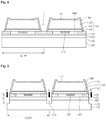
- Fig. 1 is a side-sectional view of a light emitting device according to an embodiment.
- a light emitting device 100 may include a conductive support member 170 having a stepped portion 172 on a side surface thereof, a junction layer 160 on the conductive support member 170, a reflective layer 150 on the junction layer 160, a channel layer 130 around a top surface of the reflective layer 150, an ohmic layer 140 on the reflective layer 150, a light emitting structure 110 disposed on the ohmic layer 140 and the channel layer 130 to generate light, a first passivation layer 180 on a side surface of the light emitting structure 110, a second passivation layer 190 on side surfaces of the light emitting structure 110 and the conductive support member 170, and an electrode 175 on the light emitting structure 110.
- the conductive support member 170 may support the light emitting structure 110. Also, the conductive support member 170 together with the electrode 175 may provide a power to the light emitting device 100.
- the conductive support member 170 may be formed of at least one of Cu, Au, Ni, Mo, Cu-W, and a carrier wafer (e.g., Si, Ge, GaAs, ZnO, SiC, SiGe, or etc,).
- the conductive support member 170 may have a sufficient thickness, for example, a thickness of about 50 ⁇ m to about 500 ⁇ m to support the light emitting structure 110.
- the stepped portion 172 is disposed on a side surface of the conductive support member 170. Since the stepped portion 172 is provided, damage of the light emitting structure 110 by energy of a laser used in a laser scribing process through which a plurality of light emitting devices is separated into individual device units may be minimized.
- the stepped portion 172 is spaced from a bottom surface of the light emitting structure 110 by a first distance h having a height of about 60 ⁇ m to about 120 ⁇ m. That is, since the laser energy is concentrated onto a top surface of the stepped portion 172 in the laser scribing process, an impact by the laser may be transferred onto the light emitting structure 110 spaced the first distance h from the stepped portion 172. This may be described in detail in a method for fabricating the light emitting device according to an embodiment.
- the junction layer 160 may be disposed on the conductive support member 170.
- the junction layer 160 may be disposed to improve an adhesion of an interface between the conductive support member 170 and the reflective layer 150.
- the conductive support member 170 is described as an example in the embodiment, the present disclosure is not limited to the conductive support member.
- a non-conductive support member may be applicable.
- a through-hole for electrical connection may be defined inside or outside the support member.
- a vertical type chip structure is described as an example, the present disclosure is not limited thereto.
- a lateral type chip or a flip type chip may be applicable.
- the junction layer 160 may be formed of a metal material having superior adhesion, for example, at least one of Ti, Au, Sn, Ni, Cr, Ga, In, Bi, Cu, Ag, and Ta.
- the junction layer 160 may have a single- or multi-layered structure. However, when the conductive support member 170 is formed using a plating or deposition process, but a bonding process, the junction layer 160 may not be provided.
- the reflective layer 150 may be disposed on the junction layer 160.
- the reflective layer 150 may reflect light incident from the light emitting structure 110 to improve light efficiency of the light emitting device 100.
- the reflective layer 150 may be formed of a metal material having high reflectance, for example, at least one metal of Ag, Al, Pd, Cu, and Pt, or alloys thereof.
- the channel layer 130 is disposed in a circumference region of a top surface of the reflective layer 150, i.e., a circumference region between the reflective layer 150 and the light emitting structure 110.
- the channel layer 130 may prevent the light emitting structure 110 and the conductive support member 170 from being electrically short-circuited to each other and prevent moisture from being permeated between the light emitting structure 110 and the conductive support member 170.
- the channel layer 130 may be formed of oxide or nitride, for example, at least one of Si0 2 , Si x O y , Si 3 N 4 , Si x N y , SiO x N y , Al 2 O 3 , TiO 2 , ITO, AZO, and ZnO.
- the ohmic layer 140 may be disposed on the reflective layer 150.
- the ohmic layer 140 may be disposed to realize ohmic-contact between the reflective layer 150 and the light emitting structure 110.
- the ohmic layer 140 may selectively use a light-transmitting conductive layer and a metal.
- the ohmic layer 140 may have a single- or multi-layered structure.
- the ohmic layer 140 may be formed of at least one of indium tin oxide (ITO), indium zinc oxide (IZO), indium zinc tin oxide (IZTO), indium aluminum zinc oxide (IAZO), indium gallium zinc oxide (IGZO), indium gallium tin oxide (IGTO), aluminum zinc oxide (AZO), antimony tin oxide (ATO), gallium zinc oxide (GZO), IrO x , RuO x , Ni, Ag, and Au.
- ITO indium tin oxide
- IZO indium zinc oxide
- IZTO indium aluminum zinc oxide
- IGZO indium gallium zinc oxide
- IGTO aluminum zinc oxide
- ATO antimony tin oxide
- GZO gallium zinc oxide
- the ohmic layer 140 may not be provided.
- a current blocking layer 120 is disposed between the ohmic layer 140 and the light emitting structure 110.
- the current blocking layer 120 vertically overlaps the electrode 175.
- the current blocking layer formed of a material having conductivity or insulativity less than that of the reflective layer 150 or the junction layer 160 or a material, which schottky-contacts a second conductive type semiconductor layer 116.
- the current blocking layer 120 may be formed of at least one of ZnO, SiO 2 , SiO x , SiO x N y , Si 3 N 4 , Al 2 O 3 , TiO x , Ti, Al, and Cr.
- the current blocking layer 120 may prevent a current from concentrately flowing into the shortest distance between the conductive support member 170 and the electrode 175 to improve the light efficiency of the light emitting device 100.
- the light emitting structure 110 may be disposed on the ohmic layer 140 and the channel layer 130.
- the light emitting structure 110 may include a plurality of compound semiconductor layers.
- the light emitting structure 110 may include a second conductive type semiconductor layer 116, an active layer 114 on the second conductive type semiconductor layer 116, and a first conductive type semiconductor layer 112 on the active layer 114.
- the second conductive type semiconductor layer 116 may be realized as a P-type semiconductor layer.
- the P-type semiconductor layer may be formed of a semiconductor material having a compositional formula of In x Al y Ga 1-x-y N (0 ⁇ x ⁇ 1, 0 ⁇ y ⁇ 1, 0 ⁇ x+y ⁇ 1), e.g., one of InAlGaN, GaN, AlGaN, AlInN, InGaN, AlN, and InN.
- the P-type semiconductor layer may be doped with a P-type dopant such as Mg, Zn, Ca, Sr, or Ba.
- the active layer 114 may be formed of a semiconductor material having a compositional formula of In x Al y Ga 1-x-y N (0 ⁇ x ⁇ 1, 0 ⁇ y ⁇ 1, 0 ⁇ x+y ⁇ 1). Also, the active layer 114 may have one of a single quantum well structure, a multi quantum well (MQW) structure, a quantum wire structure, and a quantum dot structure.
- MQW multi quantum well
- the active layer 114 may have the quantum well structure
- the active layer 114 may have a single or quantum well structure including a well layer having a compositional formula of In x Al y Ga 1-x-y N (0 ⁇ x ⁇ 1, 0 ⁇ y ⁇ 1, 0 ⁇ x+y ⁇ 1) and a barrier layer having a compositional formula of In a Al b Ga 1-a-b N (0 ⁇ a ⁇ 1, 0 ⁇ b ⁇ 1, 0 ⁇ a+b ⁇ 1).
- the well layer may be formed of a material having an energy band gap less than that of the barrier layer.
- the active layer 114 may generate light using energy generated by recombination of electrons and holes provided from the first conductive type semiconductor layer 112 and the second conductive type semiconductor layer 116.
- the first conductive type semiconductor layer 112 may include an N-type semiconductor layer.
- the N-type semiconductor layer may be formed of a semiconductor material having a compositional formula of In x Al y Ga 1-x-y N (0 ⁇ x ⁇ 1, 0 ⁇ y ⁇ 1, 0 ⁇ x+y ⁇ 1), e.g., one of InAlGaN, GaN, AlGaN, AlInN, InGaN, AlN, and InN.
- the N-type semiconductor layer may be doped with an N-type dopant such as Si, Ge, or Sn.
- a light extraction pattern 111 may be disposed on a top surface of the first conductive type semiconductor layer 112.
- the light extraction pattern 111 may have a random roughness shape or a regular shape.
- the light extraction pattern 111 may have a photonic crystal structure in which light having a specific wavelength band is selectively transmitted or reflected and have a period of about 50 nm to about 3000 nm, but is not limited thereto.
- a conductive type semiconductor layer different from the second conductive type semiconductor layer 116 may be disposed below the second conductive type semiconductor layer 116.
- the first conductive type semiconductor layer 112 may be realized as a P-type semiconductor layer
- the second conductive type semiconductor layer 116 may be realized as an N-type semiconductor layer.
- the light emitting structure 110 may has at least one of an N-P junction structure, a P-N junction structure, an N-P-N junction structure, and a P-N-P junction structure, but is not limited thereto.
- the first passivation layer 180 is disposed on a side surface of the light emitting structure 110.
- the first passivation layer 180 has one end disposed on a top surface of the light emitting structure 110 and the other end disposed on a top surface of the channel layer 130 along the side surface of the light emitting structure 110, but is not limited thereto.
- the second passivation layer 190 is disposed on side surfaces of the light emitting structure 110 and the conductive support member 170. Specifically, the second passivation 190 is disposed outside the first passivation 180, the channel layer 130, the reflective layer 140, the junction layer 150, and the conductive support member 170.
- the second passivation layer 190 has one end 190a disposed on the top surface of the light emitting structure 110 and the other end 190b disposed on the stepped portion 172 of the conductive support member 170 along side surfaces of the light emitting structure 110 and the conductive support member 170, but is not limited thereto.
- the first and second passivation layers 180 and 190 may prevent the light emitting structure 110 from being electrically short-circuited to an external electrode.
- Each of the first and second passivation layers 180 and 190 may be formed of oxide or nitride, e.g., one of SiO 2 , SiO x , SiO x N y , Si 3 N 4 , and Al 2 O 3 , but is not limited thereto.
- the first and second passivation layers 189 and 190 may be formed of the same material as each other, but is not limited thereto.
- the second passivation layer 190 may prevent the light emitting structure 110 and the structures disposed below the reflective layer 150 from being exfoliated from each other.
- the electrode 175 may be disposed on the first conductive type semiconductor layer 112 of the light emitting structure 110.
- the electrode 175 may be formed of at least one of Au, Ti, Cu, Ni, and Cr, and have a single- or multi-layered structure, but is not limited thereto.
- the light extraction pattern 111 on the first conductive type semiconductor layer 112 may be transferred onto a top surface of the electrode 175 to form a roughness 176.
- the electrode 175 is disposed on the top surface of the light emitting structure 110 in the current embodiment, the present disclosure is not limited thereto.
- a hybrid structure formed inside the light emitting structure may be applicable to the electrode.
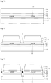
- Figs. 2 to 11 are views illustrating a process for fabricating the light emitting device 100 according to an embodiment.
- a light emitting structure 110 may be formed on a substrate 105.
- the substrate 105 may be formed of at least one of sapphire (Al 2 O 3 ), SiC, GaAs, GaN, ZnO, Si, GaP, InP, Ge, and Ga 2 O 3 , but is not limited thereto.
- a second conductive type semiconductor layer 112, an active layer 114, and a first conductive type semiconductor layer 116 may be sequentially grown on the substrate 105 to form the light emitting structure 110.
- the light emitting structure 110 may be formed using one of a metal organic chemical vapor deposition (MOCVD) process, a chemical vapor deposition (CVD) process, a plasma-enhanced chemical vapor deposition (PECVD) process, a molecular beam epitaxy (MBE) process, and a hydride vapor phase epitaxy (HVPE) process, but is not limited thereto.
- MOCVD metal organic chemical vapor deposition
- CVD chemical vapor deposition
- PECVD plasma-enhanced chemical vapor deposition
- MBE molecular beam epitaxy
- HVPE hydride vapor phase epitaxy
- a buffer layer (not shown) may be further formed between the first conductive type semiconductor layer 112 and the substrate 105 to reduce a lattice constant difference therebetween.
- a channel layer 130 and a current blocking layer 120 are formed on a top surface of the light emitting structure 110.
- the channel layer 130 may be formed in a boundary region of a unit chip (1 chip) using a mask pattern.
- the channel layer 130 may have a ring shape (closed shape), a loop shape, or a frame shape.
- the channel layer 130 may be formed using at least one of an E-beam deposition process, a sputtering process, and a plasma enhanced chemical vapor deposition (PECVD) process.
- PECVD plasma enhanced chemical vapor deposition
- At least one the current blocking layer 120 vertically overlaps the electrode 175 that will be formed later).
- the current blocking layer 120 may be formed using a deposition or plating process.
- an ohmic layer 140 may be formed on the second conductive type semiconductor layer 116, and a reflective layer 150 may be formed on the ohmic layer 140 and the channel layer 130.
- the ohmic layer 140 and the reflective layer 150 may be formed using at least one deposition process of an E-beam deposition process, a sputtering process, and a plasma enhanced chemical vapor deposition (PECVD) process or a plating process, but is not limited thereto.
- PECVD plasma enhanced chemical vapor deposition
- a junction layer 160 may be formed on the reflective layer 150, and a conductive support member 170 may be formed on the junction layer 160.
- the conductive support member 170 may be firmly bonded by the junction layer 160.
- the junction layer 160 may be not formed.
- the substrate 105 may be removed.
- the substrate 105 may be removed by at least one of a laser lift off (LLO) method, a chemical lift off (CLO) method, and a physical polishing method.
- LLO laser lift off
- CLO chemical lift off
- the LLO method is a process in which a laser is irradiated onto the substrate through a back surface of the substrate 105 to exfoliate an interface between the substrate 105 and the first conductive type semiconductor layer 112.
- the CLO method is a process for removing the substrate 105 using an etchant.
- the physical polishing method is a process for physically polishing the substrate 105.
- an under surface of the first conductive type semiconductor layer 112 may be exposed.
- an isolation etching process may be performed on the light emitting structure 110 along a chip boundary region I to separate the light emitting structure 110 of the plurality of light emitting devices into individual light emitting device units.
- a structure in which the light emitting device described in the fabrication process of Fig. 6 turns upside down will be described.
- the isolation etching process may be performed by a dry etch process such as an inductively coupled plasma (ICP) process.
- ICP inductively coupled plasma
- a passivation layer 180 is formed on a side surface of the light emitting structure 110.
- the first passivation layer 180 may be formed using at least one deposition process of an E-beam deposition process, a sputtering process, and a plasma enhanced chemical vapor deposition (PECVD) process or a plating process, but is not limited thereto.
- PECVD plasma enhanced chemical vapor deposition
- a light extraction pattern 111 may be formed on the first conductive type semiconductor layer 112.
- the light extraction pattern 111 may have a random shape by a wet etch process or a photonic crystal structure along a mask pattern, but is not limited thereto.
- the light extraction pattern 111 may be previously formed before the first passivation layer 180 is formed, but is not limited thereto.
- an etch process may be performed between the light emitting structures 110 divided into the individual light emitting device unit.
- a portion of the channel layer 130, the reflective layer 150, the junction layer 160, and the conductive support member 170 may be removed by the etch process to form a groove 173, and a stepped portion 172 is formed on a side surface of the conductive support member 170. That is, the stepped portion 172 may be formed on a circumference region of the light emitting device 100 according to an embodiment along a chip boundary region.
- the top surface of the stepped portion 172 is spaced from a bottom surface of the light emitting structure 110 by a first distance h.
- the first distance h is about 60 ⁇ m to about 120 ⁇ m.
- the etch process may include a wet etch process or a dry etch process, e.g., a dry etch process using inductively couple plasma (ICP).
- ICP inductively couple plasma
- the channel layer 130, the reflective layer 150, the junction layer 160, and the conductive support member 170 may have curved side surfaces.
- an electrode 175 is formed on the first conductive type semiconductor layer 112.
- the electrode 175 may be formed using a plating or deposition process.
- the second passivation layer 190 has one end 190a disposed on a top surface of the light emitting structure 110 and the other end 190b disposed on the stopped portion 172 of the conductive support member 170 along the side surface of the light emitting structure 110, but is not limited thereto.
- a chip separation process using a laser scribing process may be performed along the stepped portion 172 to separate the plurality of light emitting devices into individual light emitting device units, thereby providing the light emitting device 100 according to an embodiment.
- the laser scribing process is a process in which a laser is irradiated along a chip boundary to separate the chip into unit chips.
- the light emitting device 100B may have the same structure as the light emitting device 100 of Fig. 1 except existence and inexistence of the channel layer and the first passivation layer.
- a light emitting device 100B may include a conductive support member 170 having a stepped portion 172 on a side surface thereof, a junction layer 160 on the conductive support member 170, a reflective layer 150 on the junction layer 160, an ohmic layer 140 on the reflective layer 150, a light emitting structure 110 disposed on the ohmic layer 140 to generate light, a passivation layer 190 on side surfaces of the light emitting structure 110 and the conductive support member 170, and an electrode 175 on the light emitting structure 110.
- Figs. 13 to 20 are views illustrating a process for fabricating the light emitting device 100B of Fig. 12 .
- the explanations duplicated with the aforementioned embodiment will be omitted or simply described.
- a light emitting structure 110 may be formed on a substrate 105.
- a first conductive type semiconductor layer 112, an active layer 114, and a second conductive type semiconductor layer 116 may be sequentially grown on the substrate 105 to form the light emitting structure 110.
- At least one of the current blocking layer 120 may vertically overlap an electrode 175 that will be formed later.
- the current blocking layer 120 may be formed using a deposition or plating process.
- an ohmic layer 140 may be formed on the second conductive type semiconductor layer 116 and the current blocking layer 120, a reflective layer 150 may be formed on the ohmic layer 140, and a junction layer 160 may be formed on the reflective layer 150, and a conductive support member 170 may be formed on the junction layer 160.
- the substrate 105 may be removed.
- the substrate 105 may be removed by at least one of a laser lift off (LLO) method, a chemical lift off (CLO) method, and a physical polishing method.
- LLO laser lift off
- CLO chemical lift off
- an isolation etching process may be performed on the light emitting structure 110 along a chip boundary region I to separate the light emitting structure 110 of the plurality of light emitting devices into individual light emitting device units.
- a structure in which the light emitting device described in the fabrication process of Fig. 6 turns upside down will be described.
- an etch process may be performed between the light emitting structures 110 divided into the individual light emitting device unit.
- the second passivation 190 may be formed outside the first passivation layer 180, the channel layer 130, the reflective layer 140, the junction layer 150, and the conductive support member 170.
Description
- Embodiments relate to a light emitting device, a method for fabricating the light emitting device, a light emitting device package, and a lighting unit.
- A light emitting diode (LED) is a kind of a semiconductor device for converting electric energy into light. The LED has advantages such as low power consumption, a semi-permanent life cycle, a fast response time, safety, and environment friendly compared to the related art light source such as a fluorescent lamp and an incandescent bulb. Many studies are being in progress in order to replace the related art light source with an LED. Also, the LED is being increasingly used according to the trend as light sources of a lighting device such as a variety of lamps and streetlights, a lighting unit of a liquid crystal display device, and a scoreboard in indoor and outdoor places.
- The documents
US 2005/017258 A1 ,US 4966862 A , andUS 2007/187702 discloses LED devices comprising a passivation layer formed over the lateral side surfaces of the light emitting structure and over the side surfaces of a stepped portion formed on the substrate. - Document
US 2010/065872 A1 discloses a LED device comprising a channel layer formed under the light emitting structure. - The invention is concerning a LED device and method for
fabrication according claims - Embodiments provide a light emitting device having a new structure, a method for fabricating the light emitting device, a light emitting device package, and a lighting unit.
- Embodiments also provide a light emitting device having improved reliability, a method for fabricating the light emitting device, a light emitting device package, and a lighting unit.
- In one embodiment, a light emitting device includes: a support member having a stepped portion on a side surface; a light emitting structure on the support member, the light emitting structure including a first conductive type semiconductor layer, an active layer, and a second conductive type semiconductor layer to generate light; and an electrode supplying a power to the first conductive type semiconductor layer, wherein the support member has a first surface on which the light emitting structure is disposed and a second surface having an area greater than that of the first surface.
- In another embodiment, a method for fabricating a light emitting device includes: sequentially forming a first conductive type semiconductor layer, an active layer, and a second semiconductor layer to form a light emitting structure; forming a support member on a top surface of the light emitting structure; performing an isolation etching process on the light emitting structure along a chip boundary region to divide the light emitting structure into individual light emitting device units; performing an etch process between the light emitting structures separated into the individual light emitting device units to remove at least portion of the support member; and performing a laser scribing process along the chip boundary region to separate a plurality of light emitting devices into individual light emitting device units.
- In further another embodiment, a light emitting device package includes: a body; first and second electrode layers on the body; and a light emitting device electrically connected the first and second electrode layers to generate light, wherein the light emitting device includes: a support member having a stepped portion on a side surface; a light emitting structure on the support member, the light emitting structure including a first conductive type semiconductor layer, an active layer, and a second conductive type semiconductor layer to generate light; and an electrode supplying a power to the first conductive type semiconductor layer, wherein the support member has a first surface on which the light emitting structure is disposed and a second surface having an area greater than that of the first surface.
- In still further another embodiment, a lighting unit includes: a module substrate; and a plurality of light emitting devices mounted on the module substrate, wherein each of the plurality of light emitting device includes a support member having a stepped portion on a side surface; a light emitting structure on the support member, the light emitting structure including a first conductive type semiconductor layer, an active layer, and a second conductive type semiconductor layer to generate light; and an electrode supplying a power to the first conductive type semiconductor layer, wherein the support member has a first surface on which the light emitting structure is disposed and a second surface having an area greater than that of the first surface.
- The details of one or more embodiments are set forth in the accompanying drawings and the description below. Other features will be apparent from the description and drawings, and from the claims.
-
-
Fig. 1 is a side-sectional view of a light emitting device according to an embodiment forming part of the invention. -
Figs. 2 to 11 are views illustrating a process for fabricating the light emitting device ofFig. 1 . -
Fig. 12 is a side-sectional view of a light emitting device according to another embodiment not forming part of the invention. -
Figs. 13 to 20 are views illustrating a process for fabricating the light emitting device ofFig. 12 . -
Fig. 21 is a side-sectional view of a light emitting device package including a light emitting device according to an embodiment. -
Figs. 22 and23 are views of a lighting unit including a light emitting device according to an embodiment. - In the descriptions of embodiments, it will be understood that when a layer (or film), a region, a pattern, or a structure is referred to as being 'on' a substrate, a layer (or film), a region, a pad, or patterns, it can be directly on another layer or substrate, or intervening layers may also be present. Further, it will be understood that when a layer is referred to as being 'under' another layer, it can be directly under another layer, and one or more intervening layers may also be present. Further, the reference about 'on' and 'under' each layer will be made on the basis of drawings.
- In the drawings, the thickness or size of each layer is exaggerated, omitted, or schematically illustrated for convenience in description and clarity. Also, the size of each element does not entirely reflect an actual size.
- Hereinafter, a light emitting device, a method for fabricating the light emitting device, a light emitting device package, and a lighting unit according to an embodiment will be described with reference to accompanying drawings.
-
Fig. 1 is a side-sectional view of a light emitting device according to an embodiment. - Referring to
Fig. 1 , alight emitting device 100 according to an embodiment may include aconductive support member 170 having astepped portion 172 on a side surface thereof, ajunction layer 160 on theconductive support member 170, areflective layer 150 on thejunction layer 160, achannel layer 130 around a top surface of thereflective layer 150, anohmic layer 140 on thereflective layer 150, alight emitting structure 110 disposed on theohmic layer 140 and thechannel layer 130 to generate light, afirst passivation layer 180 on a side surface of thelight emitting structure 110, asecond passivation layer 190 on side surfaces of thelight emitting structure 110 and theconductive support member 170, and anelectrode 175 on thelight emitting structure 110. - The
conductive support member 170 may support thelight emitting structure 110. Also, theconductive support member 170 together with theelectrode 175 may provide a power to thelight emitting device 100. For example, theconductive support member 170 may be formed of at least one of Cu, Au, Ni, Mo, Cu-W, and a carrier wafer (e.g., Si, Ge, GaAs, ZnO, SiC, SiGe, or etc,). - The
conductive support member 170 may have a sufficient thickness, for example, a thickness of about 50 µm to about 500 µm to support thelight emitting structure 110. - Also, the
stepped portion 172 is disposed on a side surface of theconductive support member 170. Since thestepped portion 172 is provided, damage of thelight emitting structure 110 by energy of a laser used in a laser scribing process through which a plurality of light emitting devices is separated into individual device units may be minimized. - For this, the
stepped portion 172 is spaced from a bottom surface of thelight emitting structure 110 by a first distance h having a height of about 60 µm to about 120 µm. That is, since the laser energy is concentrated onto a top surface of thestepped portion 172 in the laser scribing process, an impact by the laser may be transferred onto thelight emitting structure 110 spaced the first distance h from thestepped portion 172. This may be described in detail in a method for fabricating the light emitting device according to an embodiment. - The
junction layer 160 may be disposed on theconductive support member 170. Thejunction layer 160 may be disposed to improve an adhesion of an interface between theconductive support member 170 and thereflective layer 150. - Although the
conductive support member 170 is described as an example in the embodiment, the present disclosure is not limited to the conductive support member. For example, a non-conductive support member may be applicable. In this case, a through-hole for electrical connection may be defined inside or outside the support member. Also, although a vertical type chip structure is described as an example, the present disclosure is not limited thereto. For example, a lateral type chip or a flip type chip may be applicable. - The
junction layer 160 may be formed of a metal material having superior adhesion, for example, at least one of Ti, Au, Sn, Ni, Cr, Ga, In, Bi, Cu, Ag, and Ta. Thejunction layer 160 may have a single- or multi-layered structure. However, when theconductive support member 170 is formed using a plating or deposition process, but a bonding process, thejunction layer 160 may not be provided. - The
reflective layer 150 may be disposed on thejunction layer 160. Thereflective layer 150 may reflect light incident from thelight emitting structure 110 to improve light efficiency of thelight emitting device 100. - The
reflective layer 150 may be formed of a metal material having high reflectance, for example, at least one metal of Ag, Al, Pd, Cu, and Pt, or alloys thereof. - The
channel layer 130 is disposed in a circumference region of a top surface of thereflective layer 150, i.e., a circumference region between thereflective layer 150 and thelight emitting structure 110. Thechannel layer 130 may prevent thelight emitting structure 110 and theconductive support member 170 from being electrically short-circuited to each other and prevent moisture from being permeated between thelight emitting structure 110 and theconductive support member 170. - The
channel layer 130 may be formed of oxide or nitride, for example, at least one of Si02, SixOy, Si3N4, SixNy, SiOxNy, Al2O3, TiO2, ITO, AZO, and ZnO. - The
channel layer 130 may be formed of a metal material having conductivity and superior adhesion, for example, at least one of Ti, Ni, Pt, Pd, Rh, Ir, and W. In this case, thechannel layer 130 may prevent reliability of thelight emitting device 100 from being deteriorated due to exfoliation of the interface between thelight emitting structure 110 and thereflective layer 150. - The
ohmic layer 140 may be disposed on thereflective layer 150. Theohmic layer 140 may be disposed to realize ohmic-contact between thereflective layer 150 and thelight emitting structure 110. - The
ohmic layer 140 may selectively use a light-transmitting conductive layer and a metal. Theohmic layer 140 may have a single- or multi-layered structure. Theohmic layer 140 may be formed of at least one of indium tin oxide (ITO), indium zinc oxide (IZO), indium zinc tin oxide (IZTO), indium aluminum zinc oxide (IAZO), indium gallium zinc oxide (IGZO), indium gallium tin oxide (IGTO), aluminum zinc oxide (AZO), antimony tin oxide (ATO), gallium zinc oxide (GZO), IrOx, RuOx, Ni, Ag, and Au. - When the
reflective layer 150 ohmic-contacts thelight emitting structure 110, theohmic layer 140 may not be provided. - A
current blocking layer 120 is disposed between theohmic layer 140 and thelight emitting structure 110. - At least portion of the
current blocking layer 120 vertically overlaps theelectrode 175. Also, the current blocking layer formed of a material having conductivity or insulativity less than that of thereflective layer 150 or thejunction layer 160 or a material, which schottky-contacts a second conductivetype semiconductor layer 116. For example, thecurrent blocking layer 120 may be formed of at least one of ZnO, SiO2, SiOx, SiOxNy, Si3N4, Al2O3, TiOx, Ti, Al, and Cr. - The
current blocking layer 120 may prevent a current from concentrately flowing into the shortest distance between theconductive support member 170 and theelectrode 175 to improve the light efficiency of thelight emitting device 100. - The
light emitting structure 110 may be disposed on theohmic layer 140 and thechannel layer 130. - The
light emitting structure 110 may include a plurality of compound semiconductor layers. For example, thelight emitting structure 110 may include a second conductivetype semiconductor layer 116, anactive layer 114 on the second conductivetype semiconductor layer 116, and a first conductivetype semiconductor layer 112 on theactive layer 114. - For example, the second conductive
type semiconductor layer 116 may be realized as a P-type semiconductor layer. The P-type semiconductor layer may be formed of a semiconductor material having a compositional formula of InxAlyGa1-x-yN (0≤x≤1, 0≤y≤1, 0≤x+y≤1), e.g., one of InAlGaN, GaN, AlGaN, AlInN, InGaN, AlN, and InN. The P-type semiconductor layer may be doped with a P-type dopant such as Mg, Zn, Ca, Sr, or Ba. - For example, the
active layer 114 may be formed of a semiconductor material having a compositional formula of InxAlyGa1-x-yN (0≤x≤1, 0≤y≤1, 0≤x+y≤1). Also, theactive layer 114 may have one of a single quantum well structure, a multi quantum well (MQW) structure, a quantum wire structure, and a quantum dot structure. - When the
active layer 114 may have the quantum well structure, theactive layer 114 may have a single or quantum well structure including a well layer having a compositional formula of InxAlyGa1-x-yN (0≤x≤1, 0≤y≤1, 0≤x+y≤1) and a barrier layer having a compositional formula of InaAlbGa1-a-bN (0≤a≤1, 0≤b≤1, 0≤a+b≤1). The well layer may be formed of a material having an energy band gap less than that of the barrier layer. - The
active layer 114 may generate light using energy generated by recombination of electrons and holes provided from the first conductivetype semiconductor layer 112 and the second conductivetype semiconductor layer 116. - For example, the first conductive
type semiconductor layer 112 may include an N-type semiconductor layer. The N-type semiconductor layer may be formed of a semiconductor material having a compositional formula of InxAlyGa1-x-yN (0≤x≤1, 0≤y≤1, 0≤x+y≤1), e.g., one of InAlGaN, GaN, AlGaN, AlInN, InGaN, AlN, and InN. The N-type semiconductor layer may be doped with an N-type dopant such as Si, Ge, or Sn. - A
light extraction pattern 111 may be disposed on a top surface of the first conductivetype semiconductor layer 112. Thelight extraction pattern 111 may have a random roughness shape or a regular shape. - For example, the
light extraction pattern 111 may have a photonic crystal structure in which light having a specific wavelength band is selectively transmitted or reflected and have a period of about 50 nm to about 3000 nm, but is not limited thereto. - A conductive type semiconductor layer different from the second conductive
type semiconductor layer 116 may be disposed below the second conductivetype semiconductor layer 116. Also, the first conductivetype semiconductor layer 112 may be realized as a P-type semiconductor layer, and the second conductivetype semiconductor layer 116 may be realized as an N-type semiconductor layer. Thus, thelight emitting structure 110 may has at least one of an N-P junction structure, a P-N junction structure, an N-P-N junction structure, and a P-N-P junction structure, but is not limited thereto. - The
first passivation layer 180 is disposed on a side surface of thelight emitting structure 110. For example, thefirst passivation layer 180 has one end disposed on a top surface of thelight emitting structure 110 and the other end disposed on a top surface of thechannel layer 130 along the side surface of thelight emitting structure 110, but is not limited thereto. - The
second passivation layer 190 is disposed on side surfaces of thelight emitting structure 110 and theconductive support member 170. Specifically, thesecond passivation 190 is disposed outside thefirst passivation 180, thechannel layer 130, thereflective layer 140, thejunction layer 150, and theconductive support member 170. - The
second passivation layer 190 has oneend 190a disposed on the top surface of thelight emitting structure 110 and theother end 190b disposed on the steppedportion 172 of theconductive support member 170 along side surfaces of thelight emitting structure 110 and theconductive support member 170, but is not limited thereto. - The first and second passivation layers 180 and 190 may prevent the
light emitting structure 110 from being electrically short-circuited to an external electrode. Each of the first and second passivation layers 180 and 190 may be formed of oxide or nitride, e.g., one of SiO2, SiOx, SiOxNy, Si3N4, and Al2O3, but is not limited thereto. Here, the first and second passivation layers 189 and 190 may be formed of the same material as each other, but is not limited thereto. - Also, the
second passivation layer 190 may prevent thelight emitting structure 110 and the structures disposed below thereflective layer 150 from being exfoliated from each other. - The
electrode 175 may be disposed on the first conductivetype semiconductor layer 112 of thelight emitting structure 110. For example, theelectrode 175 may be formed of at least one of Au, Ti, Cu, Ni, and Cr, and have a single- or multi-layered structure, but is not limited thereto. - The
light extraction pattern 111 on the first conductivetype semiconductor layer 112 may be transferred onto a top surface of theelectrode 175 to form aroughness 176. - Although the
electrode 175 is disposed on the top surface of thelight emitting structure 110 in the current embodiment, the present disclosure is not limited thereto. For example, a hybrid structure formed inside the light emitting structure may be applicable to the electrode. - Hereinafter, a method for fabricating the
light emitting device 100 will be described in detail. The explanations duplicated with the aforementioned embodiment will be omitted. -
Figs. 2 to 11 are views illustrating a process for fabricating thelight emitting device 100 according to an embodiment. - Referring to
Fig. 2 , alight emitting structure 110 may be formed on asubstrate 105. - For example, the
substrate 105 may be formed of at least one of sapphire (Al2O3), SiC, GaAs, GaN, ZnO, Si, GaP, InP, Ge, and Ga2O3, but is not limited thereto. - A second conductive
type semiconductor layer 112, anactive layer 114, and a first conductivetype semiconductor layer 116 may be sequentially grown on thesubstrate 105 to form thelight emitting structure 110. - For example, the
light emitting structure 110 may be formed using one of a metal organic chemical vapor deposition (MOCVD) process, a chemical vapor deposition (CVD) process, a plasma-enhanced chemical vapor deposition (PECVD) process, a molecular beam epitaxy (MBE) process, and a hydride vapor phase epitaxy (HVPE) process, but is not limited thereto. - A buffer layer (not shown) may be further formed between the first conductive
type semiconductor layer 112 and thesubstrate 105 to reduce a lattice constant difference therebetween. - Referring to
Fig. 3 , achannel layer 130 and acurrent blocking layer 120 are formed on a top surface of thelight emitting structure 110. - The
channel layer 130 may be formed in a boundary region of a unit chip (1 chip) using a mask pattern. Thechannel layer 130 may have a ring shape (closed shape), a loop shape, or a frame shape. For example, thechannel layer 130 may be formed using at least one of an E-beam deposition process, a sputtering process, and a plasma enhanced chemical vapor deposition (PECVD) process. - At least one the
current blocking layer 120 vertically overlaps theelectrode 175 that will be formed later). Thecurrent blocking layer 120 may be formed using a deposition or plating process. - Referring to
Fig. 4 , anohmic layer 140 may be formed on the second conductivetype semiconductor layer 116, and areflective layer 150 may be formed on theohmic layer 140 and thechannel layer 130. - The
ohmic layer 140 and thereflective layer 150 may be formed using at least one deposition process of an E-beam deposition process, a sputtering process, and a plasma enhanced chemical vapor deposition (PECVD) process or a plating process, but is not limited thereto. - Referring to
Fig. 5 , ajunction layer 160 may be formed on thereflective layer 150, and aconductive support member 170 may be formed on thejunction layer 160. - The
conductive support member 170 may be firmly bonded by thejunction layer 160. When theconductive support member 170 is formed using the deposition or plating process, thejunction layer 160 may be not formed. - Referring to
Figs. 5 and6 , thesubstrate 105 may be removed. Thesubstrate 105 may be removed by at least one of a laser lift off (LLO) method, a chemical lift off (CLO) method, and a physical polishing method. - The LLO method is a process in which a laser is irradiated onto the substrate through a back surface of the
substrate 105 to exfoliate an interface between thesubstrate 105 and the first conductivetype semiconductor layer 112. - The CLO method is a process for removing the
substrate 105 using an etchant. The physical polishing method is a process for physically polishing thesubstrate 105. - As the
substrate 105 is removed, an under surface of the first conductivetype semiconductor layer 112 may be exposed. - Referring to
Fig. 7 , an isolation etching process may be performed on thelight emitting structure 110 along a chip boundary region I to separate thelight emitting structure 110 of the plurality of light emitting devices into individual light emitting device units. However, for convenience of description, a structure in which the light emitting device described in the fabrication process ofFig. 6 turns upside down will be described. - For example, the isolation etching process may be performed by a dry etch process such as an inductively coupled plasma (ICP) process.
- Referring to
Fig. 8 , apassivation layer 180 is formed on a side surface of thelight emitting structure 110. - The
first passivation layer 180 may be formed using at least one deposition process of an E-beam deposition process, a sputtering process, and a plasma enhanced chemical vapor deposition (PECVD) process or a plating process, but is not limited thereto. - After the
first passivation layer 180 is formed, alight extraction pattern 111 may be formed on the first conductivetype semiconductor layer 112. Thelight extraction pattern 111 may have a random shape by a wet etch process or a photonic crystal structure along a mask pattern, but is not limited thereto. - The
light extraction pattern 111 may be previously formed before thefirst passivation layer 180 is formed, but is not limited thereto. - Referring to
Fig. 9 , an etch process may be performed between the light emittingstructures 110 divided into the individual light emitting device unit. - A portion of the
channel layer 130, thereflective layer 150, thejunction layer 160, and theconductive support member 170 may be removed by the etch process to form agroove 173, and a steppedportion 172 is formed on a side surface of theconductive support member 170. That is, the steppedportion 172 may be formed on a circumference region of thelight emitting device 100 according to an embodiment along a chip boundary region. - The top surface of the stepped
portion 172 is spaced from a bottom surface of thelight emitting structure 110 by a first distance h. The first distance h is about 60 µm to about 120 µm. - The etch process may include a wet etch process or a dry etch process, e.g., a dry etch process using inductively couple plasma (ICP).
- When the etch process is performed by the wet etch process that is an isotropic etch process, the
channel layer 130, thereflective layer 150, thejunction layer 160, and theconductive support member 170 may have curved side surfaces. - Referring to
Fig. 10 , anelectrode 175 is formed on the first conductivetype semiconductor layer 112. Theelectrode 175 may be formed using a plating or deposition process. - A
second passivation layer 190 is formed on side surfaces of thelight emitting structure 110 and theconductive support member 170. Specifically, thesecond passivation 190 is formed outside thefirst passivation layer 180, thechannel layer 130, thereflective layer 140, thejunction layer 150, and theconductive support member 170. - The
second passivation layer 190 has oneend 190a disposed on a top surface of thelight emitting structure 110 and theother end 190b disposed on the stoppedportion 172 of theconductive support member 170 along the side surface of thelight emitting structure 110, but is not limited thereto. - Referring to
Figs. 10 and 11 , a chip separation process using a laser scribing process may be performed along the steppedportion 172 to separate the plurality of light emitting devices into individual light emitting device units, thereby providing thelight emitting device 100 according to an embodiment. - The laser scribing process is a process in which a laser is irradiated along a chip boundary to separate the chip into unit chips.
- In the current embodiment, according to the laser scribing process, since the laser is irradiated onto the stepped
portion 172 spaced from thelight emitting structure 110 by the first distance h, damage of thelight emitting structure 110 due to laser energy in the laser scribing process may be minimized. - Also, according to the laser scribing process, the chip separation process may be quickly performed to improve efficiency of the fabrication process.
-
Fig. 12 is a side-sectional view of a light emitting device 100B according to another embodiment. - Referring to
Fig. 12 , the light emitting device 100B may have the same structure as thelight emitting device 100 ofFig. 1 except existence and inexistence of the channel layer and the first passivation layer. - That is, a light emitting device 100B may include a
conductive support member 170 having a steppedportion 172 on a side surface thereof, ajunction layer 160 on theconductive support member 170, areflective layer 150 on thejunction layer 160, anohmic layer 140 on thereflective layer 150, alight emitting structure 110 disposed on theohmic layer 140 to generate light, apassivation layer 190 on side surfaces of thelight emitting structure 110 and theconductive support member 170, and anelectrode 175 on thelight emitting structure 110. - In the light emitting device 100B, a channel layer is not separately manufactured. That is, the
conductive support member 170, thejunction layer 160, thereflective layer 150, and theohmic layer 140 may be selectively removed along a chip boundary region to manufacture the channel layer. -
Figs. 13 to 20 are views illustrating a process for fabricating the light emitting device 100B ofFig. 12 . In descriptions of a fabrication method of the light emitting device 100B, the explanations duplicated with the aforementioned embodiment will be omitted or simply described. - Referring to
Fig. 13 , alight emitting structure 110 may be formed on asubstrate 105. A first conductivetype semiconductor layer 112, anactive layer 114, and a second conductivetype semiconductor layer 116 may be sequentially grown on thesubstrate 105 to form thelight emitting structure 110. - Referring to
Fig. 14 , acurrent blocking layer 120 may be formed on a top surface of thelight emitting structure 110. - At least one of the
current blocking layer 120 may vertically overlap anelectrode 175 that will be formed later. Thecurrent blocking layer 120 may be formed using a deposition or plating process. - Referring to
Fig. 15 , anohmic layer 140 may be formed on the second conductivetype semiconductor layer 116 and thecurrent blocking layer 120, areflective layer 150 may be formed on theohmic layer 140, and ajunction layer 160 may be formed on thereflective layer 150, and aconductive support member 170 may be formed on thejunction layer 160. - Referring to
Figs. 15 and16 , thesubstrate 105 may be removed. Thesubstrate 105 may be removed by at least one of a laser lift off (LLO) method, a chemical lift off (CLO) method, and a physical polishing method. - Referring to
Fig. 17 , an isolation etching process may be performed on thelight emitting structure 110 along a chip boundary region I to separate thelight emitting structure 110 of the plurality of light emitting devices into individual light emitting device units. However, for convenience of description, a structure in which the light emitting device described in the fabrication process ofFig. 6 turns upside down will be described. - Referring to
Fig. 18 , an etch process may be performed between the light emittingstructures 110 divided into the individual light emitting device unit. - A portion of the
channel layer 130, thereflective layer 150, thejunction layer 160, and theconductive support member 170 may be removed by the etch process to form agroove 173, and a steppedportion 172 is formed on a side surface of theconductive support member 170. That is, the steppedportion 172 may be formed on a circumference region of thelight emitting device 100 according to an embodiment along a chip boundary region. - The top surface of the stepped
portion 172 may be spaced from a bottom surface of thelight emitting structure 110 by a first distance h. The first distance h may be about 60 µm to about 120 µm. - The etch process may include a wet etch process or a dry etch process, e.g., a dry etch process using inductively couple plasma (ICP).
- When the etch process is performed by the wet etch process that is an isotropic etch process, the
channel layer 130, thereflective layer 150, thejunction layer 160, and theconductive support member 170 may have curved side surfaces. - Referring to
Fig. 19 , anelectrode 175 may be formed on the first conductivetype semiconductor layer 112. Apassivation layer 190 may be formed on side surfaces of thelight emitting structure 110 and theconductive support member 170. - Specifically, the
second passivation 190 may be formed outside thefirst passivation layer 180, thechannel layer 130, thereflective layer 140, thejunction layer 150, and theconductive support member 170. - The
second passivation layer 190 may have oneend 190a disposed on a top surface of thelight emitting structure 110 and theother end 190b disposed on the stoppedportion 172 of theconductive support member 170 along the side surface of thelight emitting structure 110, but is not limited thereto. - Also, a light extraction structure may be formed on a top surface of the first conductive
type semiconductor layer 112. - Referring to
Fig. 21 , a chip separation process using a laser scribing process may be performed along the steppedportion 172 to separate the plurality of light emitting devices into individual light emitting device units, thereby providing thelight emitting device 100 according to an embodiment. - The laser scribing process is a process in which a laser is irradiated along a chip boundary to separate chips into unit chip.
- In the current embodiment, according to the laser scribing process, since the laser is irradiated onto the stepped
portion 172 spaced from thelight emitting structure 110 by the first distance h, damage of thelight emitting structure 110 due to laser energy in the laser scribing process may be minimized. - Also, according to the laser scribing process, the chip separation process may be quickly performed to improve efficiency of the fabrication process.
-
Fig. 21 is a side-sectional view of a light emitting device package including alight emitting device 100 according to an embodiment. - Referring to
Fig. 21 , a light emitting device package according to an embodiment includes abody 10, first and second electrode layers 31 and 32 disposed on thebody 10, alight emitting device 100 disposed on thebody 10 and electrically connected to the first and second electrode layers 31 and 32, and amolding member 40 surrounding thelight emitting device 100 on thebody 10. - The
body 10 may be formed of a silicon material, a synthetic resin material, or a metal material. An inclined surface may be disposed around thelight emitting device 100. - The
first electrode layer 31 and thesecond electrode layer 32 may be electrically separated from each other and provide a power to thelight emitting device 100. Also, the first and second electrode layers 31 and 32 may reflect light generated in thelight emitting device 100 to improve light efficiency. In addition, the first and second electrode layers 31 and 32 may discharge heat generated in thelight emitting device 100 to the outside. - The
light emitting device 100 may be disposed on thebody 10 or the first orsecond electrode layer - The
light emitting device 100 may be electrically connected to the first and second electrode layers 31 and 32 using one of a wire method, a flip-chip method, and a die bonding method. - The
molding member 40 may surround thelight emitting device 100 to protect thelight emitting device 100. Also, a phosphor may be contained in themolding member 40 to change a wavelength of light emitted from thelight emitting device 100. -
Fig. 22 is view of a backlight unit using a light emitting device according to an embodiment. The backlight unit ofFig. 22 is an example of a lighting unit, but is not limited thereto. - Referring to
Fig. 9 , the backlight unit may include abottom cover 1400, alight guide member 1100 disposed within thebottom cover 1400, and alight emitting module 1000 disposed on at least one surface or an under surface of thelight guide member 1100. Also, areflection sheet 1300 may be disposed below thelight guide member 1100. - The
bottom cover 1400 may have an upwardly opened box shape to receive thelight guide member 1100, thelight emitting module 1000, and thereflection sheet 1300. Also, thebottom cover 1400 may be formed of a metal material or a resin material, but is not limited thereto. - The
light emitting module 1000 may include a substrate and a plurality of light emitting device packages mounted on the substrate. The plurality of light emitting device packages may provide light to thelight guide member 1100. - As shown in
Fig. 9 , thelight emitting module 1000 may be disposed on at least one surface of inner side surfaces of thebottom cover 1400, and thus, thelight emitting module 1000 may provide light toward at least one side surface of thelight guide member 1100. - Alternatively, the
light emitting module 1000 may be disposed on an under surface of thebottom cover 1400 to provide light toward an under surface of thelight guide member 1100. This may be variously varied according to a design of the BLU, but is not limited thereto. - The
light guide member 1100 may be disposed inside thebottom cover 1400. Thelight guide member 1100 may receive the light provided from thelight emitting module 1000 to produce planar light, and then guide the planar light to a liquid crystal panel (not shown). - When the
light emitting module 1000 is disposed on a side surface of thelight guide member 1100, thelight guide member 1100 may be a light guide panel (LGP). - The light guide plate may be formed of one of a resin-based material such as polymethylmethacrylate (PMMA), a polyethylene terephthalate (PET) resin, a poly carbonate (PC) resin, a cyclic olefin copolymer (COC) resin, and a polyethylene naphthalate (PEN) resin.
- When the
light emitting module 100 is disposed on an under surface of thelight guide member 1100, thelight guide member 1100 may include at least one of the light guide panel or an optical sheet. - For example, the optical sheet may include at least one of a diffusion sheet, a light collection sheet, and a brightness enhancement sheet. For example, the diffusion sheet, the light collection sheet, and the brightness enhancement sheet may be stacked to form the optical sheet. In this case, the diffusion sheet 1150 may uniformly diffuse light emitted from the
light emitting module 1000, and the diffused light may be collected into the display panel (not shown) by the light collection sheet. Here, the light emitted from the light collection sheet is randomly polarized light. The bright enhancement sheet may enhance a degree of polarization of the light emitted from the light collection sheet. For example, the light collection sheet may be a horizontal and/or vertical prism sheet. Also, the bright enhancement sheet may be a dual brightness enhancement film. - The
reflective sheet 1300 may be disposed below thelight guide member 1100. Thereflective sheet 1300 may reflects the light emitted through the under surface of thelight guide member 1100 toward a light emitting surface of thelight guide member 1100. - The
reflective sheet 1300 may be formed of a material having superior reflectance, e.g., a PET resin, a PC resin, or a PVC resin, but is not limited thereto. -
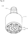
Fig. 23 is a perspective view of alighting unit 1100 including a light emitting device 200 according to an embodiment. However, the lighting unit is an example of a lighting system, and the present disclosure is not limited thereto. - Referring to
Fig. 23 , thelighting unit 1100 may include a case body 1110, alight emitting module 1130 disposed on the case body 1110, aconnection terminal 1120 disposed on the case body 1210 to receive a power from an external power source. - The case body 1110 may be formed of a material having good thermal dissipation properties, e.g., a metal material or a resin material.
- The
light emitting module 1130 may include a substrate 1132 and at least one light emitting device package 200 mounted on the substrate 1132. - A circuit pattern may be printed on a dielectric to form the substrate 1132. For example, the substrate 700 may include a printed circuit board (PCB), a metal core PCB, a flexible PCB, and a ceramic PCB.
- Also, the substrate 1132 may be formed of an effectively reflective material or have a color on which light is effectively reflected from a surface thereof, e.g., a white color or a silver color.
- At least one light emitting device package 200 may be mounted on the substrate 1132. The light emitting device package 200 may include at least one light emitting diode (LED). The LED may include colored LEDs, which respectively emit light having a red color, a green color, a blue color, and a white color and an ultraviolet (UV) LED emitting UV rays.
- The
light emitting module 1130 may have various combinations of the LED to obtain color impression and brightness. For example, the white LED, the red LED, and the green LED may be combined with each other to secure a high color rendering index. - The
connection terminal 1120 may be electrically connected to thelight emitting module 1130 to provide a power to thelight emitting module 1130. Referring toFig. 8 , the connected terminal 1120 is screw-coupled to an external power source in a socket manner, but is not limited thereto. For example, theconnection terminal 1120 may have a pin shape, and thus, be inserted into the external power source. Alternatively, theconnection terminal 1120 may be connected to the external power source by a wire. - The embodiments may provide the light emitting device having a new structure, the method for fabricating the light emitting device, the light emitting device package, and the lighting unit.
- The embodiments may also provide the light emitting device having improved reliability, the method for fabricating the light emitting device, the light emitting device package, and the lighting unit.
- Any reference in this specification to "one embodiment," "an embodiment," "example embodiment," etc., means that a particular feature, structure, or characteristic described in connection with the embodiment is included in at least one embodiment of the invention. The appearances of such phrases in various places in the specification are not necessarily all referring to the same embodiment. Further, when a particular feature, structure, or characteristic is described in connection with any embodiment, it is submitted that it is within the purview of one skilled in the art to effect such feature, structure, or characteristic in connection with other ones of the embodiments.
- Although embodiments have been described with reference to a number of illustrative embodiments thereof, it should be understood that numerous other modifications and embodiments can be devised by those skilled in the art that will fall within the scope of the invention as defined by the appended claims.
Claims (15)
- A light emitting device comprising:a support member (170) having a stepped portion (172) on a side surface;a light emitting structure (110) on the support member (170), the light emitting structure (110) comprising a first conductive type semiconductor layer (112), an active layer (114), and a second conductive type semiconductor layer (116) to generate light;an electrode (175) supplying a power to the first conductive type semiconductor layer (112),wherein the support member (170) has a first surface on which the light emitting structure (110) is disposed and a second surface having an area greater than that of the first surface,characterized in that it further comprisesa channel layer (130) between the light emitting structure (110) and the support member (170), the channel layer (130) being disposed along a circumference of a bottom surface of the light emitting structure (110),a current blocking layer (120) between the light emitting structure (110) and the support member (170), a portion of the current blocking layer (120) vertically overlapping with the electrode (175),a first passivation layer (180) extending from a top surface of the light emitting structure (110) up to a top surface of the channel layer (130),a second passivation layer (190) disposed on the first passivation layer (180), and having one end disposed on the light emitting structure (110) and the other end disposed on the stepped portion (172) along the side surface of the light emitting structure (110) and the support member (170), anda top surface of the stepped portion (172) being spaced from a bottom surface of the light emitting structure (110) by a distance of 60 µm to 120 µm.
- The light emitting device of claim 1, further comprising a reflective layer (150) under the light emitting structure (110), and
a junction layer (160) between the reflective layer (150) and the support member (170),
wherein the support member (170) includes a metal and has a thickness of 50 µm to 500 µm. - The light emitting device of claim 1 or claim 2, wherein the top surface of the channel layer (130) directly contacts a bottom surface of the first passivation layer (180), and
wherein a side surface of the channel layer (130) directly contacts a side surface of the second passivation layer (190). - The light emitting device of any one of claims 1 to 3, wherein each of the first and second passivation layers (180, 190) is formed of at least one selected from the group consisting of SiO2, SiOx, SiOxNy, Si3N4, and Al2O3.
- The light emitting device of any one of claims 1 to 4, wherein the channel layer (130) is formed of at least one selected from the group consisting of Si02, SixOy, Si3N4, SixNy, SiOxNy, Al2O3, TiO2, ITO, AZO, and ZnO.
- The light emitting device of any one of claims 1 to 4, wherein the channel layer (160) is formed of at least one selected from the group consisting of Ti, Ni, Pt, Pd, Rh, Ir, and W.
- The light emitting device of any one of claims 1 to 6, further comprising an ohmic layer (140) between the light emitting structure (110) and the support member (170).
- The light emitting device of claim 2, wherein the channel layer (130) is disposed in a circumference region of a top surface of the reflective layer (150).
- The light emitting device of any one of claims 1 to 8, wherein the first and second passivation layers (180, 190) are formed of the same material as each other.
- The light emitting device of any one of claims 1 to 8, wherein the light emitting structure (110) has a light extraction pattern (111).
- The light emitting device of claim 10, wherein the light extraction pattern (111) includes a roughness disposed on a top surface of first conductive type semiconductor layer (112) of the light emitting structure (110).
- A light emitting device package comprising:a body;first and second electrode layers on the body; anda light emitting device of any one of claims 1 to 11, the light emitting device being disposed on the body and electrically connected the first and second electrode layers to generate light.
- A lighting system comprising:a module substrate; anda light emitting device of any one of claims 1 to 11, the light emitting device being mounted on the module substrate.
- A method for fabricating a light emitting device, the method comprising:sequentially forming a first conductive type semiconductor layer (112), an active layer (114), and a second conductive type semiconductor layer (116) to form a light emitting structure (110);forming a channel layer (130) and a current blocking layer (120) on the light emitting structure (110) ;forming a support member (170) on a top surface of the light emitting structure (110), the channel layer (130) being disposed between the light emitting structure (110) and the support member (170), along a circumference of a bottom surface of the light emitting structure (110);performing an isolation etching process on the light emitting structure (110) along a chip boundary region to divide the light emitting structure (110) into individual light emitting device units;forming a first passivation layer (180) extending from a top surface of the light emitting structure (110) up to a top surface of the channel layer (130);performing an etch process between the light emitting structures (110) separated into the individual light emitting device units to remove at least portion of the support member (170) ;forming a second passivation layer (190) disposed on the first passivation layer (180), and having one end disposed on the light emitting structure (110) and the other end disposed on the stepped portion (172) along the side surface of the light emitting structure (110) and the support member (170);a top surface of the stepped portion (172) being spaced from a bottom surface of the light emitting structure (110) by a distance of 60 µm to 120 µm; andperforming a laser scribing process along the chip boundary region to separate a plurality of light emitting devices into individual light emitting device units.
- The method of claim 14, wherein a top surface of the channel layer (130) is exposed through the isolating etching process on the light emitting structure (110), and
wherein the channel layer serves as an etching stopper.
Applications Claiming Priority (1)
| Application Number | Priority Date | Filing Date | Title |
|---|---|---|---|
| KR20100048597A KR101028277B1 (en) | 2010-05-25 | 2010-05-25 | Light emitting device, method for fabricating the light emitting device, light emitting device package and lighting unit |
Publications (3)
| Publication Number | Publication Date |
|---|---|
| EP2390926A2 EP2390926A2 (en) | 2011-11-30 |
| EP2390926A3 EP2390926A3 (en) | 2015-03-25 |
| EP2390926B1 true EP2390926B1 (en) | 2019-04-03 |
Family
ID=44049907
Family Applications (1)
| Application Number | Title | Priority Date | Filing Date |
|---|---|---|---|
| EP11153925.0A Active EP2390926B1 (en) | 2010-05-25 | 2011-02-09 | Light emitting device, method for fabricating the light emitting device, light emitting device package, and lighting unit |
Country Status (4)
| Country | Link |
|---|---|
| US (1) | US9048377B2 (en) |
| EP (1) | EP2390926B1 (en) |
| KR (1) | KR101028277B1 (en) |
| CN (1) | CN102263182A (en) |
Families Citing this family (41)
| Publication number | Priority date | Publication date | Assignee | Title |
|---|---|---|---|---|
| TW383910U (en) * | 1997-12-17 | 2000-03-01 | Primax Electronics Ltd | Structure of electrode lead plate for double-side & multiple slots socket |
| KR20090115906A (en) * | 2008-05-05 | 2009-11-10 | 송준오 | Methods of surface texture for group 3-nitride semiconductor light emitting diode |
| KR100969100B1 (en) | 2010-02-12 | 2010-07-09 | 엘지이노텍 주식회사 | Light emitting device, method for fabricating the same and light emitting device package |
| EP2555259B1 (en) * | 2010-03-31 | 2018-10-03 | Nichia Corporation | Semiconductor light emitting element |
| EP2528114A3 (en) * | 2011-05-23 | 2014-07-09 | LG Innotek Co., Ltd. | Light emitting device, light emitting device package, and light unit |
| KR101813491B1 (en) | 2011-06-24 | 2017-12-29 | 엘지이노텍 주식회사 | Light emitting device |
| US8426227B1 (en) | 2011-11-18 | 2013-04-23 | LuxVue Technology Corporation | Method of forming a micro light emitting diode array |
| US8573469B2 (en) | 2011-11-18 | 2013-11-05 | LuxVue Technology Corporation | Method of forming a micro LED structure and array of micro LED structures with an electrically insulating layer |
| US8349116B1 (en) | 2011-11-18 | 2013-01-08 | LuxVue Technology Corporation | Micro device transfer head heater assembly and method of transferring a micro device |
| US8333860B1 (en) | 2011-11-18 | 2012-12-18 | LuxVue Technology Corporation | Method of transferring a micro device |
| TWI458122B (en) * | 2011-11-23 | 2014-10-21 | Toshiba Kk | Semiconductor light emitting device |
| US9773750B2 (en) | 2012-02-09 | 2017-09-26 | Apple Inc. | Method of transferring and bonding an array of micro devices |
| US9548332B2 (en) * | 2012-04-27 | 2017-01-17 | Apple Inc. | Method of forming a micro LED device with self-aligned metallization stack |
| US9162880B2 (en) | 2012-09-07 | 2015-10-20 | LuxVue Technology Corporation | Mass transfer tool |
| KR20140044103A (en) * | 2012-10-04 | 2014-04-14 | 삼성디스플레이 주식회사 | Organic light emitting diode display and method for manufacturing the same |
| WO2014201187A2 (en) | 2013-06-12 | 2014-12-18 | Rohinni, Inc. | Keyboard backlighting with deposited light-generating sources |
| US9087764B2 (en) | 2013-07-26 | 2015-07-21 | LuxVue Technology Corporation | Adhesive wafer bonding with controlled thickness variation |
| US9153548B2 (en) | 2013-09-16 | 2015-10-06 | Lux Vue Technology Corporation | Adhesive wafer bonding with sacrificial spacers for controlled thickness variation |
| JP2015082612A (en) * | 2013-10-23 | 2015-04-27 | 旭化成株式会社 | Nitride light-emitting element and method of manufacturing the same |
| US9367094B2 (en) | 2013-12-17 | 2016-06-14 | Apple Inc. | Display module and system applications |
| US9768345B2 (en) | 2013-12-20 | 2017-09-19 | Apple Inc. | LED with current injection confinement trench |
| US9450147B2 (en) | 2013-12-27 | 2016-09-20 | Apple Inc. | LED with internally confined current injection area |
| US9583466B2 (en) | 2013-12-27 | 2017-02-28 | Apple Inc. | Etch removal of current distribution layer for LED current confinement |
| KR102170213B1 (en) * | 2014-01-21 | 2020-10-26 | 엘지이노텍 주식회사 | Light emitting device |
| US9542638B2 (en) | 2014-02-18 | 2017-01-10 | Apple Inc. | RFID tag and micro chip integration design |
| US9583533B2 (en) | 2014-03-13 | 2017-02-28 | Apple Inc. | LED device with embedded nanowire LEDs |
| US9522468B2 (en) | 2014-05-08 | 2016-12-20 | Apple Inc. | Mass transfer tool manipulator assembly with remote center of compliance |
| US9318475B2 (en) | 2014-05-15 | 2016-04-19 | LuxVue Technology Corporation | Flexible display and method of formation with sacrificial release layer |
| US9741286B2 (en) | 2014-06-03 | 2017-08-22 | Apple Inc. | Interactive display panel with emitting and sensing diodes |
| US9624100B2 (en) | 2014-06-12 | 2017-04-18 | Apple Inc. | Micro pick up array pivot mount with integrated strain sensing elements |
| US9570002B2 (en) | 2014-06-17 | 2017-02-14 | Apple Inc. | Interactive display panel with IR diodes |
| US9425151B2 (en) | 2014-06-17 | 2016-08-23 | Apple Inc. | Compliant electrostatic transfer head with spring support layer |
| CN104124268A (en) * | 2014-07-21 | 2014-10-29 | 京东方科技集团股份有限公司 | Organic light emitting diode (OLED) display panel and manufacture method thereof |
| CN104112767B (en) * | 2014-07-28 | 2017-09-19 | 京东方科技集团股份有限公司 | Array base palte, organic LED display panel and display device |
| US9705432B2 (en) | 2014-09-30 | 2017-07-11 | Apple Inc. | Micro pick up array pivot mount design for strain amplification |
| US9828244B2 (en) | 2014-09-30 | 2017-11-28 | Apple Inc. | Compliant electrostatic transfer head with defined cavity |
| US9478583B2 (en) | 2014-12-08 | 2016-10-25 | Apple Inc. | Wearable display having an array of LEDs on a conformable silicon substrate |
| KR102329719B1 (en) * | 2015-02-23 | 2021-11-23 | 쑤저우 레킨 세미컨덕터 컴퍼니 리미티드 | Light emitting device and light unit having thereof |
| KR102298484B1 (en) | 2016-01-15 | 2021-09-03 | 로히니, 엘엘씨. | Apparatus and method for backlighting through a cover on the device |
| US10332817B1 (en) * | 2017-12-01 | 2019-06-25 | Cree, Inc. | Semiconductor die with improved ruggedness |
| CN110993750B (en) * | 2019-12-20 | 2021-04-09 | 深圳第三代半导体研究院 | Vertical light emitting diode and manufacturing method thereof |
Family Cites Families (16)
| Publication number | Priority date | Publication date | Assignee | Title |
|---|---|---|---|---|
| US4966862A (en) | 1989-08-28 | 1990-10-30 | Cree Research, Inc. | Method of production of light emitting diodes |
| DE10148227B4 (en) | 2001-09-28 | 2015-03-05 | Osram Opto Semiconductors Gmbh | Radiation-emitting semiconductor chip, method for its production and radiation-emitting component |
| US6995032B2 (en) | 2002-07-19 | 2006-02-07 | Cree, Inc. | Trench cut light emitting diodes and methods of fabricating same |
| TW200428043A (en) | 2003-04-16 | 2004-12-16 | Sumitomo Chemical Co | Polarizer and its manufacturing method |
| KR100667508B1 (en) | 2004-11-08 | 2007-01-10 | 엘지전자 주식회사 | Light emitting device and method for fabricating the same |
| DE102005055293A1 (en) | 2005-08-05 | 2007-02-15 | Osram Opto Semiconductors Gmbh | Method for producing semiconductor chips and thin-film semiconductor chip |
| KR100714638B1 (en) | 2006-02-16 | 2007-05-07 | 삼성전기주식회사 | Facet extraction type led and method for manufacturing the same |
| KR101113878B1 (en) * | 2006-06-23 | 2012-03-09 | 엘지이노텍 주식회사 | Light emitting diode having vertical topology and method of making the same |
| KR100867541B1 (en) | 2006-11-14 | 2008-11-06 | 삼성전기주식회사 | Method of manufacturing vertical light emitting device |
| JP5179068B2 (en) | 2007-02-14 | 2013-04-10 | 昭和電工株式会社 | Method for manufacturing compound semiconductor device |
| KR100872717B1 (en) | 2007-06-22 | 2008-12-05 | 엘지이노텍 주식회사 | Light emitting device and manufacturing method thereof |
| KR101289230B1 (en) * | 2007-07-23 | 2013-07-29 | 엘지이노텍 주식회사 | Light emitting device and method for manufacturing the same |
| KR101294849B1 (en) | 2007-10-23 | 2013-08-08 | 엘지디스플레이 주식회사 | Backlight assemlby |
| KR20090077425A (en) | 2008-01-11 | 2009-07-15 | 엘지이노텍 주식회사 | Nitride light emitting device and method of making the same |
| KR101008268B1 (en) * | 2008-11-10 | 2011-01-13 | 전자부품연구원 | Vertical Light Emitting Diode and manufacturing method of the same |
| KR100992776B1 (en) | 2008-11-14 | 2010-11-05 | 엘지이노텍 주식회사 | Semiconductor light emitting device and fabrication method thereof |
-
2010
- 2010-05-25 KR KR20100048597A patent/KR101028277B1/en active IP Right Grant
- 2010-12-21 US US12/974,331 patent/US9048377B2/en active Active
-
2011
- 2011-02-09 EP EP11153925.0A patent/EP2390926B1/en active Active
- 2011-03-31 CN CN2011100851274A patent/CN102263182A/en active Pending
Non-Patent Citations (1)
| Title |
|---|
| None * |
Also Published As
| Publication number | Publication date |
|---|---|
| KR101028277B1 (en) | 2011-04-11 |
| EP2390926A2 (en) | 2011-11-30 |
| US20110291134A1 (en) | 2011-12-01 |
| US9048377B2 (en) | 2015-06-02 |
| CN102263182A (en) | 2011-11-30 |
| EP2390926A3 (en) | 2015-03-25 |
Similar Documents
| Publication | Publication Date | Title |
|---|---|---|
| EP2390926B1 (en) | Light emitting device, method for fabricating the light emitting device, light emitting device package, and lighting unit | |
| EP2434545B1 (en) | Light emitting device | |
| EP2445019B1 (en) | Electrode configuration for a light emitting diode | |
| EP2383802B1 (en) | Light emitting device, method of manufacturing the light emitting device, light emitting device package | |
| EP2423987B1 (en) | Light emitting diode, light emitting diode package and light unit having the same | |
| EP2372790B1 (en) | Light emitting diode, light emitting diode package, and lighting system | |
| US8987753B2 (en) | Light emitting device and light emitting device package | |
| KR101734550B1 (en) | Light emitting device and light emitting device package | |
| EP2390934A2 (en) | Light emitting device and light emitting device package | |
| US8173469B2 (en) | Fabrication method of light emitting device | |
| EP2750205B1 (en) | Light emitting device | |
| KR20110118333A (en) | Light emitting device, method for fabricating the light emitting device, light emitting device package and lighting system | |
| KR20120045635A (en) | Light emitting device, method for fabricating the light emitting device, light emitting device package and lighting system | |
| KR101664501B1 (en) | Light emitting device, method for fabricating the light emitting device, light emitting device package and lighting system | |
| KR101786073B1 (en) | Light emitting device, method for fabricating the light emitting device, light emitting device package and lighting system | |
| KR20120029868A (en) | Light emitting device, light emitting device package and lighting system | |
| KR20120022091A (en) | Light emitting device, method for fabricating the light emitting device, light emitting device package and lighting system | |
| KR20120011163A (en) | Light emitting device, method for fabricating the light emitting device, light emitting device package and lighting system | |
| KR20120039411A (en) | Light emitting device, method for fabricating the light emitting device, light emitting device package and lighting system | |
| KR20120088046A (en) | Light emitting device, method for fabricating the light emitting device, light emitting device package and lighting system |
Legal Events
| Date | Code | Title | Description |
|---|---|---|---|
| AK | Designated contracting states |
Kind code of ref document: A2 Designated state(s): AL AT BE BG CH CY CZ DE DK EE ES FI FR GB GR HR HU IE IS IT LI LT LU LV MC MK MT NL NO PL PT RO RS SE SI SK SM TR |
|
| AX | Request for extension of the european patent |
Extension state: BA ME |
|
| PUAI | Public reference made under article 153(3) epc to a published international application that has entered the european phase |
Free format text: ORIGINAL CODE: 0009012 |
|
| 17P | Request for examination filed |
Effective date: 20140328 |
|
| RBV | Designated contracting states (corrected) |
Designated state(s): AL AT BE BG CH CY CZ DE DK EE ES FI FR GB GR HR HU IE IS IT LI LT LU LV MC MK MT NL NO PL PT RO RS SE SI SK SM TR |
|
| RAP1 | Party data changed (applicant data changed or rights of an application transferred) |
Owner name: LG INNOTEK CO., LTD. |
|
| PUAL | Search report despatched |
Free format text: ORIGINAL CODE: 0009013 |
|
| AK | Designated contracting states |
Kind code of ref document: A3 Designated state(s): AL AT BE BG CH CY CZ DE DK EE ES FI FR GB GR HR HU IE IS IT LI LT LU LV MC MK MT NL NO PL PT RO RS SE SI SK SM TR |
|
| AX | Request for extension of the european patent |
Extension state: BA ME |
|
| RIC1 | Information provided on ipc code assigned before grant |
Ipc: H01L 33/00 20100101AFI20150218BHEP Ipc: H01L 33/38 20100101ALN20150218BHEP Ipc: H01L 33/22 20100101ALN20150218BHEP Ipc: H01L 33/44 20100101ALN20150218BHEP Ipc: H01L 33/20 20100101ALI20150218BHEP |
|
| RAP1 | Party data changed (applicant data changed or rights of an application transferred) |
Owner name: LG INNOTEK CO., LTD. |
|
| RIC1 | Information provided on ipc code assigned before grant |
Ipc: H01L 33/44 20100101ALI20180726BHEP Ipc: H01L 33/38 20100101ALN20180726BHEP Ipc: H01L 33/22 20100101ALN20180726BHEP Ipc: H01L 33/20 20100101ALI20180726BHEP Ipc: H01L 33/00 20100101AFI20180726BHEP |
|
| GRAP | Despatch of communication of intention to grant a patent |
Free format text: ORIGINAL CODE: EPIDOSNIGR1 |
|
| STAA | Information on the status of an ep patent application or granted ep patent |
Free format text: STATUS: GRANT OF PATENT IS INTENDED |
|
| RIC1 | Information provided on ipc code assigned before grant |
Ipc: H01L 33/38 20100101ALN20181004BHEP Ipc: H01L 33/00 20100101AFI20181004BHEP Ipc: H01L 33/20 20100101ALI20181004BHEP Ipc: H01L 33/44 20100101ALI20181004BHEP Ipc: H01L 33/22 20100101ALN20181004BHEP |
|
| INTG | Intention to grant announced |
Effective date: 20181015 |
|
| GRAS | Grant fee paid |
Free format text: ORIGINAL CODE: EPIDOSNIGR3 |
|
| GRAA | (expected) grant |
Free format text: ORIGINAL CODE: 0009210 |
|
| STAA | Information on the status of an ep patent application or granted ep patent |
Free format text: STATUS: THE PATENT HAS BEEN GRANTED |
|
| AK | Designated contracting states |
Kind code of ref document: B1 Designated state(s): AL AT BE BG CH CY CZ DE DK EE ES FI FR GB GR HR HU IE IS IT LI LT LU LV MC MK MT NL NO PL PT RO RS SE SI SK SM TR |
|
| REG | Reference to a national code |
Ref country code: GB Ref legal event code: FG4D |
|
| REG | Reference to a national code |
Ref country code: CH Ref legal event code: EP Ref country code: AT Ref legal event code: REF Ref document number: 1116795 Country of ref document: AT Kind code of ref document: T Effective date: 20190415 |
|
| REG | Reference to a national code |
Ref country code: DE Ref legal event code: R096 Ref document number: 602011057684 Country of ref document: DE |
|
| REG | Reference to a national code |
Ref country code: IE Ref legal event code: FG4D |
|
| REG | Reference to a national code |
Ref country code: NL Ref legal event code: MP Effective date: 20190403 |
|
| REG | Reference to a national code |
Ref country code: LT Ref legal event code: MG4D |
|
| REG | Reference to a national code |
Ref country code: AT Ref legal event code: MK05 Ref document number: 1116795 Country of ref document: AT Kind code of ref document: T Effective date: 20190403 |
|
| PG25 | Lapsed in a contracting state [announced via postgrant information from national office to epo] |
Ref country code: NL Free format text: LAPSE BECAUSE OF FAILURE TO SUBMIT A TRANSLATION OF THE DESCRIPTION OR TO PAY THE FEE WITHIN THE PRESCRIBED TIME-LIMIT Effective date: 20190403 |
|
| PG25 | Lapsed in a contracting state [announced via postgrant information from national office to epo] |
Ref country code: NO Free format text: LAPSE BECAUSE OF FAILURE TO SUBMIT A TRANSLATION OF THE DESCRIPTION OR TO PAY THE FEE WITHIN THE PRESCRIBED TIME-LIMIT Effective date: 20190703 Ref country code: HR Free format text: LAPSE BECAUSE OF FAILURE TO SUBMIT A TRANSLATION OF THE DESCRIPTION OR TO PAY THE FEE WITHIN THE PRESCRIBED TIME-LIMIT Effective date: 20190403 Ref country code: SE Free format text: LAPSE BECAUSE OF FAILURE TO SUBMIT A TRANSLATION OF THE DESCRIPTION OR TO PAY THE FEE WITHIN THE PRESCRIBED TIME-LIMIT Effective date: 20190403 Ref country code: FI Free format text: LAPSE BECAUSE OF FAILURE TO SUBMIT A TRANSLATION OF THE DESCRIPTION OR TO PAY THE FEE WITHIN THE PRESCRIBED TIME-LIMIT Effective date: 20190403 Ref country code: PT Free format text: LAPSE BECAUSE OF FAILURE TO SUBMIT A TRANSLATION OF THE DESCRIPTION OR TO PAY THE FEE WITHIN THE PRESCRIBED TIME-LIMIT Effective date: 20190803 Ref country code: AL Free format text: LAPSE BECAUSE OF FAILURE TO SUBMIT A TRANSLATION OF THE DESCRIPTION OR TO PAY THE FEE WITHIN THE PRESCRIBED TIME-LIMIT Effective date: 20190403 Ref country code: CZ Free format text: LAPSE BECAUSE OF FAILURE TO SUBMIT A TRANSLATION OF THE DESCRIPTION OR TO PAY THE FEE WITHIN THE PRESCRIBED TIME-LIMIT Effective date: 20190403 Ref country code: LT Free format text: LAPSE BECAUSE OF FAILURE TO SUBMIT A TRANSLATION OF THE DESCRIPTION OR TO PAY THE FEE WITHIN THE PRESCRIBED TIME-LIMIT Effective date: 20190403 Ref country code: ES Free format text: LAPSE BECAUSE OF FAILURE TO SUBMIT A TRANSLATION OF THE DESCRIPTION OR TO PAY THE FEE WITHIN THE PRESCRIBED TIME-LIMIT Effective date: 20190403 |
|
| PG25 | Lapsed in a contracting state [announced via postgrant information from national office to epo] |
Ref country code: BG Free format text: LAPSE BECAUSE OF FAILURE TO SUBMIT A TRANSLATION OF THE DESCRIPTION OR TO PAY THE FEE WITHIN THE PRESCRIBED TIME-LIMIT Effective date: 20190703 Ref country code: PL Free format text: LAPSE BECAUSE OF FAILURE TO SUBMIT A TRANSLATION OF THE DESCRIPTION OR TO PAY THE FEE WITHIN THE PRESCRIBED TIME-LIMIT Effective date: 20190403 Ref country code: RS Free format text: LAPSE BECAUSE OF FAILURE TO SUBMIT A TRANSLATION OF THE DESCRIPTION OR TO PAY THE FEE WITHIN THE PRESCRIBED TIME-LIMIT Effective date: 20190403 Ref country code: GR Free format text: LAPSE BECAUSE OF FAILURE TO SUBMIT A TRANSLATION OF THE DESCRIPTION OR TO PAY THE FEE WITHIN THE PRESCRIBED TIME-LIMIT Effective date: 20190704 Ref country code: LV Free format text: LAPSE BECAUSE OF FAILURE TO SUBMIT A TRANSLATION OF THE DESCRIPTION OR TO PAY THE FEE WITHIN THE PRESCRIBED TIME-LIMIT Effective date: 20190403 |
|
| PG25 | Lapsed in a contracting state [announced via postgrant information from national office to epo] |
Ref country code: AT Free format text: LAPSE BECAUSE OF FAILURE TO SUBMIT A TRANSLATION OF THE DESCRIPTION OR TO PAY THE FEE WITHIN THE PRESCRIBED TIME-LIMIT Effective date: 20190403 Ref country code: IS Free format text: LAPSE BECAUSE OF FAILURE TO SUBMIT A TRANSLATION OF THE DESCRIPTION OR TO PAY THE FEE WITHIN THE PRESCRIBED TIME-LIMIT Effective date: 20190803 |
|
| REG | Reference to a national code |
Ref country code: DE Ref legal event code: R097 Ref document number: 602011057684 Country of ref document: DE |
|
| PG25 | Lapsed in a contracting state [announced via postgrant information from national office to epo] |
Ref country code: SK Free format text: LAPSE BECAUSE OF FAILURE TO SUBMIT A TRANSLATION OF THE DESCRIPTION OR TO PAY THE FEE WITHIN THE PRESCRIBED TIME-LIMIT Effective date: 20190403 Ref country code: RO Free format text: LAPSE BECAUSE OF FAILURE TO SUBMIT A TRANSLATION OF THE DESCRIPTION OR TO PAY THE FEE WITHIN THE PRESCRIBED TIME-LIMIT Effective date: 20190403 Ref country code: DK Free format text: LAPSE BECAUSE OF FAILURE TO SUBMIT A TRANSLATION OF THE DESCRIPTION OR TO PAY THE FEE WITHIN THE PRESCRIBED TIME-LIMIT Effective date: 20190403 Ref country code: EE Free format text: LAPSE BECAUSE OF FAILURE TO SUBMIT A TRANSLATION OF THE DESCRIPTION OR TO PAY THE FEE WITHIN THE PRESCRIBED TIME-LIMIT Effective date: 20190403 |
|
| PLBE | No opposition filed within time limit |
Free format text: ORIGINAL CODE: 0009261 |
|
| STAA | Information on the status of an ep patent application or granted ep patent |
Free format text: STATUS: NO OPPOSITION FILED WITHIN TIME LIMIT |
|
| PG25 | Lapsed in a contracting state [announced via postgrant information from national office to epo] |
Ref country code: SM Free format text: LAPSE BECAUSE OF FAILURE TO SUBMIT A TRANSLATION OF THE DESCRIPTION OR TO PAY THE FEE WITHIN THE PRESCRIBED TIME-LIMIT Effective date: 20190403 Ref country code: IT Free format text: LAPSE BECAUSE OF FAILURE TO SUBMIT A TRANSLATION OF THE DESCRIPTION OR TO PAY THE FEE WITHIN THE PRESCRIBED TIME-LIMIT Effective date: 20190403 |
|
| 26N | No opposition filed |
Effective date: 20200106 |
|
| PG25 | Lapsed in a contracting state [announced via postgrant information from national office to epo] |
Ref country code: TR Free format text: LAPSE BECAUSE OF FAILURE TO SUBMIT A TRANSLATION OF THE DESCRIPTION OR TO PAY THE FEE WITHIN THE PRESCRIBED TIME-LIMIT Effective date: 20190403 |
|
| PG25 | Lapsed in a contracting state [announced via postgrant information from national office to epo] |
Ref country code: SI Free format text: LAPSE BECAUSE OF FAILURE TO SUBMIT A TRANSLATION OF THE DESCRIPTION OR TO PAY THE FEE WITHIN THE PRESCRIBED TIME-LIMIT Effective date: 20190403 |
|
| REG | Reference to a national code |
Ref country code: CH Ref legal event code: PL |
|
| GBPC | Gb: european patent ceased through non-payment of renewal fee |
Effective date: 20200209 |
|
| REG | Reference to a national code |
Ref country code: BE Ref legal event code: MM Effective date: 20200229 |
|
| PG25 | Lapsed in a contracting state [announced via postgrant information from national office to epo] |
Ref country code: LU Free format text: LAPSE BECAUSE OF NON-PAYMENT OF DUE FEES Effective date: 20200209 Ref country code: MC Free format text: LAPSE BECAUSE OF FAILURE TO SUBMIT A TRANSLATION OF THE DESCRIPTION OR TO PAY THE FEE WITHIN THE PRESCRIBED TIME-LIMIT Effective date: 20190403 |
|
| PG25 | Lapsed in a contracting state [announced via postgrant information from national office to epo] |
Ref country code: LI Free format text: LAPSE BECAUSE OF NON-PAYMENT OF DUE FEES Effective date: 20200229 Ref country code: CH Free format text: LAPSE BECAUSE OF NON-PAYMENT OF DUE FEES Effective date: 20200229 |
|
| PG25 | Lapsed in a contracting state [announced via postgrant information from national office to epo] |
Ref country code: IE Free format text: LAPSE BECAUSE OF NON-PAYMENT OF DUE FEES Effective date: 20200209 Ref country code: GB Free format text: LAPSE BECAUSE OF NON-PAYMENT OF DUE FEES Effective date: 20200209 |
|
| PG25 | Lapsed in a contracting state [announced via postgrant information from national office to epo] |
Ref country code: BE Free format text: LAPSE BECAUSE OF NON-PAYMENT OF DUE FEES Effective date: 20200229 |
|
| REG | Reference to a national code |
Ref country code: DE Ref legal event code: R081 Ref document number: 602011057684 Country of ref document: DE Owner name: SUZHOU LEKIN SEMICONDUCTOR CO. LTD., TAICANG, CN Free format text: FORMER OWNER: LG INNOTEK CO., LTD., SEOUL, KR |
|
| PG25 | Lapsed in a contracting state [announced via postgrant information from national office to epo] |
Ref country code: MT Free format text: LAPSE BECAUSE OF FAILURE TO SUBMIT A TRANSLATION OF THE DESCRIPTION OR TO PAY THE FEE WITHIN THE PRESCRIBED TIME-LIMIT Effective date: 20190403 Ref country code: CY Free format text: LAPSE BECAUSE OF FAILURE TO SUBMIT A TRANSLATION OF THE DESCRIPTION OR TO PAY THE FEE WITHIN THE PRESCRIBED TIME-LIMIT Effective date: 20190403 |
|
| PG25 | Lapsed in a contracting state [announced via postgrant information from national office to epo] |
Ref country code: MK Free format text: LAPSE BECAUSE OF FAILURE TO SUBMIT A TRANSLATION OF THE DESCRIPTION OR TO PAY THE FEE WITHIN THE PRESCRIBED TIME-LIMIT Effective date: 20190403 |
|
| PGFP | Annual fee paid to national office [announced via postgrant information from national office to epo] |
Ref country code: FR Payment date: 20230110 Year of fee payment: 13 |
|
| PGFP | Annual fee paid to national office [announced via postgrant information from national office to epo] |
Ref country code: DE Payment date: 20230104 Year of fee payment: 13 |