EP2390707A1 - Beam scanning system for sensing biological substances - Google Patents
Beam scanning system for sensing biological substances Download PDFInfo
- Publication number
- EP2390707A1 EP2390707A1 EP10013274A EP10013274A EP2390707A1 EP 2390707 A1 EP2390707 A1 EP 2390707A1 EP 10013274 A EP10013274 A EP 10013274A EP 10013274 A EP10013274 A EP 10013274A EP 2390707 A1 EP2390707 A1 EP 2390707A1
- Authority
- EP
- European Patent Office
- Prior art keywords
- light
- scanning system
- optical device
- beam scanning
- biological substance
- Prior art date
- Legal status (The legal status is an assumption and is not a legal conclusion. Google has not performed a legal analysis and makes no representation as to the accuracy of the status listed.)
- Granted
Links
Images


Classifications
-
- G—PHYSICS
- G02—OPTICS
- G02B—OPTICAL ELEMENTS, SYSTEMS OR APPARATUS
- G02B26/00—Optical devices or arrangements for the control of light using movable or deformable optical elements
- G02B26/08—Optical devices or arrangements for the control of light using movable or deformable optical elements for controlling the direction of light
- G02B26/10—Scanning systems
-
- G—PHYSICS
- G02—OPTICS
- G02B—OPTICAL ELEMENTS, SYSTEMS OR APPARATUS
- G02B6/00—Light guides; Structural details of arrangements comprising light guides and other optical elements, e.g. couplings
- G02B6/10—Light guides; Structural details of arrangements comprising light guides and other optical elements, e.g. couplings of the optical waveguide type
- G02B6/12—Light guides; Structural details of arrangements comprising light guides and other optical elements, e.g. couplings of the optical waveguide type of the integrated circuit kind
- G02B2006/12133—Functions
- G02B2006/1215—Splitter
-
- G—PHYSICS
- G02—OPTICS
- G02B—OPTICAL ELEMENTS, SYSTEMS OR APPARATUS
- G02B6/00—Light guides; Structural details of arrangements comprising light guides and other optical elements, e.g. couplings
- G02B6/10—Light guides; Structural details of arrangements comprising light guides and other optical elements, e.g. couplings of the optical waveguide type
- G02B6/12—Light guides; Structural details of arrangements comprising light guides and other optical elements, e.g. couplings of the optical waveguide type of the integrated circuit kind
- G02B2006/12133—Functions
- G02B2006/12159—Interferometer
Definitions
- the present disclosure generally relates to a beam scanning system, and more particularly to a beam scanning system using an optical phased array for sensing biological substances, such as a cancer cell, a microorganism and the like, in a microfluidic pipe.
- a beam scanning system using a laser light source has been extensively used in various fields, such as laser radars, large area scanning displays, free space optical communications, laser printers, barcode readers and the like.
- Various types of beam scanning systems have been developed, for example, a mechanical beam scanning system, a microelectromechanical systems (MEMs) based beam scanning system, a beam scanning system using an optical phased array, and the like.
- MEMs microelectromechanical systems
- the mechanical beam scanning system may generally use a polygon mirror or a holographic disk, so that excellent performance may be exhibited in terms of light utilization efficiency and scanning range.
- the mechanical beam scanning system may require a highly precise optical device for higher accuracy and a structure thereof may be complex, so that it may be disadvantageous in price competitiveness.
- the mechanical beam scanning system operates mechanically, its scanning speed may be limited to a range of milliseconds.
- the MEMs based beam scanning system may also operate mechanically in the same manner as the mechanical beam scanning system, so that its scanning speed may be limited.
- research using a lithium niobate electrooptic prism deflector has been carried out.
- the lithium niobate electrooptic prism deflector is used in the MEMs based beam scanning system, a relatively high scanning speed of a range of nanoseconds may be achieved.
- the lithium niobate electrooptic prism deflector may require a high driving voltage of over 50OV, which may not be practical.
- the beam scanning system using the optical phased array may be advantageous in terms of a low driving voltage and a high scanning speed.
- a beam scanning system includes a light source configured to generate a supercontinuum light beam; an optical device configured to receive the supercontinuum light beam for guidance thereof to at least two output ports; and a power supply unit configured to supply voltage to one output port of the at least two output ports to change a phase of the light beam from said one output port.
- FIG 1 is a schematic diagram showing beam scanning using an optical phased array. As shown in FIG 1 , when beams are projected from light sources of a phased array on the x-y plane into the ⁇ - ⁇ plane, an interference pattern may appear on the ⁇ - ⁇ plane. This appearance of the interference pattern may be accounted for by the following equation.
- a n represents a light beam intensity emitted from an nth light sources
- ⁇ n represents a phase of the light beam emitted from the nth light source
- ⁇ 0 represents a spot size of the light beam
- ⁇ represents a wavelength of the light beam
- L represents a distance between the x-y plane and the ⁇ - ⁇ plane
- x ⁇ and yn represent a location of the nth light sources on the x-y plane.
- a location of the interference pattern may also be changed on the ⁇ - ⁇ plane.
- beam scanning may be performed by changing the location of the interference pattern in one embodiment.
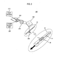
- FIG 2 is a schematic diagram showing an illustrative embodiment of a beam scanning system.
- the beam scanning system 200 may include a light source 210, a power supply unit 220, an optical device 230, a beam focusing unit 240, a mirror 250 and a beam processing unit 260.
- the beam scanning system 200 may further include a storage unit (not shown) for storing information related with a plurality of biological substances ("biological substance related information").
- the biological substance related information may include spectrum data and images, and the like, that are associated with the biological substances.
- the light source 210 may be configured to generate a light beam.
- the light source may include a supercontinuum light source. Any type of light sources capable of generating a supercontinuum light beam may be used as the light source 210.
- the power supply unit 220 may be configured to supply regulated voltages.
- the voltage may be supplied to the optical device 230.
- any types of electric devices capable of supplying regulated voltages may be used as the power supply unit 220.
- the optical device 230 may receive the light beam emitted from the light source 210 for guidance thereof in at least two paths.
- the optical device 230 may be configured to change a phase of the light beam, which passes through one of the paths, responsive to the voltage supplied from the power supply unit 220. Therefore, a location of an interference pattern of the light beam, which is a far-field pattern of the light beam, may be adjusted.
- FIG 3 is a schematic diagram showing an illustrative embodiment of the optical device 230.
- the optical device 230 may include a Y-branch type of optical device.
- the optical device 230 may include an input port 231 and two output ports 232a and 232b.
- the input port 231 may receive the light beam emitted from the light source 210.
- the output port 232a and 232b may branch off from the input port 231.
- the optical device 230 may further include an electrode 233 that may be mounted on one of the output ports 232a and 232b (e.g., output port 232a).
- the voltage may be applied to the electrode 233 such that an electric field is generated.
- a phase of the light beam which is guided by the corresponding output port, e,g., the output port 232a, may be changed in response to the electric field.
- the optical device 230 has two output ports 232a and 232b, the number of the output ports may not be limited thereto.
- the optical device 230 may include more than two output ports.
- the electrode 233 may be mounted on the output port 232a in one embodiment. However, it should be noted herein that the way the electrode 233 is mounted may not be limited thereto.
- the optical device 230 may be mounted on the output port 232b.
- reference numeral "30" represents the interference pattern, which is a far-field pattern of the light beams outputted from the output ports 232a and 232b.
- a carrier density of the light beam which is guided by a waveguide, i.e., the output port 232a, may vary and a refractive index of the light beam may also vary in response to the change of the carrier density.
- the phase of the light beam guided by the output port 232a may be changed, so that a phase difference between the light beams outputted from the output ports 232a and 232b may be caused. If the phase of the supercontinuum light beam is changed as explained above, the position of the interference pattern may also be changed, as shown in equation (1).
- the location of the interference pattern has been adjusted by using the electric field generated by applying the voltage to the electrode 233.
- the adjustment of location of the interference pattern may not be limited thereto.
- an optical field or a microwave may be used to change the phase of the light beam, which may be guided by the optical device, for location adjustment of the interference pattern.
- the beam focusing unit 240 may be configured to focus the light beams outputted from the optical device 230.
- the beam focusing unit 240 may be any devices capable of focusing the light beams, such as a focusing lens.
- the mirror 250 may reflect the light beams, which may be focused in the beam focusing unit 240, to traverse across a target 20, such as a microfluidic pipe.
- the microfluidic pipe 20 may be a pipe in which the biological substances 21 including a cancer cell, a microscopic organism and the like may flow.
- the beam processing unit 260 may be configured to sense the biological substances 21 flowing in the microfluidic pipe 20 based on the light beams, which have traversed across the microfluidic pipe 20. Specially, the beam processing unit 260 may receive the light beams 22 that have traversed across the microfluidic pipe 20 and form biological information on the biological substance based thereon.
- the biological information may include spectrum data and images of the biological substances.
- the beam processing unit 260 may retrieve the biological substance related information from the storage unit and compare the biological information with the retrieved biological substance related information.
- the beam processing unit 260 may form identity information of the biological substance according to the comparison result.
- the identity information may be outputted through an output device (not shown).
- the output device may include a display unit, a printer and the like. Also, the output device may be a storage unit.
- the beam processing unit 260 may include a light sensor array (not shown) in which a plurality of light sensors for sensing different wavelength bands may be arrayed.
- the beam processing unit 260 may include a wide-band light sensor array, in which a plurality light sensors may be included.
- each of the light sensors may have a different wavelength filter.
- the light sensor may include a charge-coupled device for imaging and a spectrometer for spectroscopy. Each of the light sensors may output a sensing signal in response to the received light beam.
- the beam processing unit 260 may successively form an image of the biological substance and sense a spectroscopic peak by combining the sensing signals outputted from the light sensor array.
- an in-situ analysis of the biological substances in the microfluidic pipe may be achieved according to one embodiment.
- the mirror is employed for reflecting the focused light beams to the microfluidic pipe 20.
- the focused light beams may be directly projected to the microfluidic pipe 20.
Landscapes
- Physics & Mathematics (AREA)
- General Physics & Mathematics (AREA)
- Optics & Photonics (AREA)
- Investigating Or Analysing Materials By Optical Means (AREA)
- Investigating Or Analysing Biological Materials (AREA)
- Optical Integrated Circuits (AREA)
- Optical Modulation, Optical Deflection, Nonlinear Optics, Optical Demodulation, Optical Logic Elements (AREA)
Abstract
Description
- The present disclosure generally relates to a beam scanning system, and more particularly to a beam scanning system using an optical phased array for sensing biological substances, such as a cancer cell, a microorganism and the like, in a microfluidic pipe.
- A beam scanning system using a laser light source has been extensively used in various fields, such as laser radars, large area scanning displays, free space optical communications, laser printers, barcode readers and the like. Various types of beam scanning systems have been developed, for example, a mechanical beam scanning system, a microelectromechanical systems (MEMs) based beam scanning system, a beam scanning system using an optical phased array, and the like.
- The mechanical beam scanning system may generally use a polygon mirror or a holographic disk, so that excellent performance may be exhibited in terms of light utilization efficiency and scanning range. However, the mechanical beam scanning system may require a highly precise optical device for higher accuracy and a structure thereof may be complex, so that it may be disadvantageous in price competitiveness. Further, since the mechanical beam scanning system operates mechanically, its scanning speed may be limited to a range of milliseconds.
- The MEMs based beam scanning system may also operate mechanically in the same manner as the mechanical beam scanning system, so that its scanning speed may be limited. In order to resolve the problem of a low scanning speed, research using a lithium niobate electrooptic prism deflector has been carried out. When the lithium niobate electrooptic prism deflector is used in the MEMs based beam scanning system, a relatively high scanning speed of a range of nanoseconds may be achieved. However, the lithium niobate electrooptic prism deflector may require a high driving voltage of over 50OV, which may not be practical.
- Recently, research for a beam scanning system using an optical phased array has been carried out to overcome the above problems. The beam scanning system using the optical phased array may be advantageous in terms of a low driving voltage and a high scanning speed.
- Embodiments for sensing biological substances, such as a cancer cell, a microorganism and the like, in a microfluidic pipe through beam scanning using an optical phased array are disclosed herein. In one embodiment, by way of non-limiting example, a beam scanning system includes a light source configured to generate a supercontinuum light beam; an optical device configured to receive the supercontinuum light beam for guidance thereof to at least two output ports; and a power supply unit configured to supply voltage to one output port of the at least two output ports to change a phase of the light beam from said one output port.
- This Summary is provided to introduce a selection of concepts in a simplified form that are further described below in the Detailed Description. This Summary is not intended to identify key or essential features of the claimed subject matter, nor is it intended to be used in determining the scope of the claimed subject matter.
-
-
FIG. 1 is a schematic diagram showing beam scanning using an optical phased array. -
FIG 2 is a schematic diagram showing an illustrative embodiment of a beam scanning system. -
FIG 3 is a schematic diagram showing an illustrative embodiment of an optical device. - A detailed description may be provided with reference to the accompanying drawings. One of ordinary skill in the art may realize that the following description is illustrative only and is not in any way limiting. Other embodiments of the present invention may readily suggest themselves to such skilled persons having the benefit of this disclosure.
-
FIG 1 is a schematic diagram showing beam scanning using an optical phased array. As shown inFIG 1 , when beams are projected from light sources of a phased array on the x-y plane into the ξ-η plane, an interference pattern may appear on the ξ-η plane. This appearance of the interference pattern may be accounted for by the following equation.
- As shown in equation (1), if a phase of a light beam emitted from the light source is changed, a location of the interference pattern may also be changed on the ξ-η plane. Thus, beam scanning may be performed by changing the location of the interference pattern in one embodiment.
-
FIG 2 is a schematic diagram showing an illustrative embodiment of a beam scanning system. Referring toFIG 2 , thebeam scanning system 200 may include alight source 210, apower supply unit 220, anoptical device 230, abeam focusing unit 240, amirror 250 and abeam processing unit 260. Thebeam scanning system 200 may further include a storage unit (not shown) for storing information related with a plurality of biological substances ("biological substance related information"). The biological substance related information may include spectrum data and images, and the like, that are associated with the biological substances. - The
light source 210 may be configured to generate a light beam. In one embodiment, the light source may include a supercontinuum light source. Any type of light sources capable of generating a supercontinuum light beam may be used as thelight source 210. - The
power supply unit 220 may be configured to supply regulated voltages. The voltage may be supplied to theoptical device 230. In one embodiment, any types of electric devices capable of supplying regulated voltages may be used as thepower supply unit 220. - The
optical device 230 may receive the light beam emitted from thelight source 210 for guidance thereof in at least two paths. Theoptical device 230 may be configured to change a phase of the light beam, which passes through one of the paths, responsive to the voltage supplied from thepower supply unit 220. Therefore, a location of an interference pattern of the light beam, which is a far-field pattern of the light beam, may be adjusted. -
FIG 3 is a schematic diagram showing an illustrative embodiment of theoptical device 230. Referring toFIG 3 , theoptical device 230 may include a Y-branch type of optical device. Theoptical device 230 may include aninput port 231 and twooutput ports input port 231 may receive the light beam emitted from thelight source 210. Theoutput port input port 231. Theoptical device 230 may further include anelectrode 233 that may be mounted on one of theoutput ports output port 232a). The voltage may be applied to theelectrode 233 such that an electric field is generated. Thus, a phase of the light beam, which is guided by the corresponding output port, e,g., theoutput port 232a, may be changed in response to the electric field. - Although the foregoing embodiment has described that the
optical device 230 has twooutput ports optical device 230 may include more than two output ports. Also, theelectrode 233 may be mounted on theoutput port 232a in one embodiment. However, it should be noted herein that the way theelectrode 233 is mounted may not be limited thereto. For example, theoptical device 230 may be mounted on theoutput port 232b. - In
FIG. 3 , reference numeral "30" represents the interference pattern, which is a far-field pattern of the light beams outputted from theoutput ports electrode 233, a carrier density of the light beam, which is guided by a waveguide, i.e., theoutput port 232a, may vary and a refractive index of the light beam may also vary in response to the change of the carrier density. Thus, the phase of the light beam guided by theoutput port 232a may be changed, so that a phase difference between the light beams outputted from theoutput ports - In one embodiment, the location of the interference pattern has been adjusted by using the electric field generated by applying the voltage to the
electrode 233. However, the adjustment of location of the interference pattern may not be limited thereto. In another embodiment, an optical field or a microwave may be used to change the phase of the light beam, which may be guided by the optical device, for location adjustment of the interference pattern. - Referring back to
FIG 2 , thebeam focusing unit 240 may be configured to focus the light beams outputted from theoptical device 230. Thebeam focusing unit 240 may be any devices capable of focusing the light beams, such as a focusing lens. - The
mirror 250 may reflect the light beams, which may be focused in thebeam focusing unit 240, to traverse across atarget 20, such as a microfluidic pipe. Themicrofluidic pipe 20 may be a pipe in which thebiological substances 21 including a cancer cell, a microscopic organism and the like may flow. - The
beam processing unit 260 may be configured to sense thebiological substances 21 flowing in themicrofluidic pipe 20 based on the light beams, which have traversed across themicrofluidic pipe 20. Specially, thebeam processing unit 260 may receive the light beams 22 that have traversed across themicrofluidic pipe 20 and form biological information on the biological substance based thereon. In one embodiment, the biological information may include spectrum data and images of the biological substances. Thebeam processing unit 260 may retrieve the biological substance related information from the storage unit and compare the biological information with the retrieved biological substance related information. Thebeam processing unit 260 may form identity information of the biological substance according to the comparison result. The identity information may be outputted through an output device (not shown). The output device may include a display unit, a printer and the like. Also, the output device may be a storage unit. - In one embodiment, the
beam processing unit 260 may include a light sensor array (not shown) in which a plurality of light sensors for sensing different wavelength bands may be arrayed. In another embodiment, thebeam processing unit 260 may include a wide-band light sensor array, in which a plurality light sensors may be included. In one embodiment, each of the light sensors may have a different wavelength filter. The light sensor may include a charge-coupled device for imaging and a spectrometer for spectroscopy. Each of the light sensors may output a sensing signal in response to the received light beam. Thebeam processing unit 260 may successively form an image of the biological substance and sense a spectroscopic peak by combining the sensing signals outputted from the light sensor array. Thus, an in-situ analysis of the biological substances in the microfluidic pipe may be achieved according to one embodiment. - In the above embodiment, it has been described that the mirror is employed for reflecting the focused light beams to the
microfluidic pipe 20. However, in another embodiment, the focused light beams may be directly projected to themicrofluidic pipe 20. - Although embodiments have been described with reference to a number of illustrative embodiments thereof, it should be understood that numerous other modifications and embodiments can be devised by those skilled in the art that will fall within the scope of the principles of this disclosure. More particularly, numerous variations and modifications are possible in the component parts and/or arrangements of the subject combination arrangement within the scope of the disclosure, the drawings and the appended claims. In addition to variations and modifications in the component parts and/or arrangements, alternative uses will also be apparent to those skilled in the art.
Claims (7)
- A beam scanning system, comprising:a light source configured to generate a supercontinuum light beam;an optical device configured to receive the supercontinuum light beam for guidance thereof to at least two output ports; anda power supply unit configured to supply voltage to one output port of said at least two output ports to change a phase of the light beam from said one output port.
- The beam scanning system of Claim 1, wherein the optical device comprises an input port configured to receive the supercontinuum light beam, and wherein the at least two output ports are configured to branch off from the input port to output the light beam, and the optical device comprises an electrode mounted on said one output port and configured to generate an electric filed responsive to the voltage supplied thereto.
- The beam scanning system of Claim 1 or 2, wherein the optical device further comprises a Y-branch type of optical device.
- The beam scanning system of one of Claims 1 to 3, further comprising:a storage unit to store biological substance related information;a beam focusing unit configured to focus the light beams outputted from the optical device;a mirror configured to reflect the focused beams to traverse across a microfluidic pipe in which a biological substance is allowed to flow; anda beam processing unit configured to receive the light beams that traversed across the microfluidic pipe, said beam processing unit being further configured to form biological information on the biological substance based on the received beams, retrieve the biological substance related information from the storage unit for comparison with the biological information and form identity information of the biological substance flowing in the microfluidic pipe according to the comparison.
- The beam scanning system of Claim 4, wherein the biological information comprises any one of spectrum data and beam image of the biological substance.
- The beam scanning system of Claim 4 or 5, wherein the beam processing unit comprises a light sensor array having a plurality of light sensors each for sensing a different wavelength.
- The beam scanning system of Claim 4 or 6, wherein the beam processing unit comprises a light sensor array having a plurality of light sensors each having a different wavelength filter.
Applications Claiming Priority (1)
| Application Number | Priority Date | Filing Date | Title |
|---|---|---|---|
| KR1020100049185A KR101200536B1 (en) | 2010-05-26 | 2010-05-26 | Beam scanning system for detecting bio-material |
Publications (2)
| Publication Number | Publication Date |
|---|---|
| EP2390707A1 true EP2390707A1 (en) | 2011-11-30 |
| EP2390707B1 EP2390707B1 (en) | 2019-12-04 |
Family
ID=43529988
Family Applications (1)
| Application Number | Title | Priority Date | Filing Date |
|---|---|---|---|
| EP10013274.5A Active EP2390707B1 (en) | 2010-05-26 | 2010-10-04 | Beam scanning system for sensing biological substances |
Country Status (4)
| Country | Link |
|---|---|
| US (1) | US20110292397A1 (en) |
| EP (1) | EP2390707B1 (en) |
| JP (1) | JP5340244B2 (en) |
| KR (1) | KR101200536B1 (en) |
Families Citing this family (2)
| Publication number | Priority date | Publication date | Assignee | Title |
|---|---|---|---|---|
| KR101359708B1 (en) * | 2012-04-04 | 2014-02-10 | 글로벌광통신 (주) | microorganism measurement apparatus |
| JP6765687B2 (en) * | 2016-12-29 | 2020-10-07 | 国立大学法人 東京大学 | Imaging equipment and methods |
Citations (5)
| Publication number | Priority date | Publication date | Assignee | Title |
|---|---|---|---|---|
| EP0729057A2 (en) * | 1995-02-24 | 1996-08-28 | Nippon Telegraph And Telephone Corporation | Coherent white light source and optical devices therewith |
| US20050069258A1 (en) * | 2003-09-29 | 2005-03-31 | Jun-Fei Zheng | Optical waveguide Y-branch splitter |
| US20060237666A1 (en) * | 2005-04-25 | 2006-10-26 | Olympus Corporation | Multiphoton-excitation laser scanning microscope |
| US20080102478A1 (en) * | 2006-09-28 | 2008-05-01 | Washington, University Of | 3d micro-scale engineered tissue model systems |
| US20080180685A1 (en) * | 2007-01-31 | 2008-07-31 | Zygo Corporation | Interferometry for lateral metrology |
Family Cites Families (7)
| Publication number | Priority date | Publication date | Assignee | Title |
|---|---|---|---|---|
| GB8727212D0 (en) * | 1987-11-20 | 1987-12-23 | Secr Defence | Optical beam steering device |
| US5233673A (en) * | 1991-10-09 | 1993-08-03 | Hughes Aircraft Company | Output steerable optical phased array |
| US5608519A (en) * | 1995-03-20 | 1997-03-04 | Gourley; Paul L. | Laser apparatus and method for microscopic and spectroscopic analysis and processing of biological cells |
| JP3730884B2 (en) * | 2000-07-07 | 2006-01-05 | 日本電信電話株式会社 | Optical spectrum flattening method and apparatus |
| US7355716B2 (en) * | 2002-01-24 | 2008-04-08 | The General Hospital Corporation | Apparatus and method for ranging and noise reduction of low coherence interferometry LCI and optical coherence tomography OCT signals by parallel detection of spectral bands |
| US7122384B2 (en) * | 2002-11-06 | 2006-10-17 | E. I. Du Pont De Nemours And Company | Resonant light scattering microparticle methods |
| US20070002336A1 (en) * | 2005-06-30 | 2007-01-04 | Asml Netherlands B.V. | Metrology apparatus, lithographic apparatus, process apparatus, metrology method and device manufacturing method |
-
2010
- 2010-05-26 KR KR1020100049185A patent/KR101200536B1/en not_active Expired - Fee Related
- 2010-09-30 JP JP2010220624A patent/JP5340244B2/en not_active Expired - Fee Related
- 2010-10-01 US US12/896,773 patent/US20110292397A1/en not_active Abandoned
- 2010-10-04 EP EP10013274.5A patent/EP2390707B1/en active Active
Patent Citations (5)
| Publication number | Priority date | Publication date | Assignee | Title |
|---|---|---|---|---|
| EP0729057A2 (en) * | 1995-02-24 | 1996-08-28 | Nippon Telegraph And Telephone Corporation | Coherent white light source and optical devices therewith |
| US20050069258A1 (en) * | 2003-09-29 | 2005-03-31 | Jun-Fei Zheng | Optical waveguide Y-branch splitter |
| US20060237666A1 (en) * | 2005-04-25 | 2006-10-26 | Olympus Corporation | Multiphoton-excitation laser scanning microscope |
| US20080102478A1 (en) * | 2006-09-28 | 2008-05-01 | Washington, University Of | 3d micro-scale engineered tissue model systems |
| US20080180685A1 (en) * | 2007-01-31 | 2008-07-31 | Zygo Corporation | Interferometry for lateral metrology |
Non-Patent Citations (2)
| Title |
|---|
| ANONYMOUS: "Introduction to Integrated Photonics", WILEY, 6 February 2007 (2007-02-06), pages 1 - 23, XP002621363, Retrieved from the Internet <URL:http://media.wiley.com/product_data/excerpt/85/04708486/0470848685.pdf> [retrieved on 20110209] * |
| YIN ET AL: "Ultra-fast speed, low grating lobe optical beam steering using unequally spaced phased array technique", OPTICS COMMUNICATIONS, vol. 270, no. 1, 1 December 2006 (2006-12-01), NORTH-HOLLAND PUBLISHING CO. AMSTERDAM, NL, pages 41 - 46, XP005730457, ISSN: 0030-4018, DOI: 10.1016/J.OPTCOM.2006.11.001 * |
Also Published As
| Publication number | Publication date |
|---|---|
| KR101200536B1 (en) | 2012-11-13 |
| JP5340244B2 (en) | 2013-11-13 |
| US20110292397A1 (en) | 2011-12-01 |
| JP2011247868A (en) | 2011-12-08 |
| EP2390707B1 (en) | 2019-12-04 |
| KR20110129675A (en) | 2011-12-02 |
Similar Documents
| Publication | Publication Date | Title |
|---|---|---|
| US11442151B2 (en) | Holographic waveguide LIDAR | |
| US7440084B2 (en) | Micromechanical and related lidar apparatus and method, and fast light-routing components | |
| US10051240B2 (en) | Structured plane illumination microscopy | |
| EP2976670B1 (en) | Random access stimulated emission depletion (sted) microscopy | |
| EP2653903A1 (en) | Plasmonic microscopy | |
| Sandmeyer et al. | DMD-based super-resolution structured illumination microscopy visualizes live cell dynamics at high speed and low cost | |
| CN113785218B (en) | Detection device with at least one sensor device, evaluation device, light source and carrier medium | |
| EP2462429A1 (en) | Label-independent optical reader system and methods with optical scanning | |
| EP3667298A1 (en) | Measurement device and irradiation device | |
| Kielpinski et al. | Integrated optics architecture for trapped-ion quantum information processing | |
| EP2390707B1 (en) | Beam scanning system for sensing biological substances | |
| US8922860B2 (en) | Motion control systems and methods for biosensor scanning | |
| US20100264294A1 (en) | Multi-focal spot generator and multi-focal multi-spot scanning microscope | |
| Pospíšil et al. | Highly compact and cost-effective 2-beam super-resolution structured illumination microscope based on all-fiber optic components | |
| US20250291131A1 (en) | Multimodal Microscope and Microscopy Method | |
| US20240337823A1 (en) | Optical scan multiplier and uses thereof | |
| US20110130969A1 (en) | Resonant-Wavelength Measurement Method For Label-Independent Scanning Optical Reader | |
| Reddy et al. | High-speed two-photon imaging | |
| US20250052682A1 (en) | Method for localizing and tracking emitters in a sample | |
| EP4145207B1 (en) | Optical filter device for illuminating a sample | |
| Li | High-Throughput Neuronal Imaging: From Adaptive Sampling to PSF Engineering | |
| Macik et al. | A hybrid DMD-waveguide optical signal processor | |
| Iyer et al. | Compensation of temporal and spatial dispersion for multi-photon acousto-optic laser-scanning microscopy | |
| Liu | Development of optical systems and imaging analyses for hyperspectral microscopy and 3D super-resolution imaging | |
| JP2020154017A (en) | Optical deflection element, optical deflection device and moving body |
Legal Events
| Date | Code | Title | Description |
|---|---|---|---|
| 17P | Request for examination filed |
Effective date: 20101004 |
|
| AK | Designated contracting states |
Kind code of ref document: A1 Designated state(s): AL AT BE BG CH CY CZ DE DK EE ES FI FR GB GR HR HU IE IS IT LI LT LU LV MC MK MT NL NO PL PT RO RS SE SI SK SM TR |
|
| AX | Request for extension of the european patent |
Extension state: BA ME |
|
| PUAI | Public reference made under article 153(3) epc to a published international application that has entered the european phase |
Free format text: ORIGINAL CODE: 0009012 |
|
| 17Q | First examination report despatched |
Effective date: 20160407 |
|
| GRAP | Despatch of communication of intention to grant a patent |
Free format text: ORIGINAL CODE: EPIDOSNIGR1 |
|
| STAA | Information on the status of an ep patent application or granted ep patent |
Free format text: STATUS: GRANT OF PATENT IS INTENDED |
|
| INTG | Intention to grant announced |
Effective date: 20190606 |
|
| GRAS | Grant fee paid |
Free format text: ORIGINAL CODE: EPIDOSNIGR3 |
|
| GRAA | (expected) grant |
Free format text: ORIGINAL CODE: 0009210 |
|
| STAA | Information on the status of an ep patent application or granted ep patent |
Free format text: STATUS: THE PATENT HAS BEEN GRANTED |
|
| AK | Designated contracting states |
Kind code of ref document: B1 Designated state(s): AL AT BE BG CH CY CZ DE DK EE ES FI FR GB GR HR HU IE IS IT LI LT LU LV MC MK MT NL NO PL PT RO RS SE SI SK SM TR |
|
| REG | Reference to a national code |
Ref country code: GB Ref legal event code: FG4D |
|
| REG | Reference to a national code |
Ref country code: CH Ref legal event code: EP |
|
| REG | Reference to a national code |
Ref country code: AT Ref legal event code: REF Ref document number: 1210109 Country of ref document: AT Kind code of ref document: T Effective date: 20191215 |
|
| REG | Reference to a national code |
Ref country code: DE Ref legal event code: R096 Ref document number: 602010062214 Country of ref document: DE |
|
| REG | Reference to a national code |
Ref country code: IE Ref legal event code: FG4D |
|
| REG | Reference to a national code |
Ref country code: NL Ref legal event code: MP Effective date: 20191204 |
|
| REG | Reference to a national code |
Ref country code: LT Ref legal event code: MG4D |
|
| PG25 | Lapsed in a contracting state [announced via postgrant information from national office to epo] |
Ref country code: BG Free format text: LAPSE BECAUSE OF FAILURE TO SUBMIT A TRANSLATION OF THE DESCRIPTION OR TO PAY THE FEE WITHIN THE PRESCRIBED TIME-LIMIT Effective date: 20200304 Ref country code: FI Free format text: LAPSE BECAUSE OF FAILURE TO SUBMIT A TRANSLATION OF THE DESCRIPTION OR TO PAY THE FEE WITHIN THE PRESCRIBED TIME-LIMIT Effective date: 20191204 Ref country code: NO Free format text: LAPSE BECAUSE OF FAILURE TO SUBMIT A TRANSLATION OF THE DESCRIPTION OR TO PAY THE FEE WITHIN THE PRESCRIBED TIME-LIMIT Effective date: 20200304 Ref country code: GR Free format text: LAPSE BECAUSE OF FAILURE TO SUBMIT A TRANSLATION OF THE DESCRIPTION OR TO PAY THE FEE WITHIN THE PRESCRIBED TIME-LIMIT Effective date: 20200305 Ref country code: LT Free format text: LAPSE BECAUSE OF FAILURE TO SUBMIT A TRANSLATION OF THE DESCRIPTION OR TO PAY THE FEE WITHIN THE PRESCRIBED TIME-LIMIT Effective date: 20191204 Ref country code: SE Free format text: LAPSE BECAUSE OF FAILURE TO SUBMIT A TRANSLATION OF THE DESCRIPTION OR TO PAY THE FEE WITHIN THE PRESCRIBED TIME-LIMIT Effective date: 20191204 Ref country code: LV Free format text: LAPSE BECAUSE OF FAILURE TO SUBMIT A TRANSLATION OF THE DESCRIPTION OR TO PAY THE FEE WITHIN THE PRESCRIBED TIME-LIMIT Effective date: 20191204 Ref country code: ES Free format text: LAPSE BECAUSE OF FAILURE TO SUBMIT A TRANSLATION OF THE DESCRIPTION OR TO PAY THE FEE WITHIN THE PRESCRIBED TIME-LIMIT Effective date: 20191204 |
|
| PG25 | Lapsed in a contracting state [announced via postgrant information from national office to epo] |
Ref country code: HR Free format text: LAPSE BECAUSE OF FAILURE TO SUBMIT A TRANSLATION OF THE DESCRIPTION OR TO PAY THE FEE WITHIN THE PRESCRIBED TIME-LIMIT Effective date: 20191204 Ref country code: RS Free format text: LAPSE BECAUSE OF FAILURE TO SUBMIT A TRANSLATION OF THE DESCRIPTION OR TO PAY THE FEE WITHIN THE PRESCRIBED TIME-LIMIT Effective date: 20191204 |
|
| PG25 | Lapsed in a contracting state [announced via postgrant information from national office to epo] |
Ref country code: AL Free format text: LAPSE BECAUSE OF FAILURE TO SUBMIT A TRANSLATION OF THE DESCRIPTION OR TO PAY THE FEE WITHIN THE PRESCRIBED TIME-LIMIT Effective date: 20191204 |
|
| PG25 | Lapsed in a contracting state [announced via postgrant information from national office to epo] |
Ref country code: RO Free format text: LAPSE BECAUSE OF FAILURE TO SUBMIT A TRANSLATION OF THE DESCRIPTION OR TO PAY THE FEE WITHIN THE PRESCRIBED TIME-LIMIT Effective date: 20191204 Ref country code: NL Free format text: LAPSE BECAUSE OF FAILURE TO SUBMIT A TRANSLATION OF THE DESCRIPTION OR TO PAY THE FEE WITHIN THE PRESCRIBED TIME-LIMIT Effective date: 20191204 Ref country code: CZ Free format text: LAPSE BECAUSE OF FAILURE TO SUBMIT A TRANSLATION OF THE DESCRIPTION OR TO PAY THE FEE WITHIN THE PRESCRIBED TIME-LIMIT Effective date: 20191204 Ref country code: PT Free format text: LAPSE BECAUSE OF FAILURE TO SUBMIT A TRANSLATION OF THE DESCRIPTION OR TO PAY THE FEE WITHIN THE PRESCRIBED TIME-LIMIT Effective date: 20200429 Ref country code: EE Free format text: LAPSE BECAUSE OF FAILURE TO SUBMIT A TRANSLATION OF THE DESCRIPTION OR TO PAY THE FEE WITHIN THE PRESCRIBED TIME-LIMIT Effective date: 20191204 |
|
| PG25 | Lapsed in a contracting state [announced via postgrant information from national office to epo] |
Ref country code: IS Free format text: LAPSE BECAUSE OF FAILURE TO SUBMIT A TRANSLATION OF THE DESCRIPTION OR TO PAY THE FEE WITHIN THE PRESCRIBED TIME-LIMIT Effective date: 20200404 Ref country code: SK Free format text: LAPSE BECAUSE OF FAILURE TO SUBMIT A TRANSLATION OF THE DESCRIPTION OR TO PAY THE FEE WITHIN THE PRESCRIBED TIME-LIMIT Effective date: 20191204 Ref country code: SM Free format text: LAPSE BECAUSE OF FAILURE TO SUBMIT A TRANSLATION OF THE DESCRIPTION OR TO PAY THE FEE WITHIN THE PRESCRIBED TIME-LIMIT Effective date: 20191204 |
|
| REG | Reference to a national code |
Ref country code: DE Ref legal event code: R097 Ref document number: 602010062214 Country of ref document: DE |
|
| REG | Reference to a national code |
Ref country code: AT Ref legal event code: MK05 Ref document number: 1210109 Country of ref document: AT Kind code of ref document: T Effective date: 20191204 |
|
| PLBE | No opposition filed within time limit |
Free format text: ORIGINAL CODE: 0009261 |
|
| STAA | Information on the status of an ep patent application or granted ep patent |
Free format text: STATUS: NO OPPOSITION FILED WITHIN TIME LIMIT |
|
| PG25 | Lapsed in a contracting state [announced via postgrant information from national office to epo] |
Ref country code: DK Free format text: LAPSE BECAUSE OF FAILURE TO SUBMIT A TRANSLATION OF THE DESCRIPTION OR TO PAY THE FEE WITHIN THE PRESCRIBED TIME-LIMIT Effective date: 20191204 |
|
| 26N | No opposition filed |
Effective date: 20200907 |
|
| PG25 | Lapsed in a contracting state [announced via postgrant information from national office to epo] |
Ref country code: PL Free format text: LAPSE BECAUSE OF FAILURE TO SUBMIT A TRANSLATION OF THE DESCRIPTION OR TO PAY THE FEE WITHIN THE PRESCRIBED TIME-LIMIT Effective date: 20191204 Ref country code: AT Free format text: LAPSE BECAUSE OF FAILURE TO SUBMIT A TRANSLATION OF THE DESCRIPTION OR TO PAY THE FEE WITHIN THE PRESCRIBED TIME-LIMIT Effective date: 20191204 Ref country code: SI Free format text: LAPSE BECAUSE OF FAILURE TO SUBMIT A TRANSLATION OF THE DESCRIPTION OR TO PAY THE FEE WITHIN THE PRESCRIBED TIME-LIMIT Effective date: 20191204 |
|
| PG25 | Lapsed in a contracting state [announced via postgrant information from national office to epo] |
Ref country code: IT Free format text: LAPSE BECAUSE OF FAILURE TO SUBMIT A TRANSLATION OF THE DESCRIPTION OR TO PAY THE FEE WITHIN THE PRESCRIBED TIME-LIMIT Effective date: 20191204 |
|
| REG | Reference to a national code |
Ref country code: CH Ref legal event code: PL |
|
| PG25 | Lapsed in a contracting state [announced via postgrant information from national office to epo] |
Ref country code: LU Free format text: LAPSE BECAUSE OF NON-PAYMENT OF DUE FEES Effective date: 20201004 Ref country code: MC Free format text: LAPSE BECAUSE OF FAILURE TO SUBMIT A TRANSLATION OF THE DESCRIPTION OR TO PAY THE FEE WITHIN THE PRESCRIBED TIME-LIMIT Effective date: 20191204 |
|
| REG | Reference to a national code |
Ref country code: BE Ref legal event code: MM Effective date: 20201031 |
|
| PG25 | Lapsed in a contracting state [announced via postgrant information from national office to epo] |
Ref country code: LI Free format text: LAPSE BECAUSE OF NON-PAYMENT OF DUE FEES Effective date: 20201031 Ref country code: BE Free format text: LAPSE BECAUSE OF NON-PAYMENT OF DUE FEES Effective date: 20201031 Ref country code: CH Free format text: LAPSE BECAUSE OF NON-PAYMENT OF DUE FEES Effective date: 20201031 |
|
| PG25 | Lapsed in a contracting state [announced via postgrant information from national office to epo] |
Ref country code: IE Free format text: LAPSE BECAUSE OF NON-PAYMENT OF DUE FEES Effective date: 20201004 |
|
| PG25 | Lapsed in a contracting state [announced via postgrant information from national office to epo] |
Ref country code: TR Free format text: LAPSE BECAUSE OF FAILURE TO SUBMIT A TRANSLATION OF THE DESCRIPTION OR TO PAY THE FEE WITHIN THE PRESCRIBED TIME-LIMIT Effective date: 20191204 Ref country code: MT Free format text: LAPSE BECAUSE OF FAILURE TO SUBMIT A TRANSLATION OF THE DESCRIPTION OR TO PAY THE FEE WITHIN THE PRESCRIBED TIME-LIMIT Effective date: 20191204 Ref country code: CY Free format text: LAPSE BECAUSE OF FAILURE TO SUBMIT A TRANSLATION OF THE DESCRIPTION OR TO PAY THE FEE WITHIN THE PRESCRIBED TIME-LIMIT Effective date: 20191204 |
|
| PG25 | Lapsed in a contracting state [announced via postgrant information from national office to epo] |
Ref country code: MK Free format text: LAPSE BECAUSE OF FAILURE TO SUBMIT A TRANSLATION OF THE DESCRIPTION OR TO PAY THE FEE WITHIN THE PRESCRIBED TIME-LIMIT Effective date: 20191204 |
|
| PGFP | Annual fee paid to national office [announced via postgrant information from national office to epo] |
Ref country code: GB Payment date: 20230920 Year of fee payment: 14 |
|
| PGFP | Annual fee paid to national office [announced via postgrant information from national office to epo] |
Ref country code: FR Payment date: 20230922 Year of fee payment: 14 |
|
| PGFP | Annual fee paid to national office [announced via postgrant information from national office to epo] |
Ref country code: DE Payment date: 20230920 Year of fee payment: 14 |
|
| REG | Reference to a national code |
Ref country code: DE Ref legal event code: R119 Ref document number: 602010062214 Country of ref document: DE |
|
| GBPC | Gb: european patent ceased through non-payment of renewal fee |
Effective date: 20241004 |
|
| PG25 | Lapsed in a contracting state [announced via postgrant information from national office to epo] |
Ref country code: DE Free format text: LAPSE BECAUSE OF NON-PAYMENT OF DUE FEES Effective date: 20250501 |
|
| PG25 | Lapsed in a contracting state [announced via postgrant information from national office to epo] |
Ref country code: GB Free format text: LAPSE BECAUSE OF NON-PAYMENT OF DUE FEES Effective date: 20241004 |
|
| PG25 | Lapsed in a contracting state [announced via postgrant information from national office to epo] |
Ref country code: FR Free format text: LAPSE BECAUSE OF NON-PAYMENT OF DUE FEES Effective date: 20241031 |