EP2388925A1 - Antenna interface circuits including tunable impedance matching networks, electronic devices incorporating the same, and methods of tuning antenna interface circuits - Google Patents
Antenna interface circuits including tunable impedance matching networks, electronic devices incorporating the same, and methods of tuning antenna interface circuits Download PDFInfo
- Publication number
- EP2388925A1 EP2388925A1 EP11162309A EP11162309A EP2388925A1 EP 2388925 A1 EP2388925 A1 EP 2388925A1 EP 11162309 A EP11162309 A EP 11162309A EP 11162309 A EP11162309 A EP 11162309A EP 2388925 A1 EP2388925 A1 EP 2388925A1
- Authority
- EP
- European Patent Office
- Prior art keywords
- antenna
- impedance
- coupled
- power
- impedance element
- Prior art date
- Legal status (The legal status is an assumption and is not a legal conclusion. Google has not performed a legal analysis and makes no representation as to the accuracy of the status listed.)
- Withdrawn
Links
- 238000000034 method Methods 0.000 title claims abstract description 27
- 238000004891 communication Methods 0.000 claims abstract description 41
- 230000004044 response Effects 0.000 claims description 33
- 238000005259 measurement Methods 0.000 claims description 30
- 230000008878 coupling Effects 0.000 claims description 8
- 238000010168 coupling process Methods 0.000 claims description 8
- 238000005859 coupling reaction Methods 0.000 claims description 8
- 230000008859 change Effects 0.000 description 9
- 238000010586 diagram Methods 0.000 description 6
- 238000013459 approach Methods 0.000 description 5
- 238000012986 modification Methods 0.000 description 4
- 230000004048 modification Effects 0.000 description 4
- 230000008569 process Effects 0.000 description 4
- 230000001413 cellular effect Effects 0.000 description 3
- 238000006243 chemical reaction Methods 0.000 description 2
- 238000013461 design Methods 0.000 description 2
- 230000003213 activating effect Effects 0.000 description 1
- 230000005540 biological transmission Effects 0.000 description 1
- 230000010267 cellular communication Effects 0.000 description 1
- 230000006870 function Effects 0.000 description 1
- 238000012545 processing Methods 0.000 description 1
- 230000011664 signaling Effects 0.000 description 1
- 238000012546 transfer Methods 0.000 description 1
- 230000001960 triggered effect Effects 0.000 description 1
Images





Classifications
-
- H—ELECTRICITY
- H04—ELECTRIC COMMUNICATION TECHNIQUE
- H04B—TRANSMISSION
- H04B1/00—Details of transmission systems, not covered by a single one of groups H04B3/00 - H04B13/00; Details of transmission systems not characterised by the medium used for transmission
- H04B1/02—Transmitters
- H04B1/04—Circuits
- H04B1/0458—Arrangements for matching and coupling between power amplifier and antenna or between amplifying stages
Definitions
- Wireless communication devices typically include an antenna to facilitate the transmission and reception of radio frequency (RF) electromagnetic signals.
- An antenna has a characteristic impedance, or opposition to the flow of electrical energy, based on its design for a given set of certain operating conditions.
- Impedance matching networks are well known tools for matching the impedance of a load, such as an antenna, to a source, such as a radio transceiver.
- the actual impedance presented by an antenna can change as the antenna is being used.
- the impedance of the antenna can change when it is held in different orientations, or when it is held near an external object, such as a user's head or hand.
- wireless mobile telephones may have designs, such as clamshell (flip phone), jackknife and slider configurations that typically include two housings coupled together by a hinge or slide. Such configurations may permit the mobile telephone to operate in an open position or a closed position.
- the antenna of the device is oriented in one direction when the device is in the open position and in a different direction when the device is in the closed position.
- mobile telephones can be used in a handheld talk position in which the telephone is physically held near the user's head, or a handsfree mode in which the mobile telephone is held near the user's body or is even not held by the user at all.
- antennas for wireless devices typically have limited bandwidth and can only be optimized for one use mode (such as for a handheld talk position), it may be difficult to maintain an effective impedance match for the antenna when, for example, the user places a finger over the antenna.
- antenna tuning involves switching an impedance matching circuit between two different impedances. Switching the impedance match may be used to change the resonant frequency of the antenna in broad band applications or to compensate the antenna match depending on whether the device is being used in an open or closed position.
- Switching the impedance match may not provide adequate flexibility in tuning the antenna match to accommodate different types of changes in the operating environment of the device.
- Component and filter manufacturers are developing filter banks, component banks and even tunable components, such as micro electrical-mechanical (MEMS) devices, that are aimed at improving the process of antenna tuning.
- MEMS micro electrical-mechanical
- a wireless communication device includes a power coupler coupled to the signal output poil of an RF communication unit, and a tunable matching circuit coupled to the power coupler.
- An antenna may be coupled to the tunable matching circuit.
- the tunable matching circuit may include a variable impedance element having a variable impedance Ztune.
- the device further includes a fixed impedance element having a fixed impedance Zmeas, and a switch coupled to the fixed impedance element and configured to controllably switch the fixed impedance element into electrical communication with the power coupler and the tunable matching circuit.
- variable impedance element and/or the fixed impedance element may be coupled in parallel and/or series with the antenna.
- the switch When the fixed impedance element is coupled in parallel with the antenna, the switch may be coupled in series with the fixed impedance element. When the fixed impedance element is coupled in series with the antenna, the switch may be coupled in parallel with the fixed impedance element.
- the variable impedance element may include a first variable impedance element coupled in parallel with the antenna and a second variable impedance element coupled in series with the antenna.
- the RF communication unit may include a transceiver.
- the power coupler may include an input port, an output port, a coupled port and an isolated port, forward power may be present at the coupled port and reflected power may be present at the isolated port.
- Some embodiments provide methods of tuning an antenna matching circuit in a wireless communication device including an RF communication unit and an antenna.
- the methods may include measuring first incident power to the antenna and first reflected power from the antenna in response to an output signal applied to the antenna, coupling a fixed impedance clement to the antenna, measuring second incident power to the antenna and second reflected power from the fixed impedance element and the antenna in response to an output signal applied to the fixed impedance element and the antenna, and determining an impedance associated with the antenna in response to the first and second incident and reflected power measurements.
- a variable impedance element may be coupled to the antenna and may have an impedance selected in response to the impedance associated with the antenna.
- a combined impedance of the variable impedance element and the antenna may present a predetermined output impedance to the RF communication unit.
- Determining an impedance associated with the antenna in response to the first and second incident and reflected power measurements may include generating a first reflection coefficient in response to the first incident power and the first reflected power, generating a second reflection coefficient in response to the second incident power and the second reflected power, and determining the impedance associated with the antenna in response to the first and second reflection coefficients.
- ZL represents the antenna impedance
- Z0 represents a characteristic impedance of the RF communication unit
- Zmeas represents the impedance of the fixed impedance element
- ⁇ 1 represents the first reflection coefficient
- ⁇ 2 represents the second reflection coefficient.
- the methods may further include determining if a previous impedance tuning may be active and responsively deactivating the previous impedance tuning before coupling the variable impedance element to the antenna.
- Measuring the first incident power may include measuring power at a coupled port of a directional coupler that may be coupled to the antenna, and measuring the first reflected power may include measuring power at an isolated port of the directional coupler.
- An antenna interface circuit for a wireless communication device includes a tunable matching circuit and an antenna coupled to the tunable matching circuit.
- the tunable matching circuit may include a variable impedance element having a variable impedance Ztune.
- the interface circuit further includes a fixed impedance element having a fixed impedance Zmeas, and a switch coupled to the fixed impedance element and configured to controllably switch the fixed impedance element into electrical communication with the tunable matching circuit.
- variable impedance element may comprise a first variable impedance element coupled in parallel with the antenna and a second variable impedance element coupled in series with the antenna.
- the fixed impedance clement may comprise a first fixed impedance element coupled in parallel with the antenna and a second fixed impedance element coupled in series with the antenna.
- FIG. 1 is a block diagram that illustrates an electronic device/wireless terminal in accordance with some embodiments of the present invention.
- FIG. 2 is a block diagram that illustrates an RF front end with a tunable matching circuit according to some embodiments.
- FIG. 3 is a block diagram illustrating tuning of a tunable matching circuit according to some embodiments.
- FIG. 4 is a circuit diagram illustrating a tunable matching circuit according to some embodiments.
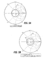
- FIGS. 5A and 5B are Smith charts that illustrate VSWR circles that correspond to power dissipation measurements for an electronic device according to some embodiments
- FIG. 6 is a block diagram illustrating tuning of a tunable matching circuit according to further embodiments.
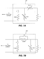
- FIGS. 7A-7C are circuit diagrams illustrating tunable matching circuits according to various embodiments.
- wireless terminal may include a satellite or cellular radiotelephone with or without a multi-line display; a Personal Communications System (PCS) terminal that may combine a cellular radiotelephone with data processing, facsimile and data communications capabilities; a PDA that can include a radiotelephone, pager, Internet/intranet access, Web browser, organizer, calendar and/or a global positioning system (GPS) receiver; and a conventional laptop and/or palmtop receiver or other appliance that includes a radiotelephone transceiver.
- PCS Personal Communications System
- a wireless terminal 100 in accordance with some embodiments of the present invention, includes an audio processor 103, a microphone 110, a keyboard/keypad 115, a speaker 120, a transceiver 130, and a memory 135 that communicate with a processor 110.
- the wireless terminal 100 may alternatively be referred to as a wireless communication device 100.
- the wireless terminal may optionally include a display 125, a camera 105, and/or an accelerometer unit 102.
- the transceiver 130 comprises a transmitter circuit 145 and a receiver circuit 150, which respectively transmit outgoing radio frequency signals to remote transceivers and receive incoming radio frequency signals from the remote transceivers via an antenna 155.
- the radio frequency signals transmitted between the wireless terminal 100 and the remote transceivers may comprise both traffic and control signals (e.g., paging signals/messages for incoming calls), which are used to establish and maintain communication with another party or destination.
- the radio frequency signals may also comprise packet data information, such as, for example, cellular digital packet data (CDPD) information.
- CDPD cellular digital packet data
- the wireless terminal 100 may communicate with base station transceivers using one or more cellular communication protocols such as, for example, Advanced Mobile Phone Service (AMPS), ANSI-136, Global Standard for Mobile (GSM) communication, General Packet Radio Service (GPRS), enhanced data rates for GSM evolution (EDGE), Integrated Digital Enhancement Network (iDEN), code division multiple access (CDMA), wideband-CDMA, CDMA2000, and/or Universal Mobile Telecommunications System (UMTS).
- AMPS Advanced Mobile Phone Service
- GSM Global Standard for Mobile
- GPRS General Packet Radio Service
- EDGE enhanced data rates for GSM evolution
- iDEN Integrated Digital Enhancement Network
- CDMA code division multiple access
- CDMA2000 wideband-CDMA2000
- UMTS Universal Mobile Telecommunications System
- the foregoing components of the wireless terminal 100 may be included in many conventional wireless terminals and their functionality is generally known to those skilled in the art.
- the processor 110 communicates with the memory 135 via an address/data bus.
- the processor 110 may be, for example, a commercially available or custom microprocessor.
- the memory 135 is representative of the one or more memory devices containing the software and data used to operate the wireless terminal 100.
- the memory 135 may include, but is not limited to, the following types of devices: cache, ROM, PROM, EPROM, EEPROM, flash, SRAM, and DRAM.
- the memory 135 may contain an operating system 160 that generally controls the operation of the wireless terminal 100.
- the operating system 165 may manage the wireless terminal's software and/or hardware resources and may coordinate execution of programs by the processor 110.
- a tunable matching network 165 couples the antenna 155 to the transceiver 130.
- the tunable matching network 165 may alternatively be referred to as a tunable matching circuit 165.
- the matching network may be tunable to different impedances so that the impedance of the antenna can be matched to the output impedance of the transceiver as the impedance of the antenna changes due, for example, to changes in the orientation and/or positioning of the antenna.
- FIGS. 2-7C Various embodiments of tunable antenna interface circuits and methods of tuning antenna interface circuits will now be described with reference to FIGS. 2-7C .
- an RF Front end 210 of a transceiver 130 is coupled to the antenna 155 through a directional coupler 220 and tunable matching circuit 165.
- the RF front end 210 may alternatively be referred to as an RF communication unit 210.
- the directional coupler 220 may alternatively be referred to as a power coupler 220.
- the directional coupler 220 includes an input port 220a and an output port 220b, along with a coupled port and an isolated port. Power incident on the coupler 220 (Pi) at the input port 220a can be measured at the coupled port, while power reflected from the load (Pr) at the output port 220b can be measured at the isolated port.
- the RF front end 210 generally includes everything between the antenna and the digital base band system of the transceiver 130.
- Such components may include filters, low-noise amplifiers (LNAs), and down-conversion mixer(s) needed to process the modulated signals received at the antenna into signals suitable for input into the base band analog-to-digital converter (ADC), as well as the filters, up-conversion mixers and power amplifiers used to generate a signal to be transmitted over the antenna.
- LNAs low-noise amplifiers
- ADC base band analog-to-digital converter
- some quantity that describes the current antenna performance may be measured.
- the simplest way of doing this is by measuring the power that is reflected back from the antenna (Pr) at the isolated port of the directional coupler 220. Since most wireless communication devices already have a directional power coupler at the output of the RF front end, it may be convenient to use the coupler to measure both forward and reverse power for purposes of characterizing the antenna performance.
- the power dissipated in the antenna (Pd) is equal to the power (Pi) that is incident on the antenna and matching network less the power (Pr) that is reflected from the antenna and matching network.
- One approach to tuning an antenna matching network involves attempting to maximize the power delivered to the load (i.e., the antenna), or attempting to minimize the power reflected from the antenna.
- a parameter of a tunable matching circuit is iteratively adjusted, either up or down, and the dissipated power is measured until a parameter value that maximizes power dissipation is identified.
- the incident and reflected power (Pi and Pr) are measured, for example at the coupled and isolated ports of a directional power coupler 220, and the power dissipation Pd is calculated (Block 305).
- a parameter of the tunable matching network 165 such as the impedance of the network or of a component in the network, is then adjusted in a first direction (e.g., direction A, which may be up or down) (Block 310).
- the power dissipation Pd is calculated again and compared to the previous calculation. If the power dissipation increases in response to the direction A adjustment, the parameter is again adjusted in direction A, and the power dissipation Pd is again measured/calculated (Block 320). Adjustment in direction A continues until the power dissipation Pd does not increase (e.g., more than a threshold amount) in response to the adjustment, at which point it is assumed that the optimum impedance level has been determined (Block 340).
- the parameter is adjusted in a second direction (direction B) that may be opposite the first direction (Block 330).
- the adjustment in direction B continues until the power dissipation Pd does not increase (e.g., more than a threshold amount) in response to the adjustment, at which point it is assumed that the optimum impedance level has been determined (Block 340).
- an approach as illustrated in FIG. 3 may have several drawbacks.
- the impedance presented to the power amplifier in the RF front end 220 is unknown. Accordingly, there is no way of knowing that the power amplifier passes 3GPP and operator requirements at this load. This method of tuning may be time consuming, and the tuning time is proportional to the accuracy of the tunable match. Furthermore, it may be difficult using this approach to tune with more than one tuning element.
- an impedance value of an antenna may be measured.
- An impedance of a tunable matching network can be set so that a combined impedance of the antenna and the matching network has a desired value.
- the combined impedance of the antenna and the matching network may be about equal to a characteristic impedance of an RF front end of a transceiver.
- the reflection coefficient ⁇ of a system can be calculated in terms of the load impedance Z L and the characteristic impedance Z 0 of a source, such as a transmitter, or in terms of the voltage standing wave ratio (VSWR) of the system.
- a lower reflection coefficient means that more energy is being delivered to the load, while a higher reflection coefficient means that more energy is being reflected from the load.
- Z L Re Z L + i ⁇ Im Z L
- a given VSWR appears as a circle 501 centered at the origin. Note that this is what can be visualized when only measuring Pi and Pr. That is, any load impedance on the circle 501 will result in the same VSWR when power is delivered to the load.
- a known measurement impedance, Zmeas is provided, and the incident/reflected power data can be re-taken, thus creating a second VSWR circle. Since the measurement impedance is known, there will be only one Z L that can generate the new VSWR circle. The actual value of the Zmeas can be characterized accurately over frequency and even temperature and stored in the device 100. The tuning of the antenna will be explained in greater detail below.
- the measurement impedance Zmeas that is used to change the VSWR is an impedance that affects the VSWR enough for it to be measurable, but not so much that it severely affects the antenna performance.
- the measurement impedance Zmeas can be different depending on frequency, and it may include elements connected in series and/or in parallel to the antenna.
- a tunable matching circuit 165 is illustrated in FIG. 4 .
- a measurement impedance Zmeas is connected in parallel with the antenna 155 and a tunable impedance Ztune through a series switch S1.
- the switch S1 can be any kind of switch, and the type of switch is not critical since its performance can be characterized together with the measurement impedance.
- the switch S1 may be controlled by a switch control signal CONTROL ( FIG. 2 ) that may be generated, for example, by the processor 110 ( FIG. 1 ).
- the incident and reflected power Pi and Pr may be measured for the antenna 155 alone, resulting in a first VSWR circle 501 as shown in FIG. 5A .
- the impedance of the antenna 155 Since the characteristics of the measurement impedance are known in advance, it is possible to determine exactly where on the initial VSWR trace drawn in the Smith chart the impedance of the antenna 155 is located. This is simply due to the fact that we know which way the measurement impedance would move us in the Smith chart, and there will be only one starting point that together with the measurement impedance will generate the new VSWR circle 502. This means that the complex impedance of the antenna 155 can be described.
- Equation (2) it is possible to create an expression for the antenna impedance (Z L in Equation (2)).
- Equation (5) an equation system containing two unknowns, Re(Z L ) and lm(Z L ), is presented. All other parameters are known, the
- Z 0 is the characteristic impedance of the system.
- the characteristic impedance can be 50 ⁇ or any other impedance that the RF front end 220 would like presented. The actual impedance will most likely be determined by the power amplifier in the RF front end 220.
- the characteristic impedance Z 0 could be different depending on the frequency, power or any other factor such as battery voltage or temperature. Solving the equation system presented in Equation (5) will generate the actual impedance of the antenna 155.
- the impedance of the matching network can be chosen so that a combined impedance of the matching network and the antenna matches the impedance of the RF front end 220 if at least a two stage tunable match is used. If a one stage tunable match is used, it will be possible to change the impedance to, for instance, a purely resistive load or to reduce/minimize the VSWR under the given conditions.
- antenna tuning that is already active needs to be de-embedded from the load impedance before a new matching impedance is calculated.
- the impedance Ztune in FIG. 4 may be set to a high impedance level.
- the incident and reflected power are measured, for example at the coupled and isolated ports of a directional power coupler 220, and the power dissipation Pd is calculated (Block 405).
- the reflection coefficient ⁇ 1 is also calculated at this time.
- a measurement impedance Zmeas is added to the impedance matching network by activating a switch S1 in response to a switch control signal CONTROL, and a new reflection coefficient ⁇ 2 for the system including the measurement impedance is calculated (Block 410).
- the antenna impedance is then calculated according to Equation (5) (Block 415).
- the systems/method determines if a previously applied tuning is active (Block 420). If so, the previous tuning is deactivated (Block 425). In some cases, it may be possible and/or desirable to deactivate the previous tuning before measuring Pi and Pr without the measurement impedance Zmeas switched into the circuit, although this may result in an undesirable impedance shift that may affect power control and/or modulation performance.
- a new tuning impedance is then calculated and applied (Block 430).
- the tuning process illustrated in FIG. 6 above can either be run continuously, from time to time, or can be triggered by change in the operational mode, orientation or position of the device 100, and/or in response to a change in signaling parameters, such as a change in the transmit frequency and/or in response to a handover.
- the tuning process may be initiated whenever the device 100 is changed from an open position to a closed position, when the device 100 is changed from a handheld mode to a handsfree mode, when an accelerometer unit 102 ( FIG. 1 ) in the device detects that the position of the device has been changed, or in response to any other change in condition of the device 100.
- the measurement impedance has been illustrated as a shunt (parallel) impedance.
- a series measurement impedance could also be used instead of or in addition to the parallel impedance.
- the tunable impedance can include both series and/or parallel elements. In order to ensure sufficient freedom to compensate a range of antenna impedances, one series and one shunt element may be used. Methods of calculating impedance compensation values and the topology and implementation of the tunable matching network are well known to those skilled in the art.
- the method may comprise: Measuring 805 first incident power to the antenna and first reflected power from the antenna in response to an output signal applied to the antenna. Coupling 810 a fixed impedance element to the antenna. Measuring 815 second incident power to the antenna and second reflected power from the fixed impedance element and the antenna in response to an output signal applied to the fixed impedance element and the antenna. Determining 820 an impedance associated with the antenna in response to the first and second incident and reflected power measurements. Coupling 825 a variable impedance element to the antenna, the variable impedance element having an impedance selected in response to the impedance associated with the antenna.
- a combined impedance of the variable impedance element and the antenna may present a predetermined output impedance to the RF communication unit.
- determining 820 an impedance associated with the antenna in response to the first and second incident and reflected power measurements comprises generating 830 a first reflection coefficient in response to the first incident power and the first reflected power, generating 835 a second reflection coefficient in response to the second incident power and the second reflected power, and determining 840 the impedance associated with the antenna in response to the first and second reflection coefficients.
- Z L represents the antenna impedance
- Z 0 represents a characteristic impedance of the RF communication unit
- Zmeas represents the impedance of the fixed impedance element
- ⁇ 1 represents the first reflection coefficient
- ⁇ 2 represents the second reflection coefficient.
- the method may further comprise: Determining 845 if a previous impedance tuning is active and responsively deactivating the previous impedance tuning before coupling the variable impedance element to the antenna.
- measuring 805 the first incident power comprises measuring 850 power at a coupled port of a directional coupler that is coupled to the antenna, and wherein measuring 805 the first reflected power comprises measuring 855 power at an isolated port of the directional coupler.
- the tunable matching circuit 165A illustrated in FIG. 7A includes a first variable impedance element Ztune1 connected in parallel with the antenna impedance Z L , and a second variable impedance element Ztune2 connected in series with the antenna impedance Z L.
- a measurement impedance Zmeas is connected in parallel with the antenna impedance Z L .
- the first variable impedance element Ztune1 may be set to a high impedance level
- the second variable impedance element Ztune2 may be set to a low impedance level.
- the tunable matching circuit 165B illustrated in FIG. 7B includes a first measurement impedance element Zmeas1 connected in parallel with the antenna impedance Z L and activated by a first switch S1 in series with the first measurement impedance element Zmeas1, and a second measurement impedance element Zmeas2 connected in series with the antenna impedance Z L and activated by a second switch S2 in parallel with the second measurement impedance element Zmeas2.
- a measurement impedance Zmeas is connected in parallel with the antenna impedance Z L .
- the first variable switch S1 may be closed, while the second switch S2 may be opened.
- the tunable matching circuit 165C illustrated in FIG. 7C includes both parallel and series measurement impedance elements Zmeas1 and Zmeas2, and both parallel and series tunable impedance elements Ztune1 and Ztune2.
- the examples discussed above are illustrative only, and other configurations are possible for the tunable matching network.
Landscapes
- Engineering & Computer Science (AREA)
- Computer Networks & Wireless Communication (AREA)
- Signal Processing (AREA)
- Transmitters (AREA)
- Transceivers (AREA)
Abstract
Description
- Wireless communication devices typically include an antenna to facilitate the transmission and reception of radio frequency (RF) electromagnetic signals. An antenna has a characteristic impedance, or opposition to the flow of electrical energy, based on its design for a given set of certain operating conditions. In order to maximize the transfer of power to and from the antenna, it is desirable to match the impedance of the antenna to the impedance of the circuit that is driving the antenna. Impedance matching networks are well known tools for matching the impedance of a load, such as an antenna, to a source, such as a radio transceiver.
- However, the actual impedance presented by an antenna can change as the antenna is being used. For example, the impedance of the antenna can change when it is held in different orientations, or when it is held near an external object, such as a user's head or hand.
- The performance of the antenna can also be affected by the operating frequency of the antenna and the mode of operation of the antenna. Furthermore, many wireless terminals can be used in various configurations. For example, wireless mobile telephones may have designs, such as clamshell (flip phone), jackknife and slider configurations that typically include two housings coupled together by a hinge or slide. Such configurations may permit the mobile telephone to operate in an open position or a closed position. Typically, the antenna of the device is oriented in one direction when the device is in the open position and in a different direction when the device is in the closed position.
- Similarly, mobile telephones can be used in a handheld talk position in which the telephone is physically held near the user's head, or a handsfree mode in which the mobile telephone is held near the user's body or is even not held by the user at all. Since antennas for wireless devices typically have limited bandwidth and can only be optimized for one use mode (such as for a handheld talk position), it may be difficult to maintain an effective impedance match for the antenna when, for example, the user places a finger over the antenna.
- Changing the antenna matching in response to changes in the mode of operation of the device is usually called antenna tuning. Presently, antenna tuning involves switching an impedance matching circuit between two different impedances. Switching the impedance match may be used to change the resonant frequency of the antenna in broad band applications or to compensate the antenna match depending on whether the device is being used in an open or closed position. However, such an approach may not provide adequate flexibility in tuning the antenna match to accommodate different types of changes in the operating environment of the device. Component and filter manufacturers are developing filter banks, component banks and even tunable components, such as micro electrical-mechanical (MEMS) devices, that are aimed at improving the process of antenna tuning.
- A wireless communication device according to some embodiments includes a power coupler coupled to the signal output poil of an RF communication unit, and a tunable matching circuit coupled to the power coupler. An antenna may be coupled to the tunable matching circuit. The tunable matching circuit may include a variable impedance element having a variable impedance Ztune. The device further includes a fixed impedance element having a fixed impedance Zmeas, and a switch coupled to the fixed impedance element and configured to controllably switch the fixed impedance element into electrical communication with the power coupler and the tunable matching circuit.
- The variable impedance element and/or the fixed impedance element may be coupled in parallel and/or series with the antenna.
- When the fixed impedance element is coupled in parallel with the antenna, the switch may be coupled in series with the fixed impedance element. When the fixed impedance element is coupled in series with the antenna, the switch may be coupled in parallel with the fixed impedance element.
- The variable impedance element may include a first variable impedance element coupled in parallel with the antenna and a second variable impedance element coupled in series with the antenna.
- The RF communication unit may include a transceiver.
- The power coupler may include an input port, an output port, a coupled port and an isolated port, forward power may be present at the coupled port and reflected power may be present at the isolated port.
- Some embodiments provide methods of tuning an antenna matching circuit in a wireless communication device including an RF communication unit and an antenna. The methods may include measuring first incident power to the antenna and first reflected power from the antenna in response to an output signal applied to the antenna, coupling a fixed impedance clement to the antenna, measuring second incident power to the antenna and second reflected power from the fixed impedance element and the antenna in response to an output signal applied to the fixed impedance element and the antenna, and determining an impedance associated with the antenna in response to the first and second incident and reflected power measurements. A variable impedance element may be coupled to the antenna and may have an impedance selected in response to the impedance associated with the antenna.
- A combined impedance of the variable impedance element and the antenna may present a predetermined output impedance to the RF communication unit.
- Determining an impedance associated with the antenna in response to the first and second incident and reflected power measurements may include generating a first reflection coefficient in response to the first incident power and the first reflected power, generating a second reflection coefficient in response to the second incident power and the second reflected power, and determining the impedance associated with the antenna in response to the first and second reflection coefficients.
- The impedance associated with the antenna may be calculated according to the following equation:

- The methods may further include determining if a previous impedance tuning may be active and responsively deactivating the previous impedance tuning before coupling the variable impedance element to the antenna.
- Measuring the first incident power may include measuring power at a coupled port of a directional coupler that may be coupled to the antenna, and measuring the first reflected power may include measuring power at an isolated port of the directional coupler.
- An antenna interface circuit for a wireless communication device according to some embodiments includes a tunable matching circuit and an antenna coupled to the tunable matching circuit. The tunable matching circuit may include a variable impedance element having a variable impedance Ztune. The interface circuit further includes a fixed impedance element having a fixed impedance Zmeas, and a switch coupled to the fixed impedance element and configured to controllably switch the fixed impedance element into electrical communication with the tunable matching circuit.
- According to embodiments of the antenna interface circuit, the variable impedance element may comprise a first variable impedance element coupled in parallel with the antenna and a second variable impedance element coupled in series with the antenna.
- According to embodiments of the antenna interface circuit, the fixed impedance clement may comprise a first fixed impedance element coupled in parallel with the antenna and a second fixed impedance element coupled in series with the antenna.
- Other features of the present invention will be more readily understood from the following detailed description of specific embodiments thereof when read in conjunction with the accompanying drawings, in which:
-
FIG. 1 is a block diagram that illustrates an electronic device/wireless terminal in accordance with some embodiments of the present invention. -
FIG. 2 is a block diagram that illustrates an RF front end with a tunable matching circuit according to some embodiments. -
FIG. 3 is a block diagram illustrating tuning of a tunable matching circuit according to some embodiments. -
FIG. 4 is a circuit diagram illustrating a tunable matching circuit according to some embodiments. -
FIGS. 5A and 5B are Smith charts that illustrate VSWR circles that correspond to power dissipation measurements for an electronic device according to some embodiments; -
FIG. 6 is a block diagram illustrating tuning of a tunable matching circuit according to further embodiments. -
FIGS. 7A-7C are circuit diagrams illustrating tunable matching circuits according to various embodiments. - While the invention is susceptible to various modifications and alternative forms, specific embodiments thereof are shown by way of example in the drawings and will herein be described in detail. It should be understood, however, that there is no intent to limit the invention to the particular forms disclosed, but on the contrary, the invention is to cover all modifications, equivalents, and alternatives falling within the spirit and scope of the invention as defined by the claims. Like reference numbers signify like elements throughout the description of the figures.
- As used herein, the singular forms "a," "an," and "the" are intended to include the plural forms as well, unless expressly stated otherwise. It should be further understood that the terms "comprises" and/or "comprising" when used in this specification is taken to specify the presence of stated features, integers, steps, operations, elements, and/or components, but does not preclude the presence or addition of one or more other features, integers, steps, operations, elements, components, and/or groups thereof. It will be understood that when an element is referred to as being "connected" or "coupled" to another element, it can be directly connected or coupled to the other element or intervening elements may be present. Furthermore, "connected" or "coupled" as used herein may include wirelessly connected or coupled. As used herein, the term "and/or" includes any and all combinations of one or more of the associated listed items.
- Unless otherwise defined, all terms (including technical and scientific terms) used herein have the same meaning as commonly understood by one of ordinary skill in the art to which this invention belongs. It will be further understood that terms, such as those defined in commonly used dictionaries, should be interpreted as having a meaning that is consistent with their meaning in the context of this specification and the relevant art and will not be interpreted in an idealized or overly formal sense unless expressly so defined herein.
- As used herein, the term "wireless terminal" may include a satellite or cellular radiotelephone with or without a multi-line display; a Personal Communications System (PCS) terminal that may combine a cellular radiotelephone with data processing, facsimile and data communications capabilities; a PDA that can include a radiotelephone, pager, Internet/intranet access, Web browser, organizer, calendar and/or a global positioning system (GPS) receiver; and a conventional laptop and/or palmtop receiver or other appliance that includes a radiotelephone transceiver.
- For purposes of illustration, embodiments of the present invention are described herein in the context of a wireless terminal. It will be understood, however, that the present invention is not limited to such embodiments and may be embodied generally as an electronic device that includes an antenna for wireless communication.
- Referring now to
FIG. 1 , awireless terminal 100, in accordance with some embodiments of the present invention, includes anaudio processor 103, amicrophone 110, a keyboard/keypad 115, aspeaker 120, atransceiver 130, and amemory 135 that communicate with aprocessor 110. Thewireless terminal 100 may alternatively be referred to as awireless communication device 100. The wireless terminal may optionally include adisplay 125, acamera 105, and/or anaccelerometer unit 102. Thetransceiver 130 comprises atransmitter circuit 145 and areceiver circuit 150, which respectively transmit outgoing radio frequency signals to remote transceivers and receive incoming radio frequency signals from the remote transceivers via anantenna 155. For wireless telephony, the radio frequency signals transmitted between thewireless terminal 100 and the remote transceivers may comprise both traffic and control signals (e.g., paging signals/messages for incoming calls), which are used to establish and maintain communication with another party or destination. The radio frequency signals may also comprise packet data information, such as, for example, cellular digital packet data (CDPD) information. In accordance with various embodiments of the present invention, thewireless terminal 100 may communicate with base station transceivers using one or more cellular communication protocols such as, for example, Advanced Mobile Phone Service (AMPS), ANSI-136, Global Standard for Mobile (GSM) communication, General Packet Radio Service (GPRS), enhanced data rates for GSM evolution (EDGE), Integrated Digital Enhancement Network (iDEN), code division multiple access (CDMA), wideband-CDMA, CDMA2000, and/or Universal Mobile Telecommunications System (UMTS). - The foregoing components of the
wireless terminal 100 may be included in many conventional wireless terminals and their functionality is generally known to those skilled in the art. - The
processor 110 communicates with thememory 135 via an address/data bus. Theprocessor 110 may be, for example, a commercially available or custom microprocessor. Thememory 135 is representative of the one or more memory devices containing the software and data used to operate thewireless terminal 100. Thememory 135 may include, but is not limited to, the following types of devices: cache, ROM, PROM, EPROM, EEPROM, flash, SRAM, and DRAM. - As shown in
FIG. 1 , thememory 135 may contain anoperating system 160 that generally controls the operation of thewireless terminal 100. In particular, theoperating system 165 may manage the wireless terminal's software and/or hardware resources and may coordinate execution of programs by theprocessor 110. - A
tunable matching network 165 couples theantenna 155 to thetransceiver 130. Thetunable matching network 165 may alternatively be referred to as atunable matching circuit 165. In some embodiments, the matching network may be tunable to different impedances so that the impedance of the antenna can be matched to the output impedance of the transceiver as the impedance of the antenna changes due, for example, to changes in the orientation and/or positioning of the antenna. Various embodiments of tunable antenna interface circuits and methods of tuning antenna interface circuits will now be described with reference toFIGS. 2-7C . - Referring now to
FIG. 2 which shows elements of a wireless terminal in more detail, an RFFront end 210 of atransceiver 130 is coupled to theantenna 155 through adirectional coupler 220 andtunable matching circuit 165. The RFfront end 210 may alternatively be referred to as anRF communication unit 210. Thedirectional coupler 220 may alternatively be referred to as apower coupler 220. Thedirectional coupler 220 includes aninput port 220a and anoutput port 220b, along with a coupled port and an isolated port. Power incident on the coupler 220 (Pi) at theinput port 220a can be measured at the coupled port, while power reflected from the load (Pr) at theoutput port 220b can be measured at the isolated port. - The RF
front end 210 generally includes everything between the antenna and the digital base band system of thetransceiver 130. Such components may include filters, low-noise amplifiers (LNAs), and down-conversion mixer(s) needed to process the modulated signals received at the antenna into signals suitable for input into the base band analog-to-digital converter (ADC), as well as the filters, up-conversion mixers and power amplifiers used to generate a signal to be transmitted over the antenna. - In order to control the tunable matching network, some quantity that describes the current antenna performance may be measured. The simplest way of doing this is by measuring the power that is reflected back from the antenna (Pr) at the isolated port of the
directional coupler 220. Since most wireless communication devices already have a directional power coupler at the output of the RF front end, it may be convenient to use the coupler to measure both forward and reverse power for purposes of characterizing the antenna performance. - With this setup it is possible to measure the power incident to the load, Pi, the power reflected from the load, Pr, and from these the power delivered to the load can be calculated as follows:

- That is, the power dissipated in the antenna (Pd) is equal to the power (Pi) that is incident on the antenna and matching network less the power (Pr) that is reflected from the antenna and matching network.
- One approach to tuning an antenna matching network, as illustrated in
FIG. 3 , involves attempting to maximize the power delivered to the load (i.e., the antenna), or attempting to minimize the power reflected from the antenna. In such an approach, a parameter of a tunable matching circuit is iteratively adjusted, either up or down, and the dissipated power is measured until a parameter value that maximizes power dissipation is identified. - Referring to
FIG. 3 , the incident and reflected power (Pi and Pr) are measured, for example at the coupled and isolated ports of adirectional power coupler 220, and the power dissipation Pd is calculated (Block 305). A parameter of thetunable matching network 165, such as the impedance of the network or of a component in the network, is then adjusted in a first direction (e.g., direction A, which may be up or down) (Block 310). The power dissipation Pd is calculated again and compared to the previous calculation. If the power dissipation increases in response to the direction A adjustment, the parameter is again adjusted in direction A, and the power dissipation Pd is again measured/calculated (Block 320). Adjustment in direction A continues until the power dissipation Pd does not increase (e.g., more than a threshold amount) in response to the adjustment, at which point it is assumed that the optimum impedance level has been determined (Block 340). - If in
block 315 the power dissipation does not increase in response to the parameter adjustment in direction A, the parameter is adjusted in a second direction (direction B) that may be opposite the first direction (Block 330). The adjustment in direction B continues until the power dissipation Pd does not increase (e.g., more than a threshold amount) in response to the adjustment, at which point it is assumed that the optimum impedance level has been determined (Block 340). - Although straightforward, an approach as illustrated in
FIG. 3 may have several drawbacks. For example, the impedance presented to the power amplifier in the RFfront end 220 is unknown. Accordingly, there is no way of knowing that the power amplifier passes 3GPP and operator requirements at this load. This method of tuning may be time consuming, and the tuning time is proportional to the accuracy of the tunable match. Furthermore, it may be difficult using this approach to tune with more than one tuning element. - In order to select an impedance for the impendance matching network, it is desirable to know the current antenna impedance. However, it may not be possible to determine a unique value for antenna impedance when only knowing the two parameters Pi and Pr.
- Accordingly, some embodiments provide systems, methods and/or apparatus by which an impedance value of an antenna may be measured. An impedance of a tunable matching network can be set so that a combined impedance of the antenna and the matching network has a desired value. For example, the combined impedance of the antenna and the matching network may be about equal to a characteristic impedance of an RF front end of a transceiver.
- Referring to Equation (2) below, the reflection coefficient Γ of a system can be calculated in terms of the load impedance ZL and the characteristic impedance Z0 of a source, such as a transmitter, or in terms of the voltage standing wave ratio (VSWR) of the system. In general, a lower reflection coefficient means that more energy is being delivered to the load, while a higher reflection coefficient means that more energy is being reflected from the load.

- By combining the expression for the reflection coefficient, Γ, and the return loss, RL, shown in Equation (3), it is possible to calculate the VSWR as a function of the known parameters Pr and Pi.


- In order to explain the idea visually the Smith chart will be used for the following examples. Referring to
FIG. 5A , in the Smith chart, a given VSWR appears as acircle 501 centered at the origin. Note that this is what can be visualized when only measuring Pi and Pr. That is, any load impedance on thecircle 501 will result in the same VSWR when power is delivered to the load. - Accordingly, with only Pi and Pr data available, it is only possible to determine that the antenna impedance is somewhere on a particular VSWR circle. It is not possible to tell exactly where on the circle the impedance is located, however. This makes it impossible to calculate the match needed to get the impedance to a desired position.
- According to some embodiments, in order to determine the absolute impedance, ZL, currently presented by the
antenna 155, a known measurement impedance, Zmeas, is provided, and the incident/reflected power data can be re-taken, thus creating a second VSWR circle. Since the measurement impedance is known, there will be only one ZL that can generate the new VSWR circle. The actual value of the Zmeas can be characterized accurately over frequency and even temperature and stored in thedevice 100. The tuning of the antenna will be explained in greater detail below. - The measurement impedance Zmeas that is used to change the VSWR is an impedance that affects the VSWR enough for it to be measurable, but not so much that it severely affects the antenna performance. The measurement impedance Zmeas can be different depending on frequency, and it may include elements connected in series and/or in parallel to the antenna.
- A
tunable matching circuit 165 according to some embodiments is illustrated inFIG. 4 . As shown therein, a measurement impedance Zmeas is connected in parallel with theantenna 155 and a tunable impedance Ztune through a series switch S1. The switch S1 can be any kind of switch, and the type of switch is not critical since its performance can be characterized together with the measurement impedance. The switch S1 may be controlled by a switch control signal CONTROL (FIG. 2 ) that may be generated, for example, by the processor 110 (FIG. 1 ). - With the switch S1 in an open position and the tunable impedance Ztune set at a high impedance level, the incident and reflected power Pi and Pr may be measured for the
antenna 155 alone, resulting in afirst VSWR circle 501 as shown inFIG. 5A . - With the switch S1 in a closed position, Pi and Pr may be measured once again and this time a
new VSWR circle 502 will be generated, as shown inFIG. 5B . - Since the characteristics of the measurement impedance are known in advance, it is possible to determine exactly where on the initial VSWR trace drawn in the Smith chart the impedance of the
antenna 155 is located. This is simply due to the fact that we know which way the measurement impedance would move us in the Smith chart, and there will be only one starting point that together with the measurement impedance will generate thenew VSWR circle 502. This means that the complex impedance of theantenna 155 can be described. - From Equation (2) and Equation (3) above, it is possible to create an expression for the antenna impedance (ZL in Equation (2)). In Equation (5) below, an equation system containing two unknowns, Re(ZL) and lm(ZL), is presented. All other parameters are known, the |Γ1| and |Γ2| are the calculated reflection coefficients in the cases with and without the measurement impedance Zmeas. Z0 is the characteristic impedance of the system. The characteristic impedance can be 50Ω or any other impedance that the RF
front end 220 would like presented. The actual impedance will most likely be determined by the power amplifier in the RFfront end 220. The characteristic impedance Z0 could be different depending on the frequency, power or any other factor such as battery voltage or temperature. Solving the equation system presented in Equation (5) will generate the actual impedance of theantenna 155.
- Once the actual antenna impedance is known, the impedance of the matching network can be chosen so that a combined impedance of the matching network and the antenna matches the impedance of the RF
front end 220 if at least a two stage tunable match is used. If a one stage tunable match is used, it will be possible to change the impedance to, for instance, a purely resistive load or to reduce/minimize the VSWR under the given conditions. - In order for systems/methods as described above to work continuously, antenna tuning that is already active needs to be de-embedded from the load impedance before a new matching impedance is calculated. For example, the impedance Ztune in
FIG. 4 may be set to a high impedance level. - Methods of tuning an antenna according to some embodiments are illustrated in the flowchart of
FIG. 6 . As shown therein, the incident and reflected power (Pi and Pr) are measured, for example at the coupled and isolated ports of adirectional power coupler 220, and the power dissipation Pd is calculated (Block 405). The reflection coefficient Γ1 is also calculated at this time. A measurement impedance Zmeas is added to the impedance matching network by activating a switch S1 in response to a switch control signal CONTROL, and a new reflection coefficient Γ2 for the system including the measurement impedance is calculated (Block 410). The antenna impedance is then calculated according to Equation (5) (Block 415). - The systems/method then determines if a previously applied tuning is active (Block 420). If so, the previous tuning is deactivated (Block 425). In some cases, it may be possible and/or desirable to deactivate the previous tuning before measuring Pi and Pr without the measurement impedance Zmeas switched into the circuit, although this may result in an undesirable impedance shift that may affect power control and/or modulation performance. A new tuning impedance is then calculated and applied (Block 430).
- The tuning process illustrated in
FIG. 6 above can either be run continuously, from time to time, or can be triggered by change in the operational mode, orientation or position of thedevice 100, and/or in response to a change in signaling parameters, such as a change in the transmit frequency and/or in response to a handover. For example, the tuning process may be initiated whenever thedevice 100 is changed from an open position to a closed position, when thedevice 100 is changed from a handheld mode to a handsfree mode, when an accelerometer unit 102 (FIG. 1 ) in the device detects that the position of the device has been changed, or in response to any other change in condition of thedevice 100. - In the examples discussed above, the measurement impedance has been illustrated as a shunt (parallel) impedance. However, a series measurement impedance could also be used instead of or in addition to the parallel impedance. Similarly, the tunable impedance can include both series and/or parallel elements. In order to ensure sufficient freedom to compensate a range of antenna impedances, one series and one shunt element may be used. Methods of calculating impedance compensation values and the topology and implementation of the tunable matching network are well known to those skilled in the art.
- Methods of tuning an
antenna matching circuit 165 in awireless communication device 100 including anRF communication unit 210 and anantenna 155, according to some embodiments are illustrated in the flowchart ofFIG. 8 . As shown therein the method may comprise: Measuring 805 first incident power to the antenna and first reflected power from the antenna in response to an output signal applied to the antenna. Coupling 810 a fixed impedance element to the antenna. Measuring 815 second incident power to the antenna and second reflected power from the fixed impedance element and the antenna in response to an output signal applied to the fixed impedance element and the antenna. Determining 820 an impedance associated with the antenna in response to the first and second incident and reflected power measurements. Coupling 825 a variable impedance element to the antenna, the variable impedance element having an impedance selected in response to the impedance associated with the antenna. - According to embodiments, a combined impedance of the variable impedance element and the antenna may present a predetermined output impedance to the RF communication unit.
- According to embodiments, determining 820 an impedance associated with the antenna in response to the first and second incident and reflected power measurements comprises generating 830 a first reflection coefficient in response to the first incident power and the first reflected power, generating 835 a second reflection coefficient in response to the second incident power and the second reflected power, and determining 840 the impedance associated with the antenna in response to the first and second reflection coefficients.
- According to embodiments the method may comprise the impedance associated with the antenna is calculated according to the following equation:

- According to embodiments the method may further comprise: Determining 845 if a previous impedance tuning is active and responsively deactivating the previous impedance tuning before coupling the variable impedance element to the antenna.
- According to embodiments measuring 805 the first incident power comprises measuring 850 power at a coupled port of a directional coupler that is coupled to the antenna, and wherein measuring 805 the first reflected power comprises measuring 855 power at an isolated port of the directional coupler.
- For example, tunable matching circuits according to various embodiments of the invention are illustrated in
FIGS. 7A to 7C . Thetunable matching circuit 165A illustrated inFIG. 7A includes a first variable impedance element Ztune1 connected in parallel with the antenna impedance ZL, and a second variable impedance element Ztune2 connected in series with the antenna impedance ZL. A measurement impedance Zmeas is connected in parallel with the antenna impedance ZL. In order to deactivate the variable impedance elements, the first variable impedance element Ztune1 may be set to a high impedance level, while the second variable impedance element Ztune2 may be set to a low impedance level. - The
tunable matching circuit 165B illustrated inFIG. 7B includes a first measurement impedance element Zmeas1 connected in parallel with the antenna impedance ZL and activated by a first switch S1 in series with the first measurement impedance element Zmeas1, and a second measurement impedance element Zmeas2 connected in series with the antenna impedance ZL and activated by a second switch S2 in parallel with the second measurement impedance element Zmeas2. A measurement impedance Zmeas is connected in parallel with the antenna impedance ZL. In order to activate the measurement impedance elements, the first variable switch S1 may be closed, while the second switch S2 may be opened. - The
tunable matching circuit 165C illustrated inFIG. 7C includes both parallel and series measurement impedance elements Zmeas1 and Zmeas2, and both parallel and series tunable impedance elements Ztune1 and Ztune2. The examples discussed above are illustrative only, and other configurations are possible for the tunable matching network. - Many variations and modifications can be made to the embodiments without substantially departing from the principles of the present invention. All such variations and modifications are intended to be included herein within the scope of the present invention, as set forth in the following claims.
Claims (15)
- A wireless communication device (100), comprising:a power coupler coupled (220) to a signal output port of an RF communication unit (210);a tunable matching circuit (165) coupled to the power coupler (220) and including a variable impedance element having a variable impedance Ztune;a fixed impedance element having a fixed impedance Zmeas; anda switch (S1; S2) coupled to the fixed impedance element and configured to controllably switch the fixed impedance element into electrical communication with the power coupler (220) and the tunable matching circuit (165).
- The wireless communication device (100) of Claim 1, further comprising an antenna (155) coupled to the tunable matching circuit (165).
- The wireless communication device (100) of Claim 2, wherein the variable impedance element is coupled in parallel with the antenna (155) and/or the variable impedance element is coupled in series with the antenna (155).
- The wireless communication device (100) of any of Claims 2-3, wherein the fixed impedance element is coupled in parallel with the antenna (155).
- The wireless communication device (100) of Claim 4, wherein the switch (S1) is coupled in series with the fixed impedance element.
- The wireless communication device (100) of any of Claims 2-5, wherein the fixed impedance element is coupled in series with the antenna (155).
- The wireless communication device (100) of Claim 6, wherein the switch (S2) is coupled in parallel with the fixed impedance element.
- The wireless communication device (100) of any of Claims 1-7, wherein the power coupler (220) comprises an input port (220a), an output port (220b), a coupled port and an isolated port, wherein forward power is present at the coupled port and reflected power is present at the isolated port.
- A method of tuning an antenna matching circuit (165) in a wireless communication device (100) including an RF communication unit (210) and an antenna (155), the method comprising:measuring (805) first incident power to the antenna and first reflected power from the antenna in response to an output signal applied to the antenna;coupling (810) a fixed impedance element to the antenna;measuring (815) second incident power to the antenna and second reflected power from the fixed impedance element and the antenna in response to an output signal applied to the fixed impedance element and the antenna;determining (820) an impedance associated with the antenna in response to the first and second incident and reflected power measurements; andcoupling (825) a variable impedance element to the antenna, the variable impedance element having an impedance selected in response to the impedance associated with the antenna.
- The method of Claim 9, wherein a combined impedance of the variable impedance element and the antenna present a predetermined output impedance to the RF communication unit.
- The method of any of Claims 9-10, wherein determining (820) an impedance associated with the antenna in response to the first and second incident and reflected power measurements comprises generating (830) a first reflection coefficient in response to the first incident power and the first reflected power, generating (835) a second reflection coefficient in response to the second incident power and the second reflected power, and determining (840) the impedance associated with the antenna in response to the first and second reflection coefficients.
- The method of Claim 11, wherein the impedance associated with the antenna is calculated according to the following equation:

- The method of any of Claims 9-12, further comprising determining (845) if a previous impedance tuning is active and responsively deactivating the previous impedance tuning before coupling the variable impedance element to the antenna.
- The method of any of Claims 9-13, wherein measuring (805) the first incident power comprises measuring (850) power at a coupled port of a directional coupler that is coupled to the antenna, and wherein measuring (805) the first reflected power comprises measuring (855) power at an isolated port of the directional coupler.
- An antenna interface circuit for a wireless communication device (100) including an antenna (155), the circuit comprising:a tunable matching circuit (165) coupled to the antenna (155), wherein the tunable matching circuit (165) comprises a variable impedance clement having a variable impedance Ztune;a fixed impedance element having a fixed impedance Zmeas; anda switch (S1; S2) coupled to the fixed impedance element and configured to controllably switch the fixed impendance element into electrical communication with the tunable matching circuit (165).
Applications Claiming Priority (1)
| Application Number | Priority Date | Filing Date | Title |
|---|---|---|---|
| US12/781,864 US8294632B2 (en) | 2010-05-18 | 2010-05-18 | Antenna interface circuits including tunable impedance matching networks, electronic devices incorporating the same, and methods of tuning antenna interface circuits |
Publications (1)
| Publication Number | Publication Date |
|---|---|
| EP2388925A1 true EP2388925A1 (en) | 2011-11-23 |
Family
ID=44247600
Family Applications (1)
| Application Number | Title | Priority Date | Filing Date |
|---|---|---|---|
| EP11162309A Withdrawn EP2388925A1 (en) | 2010-05-18 | 2011-04-13 | Antenna interface circuits including tunable impedance matching networks, electronic devices incorporating the same, and methods of tuning antenna interface circuits |
Country Status (2)
| Country | Link |
|---|---|
| US (1) | US8294632B2 (en) |
| EP (1) | EP2388925A1 (en) |
Cited By (30)
| Publication number | Priority date | Publication date | Assignee | Title |
|---|---|---|---|---|
| WO2013120536A1 (en) * | 2012-02-17 | 2013-08-22 | Sony Ericsson Mobile Communications Ab | Antenna tunning arrangement and method |
| EP2670052A1 (en) * | 2012-06-01 | 2013-12-04 | BlackBerry Limited | Methods and apparatus for tuning circuit components of a communication device |
| US8712340B2 (en) | 2011-02-18 | 2014-04-29 | Blackberry Limited | Method and apparatus for radio antenna frequency tuning |
| US8744384B2 (en) | 2000-07-20 | 2014-06-03 | Blackberry Limited | Tunable microwave devices with auto-adjusting matching circuit |
| US8781417B2 (en) | 2007-05-07 | 2014-07-15 | Blackberry Limited | Hybrid techniques for antenna retuning utilizing transmit and receive power information |
| US8787845B2 (en) | 2009-08-25 | 2014-07-22 | Blackberry Limited | Method and apparatus for calibrating a communication device |
| US8803631B2 (en) | 2010-03-22 | 2014-08-12 | Blackberry Limited | Method and apparatus for adapting a variable impedance network |
| EP2768147A1 (en) * | 2013-02-14 | 2014-08-20 | BlackBerry Limited | Methods and apparatus for performing impedance matching |
| US8860526B2 (en) | 2010-04-20 | 2014-10-14 | Blackberry Limited | Method and apparatus for managing interference in a communication device |
| US8942657B2 (en) | 2006-01-14 | 2015-01-27 | Blackberry Limited | Adaptive matching network |
| US8957742B2 (en) | 2008-09-24 | 2015-02-17 | Blackberry Limited | Methods for tuning an adaptive impedance matching network with a look-up table |
| US9026062B2 (en) | 2009-10-10 | 2015-05-05 | Blackberry Limited | Method and apparatus for managing operations of a communication device |
| CN104871459A (en) * | 2012-10-30 | 2015-08-26 | 爱立信调制解调器有限公司 | Standing wave ratio meter for integrated antenna tuner |
| US9130543B2 (en) | 2006-11-08 | 2015-09-08 | Blackberry Limited | Method and apparatus for adaptive impedance matching |
| US9246223B2 (en) | 2012-07-17 | 2016-01-26 | Blackberry Limited | Antenna tuning for multiband operation |
| US9263806B2 (en) | 2010-11-08 | 2016-02-16 | Blackberry Limited | Method and apparatus for tuning antennas in a communication device |
| US9350405B2 (en) | 2012-07-19 | 2016-05-24 | Blackberry Limited | Method and apparatus for antenna tuning and power consumption management in a communication device |
| US9362891B2 (en) | 2012-07-26 | 2016-06-07 | Blackberry Limited | Methods and apparatus for tuning a communication device |
| US9374113B2 (en) | 2012-12-21 | 2016-06-21 | Blackberry Limited | Method and apparatus for adjusting the timing of radio antenna tuning |
| US9413066B2 (en) | 2012-07-19 | 2016-08-09 | Blackberry Limited | Method and apparatus for beam forming and antenna tuning in a communication device |
| US9419581B2 (en) | 2006-11-08 | 2016-08-16 | Blackberry Limited | Adaptive impedance matching apparatus, system and method with improved dynamic range |
| US9473216B2 (en) | 2011-02-25 | 2016-10-18 | Blackberry Limited | Method and apparatus for tuning a communication device |
| US9698748B2 (en) | 2007-04-23 | 2017-07-04 | Blackberry Limited | Adaptive impedance matching |
| US9716311B2 (en) | 2011-05-16 | 2017-07-25 | Blackberry Limited | Method and apparatus for tuning a communication device |
| US9769826B2 (en) | 2011-08-05 | 2017-09-19 | Blackberry Limited | Method and apparatus for band tuning in a communication device |
| US9853363B2 (en) | 2012-07-06 | 2017-12-26 | Blackberry Limited | Methods and apparatus to control mutual coupling between antennas |
| US10003393B2 (en) | 2014-12-16 | 2018-06-19 | Blackberry Limited | Method and apparatus for antenna selection |
| US10163574B2 (en) | 2005-11-14 | 2018-12-25 | Blackberry Limited | Thin films capacitors |
| USRE47412E1 (en) | 2007-11-14 | 2019-05-28 | Blackberry Limited | Tuning matching circuits for transmitter and receiver bands as a function of the transmitter metrics |
| US10404295B2 (en) | 2012-12-21 | 2019-09-03 | Blackberry Limited | Method and apparatus for adjusting the timing of radio antenna tuning |
Families Citing this family (19)
| Publication number | Priority date | Publication date | Assignee | Title |
|---|---|---|---|---|
| US8543176B1 (en) * | 2009-12-08 | 2013-09-24 | Cellco Partnership | Method and system for optimizing impedance match in a mobile communication device |
| US9203489B2 (en) | 2010-05-05 | 2015-12-01 | Google Technology Holdings LLC | Method and precoder information feedback in multi-antenna wireless communication systems |
| US9813262B2 (en) | 2012-12-03 | 2017-11-07 | Google Technology Holdings LLC | Method and apparatus for selectively transmitting data using spatial diversity |
| US9591508B2 (en) | 2012-12-20 | 2017-03-07 | Google Technology Holdings LLC | Methods and apparatus for transmitting data between different peer-to-peer communication groups |
| US9979531B2 (en) | 2013-01-03 | 2018-05-22 | Google Technology Holdings LLC | Method and apparatus for tuning a communication device for multi band operation |
| US10229697B2 (en) | 2013-03-12 | 2019-03-12 | Google Technology Holdings LLC | Apparatus and method for beamforming to obtain voice and noise signals |
| CN103337717B (en) | 2013-06-25 | 2015-07-08 | 华为技术有限公司 | Antenna impedance matching device, semi-conductor chip and antenna impedance matching method |
| US9386542B2 (en) | 2013-09-19 | 2016-07-05 | Google Technology Holdings, LLC | Method and apparatus for estimating transmit power of a wireless device |
| EP3487078B1 (en) * | 2013-10-03 | 2022-05-11 | Andrew Wireless Systems GmbH | Interface device providing power management and load termination in distributed antenna system |
| US9549290B2 (en) | 2013-12-19 | 2017-01-17 | Google Technology Holdings LLC | Method and apparatus for determining direction information for a wireless device |
| US9491007B2 (en) | 2014-04-28 | 2016-11-08 | Google Technology Holdings LLC | Apparatus and method for antenna matching |
| US9478847B2 (en) | 2014-06-02 | 2016-10-25 | Google Technology Holdings LLC | Antenna system and method of assembly for a wearable electronic device |
| US9905902B2 (en) | 2014-07-24 | 2018-02-27 | Skyworks Solutions, Inc. | Zero insertion loss directional coupler for wireless transceivers with integrated power amplifiers |
| US9654152B2 (en) * | 2015-03-02 | 2017-05-16 | Ford Global Technologies, Llc | Service provider adaptive vehicle antenna |
| US20170264010A1 (en) * | 2016-03-09 | 2017-09-14 | Futurewei Technologies, Inc. | Apparatus and Method for Impedance Measurement and Adaptive Antenna Tuning |
| US9628135B1 (en) * | 2016-11-14 | 2017-04-18 | Tekcem | Method for automatically adjusting a tunable matching circuit, and automatic tuning system using this method |
| IL288338B2 (en) | 2019-05-28 | 2023-02-01 | Upside Foods Inc | Devices and methods for preparing an edible meat product |
| MX2022006095A (en) | 2019-11-20 | 2022-08-16 | Upside Foods Inc | APPARATUS AND SYSTEMS FOR PREPARING A MEAT PRODUCT. |
| US11981884B2 (en) | 2022-10-17 | 2024-05-14 | Upside Foods, Inc. | Pipe-based bioreactors for producing comestible meat products and methods of using the same |
Citations (4)
| Publication number | Priority date | Publication date | Assignee | Title |
|---|---|---|---|---|
| US4485360A (en) * | 1982-07-16 | 1984-11-27 | Cincinnati Electronics Corporation | Apparatus for and method of impedance matching |
| WO2002084868A1 (en) * | 2001-04-11 | 2002-10-24 | Kyocera Wireless Corporation | Tunable impedance matching circuit |
| US20080106350A1 (en) * | 2006-11-08 | 2008-05-08 | Mckinzie William E | Adaptive impedance matching apparatus, system and method with improved dynamic range |
| WO2008129125A1 (en) * | 2007-04-19 | 2008-10-30 | Pulse Finland Oy | Method and arrangement for matching an antenna |
Family Cites Families (6)
| Publication number | Priority date | Publication date | Assignee | Title |
|---|---|---|---|---|
| US5195045A (en) * | 1991-02-27 | 1993-03-16 | Astec America, Inc. | Automatic impedance matching apparatus and method |
| US5654679A (en) * | 1996-06-13 | 1997-08-05 | Rf Power Products, Inc. | Apparatus for matching a variable load impedance with an RF power generator impedance |
| US5842154A (en) * | 1997-09-15 | 1998-11-24 | Eni Technologies, Inc. | Fuzzy logic tuning of RF matching network |
| US7298091B2 (en) * | 2002-02-01 | 2007-11-20 | The Regents Of The University Of California | Matching network for RF plasma source |
| US6946847B2 (en) * | 2002-02-08 | 2005-09-20 | Daihen Corporation | Impedance matching device provided with reactance-impedance table |
| US6794951B2 (en) * | 2002-08-05 | 2004-09-21 | Veeco Instruments, Inc. | Solid state RF power switching network |
-
2010
- 2010-05-18 US US12/781,864 patent/US8294632B2/en not_active Expired - Fee Related
-
2011
- 2011-04-13 EP EP11162309A patent/EP2388925A1/en not_active Withdrawn
Patent Citations (4)
| Publication number | Priority date | Publication date | Assignee | Title |
|---|---|---|---|---|
| US4485360A (en) * | 1982-07-16 | 1984-11-27 | Cincinnati Electronics Corporation | Apparatus for and method of impedance matching |
| WO2002084868A1 (en) * | 2001-04-11 | 2002-10-24 | Kyocera Wireless Corporation | Tunable impedance matching circuit |
| US20080106350A1 (en) * | 2006-11-08 | 2008-05-08 | Mckinzie William E | Adaptive impedance matching apparatus, system and method with improved dynamic range |
| WO2008129125A1 (en) * | 2007-04-19 | 2008-10-30 | Pulse Finland Oy | Method and arrangement for matching an antenna |
Cited By (69)
| Publication number | Priority date | Publication date | Assignee | Title |
|---|---|---|---|---|
| US8896391B2 (en) | 2000-07-20 | 2014-11-25 | Blackberry Limited | Tunable microwave devices with auto-adjusting matching circuit |
| US9431990B2 (en) | 2000-07-20 | 2016-08-30 | Blackberry Limited | Tunable microwave devices with auto-adjusting matching circuit |
| US8744384B2 (en) | 2000-07-20 | 2014-06-03 | Blackberry Limited | Tunable microwave devices with auto-adjusting matching circuit |
| US9948270B2 (en) | 2000-07-20 | 2018-04-17 | Blackberry Limited | Tunable microwave devices with auto-adjusting matching circuit |
| US9768752B2 (en) | 2000-07-20 | 2017-09-19 | Blackberry Limited | Tunable microwave devices with auto-adjusting matching circuit |
| US10163574B2 (en) | 2005-11-14 | 2018-12-25 | Blackberry Limited | Thin films capacitors |
| US9853622B2 (en) | 2006-01-14 | 2017-12-26 | Blackberry Limited | Adaptive matching network |
| US8942657B2 (en) | 2006-01-14 | 2015-01-27 | Blackberry Limited | Adaptive matching network |
| US10177731B2 (en) | 2006-01-14 | 2019-01-08 | Blackberry Limited | Adaptive matching network |
| US9130543B2 (en) | 2006-11-08 | 2015-09-08 | Blackberry Limited | Method and apparatus for adaptive impedance matching |
| US9722577B2 (en) | 2006-11-08 | 2017-08-01 | Blackberry Limited | Method and apparatus for adaptive impedance matching |
| US10020828B2 (en) | 2006-11-08 | 2018-07-10 | Blackberry Limited | Adaptive impedance matching apparatus, system and method with improved dynamic range |
| US9419581B2 (en) | 2006-11-08 | 2016-08-16 | Blackberry Limited | Adaptive impedance matching apparatus, system and method with improved dynamic range |
| US10050598B2 (en) | 2006-11-08 | 2018-08-14 | Blackberry Limited | Method and apparatus for adaptive impedance matching |
| US9698748B2 (en) | 2007-04-23 | 2017-07-04 | Blackberry Limited | Adaptive impedance matching |
| US8781417B2 (en) | 2007-05-07 | 2014-07-15 | Blackberry Limited | Hybrid techniques for antenna retuning utilizing transmit and receive power information |
| US9119152B2 (en) | 2007-05-07 | 2015-08-25 | Blackberry Limited | Hybrid techniques for antenna retuning utilizing transmit and receive power information |
| USRE47412E1 (en) | 2007-11-14 | 2019-05-28 | Blackberry Limited | Tuning matching circuits for transmitter and receiver bands as a function of the transmitter metrics |
| USRE48435E1 (en) | 2007-11-14 | 2021-02-09 | Nxp Usa, Inc. | Tuning matching circuits for transmitter and receiver bands as a function of the transmitter metrics |
| US9698758B2 (en) | 2008-09-24 | 2017-07-04 | Blackberry Limited | Methods for tuning an adaptive impedance matching network with a look-up table |
| US8957742B2 (en) | 2008-09-24 | 2015-02-17 | Blackberry Limited | Methods for tuning an adaptive impedance matching network with a look-up table |
| US9020446B2 (en) | 2009-08-25 | 2015-04-28 | Blackberry Limited | Method and apparatus for calibrating a communication device |
| US8787845B2 (en) | 2009-08-25 | 2014-07-22 | Blackberry Limited | Method and apparatus for calibrating a communication device |
| US9026062B2 (en) | 2009-10-10 | 2015-05-05 | Blackberry Limited | Method and apparatus for managing operations of a communication device |
| US10659088B2 (en) | 2009-10-10 | 2020-05-19 | Nxp Usa, Inc. | Method and apparatus for managing operations of a communication device |
| US9548716B2 (en) | 2010-03-22 | 2017-01-17 | Blackberry Limited | Method and apparatus for adapting a variable impedance network |
| US9742375B2 (en) | 2010-03-22 | 2017-08-22 | Blackberry Limited | Method and apparatus for adapting a variable impedance network |
| US10263595B2 (en) | 2010-03-22 | 2019-04-16 | Blackberry Limited | Method and apparatus for adapting a variable impedance network |
| US10615769B2 (en) | 2010-03-22 | 2020-04-07 | Blackberry Limited | Method and apparatus for adapting a variable impedance network |
| US8803631B2 (en) | 2010-03-22 | 2014-08-12 | Blackberry Limited | Method and apparatus for adapting a variable impedance network |
| US9608591B2 (en) | 2010-03-22 | 2017-03-28 | Blackberry Limited | Method and apparatus for adapting a variable impedance network |
| US9941922B2 (en) | 2010-04-20 | 2018-04-10 | Blackberry Limited | Method and apparatus for managing interference in a communication device |
| US9450637B2 (en) | 2010-04-20 | 2016-09-20 | Blackberry Limited | Method and apparatus for managing interference in a communication device |
| US8860526B2 (en) | 2010-04-20 | 2014-10-14 | Blackberry Limited | Method and apparatus for managing interference in a communication device |
| US8860525B2 (en) | 2010-04-20 | 2014-10-14 | Blackberry Limited | Method and apparatus for managing interference in a communication device |
| US9263806B2 (en) | 2010-11-08 | 2016-02-16 | Blackberry Limited | Method and apparatus for tuning antennas in a communication device |
| US9379454B2 (en) | 2010-11-08 | 2016-06-28 | Blackberry Limited | Method and apparatus for tuning antennas in a communication device |
| US10979095B2 (en) | 2011-02-18 | 2021-04-13 | Nxp Usa, Inc. | Method and apparatus for radio antenna frequency tuning |
| US8712340B2 (en) | 2011-02-18 | 2014-04-29 | Blackberry Limited | Method and apparatus for radio antenna frequency tuning |
| US9698858B2 (en) | 2011-02-18 | 2017-07-04 | Blackberry Limited | Method and apparatus for radio antenna frequency tuning |
| US9231643B2 (en) | 2011-02-18 | 2016-01-05 | Blackberry Limited | Method and apparatus for radio antenna frequency tuning |
| US9935674B2 (en) | 2011-02-18 | 2018-04-03 | Blackberry Limited | Method and apparatus for radio antenna frequency tuning |
| US9473216B2 (en) | 2011-02-25 | 2016-10-18 | Blackberry Limited | Method and apparatus for tuning a communication device |
| US9716311B2 (en) | 2011-05-16 | 2017-07-25 | Blackberry Limited | Method and apparatus for tuning a communication device |
| US10218070B2 (en) | 2011-05-16 | 2019-02-26 | Blackberry Limited | Method and apparatus for tuning a communication device |
| US10624091B2 (en) | 2011-08-05 | 2020-04-14 | Blackberry Limited | Method and apparatus for band tuning in a communication device |
| US9769826B2 (en) | 2011-08-05 | 2017-09-19 | Blackberry Limited | Method and apparatus for band tuning in a communication device |
| US9088309B2 (en) | 2012-02-17 | 2015-07-21 | Sony Corporation | Antenna tunning arrangement and method |
| WO2013120536A1 (en) * | 2012-02-17 | 2013-08-22 | Sony Ericsson Mobile Communications Ab | Antenna tunning arrangement and method |
| EP2670052A1 (en) * | 2012-06-01 | 2013-12-04 | BlackBerry Limited | Methods and apparatus for tuning circuit components of a communication device |
| US8948889B2 (en) | 2012-06-01 | 2015-02-03 | Blackberry Limited | Methods and apparatus for tuning circuit components of a communication device |
| US9671765B2 (en) | 2012-06-01 | 2017-06-06 | Blackberry Limited | Methods and apparatus for tuning circuit components of a communication device |
| US9853363B2 (en) | 2012-07-06 | 2017-12-26 | Blackberry Limited | Methods and apparatus to control mutual coupling between antennas |
| US9246223B2 (en) | 2012-07-17 | 2016-01-26 | Blackberry Limited | Antenna tuning for multiband operation |
| US9941910B2 (en) | 2012-07-19 | 2018-04-10 | Blackberry Limited | Method and apparatus for antenna tuning and power consumption management in a communication device |
| US9413066B2 (en) | 2012-07-19 | 2016-08-09 | Blackberry Limited | Method and apparatus for beam forming and antenna tuning in a communication device |
| US9350405B2 (en) | 2012-07-19 | 2016-05-24 | Blackberry Limited | Method and apparatus for antenna tuning and power consumption management in a communication device |
| US9362891B2 (en) | 2012-07-26 | 2016-06-07 | Blackberry Limited | Methods and apparatus for tuning a communication device |
| CN104871459A (en) * | 2012-10-30 | 2015-08-26 | 爱立信调制解调器有限公司 | Standing wave ratio meter for integrated antenna tuner |
| CN104871459B (en) * | 2012-10-30 | 2017-05-17 | 瑞典爱立信有限公司 | wireless communication device, base station, RF transmission circuit and related method |
| US9768810B2 (en) | 2012-12-21 | 2017-09-19 | Blackberry Limited | Method and apparatus for adjusting the timing of radio antenna tuning |
| US10404295B2 (en) | 2012-12-21 | 2019-09-03 | Blackberry Limited | Method and apparatus for adjusting the timing of radio antenna tuning |
| US10700719B2 (en) | 2012-12-21 | 2020-06-30 | Nxp Usa, Inc. | Method and apparatus for adjusting the timing of radio antenna tuning |
| US9374113B2 (en) | 2012-12-21 | 2016-06-21 | Blackberry Limited | Method and apparatus for adjusting the timing of radio antenna tuning |
| EP2768147A1 (en) * | 2013-02-14 | 2014-08-20 | BlackBerry Limited | Methods and apparatus for performing impedance matching |
| US9673844B2 (en) | 2013-02-14 | 2017-06-06 | Blackberry Limited | Methods and apparatus for performing impedance matching |
| US9325355B2 (en) | 2013-02-14 | 2016-04-26 | Blackberry Limited | Methods and apparatus for performing impedance matching |
| US10651918B2 (en) | 2014-12-16 | 2020-05-12 | Nxp Usa, Inc. | Method and apparatus for antenna selection |
| US10003393B2 (en) | 2014-12-16 | 2018-06-19 | Blackberry Limited | Method and apparatus for antenna selection |
Also Published As
| Publication number | Publication date |
|---|---|
| US8294632B2 (en) | 2012-10-23 |
| US20110285603A1 (en) | 2011-11-24 |
Similar Documents
| Publication | Publication Date | Title |
|---|---|---|
| US8294632B2 (en) | Antenna interface circuits including tunable impedance matching networks, electronic devices incorporating the same, and methods of tuning antenna interface circuits | |
| US7747226B2 (en) | Portable electronic devices including multi-mode matching circuits and methods of operating the same | |
| US9466872B2 (en) | Tunable dual loop antenna system | |
| US7907094B2 (en) | Portable terminal apparatus | |
| US9054772B2 (en) | Adaptive impedance matching circuit and method for matching for duplex operation standards | |
| EP2044693B1 (en) | Dual autodiplexing antenna | |
| US8086192B2 (en) | Method and system for power control with optimum power efficiency with a multi-port distributed antenna | |
| US7555276B2 (en) | Devices, methods, and computer program products for controlling power transfer to an antenna in a wireless mobile terminal | |
| KR101504811B1 (en) | Method and apparatus for managing interference in a communication device | |
| JP4987718B2 (en) | Load impedance detection circuit | |
| JP2002171190A (en) | Small mobile phone | |
| US8699975B1 (en) | Directional coupler architecture for radio frequency power amplifier | |
| CN110504977A (en) | A kind of multiband impedance matching circuit and radio frequency system | |
| EP1522143A1 (en) | Apparatus and methods for tuning antenna impedance using transmitter and receiver parameters | |
| EP2568531A1 (en) | Mobile wireless communications device including acoustic coupling based impedance adjustment and related methods | |
| AU1648900A (en) | Dual antenna system | |
| US20070173210A1 (en) | Signal processing apparatus | |
| US8698674B2 (en) | Mobile wireless device with multi-band loop antenna and related methods | |
| JP2004363863A (en) | Portable wireless terminal | |
| CN100446438C (en) | Method for reducing radiation load of mobile wireless terminal and mobile wireless terminal | |
| US7218187B2 (en) | Bow tie coupler | |
| JP3425349B2 (en) | Portable wireless devices | |
| JP2007013890A (en) | Wireless communication device | |
| US20260058743A1 (en) | Harmonic Leakage Rejection for Wireless Circuitry | |
| JP4265651B2 (en) | Mobile device |
Legal Events
| Date | Code | Title | Description |
|---|---|---|---|
| 17P | Request for examination filed |
Effective date: 20110413 |
|
| AK | Designated contracting states |
Kind code of ref document: A1 Designated state(s): AL AT BE BG CH CY CZ DE DK EE ES FI FR GB GR HR HU IE IS IT LI LT LU LV MC MK MT NL NO PL PT RO RS SE SI SK SM TR |
|
| AX | Request for extension of the european patent |
Extension state: BA ME |
|
| PUAI | Public reference made under article 153(3) epc to a published international application that has entered the european phase |
Free format text: ORIGINAL CODE: 0009012 |
|
| 17Q | First examination report despatched |
Effective date: 20150715 |
|
| GRAP | Despatch of communication of intention to grant a patent |
Free format text: ORIGINAL CODE: EPIDOSNIGR1 |
|
| INTG | Intention to grant announced |
Effective date: 20161205 |
|
| STAA | Information on the status of an ep patent application or granted ep patent |
Free format text: STATUS: THE APPLICATION IS DEEMED TO BE WITHDRAWN |
|
| 18D | Application deemed to be withdrawn |
Effective date: 20170419 |