EP2388825A2 - Solar cell structure including a silicon carrier containing a by-pass diode - Google Patents
Solar cell structure including a silicon carrier containing a by-pass diode Download PDFInfo
- Publication number
- EP2388825A2 EP2388825A2 EP11166452A EP11166452A EP2388825A2 EP 2388825 A2 EP2388825 A2 EP 2388825A2 EP 11166452 A EP11166452 A EP 11166452A EP 11166452 A EP11166452 A EP 11166452A EP 2388825 A2 EP2388825 A2 EP 2388825A2
- Authority
- EP
- European Patent Office
- Prior art keywords
- solar cell
- carrier
- front side
- type portion
- metallization layer
- Prior art date
- Legal status (The legal status is an assumption and is not a legal conclusion. Google has not performed a legal analysis and makes no representation as to the accuracy of the status listed.)
- Granted
Links
- XUIMIQQOPSSXEZ-UHFFFAOYSA-N Silicon Chemical compound [Si] XUIMIQQOPSSXEZ-UHFFFAOYSA-N 0.000 title claims abstract description 16
- 229910052710 silicon Inorganic materials 0.000 title claims abstract description 16
- 239000010703 silicon Substances 0.000 title claims abstract description 16
- 238000001465 metallisation Methods 0.000 claims description 55
- 238000000034 method Methods 0.000 claims description 29
- 239000000758 substrate Substances 0.000 claims description 17
- 229910052751 metal Inorganic materials 0.000 claims description 11
- 239000002184 metal Substances 0.000 claims description 11
- 238000009413 insulation Methods 0.000 claims description 10
- 230000008878 coupling Effects 0.000 claims description 2
- 238000010168 coupling process Methods 0.000 claims description 2
- 238000005859 coupling reaction Methods 0.000 claims description 2
- 229910021421 monocrystalline silicon Inorganic materials 0.000 claims description 2
- 239000010410 layer Substances 0.000 description 57
- 239000004065 semiconductor Substances 0.000 description 15
- 239000000463 material Substances 0.000 description 13
- 230000015572 biosynthetic process Effects 0.000 description 4
- 239000011247 coating layer Substances 0.000 description 4
- 239000006059 cover glass Substances 0.000 description 4
- 229910052732 germanium Inorganic materials 0.000 description 3
- GNPVGFCGXDBREM-UHFFFAOYSA-N germanium atom Chemical compound [Ge] GNPVGFCGXDBREM-UHFFFAOYSA-N 0.000 description 3
- 229910001218 Gallium arsenide Inorganic materials 0.000 description 2
- 239000002019 doping agent Substances 0.000 description 2
- 238000004519 manufacturing process Methods 0.000 description 2
- 238000012986 modification Methods 0.000 description 2
- 230000004048 modification Effects 0.000 description 2
- 239000002210 silicon-based material Substances 0.000 description 2
- 238000001228 spectrum Methods 0.000 description 2
- 229910045601 alloy Inorganic materials 0.000 description 1
- 239000000956 alloy Substances 0.000 description 1
- 238000000137 annealing Methods 0.000 description 1
- 238000003491 array Methods 0.000 description 1
- 239000000969 carrier Substances 0.000 description 1
- 230000015556 catabolic process Effects 0.000 description 1
- 238000006243 chemical reaction Methods 0.000 description 1
- 238000005229 chemical vapour deposition Methods 0.000 description 1
- 238000010276 construction Methods 0.000 description 1
- 238000006731 degradation reaction Methods 0.000 description 1
- 238000009792 diffusion process Methods 0.000 description 1
- 230000000694 effects Effects 0.000 description 1
- 238000005755 formation reaction Methods 0.000 description 1
- PCHJSUWPFVWCPO-UHFFFAOYSA-N gold Chemical compound [Au] PCHJSUWPFVWCPO-UHFFFAOYSA-N 0.000 description 1
- 229910052737 gold Inorganic materials 0.000 description 1
- 239000010931 gold Substances 0.000 description 1
- 238000005286 illumination Methods 0.000 description 1
- 229910052738 indium Inorganic materials 0.000 description 1
- APFVFJFRJDLVQX-UHFFFAOYSA-N indium atom Chemical compound [In] APFVFJFRJDLVQX-UHFFFAOYSA-N 0.000 description 1
- 230000010354 integration Effects 0.000 description 1
- 150000002739 metals Chemical class 0.000 description 1
- 230000000116 mitigating effect Effects 0.000 description 1
- 229910021420 polycrystalline silicon Inorganic materials 0.000 description 1
- 229910052709 silver Inorganic materials 0.000 description 1
- 239000004332 silver Substances 0.000 description 1
Images



Classifications
-
- H—ELECTRICITY
- H10—SEMICONDUCTOR DEVICES; ELECTRIC SOLID-STATE DEVICES NOT OTHERWISE PROVIDED FOR
- H10F—INORGANIC SEMICONDUCTOR DEVICES SENSITIVE TO INFRARED RADIATION, LIGHT, ELECTROMAGNETIC RADIATION OF SHORTER WAVELENGTH OR CORPUSCULAR RADIATION
- H10F77/00—Constructional details of devices covered by this subclass
- H10F77/95—Circuit arrangements
- H10F77/953—Circuit arrangements for devices having potential barriers
- H10F77/955—Circuit arrangements for devices having potential barriers for photovoltaic devices
-
- H—ELECTRICITY
- H10—SEMICONDUCTOR DEVICES; ELECTRIC SOLID-STATE DEVICES NOT OTHERWISE PROVIDED FOR
- H10F—INORGANIC SEMICONDUCTOR DEVICES SENSITIVE TO INFRARED RADIATION, LIGHT, ELECTROMAGNETIC RADIATION OF SHORTER WAVELENGTH OR CORPUSCULAR RADIATION
- H10F10/00—Individual photovoltaic cells, e.g. solar cells
- H10F10/10—Individual photovoltaic cells, e.g. solar cells having potential barriers
- H10F10/14—Photovoltaic cells having only PN homojunction potential barriers
- H10F10/142—Photovoltaic cells having only PN homojunction potential barriers comprising multiple PN homojunctions, e.g. tandem cells
- H10F10/1425—Inverted metamorphic multi-junction [IMM] photovoltaic cells
-
- H—ELECTRICITY
- H10—SEMICONDUCTOR DEVICES; ELECTRIC SOLID-STATE DEVICES NOT OTHERWISE PROVIDED FOR
- H10F—INORGANIC SEMICONDUCTOR DEVICES SENSITIVE TO INFRARED RADIATION, LIGHT, ELECTROMAGNETIC RADIATION OF SHORTER WAVELENGTH OR CORPUSCULAR RADIATION
- H10F10/00—Individual photovoltaic cells, e.g. solar cells
- H10F10/10—Individual photovoltaic cells, e.g. solar cells having potential barriers
- H10F10/16—Photovoltaic cells having only PN heterojunction potential barriers
- H10F10/161—Photovoltaic cells having only PN heterojunction potential barriers comprising multiple PN heterojunctions, e.g. tandem cells
-
- H—ELECTRICITY
- H10—SEMICONDUCTOR DEVICES; ELECTRIC SOLID-STATE DEVICES NOT OTHERWISE PROVIDED FOR
- H10F—INORGANIC SEMICONDUCTOR DEVICES SENSITIVE TO INFRARED RADIATION, LIGHT, ELECTROMAGNETIC RADIATION OF SHORTER WAVELENGTH OR CORPUSCULAR RADIATION
- H10F10/00—Individual photovoltaic cells, e.g. solar cells
- H10F10/10—Individual photovoltaic cells, e.g. solar cells having potential barriers
- H10F10/16—Photovoltaic cells having only PN heterojunction potential barriers
- H10F10/163—Photovoltaic cells having only PN heterojunction potential barriers comprising only Group III-V materials, e.g. GaAs/AlGaAs or InP/GaInAs photovoltaic cells
-
- H—ELECTRICITY
- H10—SEMICONDUCTOR DEVICES; ELECTRIC SOLID-STATE DEVICES NOT OTHERWISE PROVIDED FOR
- H10F—INORGANIC SEMICONDUCTOR DEVICES SENSITIVE TO INFRARED RADIATION, LIGHT, ELECTROMAGNETIC RADIATION OF SHORTER WAVELENGTH OR CORPUSCULAR RADIATION
- H10F19/00—Integrated devices, or assemblies of multiple devices, comprising at least one photovoltaic cell covered by group H10F10/00, e.g. photovoltaic modules
- H10F19/70—Integrated devices, or assemblies of multiple devices, comprising at least one photovoltaic cell covered by group H10F10/00, e.g. photovoltaic modules comprising bypass diodes
- H10F19/75—Integrated devices, or assemblies of multiple devices, comprising at least one photovoltaic cell covered by group H10F10/00, e.g. photovoltaic modules comprising bypass diodes the bypass diodes being integrated or directly associated with the photovoltaic cells, e.g. formed in or on the same substrate
-
- H—ELECTRICITY
- H10—SEMICONDUCTOR DEVICES; ELECTRIC SOLID-STATE DEVICES NOT OTHERWISE PROVIDED FOR
- H10F—INORGANIC SEMICONDUCTOR DEVICES SENSITIVE TO INFRARED RADIATION, LIGHT, ELECTROMAGNETIC RADIATION OF SHORTER WAVELENGTH OR CORPUSCULAR RADIATION
- H10F71/00—Manufacture or treatment of devices covered by this subclass
- H10F71/127—The active layers comprising only Group III-V materials, e.g. GaAs or InP
-
- H—ELECTRICITY
- H10—SEMICONDUCTOR DEVICES; ELECTRIC SOLID-STATE DEVICES NOT OTHERWISE PROVIDED FOR
- H10F—INORGANIC SEMICONDUCTOR DEVICES SENSITIVE TO INFRARED RADIATION, LIGHT, ELECTROMAGNETIC RADIATION OF SHORTER WAVELENGTH OR CORPUSCULAR RADIATION
- H10F71/00—Manufacture or treatment of devices covered by this subclass
- H10F71/127—The active layers comprising only Group III-V materials, e.g. GaAs or InP
- H10F71/1272—The active layers comprising only Group III-V materials, e.g. GaAs or InP comprising at least three elements, e.g. GaAlAs or InGaAsP
-
- H—ELECTRICITY
- H10—SEMICONDUCTOR DEVICES; ELECTRIC SOLID-STATE DEVICES NOT OTHERWISE PROVIDED FOR
- H10F—INORGANIC SEMICONDUCTOR DEVICES SENSITIVE TO INFRARED RADIATION, LIGHT, ELECTROMAGNETIC RADIATION OF SHORTER WAVELENGTH OR CORPUSCULAR RADIATION
- H10F71/00—Manufacture or treatment of devices covered by this subclass
- H10F71/127—The active layers comprising only Group III-V materials, e.g. GaAs or InP
- H10F71/1276—The active layers comprising only Group III-V materials, e.g. GaAs or InP comprising growth substrates not made of Group III-V materials
-
- H—ELECTRICITY
- H10—SEMICONDUCTOR DEVICES; ELECTRIC SOLID-STATE DEVICES NOT OTHERWISE PROVIDED FOR
- H10F—INORGANIC SEMICONDUCTOR DEVICES SENSITIVE TO INFRARED RADIATION, LIGHT, ELECTROMAGNETIC RADIATION OF SHORTER WAVELENGTH OR CORPUSCULAR RADIATION
- H10F71/00—Manufacture or treatment of devices covered by this subclass
- H10F71/139—Manufacture or treatment of devices covered by this subclass using temporary substrates
-
- Y—GENERAL TAGGING OF NEW TECHNOLOGICAL DEVELOPMENTS; GENERAL TAGGING OF CROSS-SECTIONAL TECHNOLOGIES SPANNING OVER SEVERAL SECTIONS OF THE IPC; TECHNICAL SUBJECTS COVERED BY FORMER USPC CROSS-REFERENCE ART COLLECTIONS [XRACs] AND DIGESTS
- Y02—TECHNOLOGIES OR APPLICATIONS FOR MITIGATION OR ADAPTATION AGAINST CLIMATE CHANGE
- Y02E—REDUCTION OF GREENHOUSE GAS [GHG] EMISSIONS, RELATED TO ENERGY GENERATION, TRANSMISSION OR DISTRIBUTION
- Y02E10/00—Energy generation through renewable energy sources
- Y02E10/50—Photovoltaic [PV] energy
- Y02E10/544—Solar cells from Group III-V materials
-
- Y—GENERAL TAGGING OF NEW TECHNOLOGICAL DEVELOPMENTS; GENERAL TAGGING OF CROSS-SECTIONAL TECHNOLOGIES SPANNING OVER SEVERAL SECTIONS OF THE IPC; TECHNICAL SUBJECTS COVERED BY FORMER USPC CROSS-REFERENCE ART COLLECTIONS [XRACs] AND DIGESTS
- Y02—TECHNOLOGIES OR APPLICATIONS FOR MITIGATION OR ADAPTATION AGAINST CLIMATE CHANGE
- Y02P—CLIMATE CHANGE MITIGATION TECHNOLOGIES IN THE PRODUCTION OR PROCESSING OF GOODS
- Y02P70/00—Climate change mitigation technologies in the production process for final industrial or consumer products
- Y02P70/50—Manufacturing or production processes characterised by the final manufactured product
Definitions
- a first connected pad 144 may be metalized on the front surface 136 of the carrier 102 to electrically contact the N-type portion 130 of the carrier 102 and a second connection pad 146 may be metalized on the front surface 135 of the carrier 102 to electrically contact the P-type portion 128 of the carrier 102.
- Insulation layer 142 may electrically isolate the first connection pad 144 from the P-type portion 128 of the carrier.
- Insulation layer 140 may be applied to the back side 138 of the carrier.
- the solar cell 104 may be initially formed on a temporary substrate 160 with the front side 114 of the solar cell 104 mated with the temporary substrate 160, as shown in Fig. 3 .
- the temporary substrate 160 may be germanium and the solar cell 104 may be an inverted metamorphic solar cell that has been epitaxially grown on the germanium substrate 160, as is known in the art.
- Other techniques may be used to form the solar cell 104 on the temporary substrate 160 without departing from the scope of the present disclosure.
- the method 250 may begin with the separate formation of the carrier 202 (step 252) and the solar cell 204 (step 254).
- the solar cell 204 may be initially formed on a temporary substrate 260 ( Fig. 10 ) in a manner similar to solar cell 104 shown in Fig. 3 .
- a metallization layer 248 ( Fig. 10 ) may be layered over the back side 216 of the solar cell 204. With the metallization of the solar cell 204 complete, the solar cell 204 and associated metallization layer 248 and temporary substrate 260 may be cut to the desired size and shape, a shown in step 264 ( Fig. 14 ).
- the method 250 may proceed to step 266.
- the metallization layer 248 of the solar cell 204 may be connected to metallization layer 244 of the carrier 202 to form the metal-to-metal bond 206 between the solar cell 204 and the carrier 202, as shown in Fig. 10 .
- the temporary carrier 260 may be removed from the solar cell 204, as shown in Fig. 11 .
- step 270 ( Fig.
- the disclosed solar cell structures and methods for assembling solar cell structures provide advantages over the prior art.
- the by-pass diode is used as the manufacturing carrier to support the solar cell, thereby eliminating the need for separate carriers and separate by-pass diodes.
- the integration of the carrier with the by-pass diode may eliminate the need for multiple interconnects.
- the all-front-contact and all-rear-contact configurations simplify implementation and automation of assembly, and the all-front-contact configuration allows for the back side of the carrier to be fully insulated.
- use of a silicon-based carrier significantly reduces material and manufacturing costs, and provides for relatively increased flexibility of the solar cell structures.
Landscapes
- Photovoltaic Devices (AREA)
- Life Sciences & Earth Sciences (AREA)
- Engineering & Computer Science (AREA)
- Sustainable Energy (AREA)
- Sustainable Development (AREA)
Abstract
Description
- This application relates to solar cell structures and, more particularly, to solar cell structures that include a by-pass diode.
- To date, the highest conversion efficiencies achieved for monolithically-grown, series-connected, multi-junction solar cells uses semiconductors with selected energy bandgaps, grown with atomic lattice spacing closely matched to that of the growth substrate. The top two subcells use GaxIn(1-x)P where x is around 0.5, giving bandgap 1.85-1.95eV for the top subcell. The next mid-cell uses InxGa(1-x)As with low In content, providing bandgap 1.38-1.43 eV. Higher efficiencies of the germanium (Ge) subcell is replaced by a subcell with bandgap between 0.95-1.05eV of higher content indium of InxGa(1-x)As. The solar spectrum is more effectively matched if a fourth subcell with lower bandgap is included. These two lower subcells use InxGa(1-x)As where x extends from 0.0 to 0.3. The lattice-mismatch of these lower cells to Ge or GaAs growth substrate can be between 2% and 5%, and can be potentially mitigated by lattice-grading or annealing schedules. The loss in output from lattice-mismatch is offset by the better use of the solar spectrum and the increased voltage. If the lower subcells are grown first, lattice-mismatch reduces the output of the top two cells, which provides 75-85% of the multi-junction cell output. To avoid these mismatch effects on the top two subcells, inverted multi-junction cells are grown, with the top subcells are grown first and lattice closely matched to the Ge or GaAs growth substrate. The lower subcells are grown with mismatched, but the improved energy gap selection can offset the loss in performance resulting from the mismatch, and some mitigation is possible.
- A typical solar cell includes two semiconductor layers in facing contact at a semiconductor junction. When illuminated by the sun or otherwise, the solar cell produces a voltage across the semiconductor layers. More advanced solar cells may include three or more semiconductor layers that define multiple junctions.
- The voltage and current output of a solar cell are limited by the materials of construction and the active surface area of the solar cell structure. Therefore, multiple solar cells are typically electrically interconnected, such as in series, to form a circuit that produces higher voltages than are possible with a single solar cell. A typical solar panel is formed by electrically connecting several circuits, such as in parallel or in series, to produce higher currents or higher voltages. A solar array may be formed as a combination of solar panels. Solar arrays are now used in space and terrestrial applications.
- A circuit of solar cells works well when all of the solar cells are illuminated with generally the same illumination intensity. However, if one of the solar cells is shaded while the others remain fully illuminated, the shaded solar cell is subjected to a reverse-bias condition by the continuing voltage and current output of the remaining solar cells.
- By-pass diodes are used to protect against the damage arising during the reverse-bias condition. A by-pass diode blocks current when the solar cell is not reverse biased, but passes the impressed current when the solar cell is reverse biased.
- While certain techniques for incorporating by-pass diodes into solar cells are known, those skilled in the art continue to seek new ways of incorporating by-pass diodes into solar cell structures.
- Disclosed is a carrier, attached after the growth of the cell layers. The carrier includes suitably patterned P-N junction, which with contacts and bonding methods, provides a bypass diode to each multi-junction cell structure. Several alternative solutions of connecting contacts are given below. All of the advantages of an inverted metamorphic cell are preserved and minimum degradation of performance occurs if shadowing occurs on the solar array.
- In one aspect, the disclosed solar cell structure may include a silicon carrier defining a front side and a back side, and including an N-type portion having an exposed portion on the front side of the carrier and a P-type portion having an exposed portion on the front side of the carrier, the N-type portion and the P-type portion defining a P-N junction, and a solar cell defining a front side and a back side, wherein the solar cell is connected to the front side of the carrier such that the back side of the solar cell is electrically coupled to the exposed portion of the N-type portion, and wherein the front side of the solar cell is electrically coupled to the exposed portion of the P-type portion.
- In another aspect, the disclosed solar cell structure may include a silicon carrier defining a front side and a back side, and comprising an N-type portion having an exposed portion on the front side of the carrier and a P-type portion having an exposed portion on the back side of the carrier, the N-type portion and the P-type portion defining a P-N junction, and a solar cell defining a front side and a back side, wherein the solar cell is connected to the front side of the carrier such that the back side of the solar cell is electrically coupled to the exposed portion of the N-type portion, and a metallization layer that electrically couples the front side of the solar call to the exposed portion of the P-type portion.
- In another aspect, disclosed is a method for assembling a solar cell structure. The method may include the steps of (1) providing a silicon carrier having a front side and a back side, (2) providing a solar cell having a front side and a back side, wherein the back side of the solar cell includes a first metallization layer connected thereto, (3) forming a P-N junction in the carrier such that the carrier includes a P-type portion and an N-type portion, (4) forming a second metallization layer on the front side of the carrier, the second metallization layer being electrically coupled to the N-type portion, (5) connecting the first metallization layer to the second metallization layer to form a metal-to-metal bond between the solar cell and the carrier, and (6) electrically coupling the front side of the solar cell to the P-type portion.
- In yet another aspect, the disclosed method for assembling a solar cell structure may include the steps of (1) providing a silicon carrier having a front side and a back side, (2) providing a solar cell having a front side and a back side, wherein the back side of the solar cell includes a first metallization layer connected thereto, (3) forming a P-N junction in the carrier such that the carrier includes a P-type portion exposed on the back side of said carrier and an N-type portion exposed on the front and the back sides of the carrier, (4) forming a second metallization layer on the front side of the carrier, the second metallization layer being electrically coupled to the N-type portion, (5) connecting the first metallization layer to the second metallization layer to form a metal-to-metal bond between the solar cell and the carrier, and (6) forming a third metallization layer that electrically couples the front side of the solar cell to the P-type portion on the back side of the carrier.
- Other aspects of the disclosed solar cell structure with integral by-pass diode and methods for assembling the same will become apparent from the following description, the accompanying drawings and the appended claims.
-
-
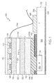
Fig. 1 is a side elevational view, in section, of a first aspect of the disclosed solar cell structure with integral by-pass diode; -
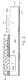
Fig. 2 is a side elevational view, in section, of a carrier of the solar cell structure ofFig. 1 , shown with metallization and insulation layers applied thereto; -
Fig. 3 is a side elevational view, in section, of an inverted metamorphic solar cell used to form the solar cell structure ofFig. 1 ; -
Fig. 4 is a side elevational view, in section, of the inverted metamorphic solar cell ofFig. 3 , shown with an additional metallization layer; -
Fig. 5 is a side elevational view, in section, of the inverted metamorphic solar cell ofFig. 4 connected to the carrier ofFig. 2 during the assembly of the solar cell structure ofFig. 1 in accordance with one aspect of the disclosed method for assembling solar cell structures; -
Fig. 6 is a side elevational view, in section, of the solar cell structure ofFig. 5 , shown with a temporary substrate layer removed therefrom; -
Fig. 7 is a side elevational view, in section, of the solar cell structure ofFig. 1 electrically coupled, in series, to another solar cell structure; -
Fig. 8 is a side elevational view, in section, of a second aspect of the disclosed solar cell structure with integral by-pass diode; -
Fig. 9 is a side elevational view, in section, of a carrier of the solar cell structure ofFig. 8 , shown with metallization layers; -
Fig. 10 is a side elevational view, in section, of the inverted metamorphic solar cell ofFig. 4 connected to the carrier ofFig. 9 during the assembly of the solar cell structure ofFig. 8 in accordance with another aspect of the disclosed method for assembling solar cell structures; -
Fig. 11 is a side elevational view, in section, of the solar cell structure ofFig. 10 , shown with a temporary substrate layer removed therefrom; -
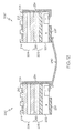
Fig. 12 is a side elevational view, in section, of the solar cell structure ofFig. 8 electrically coupled in series to another solar cell structure; -
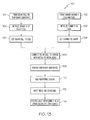
Fig. 13 is a flowchart illustrating a method for assembling the solar cell structure ofFig. 1 ; and -
Fig. 14 is a flowchart illustrating a method for assembling the solar cell structure ofFig. 8 . - Referring to
Fig. 1 , a first aspect of the disclosed solar cell structure, generally designated 100, may include acarrier 102 and asolar cell 104 connected to thecarrier 102 by way of a metal-to-metal bond 106. Thesolar cell structure 100 may also include additional layers, such as a front contact metallization layer 108 (e.g., a grid), ananti-reflecting coating layer 110 and acover glass layer 112, among other possible additional layers. - The
solar cell 104 may include afront side 114 and aback side 116, and may produce a voltage across thefront side 114 and theback side 116 when thefront side 114 is illuminated (e.g., by the sun). Thesolar cell 104 may includemultiple layers junctions solar cell 104 may be an inverted metamorphic solar cell. - The
carrier 102 may include a portion of P-type semiconductor material 128 and a portion of N-type semiconductor material 130, thereby defining aP-N junction 132 in thecarrier 102. Thefront side 114 of thesolar cell 104 may be electrically coupled to the portion of P-type semiconductor material 128 of the carrier 102 (e.g., by way of an interconnect 134) and theback side 116 of thesolar cell 104 may be electrically coupled to the portion of N-type semiconductor material 130 of thecarrier 102, thereby advantageously configuring thecarrier 102 as a diode, specifically, a by-pass diode. - In one particular implementation, the
carrier 102 may be a generally flat, planar structure, such as a wafer, and may include afront side 136 and aback side 138. Both the P-type portion 128 and the N-type portion 130 of thecarrier 102 may be exposed on thefront side 136 of thecarrier 102. Theback side 138 of thecarrier 102 may include a first layer ofinsulation 140. A second layer ofinsulation 142 may be provided on a portion of thefront side 136 of thecarrier 102 to electrically isolate theback side 116 of thesolar cell 104 from the P-type portion 128 of thecarrier 102. - Thus, as shown in
Fig. 7 , thesolar cell structure 100 may be arranged in an array with other like solar cell structures 100' by usinginterconnects 134 in an all-front-contact configuration to electrically couple thefront side 114 of thesolar cell 104 and the P-type portion 128 ofsolar cell structure 100 with theback side 116 of thesolar cell 104 of an adjacent solar cell structure 100'. - One aspect of the disclosed method for forming
solar cell structure 100 is illustrated inFig. 13 and generally designated 150. Themethod 150 may begin with the separate formation of the carrier 102 (step 152) and the solar cell 104 (step 154). - The carrier 102 (
Fig. 1 ) may be formed from a silicon material, such as single crystal silicon or polycrystalline silicon. At this point, those skilled in the art will appreciate that the use of a silicon material to form thecarrier 102 may be advantageous for numerous reasons, including the low cost of silicon, the relative flexibility of silicon, the ease of forming P-N junctions in silicon, among other reasons. - The
P-N junction 132 in thecarrier 102 may be formed using any available technique, including diffusion techniques and growth techniques (e.g., chemical vapor deposition). In one example, thecarrier 102 may be formed by starting with a P-type silicon wafer and diffusing a dopant relative to the P-type silicon wafer to form the portion of N-type semiconductor material 130 on the wafer and, thus, theP-N junction 132. In another example, thecarrier 102 may be formed by starting with an N-type silicon wafer and diffusing a dopant relative to the N-type silicon wafer to form the portion of P-type semiconductor material 128 and, thus, theP-N junction 132. - Once the
carrier 102 has been formed in step 152 (Fig. 13 ), the method may proceed to step 156 (Fig. 13 ), wherein metallization layers may be formed on thecarrier 102. Specifically, referring toFig. 2 , a firstconnected pad 144 may be metalized on thefront surface 136 of thecarrier 102 to electrically contact the N-type portion 130 of thecarrier 102 and asecond connection pad 146 may be metalized on the front surface 135 of thecarrier 102 to electrically contact the P-type portion 128 of thecarrier 102.Insulation layer 142 may electrically isolate thefirst connection pad 144 from the P-type portion 128 of the carrier.Insulation layer 140 may be applied to theback side 138 of the carrier. - With the formation, metallization and insulation of
carrier 102 complete, thecarrier 102 may be cut to the desired shape and size, as shown in step 158 (Fig. 13 ). - At step 154 (
Fig. 13 ), thesolar cell 104 may be initially formed on atemporary substrate 160 with thefront side 114 of thesolar cell 104 mated with thetemporary substrate 160, as shown inFig. 3 . For example, thetemporary substrate 160 may be germanium and thesolar cell 104 may be an inverted metamorphic solar cell that has been epitaxially grown on thegermanium substrate 160, as is known in the art. Other techniques may be used to form thesolar cell 104 on thetemporary substrate 160 without departing from the scope of the present disclosure. - At step 162 (
Fig. 13 ), ametallization layer 148 may be layered over theback side 116 of thesolar cell 104, as shown inFig. 4 . While metallization layers are well known in the art, examples of appropriate materials formetallization layer 144 and metalizedconnection pads solar cell 104 complete, thesolar cell 104 and associatedmetallization layer 148 andtemporary substrate 160 may be cut to the desired size and shape, a shown in step 164 (Fig. 13 ). - Once the
carrier 102 and thesolar cell 104 have been separately formed, the method 150 (Fig. 13 ) may proceed to step 166. Atstep 166, themetallization layer 148 of thesolar cell 104 may be connected to thefirst connection pad 144 of thecarrier 102 to form the metal-to-metal bond 106 between thesolar cell 104 and thecarrier 102, as shown inFig. 5 . At step 168 (Fig. 13 ), thetemporary carrier 160 may be removed from thesolar cell 104, as shown inFig. 6 . The removal of thetemporary carrier 160 may be effected using any technique known or available in the art. At step 170 (Fig. 13 ), the additional layers, such as the frontcontact metallization layer 108, theanti-reflecting coating layer 110 and thecover glass layer 112, may be layered over thefront side 114 of thesolar cell 104, as shown inFig. 1 . Then, at step 172 (Fig. 13 ), the assembly may be heat treated (e.g., sintered) to form the completedsolar cell structure 100. - At
step 174, the completedsolar cell structure 100 may be electrically coupled (e.g., in series) with othersolar cell structures 100 by way of theinterconnect 134, as shown inFig. 7 and described above. - Referring to
Fig. 8 , a second aspect of the disclosed solar cell structure, generally designated 200, may include acarrier 202 and asolar cell 204 connected to thecarrier 202 by way of a metal-to-metal bond 206. Thesolar cell structure 200 may also include additional layers, such as a front contact metallization layer 208 (e.g., a grid), ananti-reflecting coating layer 210 and acover glass layer 212, among other possible additional layers. - The
solar cell 204 may include afront side 214 and aback side 216, and may produce a voltage across thefront side 214 and theback side 216 when thefront side 214 is illuminated. Thesolar cell 204 may includemultiple layers junctions solar cell 104, in one particular implementation,solar cell 204 may be an inverted metamorphic solar cell. - The
carrier 202 may include afront side 236, aback side 238, a portion of P-type semiconductor material 228 and a portion of N-type semiconductor material 230. The P-type portion 228 and the N-type portion 230 of the carrier define at least oneP-N junction 232 in thecarrier 102. - Both the P-
type portion 228 and the N-type portion 230 of thecarrier 202 may be exposed on theback side 238 of thecarrier 202. Thefront side 214 of thesolar cell 204 may be electrically coupled to the P-type portion 228 of thecarrier 202 by way of a wrap-aroundmetallization layer 234, which may be electrically isolated from theback side 216 of thesolar cell 204 by way of aninsulation layer 235. Theback side 216 of thesolar cell 204 may be electrically coupled to the N-type portion 230 of thecarrier 202 by way of the metal-to-metal bond 206. Therefore, thecarrier 202 may advantageously function as a by-pass diode. - Optionally, an additional metallization layer 237 (e.g., a connection pad) may be provided on the
back side 238 of the carrier and may be electrically coupled to the N-type portion 230 of thecarrier 202. - Thus, as shown in
Fig. 12 , thesolar cell structure 200 may be arranged in an array with other like solar cell structures 200' by usinginterconnects 240 in an all-rear-contact configuration to electrically couple thefront side 214 of thesolar cell 204 ofsolar cell structure 200 with theback side 216 of thesolar cell 204 of an adjacent solar cell structure 200' by way of thecarrier 202. - One aspect of the disclosed method for forming
solar cell structure 200 is illustrated inFig. 14 and generally designated 250. Themethod 250 may begin with the separate formation of the carrier 202 (step 252) and the solar cell 204 (step 254). - At
step 252,carrier 202 may be formed with aP-N junction 232 in the same or similar manner ascarrier 202. Once thecarrier 202 has been formed, the method may proceed to step 256 (Fig. 14 ), wherein a first metallization layer 244 (e.g., a first connection pad) may be formed on thefront side 236 of thecarrier 202 and a second metallization layer 237 (e.g., a second connection pad) may be formed on theback side 238 of thecarrier 202. Both the first 244 and the second 237 metallization layers may be electrically coupled to the N-type portion 230 of thecarrier 202. - With the formation and metallization of the
carrier 202 complete, thecarrier 202 may be cut to the desired shape and size, as shown instep 258. - Regarding step 254 (
Fig. 14 ), thesolar cell 204 may be initially formed on a temporary substrate 260 (Fig. 10 ) in a manner similar tosolar cell 104 shown inFig. 3 . Likewise, at step 262 (Fig. 14 ), a metallization layer 248 (Fig. 10 ) may be layered over theback side 216 of thesolar cell 204. With the metallization of thesolar cell 204 complete, thesolar cell 204 and associatedmetallization layer 248 andtemporary substrate 260 may be cut to the desired size and shape, a shown in step 264 (Fig. 14 ). - Once the
carrier 202 and thesolar cell 204 have been separately formed, the method 250 (Fig. 14 ) may proceed to step 266. Atstep 266, themetallization layer 248 of thesolar cell 204 may be connected tometallization layer 244 of thecarrier 202 to form the metal-to-metal bond 206 between thesolar cell 204 and thecarrier 202, as shown inFig. 10 . At step 268 (Fig. 14 ), thetemporary carrier 260 may be removed from thesolar cell 204, as shown inFig. 11 . At step 270 (Fig. 14 ),insulation layer 235 and wrap-aroundmetallization layer 234 may be applied to electrically couple thefront side 214 of thesolar cell 204 with the exposed P-type portion 228 of thecarrier 202, as shown inFig. 8 . At step 272 (Fig. 14 ), the additional layers, such as the frontcontact metallization layer 208, theanti-reflecting coating layer 210 and thecover glass layer 212, may be layered over thefront side 214 of thesolar cell 204, as shown inFig. 8 . Then, at step 274 (Fig. 14 ), the assembly may be heat treated (e.g., sintered) to form the completedsolar cell structure 200. - At
step 276, the completedsolar cell structure 200 may be electrically coupled (e.g., in series) with other solar cell structures 200' by way of theinterconnect 240, as shown inFig. 12 and described above. - At this point, those skilled in the art will appreciate that the disclosed solar cell structures and methods for assembling solar cell structures provide advantages over the prior art. As one advantage, the by-pass diode is used as the manufacturing carrier to support the solar cell, thereby eliminating the need for separate carriers and separate by-pass diodes. As another advantage, the integration of the carrier with the by-pass diode may eliminate the need for multiple interconnects. As another advantage, the all-front-contact and all-rear-contact configurations simplify implementation and automation of assembly, and the all-front-contact configuration allows for the back side of the carrier to be fully insulated. In yet another advantage, use of a silicon-based carrier significantly reduces material and manufacturing costs, and provides for relatively increased flexibility of the solar cell structures.
- Although various aspects of the disclosed solar cell structure with integral by-pass diode have been shown and described, modifications may occur to those skilled in the art upon reading the specification. The present application includes such modifications and is limited only by the scope of the claims.
Claims (14)
- A solar cell structure comprising:a silicon carrier defining a front side and a back side, and comprising an N-type portion having an exposed portion on said front side of said carrier and a P-type portion having an exposed portion on said front side of said carrier, said N-type portion and said P-type portion defining a P-N junction; anda solar cell defining a front side and a back side, wherein said solar cell is connected to said front side of said carrier such that said back side of said solar cell is electrically coupled to said exposed portion of said N-type portion.
- The solar cell structure of claim 1, wherein said front side of said solar cell is electrically coupled to said exposed portion of said P-type portion.
- The solar cell structure of claim 1 or 2 wherein said carrier is formed from single crystal silicon;
or wherein said solar cell comprises an inverted metamorphic solar cell;
or wherein said solar cell is connected to said front side of said carrier by a metal-to-metal bond. - The solar cell structure of claim 1 or 2 further comprising an interconnect that electrically couples said front side of said solar cell to said exposed portion of said P-type portion.
- The solar cell structure of claim 1 or 2 further comprising a first metallization layer positioned over said exposed portion of said N-type portion and a second metallization layer positioned over said exposed portion of said P-type portion.
- The solar cell structure of claim 1 or 2 wherein said back side of said carrier includes an insulation layer connected thereto.
- The solar cell structure of any of claims 1 to 5 and further comprising:a metallization layer that electrically couples said front side of said solar call to said exposed portion of said P-type portion.
- The solar cell structure of claim 7 further comprising an insulation layer positioned to electrically isolate said metallization layer from said back side of said solar cell and said N-type portion.
- The solar cell structure of claim 7 wherein said N-type portion includes a second exposed portion on said back side of said carrier, and wherein a second metallization layer is positioned over said second exposed portion.
- The solar cell structure of claim 9 wherein said metallization layer is electrically coupled to a first adjacent solar cell structure by way of a first interconnect and said second metallization layer is electrically coupled to a second adjacent solar cell structure by way of a second interconnect.
- An array of the solar cell structures of any preceding claim interconnected in series.
- A method for assembling a solar cell structure comprising the steps of:providing a silicon carrier having a front side and a back side;providing a solar cell having a front side and a back side, wherein said back side of said solar cell includes a first metallization layer connected thereto;forming a P-N junction in said carrier such that said carrier includes a P-type portion and an N-type portion;forming a second metallization layer on said front side of said carrier, said second metallization layer being electrically coupled to said N-type portion;connecting said first metallization layer to said second metallization layer to form a metal-to-metal bond therebetween; andelectrically coupling said front side of said solar cell to said P-type portion.
- The method of claim 12 wherein said front side of said solar cell includes a temporary substrate connected thereto, and wherein said method further comprises the step of removing said temporary substrate from said front side of said solar cell after said connecting step.
- The method of claim 12, wherein:said front side of said solar cell includes a temporary substrate connected thereto;forming said P-N junction in said carrier is such that said carrier includes said P-type portion exposed on said back side of said carrier and said N-type portion exposed on said front and said back sides of said carrier; andconnecting said first metallization layer to said second metallization layer forms a metal-to-metal bond between said solar cell and said carrier; andwherein the method further comprises, after said connecting step, removing said temporary substrate from said front side of said solar cell, and forming a third metallization layer that electrically couples said front side of said solar cell to said P-type portion.
Applications Claiming Priority (1)
| Application Number | Priority Date | Filing Date | Title |
|---|---|---|---|
| US12/781,219 US8878048B2 (en) | 2010-05-17 | 2010-05-17 | Solar cell structure including a silicon carrier containing a by-pass diode |
Publications (3)
| Publication Number | Publication Date |
|---|---|
| EP2388825A2 true EP2388825A2 (en) | 2011-11-23 |
| EP2388825A3 EP2388825A3 (en) | 2013-03-06 |
| EP2388825B1 EP2388825B1 (en) | 2020-02-19 |
Family
ID=44544003
Family Applications (1)
| Application Number | Title | Priority Date | Filing Date |
|---|---|---|---|
| EP11166452.0A Active EP2388825B1 (en) | 2010-05-17 | 2011-05-17 | Method of assembling a solar cell structure including a silicon carrier containing a by-pass diode |
Country Status (2)
| Country | Link |
|---|---|
| US (1) | US8878048B2 (en) |
| EP (1) | EP2388825B1 (en) |
Cited By (1)
| Publication number | Priority date | Publication date | Assignee | Title |
|---|---|---|---|---|
| WO2014154769A1 (en) * | 2013-03-29 | 2014-10-02 | Soitec | Advanced cpv solar cell assembly process |
Families Citing this family (6)
| Publication number | Priority date | Publication date | Assignee | Title |
|---|---|---|---|---|
| US20120118383A1 (en) * | 2010-11-15 | 2012-05-17 | International Business Machines Corporation | Autonomous Integrated Circuit |
| DE102011000418A1 (en) * | 2011-01-31 | 2012-08-02 | Azur Space Solar Power Gmbh | Photovoltaic module |
| US9219171B2 (en) | 2012-10-16 | 2015-12-22 | Solexel, Inc. | Systems and methods for monolithically integrated bypass switches in photovoltaic solar cells and modules |
| US10230012B2 (en) * | 2015-08-27 | 2019-03-12 | The Boeing Company | Concentrator photovoltaic cells bonded to flat-plate solar cells for direct and off-axis light collection |
| US11581446B2 (en) * | 2015-10-08 | 2023-02-14 | The Boeing Company | Semiconductor device including an electrically conductive adhesive layer and a bypass diode in a carrier |
| FR3042644B1 (en) * | 2015-10-19 | 2017-12-15 | Commissariat Energie Atomique | PHOTOVOLTAIC CELL WITH DERIVATION DIODE |
Family Cites Families (36)
| Publication number | Priority date | Publication date | Assignee | Title |
|---|---|---|---|---|
| US4152535A (en) | 1976-07-06 | 1979-05-01 | The Boeing Company | Continuous process for fabricating solar cells and the product produced thereby |
| US4392451A (en) | 1980-12-31 | 1983-07-12 | The Boeing Company | Apparatus for forming thin-film heterojunction solar cells employing materials selected from the class of I-III-VI2 chalcopyrite compounds |
| USRE31968E (en) | 1980-12-31 | 1985-08-13 | The Boeing Company | Methods for forming thin-film heterojunction solar cells from I-III-VI.sub.2 |
| JPS6167968A (en) | 1984-09-11 | 1986-04-08 | Sharp Corp | Gaas solar cell element |
| US4833317A (en) | 1987-09-03 | 1989-05-23 | The Boeing Company | Optically powered resolver |
| JPH01205472A (en) * | 1988-02-10 | 1989-08-17 | Mitsubishi Electric Corp | Solar battery cell |
| DE68923061T2 (en) | 1988-11-16 | 1995-11-09 | Mitsubishi Electric Corp | Solar cell. |
| US5217539A (en) | 1991-09-05 | 1993-06-08 | The Boeing Company | III-V solar cells and doping processes |
| US5248346A (en) | 1989-04-17 | 1993-09-28 | The Boeing Company | Photovoltaic cell and array with inherent bypass diode |
| US5389158A (en) | 1989-04-17 | 1995-02-14 | The Boeing Company | Low bandgap photovoltaic cell with inherent bypass diode |
| JP2912496B2 (en) * | 1991-09-30 | 1999-06-28 | シャープ株式会社 | Solar cell module |
| US5543627A (en) | 1994-09-23 | 1996-08-06 | The Boeing Company | Method for maximizing the solar cell OPTO-electronic conversion efficiency in optically controlled hydraulic actuators |
| US5928437A (en) | 1995-02-09 | 1999-07-27 | The Boeing Company | Microarray for efficient energy generation for satellites |
| US5616185A (en) * | 1995-10-10 | 1997-04-01 | Hughes Aircraft Company | Solar cell with integrated bypass diode and method |
| US5949212A (en) | 1997-06-05 | 1999-09-07 | The Boeing Company | Integrated solar cell array and power regulator |
| US6248948B1 (en) * | 1998-05-15 | 2001-06-19 | Canon Kabushiki Kaisha | Solar cell module and method of producing the same |
| US6150603A (en) | 1999-04-23 | 2000-11-21 | Hughes Electronics Corporation | Bilayer passivation structure for photovoltaic cells |
| US6313396B1 (en) | 2000-05-22 | 2001-11-06 | The Boeing Company | Lightweight solar module and method of fabrication |
| US6586669B2 (en) | 2001-06-06 | 2003-07-01 | The Boeing Company | Lattice-matched semiconductor materials for use in electronic or optoelectronic devices |
| US6531653B1 (en) | 2001-09-11 | 2003-03-11 | The Boeing Company | Low cost high solar flux photovoltaic concentrator receiver |
| US7082019B2 (en) | 2002-11-04 | 2006-07-25 | The Boeing Company | Method and apparatus to protect solar cells from electrostatic discharge damage |
| US7335835B2 (en) | 2002-11-08 | 2008-02-26 | The Boeing Company | Solar cell structure with by-pass diode and wrapped front-side diode interconnection |
| US6784358B2 (en) | 2002-11-08 | 2004-08-31 | The Boeing Co. | Solar cell structure utilizing an amorphous silicon discrete by-pass diode |
| US6951819B2 (en) | 2002-12-05 | 2005-10-04 | Blue Photonics, Inc. | High efficiency, monolithic multijunction solar cells containing lattice-mismatched materials and methods of forming same |
| US7592536B2 (en) * | 2003-10-02 | 2009-09-22 | The Boeing Company | Solar cell structure with integrated discrete by-pass diode |
| US20060021565A1 (en) | 2004-07-30 | 2006-02-02 | Aonex Technologies, Inc. | GaInP / GaAs / Si triple junction solar cell enabled by wafer bonding and layer transfer |
| DE102004044061A1 (en) * | 2004-09-11 | 2006-04-20 | Rwe Space Solar Power Gmbh | Solar cell arrangement and method for interconnecting a solar cell string |
| US7732706B1 (en) * | 2004-09-17 | 2010-06-08 | The United States Of America As Represented By The Administrator Of The National Aeronautics And Space Administration | Solar cell circuit and method for manufacturing solar cells |
| DE102004055225B4 (en) * | 2004-11-16 | 2014-07-31 | Fraunhofer-Gesellschaft zur Förderung der angewandten Forschung e.V. | Arrangement with solar cell and integrated bypass diode |
| US7659474B2 (en) | 2005-05-04 | 2010-02-09 | The Boeing Company | Solar cell array with isotype-heterojunction diode |
| US9029685B2 (en) | 2005-11-18 | 2015-05-12 | The Boeing Company | Monolithic bypass diode and photovoltaic cell with bypass diode formed in back of substrate |
| US20090078308A1 (en) * | 2007-09-24 | 2009-03-26 | Emcore Corporation | Thin Inverted Metamorphic Multijunction Solar Cells with Rigid Support |
| US20080149173A1 (en) | 2006-12-21 | 2008-06-26 | Sharps Paul R | Inverted metamorphic solar cell with bypass diode |
| US20090025778A1 (en) * | 2007-07-23 | 2009-01-29 | Day4 Energy Inc. | Shading protection for solar cells and solar cell modules |
| US20090223555A1 (en) | 2008-03-05 | 2009-09-10 | Stalix Llc | High Efficiency Concentrating Photovoltaic Module Method and Apparatus |
| US8283558B2 (en) | 2009-03-27 | 2012-10-09 | The Boeing Company | Solar cell assembly with combined handle substrate and bypass diode and method |
-
2010
- 2010-05-17 US US12/781,219 patent/US8878048B2/en not_active Expired - Fee Related
-
2011
- 2011-05-17 EP EP11166452.0A patent/EP2388825B1/en active Active
Non-Patent Citations (1)
| Title |
|---|
| None |
Cited By (3)
| Publication number | Priority date | Publication date | Assignee | Title |
|---|---|---|---|---|
| WO2014154769A1 (en) * | 2013-03-29 | 2014-10-02 | Soitec | Advanced cpv solar cell assembly process |
| FR3004002A1 (en) * | 2013-03-29 | 2014-10-03 | Soitec Silicon On Insulator | PROCESS FOR ADVANCED ASSEMBLY OF CONCENTRATED PHOTOVOLTAIC CELL |
| US10361326B2 (en) | 2013-03-29 | 2019-07-23 | Soitec | Advanced CPV solar cell assembly process |
Also Published As
| Publication number | Publication date |
|---|---|
| EP2388825B1 (en) | 2020-02-19 |
| US20110277820A1 (en) | 2011-11-17 |
| US8878048B2 (en) | 2014-11-04 |
| EP2388825A3 (en) | 2013-03-06 |
Similar Documents
| Publication | Publication Date | Title |
|---|---|---|
| US9287431B2 (en) | Superstrate sub-cell voltage-matched multijunction solar cells | |
| US9087948B1 (en) | Manufacturing method of multi-junction PV modules | |
| EP1775778B2 (en) | Reliable interconnection of solar cells including integral bypass diode | |
| US7863515B2 (en) | Thin-film solar cell and method of manufacturing the same | |
| EP2412032B1 (en) | Solar cell assembly with combined handle substrate and bypass diode and method | |
| US8766087B2 (en) | Window structure for solar cell | |
| CN103534804B (en) | Apparatus and methods for hybrid photovoltaic devices with multi-stacked hetero-semiconductor junctions | |
| US20100186804A1 (en) | String Interconnection of Inverted Metamorphic Multijunction Solar Cells on Flexible Perforated Carriers | |
| EP2388825B1 (en) | Method of assembling a solar cell structure including a silicon carrier containing a by-pass diode | |
| US20150340528A1 (en) | Monolithic tandem voltage-matched multijuntion solar cells | |
| US9818901B2 (en) | Wafer bonded solar cells and fabrication methods | |
| WO2002049119A2 (en) | Thin film flexible solar cell | |
| US20100132760A1 (en) | Backside contacting on thin layer photovoltaic cells | |
| EP2631955B1 (en) | Solar battery cell | |
| EP4250376A1 (en) | A solar cell and method of fabrication thereof | |
| US20100006135A1 (en) | Thin-film photovoltaic device module and fabrication method thereof | |
| EP2439789A1 (en) | Inverted multijunction solar cells with group IV/III-V hybrid alloys |
Legal Events
| Date | Code | Title | Description |
|---|---|---|---|
| 17P | Request for examination filed |
Effective date: 20110517 |
|
| AK | Designated contracting states |
Kind code of ref document: A2 Designated state(s): AL AT BE BG CH CY CZ DE DK EE ES FI FR GB GR HR HU IE IS IT LI LT LU LV MC MK MT NL NO PL PT RO RS SE SI SK SM TR |
|
| AX | Request for extension of the european patent |
Extension state: BA ME |
|
| PUAI | Public reference made under article 153(3) epc to a published international application that has entered the european phase |
Free format text: ORIGINAL CODE: 0009012 |
|
| PUAL | Search report despatched |
Free format text: ORIGINAL CODE: 0009013 |
|
| AK | Designated contracting states |
Kind code of ref document: A3 Designated state(s): AL AT BE BG CH CY CZ DE DK EE ES FI FR GB GR HR HU IE IS IT LI LT LU LV MC MK MT NL NO PL PT RO RS SE SI SK SM TR |
|
| AX | Request for extension of the european patent |
Extension state: BA ME |
|
| RIC1 | Information provided on ipc code assigned before grant |
Ipc: H01L 31/02 20060101AFI20130131BHEP Ipc: H01L 31/072 20120101ALI20130131BHEP Ipc: H01L 27/142 20060101ALI20130131BHEP Ipc: H01L 31/18 20060101ALI20130131BHEP |
|
| STAA | Information on the status of an ep patent application or granted ep patent |
Free format text: STATUS: EXAMINATION IS IN PROGRESS |
|
| 17Q | First examination report despatched |
Effective date: 20180423 |
|
| REG | Reference to a national code |
Ref country code: DE Ref legal event code: R079 Ref document number: 602011065054 Country of ref document: DE Free format text: PREVIOUS MAIN CLASS: H01L0031020000 Ipc: H01L0031180000 |
|
| GRAP | Despatch of communication of intention to grant a patent |
Free format text: ORIGINAL CODE: EPIDOSNIGR1 |
|
| STAA | Information on the status of an ep patent application or granted ep patent |
Free format text: STATUS: GRANT OF PATENT IS INTENDED |
|
| RIC1 | Information provided on ipc code assigned before grant |
Ipc: H01L 27/142 20140101ALI20190816BHEP Ipc: H01L 31/0735 20120101ALI20190816BHEP Ipc: H01L 31/18 20060101AFI20190816BHEP |
|
| INTG | Intention to grant announced |
Effective date: 20190903 |
|
| GRAS | Grant fee paid |
Free format text: ORIGINAL CODE: EPIDOSNIGR3 |
|
| GRAA | (expected) grant |
Free format text: ORIGINAL CODE: 0009210 |
|
| STAA | Information on the status of an ep patent application or granted ep patent |
Free format text: STATUS: THE PATENT HAS BEEN GRANTED |
|
| AK | Designated contracting states |
Kind code of ref document: B1 Designated state(s): AL AT BE BG CH CY CZ DE DK EE ES FI FR GB GR HR HU IE IS IT LI LT LU LV MC MK MT NL NO PL PT RO RS SE SI SK SM TR |
|
| REG | Reference to a national code |
Ref country code: GB Ref legal event code: FG4D |
|
| REG | Reference to a national code |
Ref country code: CH Ref legal event code: EP |
|
| REG | Reference to a national code |
Ref country code: DE Ref legal event code: R096 Ref document number: 602011065054 Country of ref document: DE |
|
| REG | Reference to a national code |
Ref country code: AT Ref legal event code: REF Ref document number: 1235948 Country of ref document: AT Kind code of ref document: T Effective date: 20200315 |
|
| REG | Reference to a national code |
Ref country code: IE Ref legal event code: FG4D |
|
| REG | Reference to a national code |
Ref country code: NL Ref legal event code: MP Effective date: 20200219 |
|
| PG25 | Lapsed in a contracting state [announced via postgrant information from national office to epo] |
Ref country code: FI Free format text: LAPSE BECAUSE OF FAILURE TO SUBMIT A TRANSLATION OF THE DESCRIPTION OR TO PAY THE FEE WITHIN THE PRESCRIBED TIME-LIMIT Effective date: 20200219 Ref country code: RS Free format text: LAPSE BECAUSE OF FAILURE TO SUBMIT A TRANSLATION OF THE DESCRIPTION OR TO PAY THE FEE WITHIN THE PRESCRIBED TIME-LIMIT Effective date: 20200219 Ref country code: NO Free format text: LAPSE BECAUSE OF FAILURE TO SUBMIT A TRANSLATION OF THE DESCRIPTION OR TO PAY THE FEE WITHIN THE PRESCRIBED TIME-LIMIT Effective date: 20200519 |
|
| REG | Reference to a national code |
Ref country code: LT Ref legal event code: MG4D |
|
| PG25 | Lapsed in a contracting state [announced via postgrant information from national office to epo] |
Ref country code: GR Free format text: LAPSE BECAUSE OF FAILURE TO SUBMIT A TRANSLATION OF THE DESCRIPTION OR TO PAY THE FEE WITHIN THE PRESCRIBED TIME-LIMIT Effective date: 20200520 Ref country code: LV Free format text: LAPSE BECAUSE OF FAILURE TO SUBMIT A TRANSLATION OF THE DESCRIPTION OR TO PAY THE FEE WITHIN THE PRESCRIBED TIME-LIMIT Effective date: 20200219 Ref country code: BG Free format text: LAPSE BECAUSE OF FAILURE TO SUBMIT A TRANSLATION OF THE DESCRIPTION OR TO PAY THE FEE WITHIN THE PRESCRIBED TIME-LIMIT Effective date: 20200519 Ref country code: IS Free format text: LAPSE BECAUSE OF FAILURE TO SUBMIT A TRANSLATION OF THE DESCRIPTION OR TO PAY THE FEE WITHIN THE PRESCRIBED TIME-LIMIT Effective date: 20200619 Ref country code: SE Free format text: LAPSE BECAUSE OF FAILURE TO SUBMIT A TRANSLATION OF THE DESCRIPTION OR TO PAY THE FEE WITHIN THE PRESCRIBED TIME-LIMIT Effective date: 20200219 Ref country code: HR Free format text: LAPSE BECAUSE OF FAILURE TO SUBMIT A TRANSLATION OF THE DESCRIPTION OR TO PAY THE FEE WITHIN THE PRESCRIBED TIME-LIMIT Effective date: 20200219 |
|
| PG25 | Lapsed in a contracting state [announced via postgrant information from national office to epo] |
Ref country code: NL Free format text: LAPSE BECAUSE OF FAILURE TO SUBMIT A TRANSLATION OF THE DESCRIPTION OR TO PAY THE FEE WITHIN THE PRESCRIBED TIME-LIMIT Effective date: 20200219 |
|
| PG25 | Lapsed in a contracting state [announced via postgrant information from national office to epo] |
Ref country code: LT Free format text: LAPSE BECAUSE OF FAILURE TO SUBMIT A TRANSLATION OF THE DESCRIPTION OR TO PAY THE FEE WITHIN THE PRESCRIBED TIME-LIMIT Effective date: 20200219 Ref country code: EE Free format text: LAPSE BECAUSE OF FAILURE TO SUBMIT A TRANSLATION OF THE DESCRIPTION OR TO PAY THE FEE WITHIN THE PRESCRIBED TIME-LIMIT Effective date: 20200219 Ref country code: SM Free format text: LAPSE BECAUSE OF FAILURE TO SUBMIT A TRANSLATION OF THE DESCRIPTION OR TO PAY THE FEE WITHIN THE PRESCRIBED TIME-LIMIT Effective date: 20200219 Ref country code: DK Free format text: LAPSE BECAUSE OF FAILURE TO SUBMIT A TRANSLATION OF THE DESCRIPTION OR TO PAY THE FEE WITHIN THE PRESCRIBED TIME-LIMIT Effective date: 20200219 Ref country code: PT Free format text: LAPSE BECAUSE OF FAILURE TO SUBMIT A TRANSLATION OF THE DESCRIPTION OR TO PAY THE FEE WITHIN THE PRESCRIBED TIME-LIMIT Effective date: 20200712 Ref country code: SK Free format text: LAPSE BECAUSE OF FAILURE TO SUBMIT A TRANSLATION OF THE DESCRIPTION OR TO PAY THE FEE WITHIN THE PRESCRIBED TIME-LIMIT Effective date: 20200219 Ref country code: CZ Free format text: LAPSE BECAUSE OF FAILURE TO SUBMIT A TRANSLATION OF THE DESCRIPTION OR TO PAY THE FEE WITHIN THE PRESCRIBED TIME-LIMIT Effective date: 20200219 Ref country code: ES Free format text: LAPSE BECAUSE OF FAILURE TO SUBMIT A TRANSLATION OF THE DESCRIPTION OR TO PAY THE FEE WITHIN THE PRESCRIBED TIME-LIMIT Effective date: 20200219 Ref country code: RO Free format text: LAPSE BECAUSE OF FAILURE TO SUBMIT A TRANSLATION OF THE DESCRIPTION OR TO PAY THE FEE WITHIN THE PRESCRIBED TIME-LIMIT Effective date: 20200219 |
|
| REG | Reference to a national code |
Ref country code: AT Ref legal event code: MK05 Ref document number: 1235948 Country of ref document: AT Kind code of ref document: T Effective date: 20200219 |
|
| REG | Reference to a national code |
Ref country code: DE Ref legal event code: R097 Ref document number: 602011065054 Country of ref document: DE |
|
| PLBE | No opposition filed within time limit |
Free format text: ORIGINAL CODE: 0009261 |
|
| STAA | Information on the status of an ep patent application or granted ep patent |
Free format text: STATUS: NO OPPOSITION FILED WITHIN TIME LIMIT |
|
| 26N | No opposition filed |
Effective date: 20201120 |
|
| PG25 | Lapsed in a contracting state [announced via postgrant information from national office to epo] |
Ref country code: IT Free format text: LAPSE BECAUSE OF FAILURE TO SUBMIT A TRANSLATION OF THE DESCRIPTION OR TO PAY THE FEE WITHIN THE PRESCRIBED TIME-LIMIT Effective date: 20200219 Ref country code: MC Free format text: LAPSE BECAUSE OF FAILURE TO SUBMIT A TRANSLATION OF THE DESCRIPTION OR TO PAY THE FEE WITHIN THE PRESCRIBED TIME-LIMIT Effective date: 20200219 Ref country code: AT Free format text: LAPSE BECAUSE OF FAILURE TO SUBMIT A TRANSLATION OF THE DESCRIPTION OR TO PAY THE FEE WITHIN THE PRESCRIBED TIME-LIMIT Effective date: 20200219 Ref country code: LI Free format text: LAPSE BECAUSE OF NON-PAYMENT OF DUE FEES Effective date: 20200531 Ref country code: CH Free format text: LAPSE BECAUSE OF NON-PAYMENT OF DUE FEES Effective date: 20200531 |
|
| PG25 | Lapsed in a contracting state [announced via postgrant information from national office to epo] |
Ref country code: SI Free format text: LAPSE BECAUSE OF FAILURE TO SUBMIT A TRANSLATION OF THE DESCRIPTION OR TO PAY THE FEE WITHIN THE PRESCRIBED TIME-LIMIT Effective date: 20200219 Ref country code: PL Free format text: LAPSE BECAUSE OF FAILURE TO SUBMIT A TRANSLATION OF THE DESCRIPTION OR TO PAY THE FEE WITHIN THE PRESCRIBED TIME-LIMIT Effective date: 20200219 |
|
| REG | Reference to a national code |
Ref country code: BE Ref legal event code: MM Effective date: 20200531 |
|
| PG25 | Lapsed in a contracting state [announced via postgrant information from national office to epo] |
Ref country code: LU Free format text: LAPSE BECAUSE OF NON-PAYMENT OF DUE FEES Effective date: 20200517 |
|
| PG25 | Lapsed in a contracting state [announced via postgrant information from national office to epo] |
Ref country code: IE Free format text: LAPSE BECAUSE OF NON-PAYMENT OF DUE FEES Effective date: 20200517 |
|
| PG25 | Lapsed in a contracting state [announced via postgrant information from national office to epo] |
Ref country code: BE Free format text: LAPSE BECAUSE OF NON-PAYMENT OF DUE FEES Effective date: 20200531 |
|
| PGFP | Annual fee paid to national office [announced via postgrant information from national office to epo] |
Ref country code: FR Payment date: 20210525 Year of fee payment: 11 Ref country code: DE Payment date: 20210527 Year of fee payment: 11 |
|
| PGFP | Annual fee paid to national office [announced via postgrant information from national office to epo] |
Ref country code: GB Payment date: 20210527 Year of fee payment: 11 |
|
| PG25 | Lapsed in a contracting state [announced via postgrant information from national office to epo] |
Ref country code: TR Free format text: LAPSE BECAUSE OF FAILURE TO SUBMIT A TRANSLATION OF THE DESCRIPTION OR TO PAY THE FEE WITHIN THE PRESCRIBED TIME-LIMIT Effective date: 20200219 Ref country code: MT Free format text: LAPSE BECAUSE OF FAILURE TO SUBMIT A TRANSLATION OF THE DESCRIPTION OR TO PAY THE FEE WITHIN THE PRESCRIBED TIME-LIMIT Effective date: 20200219 Ref country code: CY Free format text: LAPSE BECAUSE OF FAILURE TO SUBMIT A TRANSLATION OF THE DESCRIPTION OR TO PAY THE FEE WITHIN THE PRESCRIBED TIME-LIMIT Effective date: 20200219 |
|
| PG25 | Lapsed in a contracting state [announced via postgrant information from national office to epo] |
Ref country code: MK Free format text: LAPSE BECAUSE OF FAILURE TO SUBMIT A TRANSLATION OF THE DESCRIPTION OR TO PAY THE FEE WITHIN THE PRESCRIBED TIME-LIMIT Effective date: 20200219 Ref country code: AL Free format text: LAPSE BECAUSE OF FAILURE TO SUBMIT A TRANSLATION OF THE DESCRIPTION OR TO PAY THE FEE WITHIN THE PRESCRIBED TIME-LIMIT Effective date: 20200219 |
|
| REG | Reference to a national code |
Ref country code: DE Ref legal event code: R119 Ref document number: 602011065054 Country of ref document: DE |
|
| GBPC | Gb: european patent ceased through non-payment of renewal fee |
Effective date: 20220517 |
|
| PG25 | Lapsed in a contracting state [announced via postgrant information from national office to epo] |
Ref country code: FR Free format text: LAPSE BECAUSE OF NON-PAYMENT OF DUE FEES Effective date: 20220531 |
|
| PG25 | Lapsed in a contracting state [announced via postgrant information from national office to epo] |
Ref country code: GB Free format text: LAPSE BECAUSE OF NON-PAYMENT OF DUE FEES Effective date: 20220517 Ref country code: DE Free format text: LAPSE BECAUSE OF NON-PAYMENT OF DUE FEES Effective date: 20221201 |