EP2388707A1 - Interconnection method and device, for example for systems-on-chip - Google Patents
Interconnection method and device, for example for systems-on-chip Download PDFInfo
- Publication number
- EP2388707A1 EP2388707A1 EP11166340A EP11166340A EP2388707A1 EP 2388707 A1 EP2388707 A1 EP 2388707A1 EP 11166340 A EP11166340 A EP 11166340A EP 11166340 A EP11166340 A EP 11166340A EP 2388707 A1 EP2388707 A1 EP 2388707A1
- Authority
- EP
- European Patent Office
- Prior art keywords
- queue
- transaction
- module
- response
- request
- Prior art date
- Legal status (The legal status is an assumption and is not a legal conclusion. Google has not performed a legal analysis and makes no representation as to the accuracy of the status listed.)
- Granted
Links
Images

Classifications
-
- G—PHYSICS
- G06—COMPUTING OR CALCULATING; COUNTING
- G06F—ELECTRIC DIGITAL DATA PROCESSING
- G06F13/00—Interconnection of, or transfer of information or other signals between, memories, input/output devices or central processing units
- G06F13/38—Information transfer, e.g. on bus
- G06F13/40—Bus structure
- G06F13/4004—Coupling between buses
- G06F13/4027—Coupling between buses using bus bridges
-
- G—PHYSICS
- G06—COMPUTING OR CALCULATING; COUNTING
- G06F—ELECTRIC DIGITAL DATA PROCESSING
- G06F13/00—Interconnection of, or transfer of information or other signals between, memories, input/output devices or central processing units
- G06F13/38—Information transfer, e.g. on bus
- G06F13/40—Bus structure
- G06F13/4004—Coupling between buses
- G06F13/4027—Coupling between buses using bus bridges
- G06F13/405—Coupling between buses using bus bridges where the bridge performs a synchronising function
- G06F13/4059—Coupling between buses using bus bridges where the bridge performs a synchronising function where the synchronisation uses buffers, e.g. for speed matching between buses
-
- G—PHYSICS
- G06—COMPUTING OR CALCULATING; COUNTING
- G06F—ELECTRIC DIGITAL DATA PROCESSING
- G06F13/00—Interconnection of, or transfer of information or other signals between, memories, input/output devices or central processing units
- G06F13/38—Information transfer, e.g. on bus
- G06F13/40—Bus structure
- G06F13/4004—Coupling between buses
- G06F13/4027—Coupling between buses using bus bridges
- G06F13/404—Coupling between buses using bus bridges with address mapping
-
- G—PHYSICS
- G06—COMPUTING OR CALCULATING; COUNTING
- G06F—ELECTRIC DIGITAL DATA PROCESSING
- G06F2213/00—Indexing scheme relating to interconnection of, or transfer of information or other signals between, memories, input/output devices or central processing units
- G06F2213/0038—System on Chip
Definitions
- the disclosure relates to interconnection techniques.
- SoCs Systems-on-Chip
- FIG. 1 A situation of the above type is represented schematically in Figure 1 , where the reference numbers 10 and 20 designate two circuit modules of the type commonly referred to as "islands", of which the first operates according to a first protocol, here referred to as protocol X, whilst the second operates with a second protocol, here referred to as protocol Y.
- protocol X a first protocol
- protocol Y a second protocol
- the reference number 30 designates a module that is able to handle the request transactions (Req) and the response transactions (Rsp) by resorting to a conversion queue 32.
- a solution of this type requires storing in the module 30, functioning as bridge, further information on all the information that is to be conveyed between the modules 10 and 20.
- OOO i.e., Out-Of-Order
- the capacity of handling OOO situations can represent in any case a point of advantage for the IPs comprised in the circuit; it is hence desirable for this possibility to be allowed.
- an additional ID prefixing mechanism may be used, such as the ID prefixing provided in AMBA AXI interconnect.
Landscapes
- Engineering & Computer Science (AREA)
- General Engineering & Computer Science (AREA)
- Theoretical Computer Science (AREA)
- Computer Hardware Design (AREA)
- Physics & Mathematics (AREA)
- General Physics & Mathematics (AREA)
- Data Exchanges In Wide-Area Networks (AREA)
- Communication Control (AREA)
Abstract
Description
- The disclosure relates to interconnection techniques.
- The disclosure has been developed with attention paid to its possible application to so-called Systems-on-Chip (SoCs).
- Possible spheres of use are, for example, applications of a consumer type (digital home video, mobile and multimedia applications).
- In the production of integrated circuits, especially of particularly complex products of the System-on-Chip (SoC) type, it is common practice, for example for ensuring satisfaction of the needs in terms of time-to-market, to use, or rather re-use, already existing IP (Intellectual Property) modules. This practice also takes into account the need to improve the performance and to afford new functions and leads to devising rather heterogeneous multi-protocol systems, such as to incorporate IPs of various nature and origin, for example both "external" IPs ad IPs developed in house.
- Designers are hence inclined to integrate advanced components (for example, CPUs of an ARM type based upon the AMBA protocol) made available by different sources. This situation, concomitantly with the need to limit the development and production costs, leads to re-use of IP modules developed previously, giving rise to multi-protocol solutions such as to incorporate different elements operating on the basis of different communication technologies.
- In the presence of transactions of a request/response type, there may hence arise the need to get different protocols to interact with one another and, in the case of protocols that do not prove mutually compatible, it is possible for the purpose to resort to the solution of storing at a local level the information that cannot be converted so as to reconstruct the response transactions according to the original protocol.
- A situation of the above type is represented schematically in
Figure 1 , where thereference numbers - The
reference number 30 designates a module that is able to handle the request transactions (Req) and the response transactions (Rsp) by resorting to aconversion queue 32. - A solution of this type requires storing in the
module 30, functioning as bridge, further information on all the information that is to be conveyed between themodules - If it is possible to guarantee a certain order, in the sense that the responses present in the same order as the requests, the
queue 32 can assume the appearance of a queue of a FIFO (First-In First-Out) type. There may, however, arise situations in which, in the communications between different modules (it will be appreciated that the reference to twoislands - Such a situation (commonly referred to as OOO, i.e., Out-Of-Order) can arise in the case of high-performance CPUs. The capacity of handling OOO situations can represent in any case a point of advantage for the IPs comprised in the circuit; it is hence desirable for this possibility to be allowed.
- To handle situations of a OOO type it is possible to resort to solutions that enable, within the
queue 32, search operations to be carried out in order to reconstruct original information. This results, however, in considerable limitations in terms of clock frequency and of "overheads" as regards the occupation of area on silicon. -
Figure 2 is a schematic illustration of a solution that is able to handle situations of a OOO type, known as Content-Addressable Memory (CAM); this is a solution that can be used also for implementing cache memories in processor systems. - The CAM architecture acts between a module or
island 10 operating with a protocol X and a module orisland 20 operating with a protocol Y with a queue mechanism in which each position or location of thequeue 32 comprises two fields, designated respectively as ELEM and ID. The first field (ELEM1, ELEM2, ..., ELEMn, where n is the "depth" of the queue) is used for storing the information regarding the transaction that cannot be converted, whilst the second field (ID1, ID2, ..., IDn) is used as a key and contains a transaction identifier. The number n of elements comprised in thequeue 32 identifies the maximum number of transactions that may be pending at a given instant of time. - The operations of reading and writing in the queue are managed via normal read and write pointers generated by respective generators 321 (read pointers) and 322 (write pointers).
- The
module 30 illustrated inFigure 2 "dialogues" with the protocol X and with the protocol Y on the basis of interface lines of which the ones designated by REQ and RSP refer to the functions of interface of the request transactions and response transactions (data-control signals). - The lines designated by ID carry a signal/information that is to enable non-ambiguous identification of the transactions (or packets) in the system by resorting in general to a union between a packet/transaction identifier and a source identifier. This information is available in general for any protocol, and the signal designated by R_ID, used for associating the responses to the requests, can constitute a replica of the information ID.
- The generator of the read pointers is driven by
respective blocks 323 sensitive to the identifiers ID1, ID2, ID3, IDn and to the information available on the line R_ID coming from the protocol Y. In order to find in thequeue 32 the information used for reconstructing the response transactions, the CAM architecture ofFigure 2 hence implements a mechanism of control/comparison in parallel between the information R_ID coming from the module 20 (protocol Y) and all the indicators ID in thequeue 32. The signal ID can hence result from the logical union of the source identifier ID and of the transaction identifier ID. - Since each identifier can comprise a certain number of bits (for example, from ten to fifteen), the search mechanism described is somewhat burdensome both in terms of circuit complexity and as a result of the negative effects on the speed of the module. The choice of recourse to this type of architecture for interfacing different protocols is somewhat penalizing in terms of requirements of area on silicon and of limitation of the clock frequency.
- Various embodiments have the purpose of providing a solution that is able to overcome the drawbacks outlined previously.
- Said purpose is achieved thanks to a method having the characteristics recalled specifically in the ensuing claims.
- Various embodiments also regard a corresponding device.
- The claims form an integral part of the teaching provided herein in relation to the invention.
- Various embodiments envisage effecting request/response transactions (REQ/RSP) between a first circuit module (or island) and a second circuit module (or island) operating with different protocols or incompatible interfaces; in this regard, the expression "different protocols" is used herein to indicate also the case of different profiles or versions of what formally is one and the same protocol.
- In various embodiments, the above can be obtained by organizing a queue of memory locations and storing in said memory locations transaction information items and transaction identifiers associated to said transactions; said transaction identifiers are transmitted between the first module and the second module with, mapped thereon, said identifier information for management of the queue, for example in the form of pointers, which enable reconstruction of a response transaction by addressing directly, without having to conduct a search, the location where the corresponding request transaction is stored.
- Various embodiments enable replacement of CAM architectures, which are costly and slow, with low-cost and high-speed circuits.
- Various embodiments simplify the integration of external IPs and implementation of solutions of interoperability between a number of protocols, also improving the performance in terms of re-usability of the IP modules.
- Various embodiments enable management of the communication between protocols in themselves incompatible in the case of OOO conditions, i.e., even in conditions where there does not exist the guarantee of the fact that the response transactions are in the same order as the request transactions.
- Various embodiments enable interfacing in a simple way of subsystems that are based upon different and incompatible protocols even in OOO conditions, avoiding recourse to CAM architectures.
- Various embodiments enable solution of the problem of developing high-performance systems of a SoC type operating with multiple protocols incorporating IPs that are different at a native level, at the same time guaranteeing compliance with the requirements in terms of time-to-market, avoiding any penalization in terms of area on silicon and without giving rise to negative effects on the clock frequency.
- Various embodiments are based upon the concept of mapping the information for management of the queue on the signal ID.
- In various embodiments, this is possible by assuming, in a realistic way, that at least one of the modules or islands involved does not have the need to guarantee a pre-established order so that the original signal ID generated in the other interconnection island is not required, since there does not exist the need to carry out a filtering (a need that arises only when the interconnection ensures a predetermined order).
- The invention will now be described, purely by way of non-limiting example, with reference to the annexed representations, wherein:
-
Figures 1 and 2 have already been described previously; -
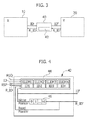
Figure 3 is a schematic illustration of the basic concept of an embodiment; and -
Figure 4 illustrates a specific implementation of an embodiment. - Illustrated in the ensuing description are various specific details aimed at an in-depth understanding of the embodiments. The embodiments can be obtained without one or more of the specific details, or with other methods, components, materials, etc. In other cases, known structures, materials or operations are not illustrated or described in detail so that the various aspects of the embodiments will not be obscured.
- The reference to "an embodiment" or "one embodiment" in the framework of the present description is intended to indicate that a particular configuration, structure, or characteristic described in relation to the embodiment is comprised in at least one embodiment. Hence, phrases such as "in an embodiment" or "in one embodiment", which may be present in different points of this description do not necessarily refer to one and the same embodiment. Furthermore, particular conformations, structures or characteristics can be combined in any adequate way in one or more embodiments.
- The reference numbers used herein are provided merely for reasons of convenience and hence do not define the sphere of protection or the scope of the embodiments.
- The context to which the embodiments considered herein refer is substantially the same as the one already examined with reference to
Figure 1 , i.e., the possible interconnection, for example within a System-on-Chip (SoC), between a first circuit module orisland 10, operating with a protocol X, and a second circuit module orisland 20, operating with a protocol Y, implemented via amodule 40 set between themodules circuit 42 having the characteristics described more fully in what follows with reference toFigure 4 . - Parts and elements that are the same or equivalent to parts and elements already considered previously will hence not be presented and described again.
- In the example of embodiment considered in
Figure 3 , themodule 40 receives at input the signal ID generated in the island 10 (protocol X) and generates as output a new signal ID', different from the input signal, obtained via a mapping operation described more fully in what follows. Any communication protocol (i.e., whatever the protocol Y of the island 20) ensures that the signal R_ID' returned by theisland 20 in response to the signal ID' can be a replica of ID'. The information conveyed by the signal R_ID' can be used for selecting from aqueue 44 the queue element in which the original information is available, without the need to perform a search operation. - The
queue 44 is basically similar to thequeue 32 already described previously: each position or location of thequeue 44 hence comprises two fields, designated by ELEM and ID, respectively. The first field (ELEM1, ELEM2, ..., ELEMn, where n is the "depth" of the queue) is used for storing the information regarding the transaction, whilst the second field (ID1, ID2, ..., IDn) is used as a key and contains a transaction identifier. Once again, the number n of elements comprised in thequeue 44 identifies the maximum number of transactions that are likely to be pending at a given instant of time. - The
module 40 is designed to function as bridge between the module or island 10 (protocol X) and the module or island 20 (protocol Y) by operating in the following way: - when a new transaction is received from the
island 10, the corresponding ID is written in thequeue 42 together with the information to be stored; - the transaction is then treated so that it is suitable for being managed by the protocol Y of the
island 20 and sent at output by mapping on the signal ID' the information regarding the location of thequeue 44 used for said purpose; - when then there arrives from the
island 20 as response a response transaction, the corresponding signal R_ID' is used for identifying (without having to perform any search) the correct memory location and reading therein both the corresponding ID and the original information that has been stored therein; the response transaction can thus be reconstructed on the basis of the protocol X and sent at output to theisland 10. - Operating in this way, the island 20 (i.e., a slave or destination of a communication) in practice sees the island 10 (i.e., a master or initiato of a communication) as a normal module IP that generates a certain number of IDs, which enables masking of the complexity of the
island 10 and simplification of the structure of theisland 20. - As regards the fact that the transaction is "treated" so that it is suitable for being managed by the protocol Y of the island 20 (and sent at output by mapping on the signal ID' the information regarding the location of the
queue 44 used for said purpose), reference may be made, of course without this implying any limit, to the example of the "user-defined" signals of the protocol AXI (de-facto standard): given that it is necessary to integrate two islands that are incompatible in terms of size or for the very presence of said signals, various embodiments as exemplified herein enable solution of the problem in a simple way. - As illustrated in
Figure 4 , in various embodiments thequeue 44 can be managed via read pointers and write pointers, for example resorting to a queue of the pointers designated by 46. Management of the control of the flows can be carried out with any known mechanism. - In various embodiments, the
queue 46 of the pointers can be a FIFO (First-In First-Out) queue. Thequeue 46 can be used for storing the write pointers available and is initialized (reset conditions) with values of from 0 to n-1, where n is the depth of thequeue 44. - The organization as FIFO queue enables handling of the OOO condition in a simple way. The write pointer to be used for writing the information on the current transaction can be derived from the head of the FIFO queue. When there is a return response, since on location of the queue will be empty, the value R_ID' is used as read pointer and at the same time written in the queue of the pointers. In this way, the corresponding location of the
queue 44 can be re-used as soon as it is necessary to write information associated to a new request transaction. - In various embodiments, the function of mapping recalled more than once previously, aimed at mapping on the transaction identifiers information for management of the queue, may involve mapping of the write pointer on ID'.
- Even though, in general, ID' could have a larger number of bits, in various embodiments it is possible to use only the log2n least significant bits (LSBs). Likewise, it is possible to use the log2n least significant bits (LSBs) of R_ID' as read pointer (which can be a copy of ID').
- On the signal R_ID, the original identifier derived from the
queue 44 can be mapped. - The mechanism described guarantees that, in a way independent of the order of the responses, the queue of the pointers contains at each moment the pointers associated to all the empty queue locations.
- Comparing the architecture of a CAM type of
Figure 2 with the architecture represented inFigure 4 , it is evident that various embodiments reduce considerably the circuit complexity and enable any search mechanism to be avoided. - As mentioned in the foregoing, various transaction architectures may employ information identifying the source (e.g., master ID) and transaction IDs. Potential interfacing problems between two domains may arise from possible ID conflicts and from differing ID bit lengths.
- Accordingly, transfer requests from the first IP domain may be translated into request having temporary master IDs and temporary transaction IDs for use in the second IP domain wherein the temporary IDs are then translated back to the original ID when requested data or an acknowledgement is provided to the first IP domain.
- For example, in various embodiments, the original IDs for pending transactions may be stored within a queue and employ the position within the queue along with the original ID to produce a unique ID. Encoded within the unique ID may also be information that specifies the queue location such that the original ID can be accessed by simple addressing.
- However, there are a number of buses where there may exist potential ID conflicts. For example, such ID conflicts may occur if the IP blocks interfaced through the
bridge 42 comprise more than one master, because in this case, the bridge should prevent to use translated IDs which match the IDs of a local master. - Accordingly, in order to avoid such ID conflicts, the
bridge 42 may comprise an additional module or circuit configured to distinguish between master requests and slave responses such that only outgoing master requests and returned slave responses are stored in a queue and translated, i.e., incoming master requests and outgoing slave responses may not be translated. - Moreover, in order to avoid potential ID conflicts, an additional ID prefixing mechanism may be used, such as the ID prefixing provided in AMBA AXI interconnect.
- Accordingly, the
bridge 42 could only provide one unique translated master ID with other outgoing master IDs incorporated into translated transaction IDs, wherein the number of transaction IDs is only limited by the depth of the queue. - Moreover, an additional module or circuit may be provided in order to manage out-of-order transactions. Out-of-order transactions may occur when responses do not occur in the order of requests. In this case a simple circular buffer may not be sufficient but a more complex memory management could be required to keep track of used and free locations.
- Of course, without prejudice to the principle of the invention, the details of implementation and the embodiments may vary, even significantly, with respect to what has been illustrated herein purely by way of non-limiting example, without thereby departing from the scope of the invention as defined by the annexed claims.
- In this regard, it is once again recalled that, as used herein, the expression "different protocols" also comprises the case of different profiles or versions of what formally can be one and the same protocol, whilst various embodiments envisage in general effecting request/response transactions between a first circuit module and a second circuit module operating with different protocols or incompatible interfaces.
Claims (11)
- A method of effecting request/response transactions (REQ/RSP) between a first (10) and a second (20) circuit module, the method comprising providing a queue (44) of memory locations and storing in said memory locations transaction information items (ELEM1, ..., ELEMn) as well as transaction identifiers (ID1,..., IDn) coupled to said transactions,
the method characterized by transmitting between said first (10) and second (20) modules said transaction identifiers (ID', R_ID'), said transaction identifiers having mapped thereon managing information for said queue (44) to reconstruct a response transaction by addressing the location in the queue (44) having stored therein the corresponding request transaction. - The method of claim 1, comprising:- effecting said transactions (REQ/RSP) as read/write operations of the locations in said queue (44) performed by means of pointers, and- mapping onto said transaction identifiers (ID', R_ID') managing information for said queue (44) in the form of pointers to respective memory locations in the queue (44).
- The method of claim 1 or claim 2, comprising:- writing in a location of said queue (44) a request transaction received from said first module (10) along with a corresponding transaction identifier (ID),- adapting said request transaction to said second module (20), and- sending towards said second module (20) said adapted request transaction having coupled a request transaction identifier (ID') modified by mapping thereon managing information identifying the location in said queue where the adapted request transaction is written.
- The method of claim 3, comprising:- receiving from said second module (20), in response to said adapted request transaction sent towards the second module (20), a response transaction having coupled a respective response transaction identifier (R_ID'),- identifying, based on said respective response transaction identifier (R_ID'), the location in said queue where said request transaction is written, and- reconstructing said response transaction in a form compatible with said first module (10), and- sending the reconstructed response transaction to said first module (10).
- The method of claim 4, wherein said respective response transaction identifier (R_ID') is a replica of said corresponding request transaction identifier (ID') as modified.
- The method of any of the previous claims, wherein said managing information for the queue includes at least one of:- a write pointer mapped onto a request transaction identifier (ID'), and- a read pointer mapped onto a response transaction identifier (R_ID').
- The method of any of the previous claims,comprising:- providing a queue of pointers (46),- taking from said pointer queue (46) a write pointer to write in a location (44) of said queue a request transaction received from said first module (10), and- inputting to said pointer queue (46) a read pointer used for a response transaction received from said second module (20), thereby permitting the corresponding location (44) in the queue to be re-used to write a subsequent request transaction received from said first module (10).
- The method of claim 7, comprising providing said pointer queue (46) as a FIFO (First-in First-out) queue and taking said write pointer from the head of said queue.
- A device for implementing the method of any of the previous claims, comprising:- a memory (44) interposed between said first (10) and second (20) module including memory locations with a first field (ELEM1, ..., ELEMn) to store said transaction information items as well as a second field (ID1.....,IDn) to store said transaction identifiers coupled therewith,- a pointer memory (46) to store at least part of a set of pointers for mapping mapped onto said transaction identifiers,
the device configured for mapping onto said transaction identifiers (ID', R_ID') managing information for said queue (44) in the form of pointers to respective memory locations in the queue (44). - The device of claim 9, the device being interposed between said first (10) and second (20) module with respective transmission lines for signals (ID, R_ID, ID', R_ID') conveying said transaction identifiers.
- The device of claim 10, wherein said device and said first (10) and said second (20) module are jointly integrated in a System-on-Chip.
Applications Claiming Priority (1)
| Application Number | Priority Date | Filing Date | Title |
|---|---|---|---|
| ITTO20100420 | 2010-05-20 |
Publications (2)
| Publication Number | Publication Date |
|---|---|
| EP2388707A1 true EP2388707A1 (en) | 2011-11-23 |
| EP2388707B1 EP2388707B1 (en) | 2014-03-26 |
Family
ID=43242597
Family Applications (1)
| Application Number | Title | Priority Date | Filing Date |
|---|---|---|---|
| EP11166340.7A Not-in-force EP2388707B1 (en) | 2010-05-20 | 2011-05-17 | Interconnection method and device, for example for systems-on-chip |
Country Status (2)
| Country | Link |
|---|---|
| US (1) | US8631184B2 (en) |
| EP (1) | EP2388707B1 (en) |
Cited By (1)
| Publication number | Priority date | Publication date | Assignee | Title |
|---|---|---|---|---|
| WO2014039572A1 (en) * | 2012-09-06 | 2014-03-13 | Apple Inc. | Low power, area-efficient tracking buffer |
Families Citing this family (12)
| Publication number | Priority date | Publication date | Assignee | Title |
|---|---|---|---|---|
| KR101699781B1 (en) * | 2010-10-19 | 2017-01-26 | 삼성전자주식회사 | System-on-chip and data arbitration method thereof |
| US8533377B2 (en) * | 2011-05-28 | 2013-09-10 | Lsi Corporation | System and method for allocating transaction ID in a system with a plurality of processing modules |
| US8504756B2 (en) * | 2011-05-30 | 2013-08-06 | Lsi Corporation | System, circuit and method for improving system-on-chip bandwidth performance for high latency peripheral read accesses |
| US9489304B1 (en) * | 2011-11-14 | 2016-11-08 | Marvell International Ltd. | Bi-domain bridge enhanced systems and communication methods |
| US20130159591A1 (en) * | 2011-12-14 | 2013-06-20 | International Business Machines Corporation | Verifying data received out-of-order from a bus |
| US8929376B2 (en) * | 2012-02-17 | 2015-01-06 | Netronome Systems, Incorporated | Flow control using a local event ring in an island-based network flow processor |
| US9069649B2 (en) * | 2012-02-17 | 2015-06-30 | Netronome Systems, Incorporated | Distributed credit FIFO link of a configurable mesh data bus |
| US9348775B2 (en) * | 2012-03-16 | 2016-05-24 | Analog Devices, Inc. | Out-of-order execution of bus transactions |
| US8902902B2 (en) | 2012-07-18 | 2014-12-02 | Netronome Systems, Incorporated | Recursive lookup with a hardware trie structure that has no sequential logic elements |
| JP6144348B2 (en) * | 2012-09-25 | 2017-06-07 | クゥアルコム・テクノロジーズ・インコーポレイテッド | Network over chip socket protocol |
| US9471538B2 (en) * | 2012-09-25 | 2016-10-18 | Qualcomm Technologies, Inc. | Network on a chip socket protocol |
| US12045178B2 (en) * | 2022-02-10 | 2024-07-23 | Mellanox Technologies, Ltd. | Devices, methods, and systems for disaggregated memory resources in a computing environment |
Citations (3)
| Publication number | Priority date | Publication date | Assignee | Title |
|---|---|---|---|---|
| US20020083256A1 (en) * | 2000-08-31 | 2002-06-27 | Pannell Roger D. | System and method for increasing the count of outstanding split transactions |
| US20040024947A1 (en) * | 2002-07-31 | 2004-02-05 | Frank Barth | Buffering non-posted read commands and responses |
| US20060190655A1 (en) * | 2005-02-24 | 2006-08-24 | International Business Machines Corporation | Apparatus and method for transaction tag mapping between bus domains |
Family Cites Families (9)
| Publication number | Priority date | Publication date | Assignee | Title |
|---|---|---|---|---|
| US6195722B1 (en) * | 1998-01-26 | 2001-02-27 | Intel Corporation | Method and apparatus for deferring transactions on a host bus having a third party agent |
| US6493800B1 (en) * | 1999-03-31 | 2002-12-10 | International Business Machines Corporation | Method and system for dynamically partitioning a shared cache |
| US6317806B1 (en) * | 1999-05-20 | 2001-11-13 | International Business Machines Corporation | Static queue and index queue for storing values identifying static queue locations |
| US6996559B1 (en) * | 1999-12-23 | 2006-02-07 | Nortel Networks Limited | IP address resolution methods and apparatus |
| US6449701B1 (en) * | 2000-09-20 | 2002-09-10 | Broadcom Corporation | Out of order associative queue in two clock domains |
| US7373444B2 (en) * | 2005-04-15 | 2008-05-13 | Kabushiki Kaisha Toshiba | Systems and methods for manipulating entries in a command buffer using tag information |
| US7685350B2 (en) * | 2005-06-24 | 2010-03-23 | Intel Corporation | Remote node index mapping mechanism for serial attached storage devices |
| US7398361B2 (en) * | 2005-08-30 | 2008-07-08 | P.A. Semi, Inc. | Combined buffer for snoop, store merging, load miss, and writeback operations |
| JP4357473B2 (en) * | 2005-11-04 | 2009-11-04 | 株式会社ソニー・コンピュータエンタテインメント | Data processing system and program |
-
2011
- 2011-05-17 EP EP11166340.7A patent/EP2388707B1/en not_active Not-in-force
- 2011-05-20 US US13/112,802 patent/US8631184B2/en not_active Expired - Fee Related
Patent Citations (3)
| Publication number | Priority date | Publication date | Assignee | Title |
|---|---|---|---|---|
| US20020083256A1 (en) * | 2000-08-31 | 2002-06-27 | Pannell Roger D. | System and method for increasing the count of outstanding split transactions |
| US20040024947A1 (en) * | 2002-07-31 | 2004-02-05 | Frank Barth | Buffering non-posted read commands and responses |
| US20060190655A1 (en) * | 2005-02-24 | 2006-08-24 | International Business Machines Corporation | Apparatus and method for transaction tag mapping between bus domains |
Cited By (2)
| Publication number | Priority date | Publication date | Assignee | Title |
|---|---|---|---|---|
| WO2014039572A1 (en) * | 2012-09-06 | 2014-03-13 | Apple Inc. | Low power, area-efficient tracking buffer |
| US9201829B2 (en) | 2012-09-06 | 2015-12-01 | Apple Inc. | Low power, area-efficient tracking buffer |
Also Published As
| Publication number | Publication date |
|---|---|
| US20110289253A1 (en) | 2011-11-24 |
| EP2388707B1 (en) | 2014-03-26 |
| US8631184B2 (en) | 2014-01-14 |
Similar Documents
| Publication | Publication Date | Title |
|---|---|---|
| EP2388707B1 (en) | Interconnection method and device, for example for systems-on-chip | |
| US20240394203A1 (en) | Interconnect apparatus for bus | |
| US7320041B2 (en) | Controlling flow of data between data processing systems via a memory | |
| KR100555394B1 (en) | Method and Mechanism for Remote Key Verification for NVIO / IENFIENAIDN Applications | |
| US7409468B2 (en) | Controlling flow of data between data processing systems via a memory | |
| US7606933B2 (en) | Shared memory and high performance communication using interconnect tunneling | |
| CN110557311B (en) | Inter-processor communication method for inter-die access latency in system-in-package | |
| US20120079154A1 (en) | Transaction reordering arrangement | |
| JP2004520646A (en) | Method and apparatus for transferring an interrupt from a peripheral device to a host computer system | |
| CN116561036B (en) | Data access control methods, devices, equipment and storage media | |
| CN116489177A (en) | A block-storage-based IO access method, device, electronic device, and medium | |
| WO2014203036A1 (en) | Method and apparatus for offloading functional data from an interconnect component | |
| US10185684B2 (en) | System interconnect and operating method of system interconnect | |
| US6425071B1 (en) | Subsystem bridge of AMBA's ASB bus to peripheral component interconnect (PCI) bus | |
| GB2396450A (en) | Data bus system and method for performing cross-access between buses | |
| CN108664335A (en) | Method and device for queue communication through proxy | |
| US7822903B2 (en) | Single bus command having transfer information for transferring data in a processing system | |
| US9672168B2 (en) | System interconnection of system-on-chip | |
| Hellwagner | The SCI Standard and Applications of SCI. | |
| US5636370A (en) | System and method for interfacing risc busses to peripheral circuits using another template of busses in a data communication adapter | |
| US6507609B1 (en) | Mechanism for capturing and reporting interrupt events of different clock domains | |
| CN120834969B (en) | A FlexRay communication system based on on-chip shared memory | |
| US20250123981A1 (en) | Communication method performed on network-on-chip | |
| CN120973710A (en) | Data interaction methods and device consistency circuits for computing fast link systems | |
| CN108664333B (en) | Message system of system on chip |
Legal Events
| Date | Code | Title | Description |
|---|---|---|---|
| AK | Designated contracting states |
Kind code of ref document: A1 Designated state(s): AL AT BE BG CH CY CZ DE DK EE ES FI FR GB GR HR HU IE IS IT LI LT LU LV MC MK MT NL NO PL PT RO RS SE SI SK SM TR |
|
| AX | Request for extension of the european patent |
Extension state: BA ME |
|
| PUAI | Public reference made under article 153(3) epc to a published international application that has entered the european phase |
Free format text: ORIGINAL CODE: 0009012 |
|
| 17P | Request for examination filed |
Effective date: 20120328 |
|
| RAP1 | Party data changed (applicant data changed or rights of an application transferred) |
Owner name: STMICROELECTRONICS (GRENOBLE 2) SAS Owner name: STMICROELECTRONICS SRL |
|
| RIC1 | Information provided on ipc code assigned before grant |
Ipc: G06F 13/40 20060101AFI20130809BHEP |
|
| GRAP | Despatch of communication of intention to grant a patent |
Free format text: ORIGINAL CODE: EPIDOSNIGR1 |
|
| INTG | Intention to grant announced |
Effective date: 20131031 |
|
| GRAS | Grant fee paid |
Free format text: ORIGINAL CODE: EPIDOSNIGR3 |
|
| GRAA | (expected) grant |
Free format text: ORIGINAL CODE: 0009210 |
|
| AK | Designated contracting states |
Kind code of ref document: B1 Designated state(s): AL AT BE BG CH CY CZ DE DK EE ES FI FR GB GR HR HU IE IS IT LI LT LU LV MC MK MT NL NO PL PT RO RS SE SI SK SM TR |
|
| REG | Reference to a national code |
Ref country code: GB Ref legal event code: FG4D |
|
| REG | Reference to a national code |
Ref country code: CH Ref legal event code: EP |
|
| REG | Reference to a national code |
Ref country code: AT Ref legal event code: REF Ref document number: 659299 Country of ref document: AT Kind code of ref document: T Effective date: 20140415 |
|
| REG | Reference to a national code |
Ref country code: IE Ref legal event code: FG4D |
|
| REG | Reference to a national code |
Ref country code: DE Ref legal event code: R096 Ref document number: 602011005694 Country of ref document: DE Effective date: 20140508 |
|
| PG25 | Lapsed in a contracting state [announced via postgrant information from national office to epo] |
Ref country code: NO Free format text: LAPSE BECAUSE OF FAILURE TO SUBMIT A TRANSLATION OF THE DESCRIPTION OR TO PAY THE FEE WITHIN THE PRESCRIBED TIME-LIMIT Effective date: 20140626 Ref country code: LT Free format text: LAPSE BECAUSE OF FAILURE TO SUBMIT A TRANSLATION OF THE DESCRIPTION OR TO PAY THE FEE WITHIN THE PRESCRIBED TIME-LIMIT Effective date: 20140326 |
|
| REG | Reference to a national code |
Ref country code: AT Ref legal event code: MK05 Ref document number: 659299 Country of ref document: AT Kind code of ref document: T Effective date: 20140326 |
|
| REG | Reference to a national code |
Ref country code: NL Ref legal event code: VDEP Effective date: 20140326 |
|
| REG | Reference to a national code |
Ref country code: LT Ref legal event code: MG4D |
|
| PG25 | Lapsed in a contracting state [announced via postgrant information from national office to epo] |
Ref country code: SE Free format text: LAPSE BECAUSE OF FAILURE TO SUBMIT A TRANSLATION OF THE DESCRIPTION OR TO PAY THE FEE WITHIN THE PRESCRIBED TIME-LIMIT Effective date: 20140326 Ref country code: FI Free format text: LAPSE BECAUSE OF FAILURE TO SUBMIT A TRANSLATION OF THE DESCRIPTION OR TO PAY THE FEE WITHIN THE PRESCRIBED TIME-LIMIT Effective date: 20140326 |
|
| PG25 | Lapsed in a contracting state [announced via postgrant information from national office to epo] |
Ref country code: LV Free format text: LAPSE BECAUSE OF FAILURE TO SUBMIT A TRANSLATION OF THE DESCRIPTION OR TO PAY THE FEE WITHIN THE PRESCRIBED TIME-LIMIT Effective date: 20140326 Ref country code: HR Free format text: LAPSE BECAUSE OF FAILURE TO SUBMIT A TRANSLATION OF THE DESCRIPTION OR TO PAY THE FEE WITHIN THE PRESCRIBED TIME-LIMIT Effective date: 20140326 Ref country code: RS Free format text: LAPSE BECAUSE OF FAILURE TO SUBMIT A TRANSLATION OF THE DESCRIPTION OR TO PAY THE FEE WITHIN THE PRESCRIBED TIME-LIMIT Effective date: 20140326 |
|
| PG25 | Lapsed in a contracting state [announced via postgrant information from national office to epo] |
Ref country code: CY Free format text: LAPSE BECAUSE OF FAILURE TO SUBMIT A TRANSLATION OF THE DESCRIPTION OR TO PAY THE FEE WITHIN THE PRESCRIBED TIME-LIMIT Effective date: 20140326 Ref country code: RO Free format text: LAPSE BECAUSE OF FAILURE TO SUBMIT A TRANSLATION OF THE DESCRIPTION OR TO PAY THE FEE WITHIN THE PRESCRIBED TIME-LIMIT Effective date: 20140326 Ref country code: IS Free format text: LAPSE BECAUSE OF FAILURE TO SUBMIT A TRANSLATION OF THE DESCRIPTION OR TO PAY THE FEE WITHIN THE PRESCRIBED TIME-LIMIT Effective date: 20140726 Ref country code: CZ Free format text: LAPSE BECAUSE OF FAILURE TO SUBMIT A TRANSLATION OF THE DESCRIPTION OR TO PAY THE FEE WITHIN THE PRESCRIBED TIME-LIMIT Effective date: 20140326 Ref country code: NL Free format text: LAPSE BECAUSE OF FAILURE TO SUBMIT A TRANSLATION OF THE DESCRIPTION OR TO PAY THE FEE WITHIN THE PRESCRIBED TIME-LIMIT Effective date: 20140326 Ref country code: BE Free format text: LAPSE BECAUSE OF FAILURE TO SUBMIT A TRANSLATION OF THE DESCRIPTION OR TO PAY THE FEE WITHIN THE PRESCRIBED TIME-LIMIT Effective date: 20140326 Ref country code: EE Free format text: LAPSE BECAUSE OF FAILURE TO SUBMIT A TRANSLATION OF THE DESCRIPTION OR TO PAY THE FEE WITHIN THE PRESCRIBED TIME-LIMIT Effective date: 20140326 Ref country code: BG Free format text: LAPSE BECAUSE OF FAILURE TO SUBMIT A TRANSLATION OF THE DESCRIPTION OR TO PAY THE FEE WITHIN THE PRESCRIBED TIME-LIMIT Effective date: 20140626 |
|
| PG25 | Lapsed in a contracting state [announced via postgrant information from national office to epo] |
Ref country code: ES Free format text: LAPSE BECAUSE OF FAILURE TO SUBMIT A TRANSLATION OF THE DESCRIPTION OR TO PAY THE FEE WITHIN THE PRESCRIBED TIME-LIMIT Effective date: 20140326 Ref country code: SK Free format text: LAPSE BECAUSE OF FAILURE TO SUBMIT A TRANSLATION OF THE DESCRIPTION OR TO PAY THE FEE WITHIN THE PRESCRIBED TIME-LIMIT Effective date: 20140326 Ref country code: AT Free format text: LAPSE BECAUSE OF FAILURE TO SUBMIT A TRANSLATION OF THE DESCRIPTION OR TO PAY THE FEE WITHIN THE PRESCRIBED TIME-LIMIT Effective date: 20140326 Ref country code: PL Free format text: LAPSE BECAUSE OF FAILURE TO SUBMIT A TRANSLATION OF THE DESCRIPTION OR TO PAY THE FEE WITHIN THE PRESCRIBED TIME-LIMIT Effective date: 20140326 |
|
| PG25 | Lapsed in a contracting state [announced via postgrant information from national office to epo] |
Ref country code: PT Free format text: LAPSE BECAUSE OF FAILURE TO SUBMIT A TRANSLATION OF THE DESCRIPTION OR TO PAY THE FEE WITHIN THE PRESCRIBED TIME-LIMIT Effective date: 20140728 Ref country code: LU Free format text: LAPSE BECAUSE OF FAILURE TO SUBMIT A TRANSLATION OF THE DESCRIPTION OR TO PAY THE FEE WITHIN THE PRESCRIBED TIME-LIMIT Effective date: 20140517 |
|
| REG | Reference to a national code |
Ref country code: CH Ref legal event code: PL |
|
| REG | Reference to a national code |
Ref country code: DE Ref legal event code: R097 Ref document number: 602011005694 Country of ref document: DE |
|
| PG25 | Lapsed in a contracting state [announced via postgrant information from national office to epo] |
Ref country code: CH Free format text: LAPSE BECAUSE OF NON-PAYMENT OF DUE FEES Effective date: 20140531 Ref country code: MC Free format text: LAPSE BECAUSE OF FAILURE TO SUBMIT A TRANSLATION OF THE DESCRIPTION OR TO PAY THE FEE WITHIN THE PRESCRIBED TIME-LIMIT Effective date: 20140326 Ref country code: LI Free format text: LAPSE BECAUSE OF NON-PAYMENT OF DUE FEES Effective date: 20140531 Ref country code: DK Free format text: LAPSE BECAUSE OF FAILURE TO SUBMIT A TRANSLATION OF THE DESCRIPTION OR TO PAY THE FEE WITHIN THE PRESCRIBED TIME-LIMIT Effective date: 20140326 |
|
| PLBE | No opposition filed within time limit |
Free format text: ORIGINAL CODE: 0009261 |
|
| STAA | Information on the status of an ep patent application or granted ep patent |
Free format text: STATUS: NO OPPOSITION FILED WITHIN TIME LIMIT |
|
| REG | Reference to a national code |
Ref country code: IE Ref legal event code: MM4A |
|
| 26N | No opposition filed |
Effective date: 20150106 |
|
| PG25 | Lapsed in a contracting state [announced via postgrant information from national office to epo] |
Ref country code: IT Free format text: LAPSE BECAUSE OF FAILURE TO SUBMIT A TRANSLATION OF THE DESCRIPTION OR TO PAY THE FEE WITHIN THE PRESCRIBED TIME-LIMIT Effective date: 20140326 |
|
| REG | Reference to a national code |
Ref country code: DE Ref legal event code: R097 Ref document number: 602011005694 Country of ref document: DE Effective date: 20150106 |
|
| PG25 | Lapsed in a contracting state [announced via postgrant information from national office to epo] |
Ref country code: IE Free format text: LAPSE BECAUSE OF NON-PAYMENT OF DUE FEES Effective date: 20140517 |
|
| PG25 | Lapsed in a contracting state [announced via postgrant information from national office to epo] |
Ref country code: SI Free format text: LAPSE BECAUSE OF FAILURE TO SUBMIT A TRANSLATION OF THE DESCRIPTION OR TO PAY THE FEE WITHIN THE PRESCRIBED TIME-LIMIT Effective date: 20140326 |
|
| GBPC | Gb: european patent ceased through non-payment of renewal fee |
Effective date: 20150517 |
|
| PG25 | Lapsed in a contracting state [announced via postgrant information from national office to epo] |
Ref country code: MT Free format text: LAPSE BECAUSE OF FAILURE TO SUBMIT A TRANSLATION OF THE DESCRIPTION OR TO PAY THE FEE WITHIN THE PRESCRIBED TIME-LIMIT Effective date: 20140326 |
|
| REG | Reference to a national code |
Ref country code: FR Ref legal event code: PLFP Year of fee payment: 6 |
|
| PG25 | Lapsed in a contracting state [announced via postgrant information from national office to epo] |
Ref country code: SM Free format text: LAPSE BECAUSE OF FAILURE TO SUBMIT A TRANSLATION OF THE DESCRIPTION OR TO PAY THE FEE WITHIN THE PRESCRIBED TIME-LIMIT Effective date: 20140326 Ref country code: GB Free format text: LAPSE BECAUSE OF NON-PAYMENT OF DUE FEES Effective date: 20150517 |
|
| PG25 | Lapsed in a contracting state [announced via postgrant information from national office to epo] |
Ref country code: GR Free format text: LAPSE BECAUSE OF FAILURE TO SUBMIT A TRANSLATION OF THE DESCRIPTION OR TO PAY THE FEE WITHIN THE PRESCRIBED TIME-LIMIT Effective date: 20140627 |
|
| PG25 | Lapsed in a contracting state [announced via postgrant information from national office to epo] |
Ref country code: TR Free format text: LAPSE BECAUSE OF FAILURE TO SUBMIT A TRANSLATION OF THE DESCRIPTION OR TO PAY THE FEE WITHIN THE PRESCRIBED TIME-LIMIT Effective date: 20140326 Ref country code: HU Free format text: LAPSE BECAUSE OF FAILURE TO SUBMIT A TRANSLATION OF THE DESCRIPTION OR TO PAY THE FEE WITHIN THE PRESCRIBED TIME-LIMIT; INVALID AB INITIO Effective date: 20110517 |
|
| REG | Reference to a national code |
Ref country code: FR Ref legal event code: PLFP Year of fee payment: 7 |
|
| REG | Reference to a national code |
Ref country code: FR Ref legal event code: PLFP Year of fee payment: 8 |
|
| PG25 | Lapsed in a contracting state [announced via postgrant information from national office to epo] |
Ref country code: MK Free format text: LAPSE BECAUSE OF FAILURE TO SUBMIT A TRANSLATION OF THE DESCRIPTION OR TO PAY THE FEE WITHIN THE PRESCRIBED TIME-LIMIT Effective date: 20140326 |
|
| PG25 | Lapsed in a contracting state [announced via postgrant information from national office to epo] |
Ref country code: AL Free format text: LAPSE BECAUSE OF FAILURE TO SUBMIT A TRANSLATION OF THE DESCRIPTION OR TO PAY THE FEE WITHIN THE PRESCRIBED TIME-LIMIT Effective date: 20140326 |
|
| PGFP | Annual fee paid to national office [announced via postgrant information from national office to epo] |
Ref country code: DE Payment date: 20190418 Year of fee payment: 9 |
|
| PGFP | Annual fee paid to national office [announced via postgrant information from national office to epo] |
Ref country code: FR Payment date: 20190418 Year of fee payment: 9 |
|
| REG | Reference to a national code |
Ref country code: DE Ref legal event code: R119 Ref document number: 602011005694 Country of ref document: DE |
|
| PG25 | Lapsed in a contracting state [announced via postgrant information from national office to epo] |
Ref country code: FR Free format text: LAPSE BECAUSE OF NON-PAYMENT OF DUE FEES Effective date: 20200531 |
|
| PG25 | Lapsed in a contracting state [announced via postgrant information from national office to epo] |
Ref country code: DE Free format text: LAPSE BECAUSE OF NON-PAYMENT OF DUE FEES Effective date: 20201201 |