EP2387236A1 - Receiving device and manufacturing method thereof - Google Patents
Receiving device and manufacturing method thereof Download PDFInfo
- Publication number
- EP2387236A1 EP2387236A1 EP11164452A EP11164452A EP2387236A1 EP 2387236 A1 EP2387236 A1 EP 2387236A1 EP 11164452 A EP11164452 A EP 11164452A EP 11164452 A EP11164452 A EP 11164452A EP 2387236 A1 EP2387236 A1 EP 2387236A1
- Authority
- EP
- European Patent Office
- Prior art keywords
- board
- conductive
- receiving device
- digital
- lid
- Prior art date
- Legal status (The legal status is an assumption and is not a legal conclusion. Google has not performed a legal analysis and makes no representation as to the accuracy of the status listed.)
- Withdrawn
Links
- 238000004519 manufacturing process Methods 0.000 title claims description 7
- 230000003068 static effect Effects 0.000 description 17
- 238000003780 insertion Methods 0.000 description 16
- 230000037431 insertion Effects 0.000 description 16
- 230000002093 peripheral effect Effects 0.000 description 7
- 239000002184 metal Substances 0.000 description 6
- 229910052751 metal Inorganic materials 0.000 description 6
- 238000000034 method Methods 0.000 description 4
- 230000008901 benefit Effects 0.000 description 3
- 230000007547 defect Effects 0.000 description 2
- 238000005530 etching Methods 0.000 description 2
- 230000006870 function Effects 0.000 description 2
- 239000012811 non-conductive material Substances 0.000 description 2
- 230000005236 sound signal Effects 0.000 description 2
- RYGMFSIKBFXOCR-UHFFFAOYSA-N Copper Chemical compound [Cu] RYGMFSIKBFXOCR-UHFFFAOYSA-N 0.000 description 1
- 230000004075 alteration Effects 0.000 description 1
- 230000008859 change Effects 0.000 description 1
- 238000006243 chemical reaction Methods 0.000 description 1
- 239000002131 composite material Substances 0.000 description 1
- 239000011889 copper foil Substances 0.000 description 1
- 230000010354 integration Effects 0.000 description 1
- 230000008520 organization Effects 0.000 description 1
- 239000011347 resin Substances 0.000 description 1
- 229920005989 resin Polymers 0.000 description 1
- 238000006467 substitution reaction Methods 0.000 description 1
- 239000000758 substrate Substances 0.000 description 1
Images




Classifications
-
- H—ELECTRICITY
- H04—ELECTRIC COMMUNICATION TECHNIQUE
- H04N—PICTORIAL COMMUNICATION, e.g. TELEVISION
- H04N5/00—Details of television systems
- H04N5/64—Constructional details of receivers, e.g. cabinets or dust covers
-
- Y—GENERAL TAGGING OF NEW TECHNOLOGICAL DEVELOPMENTS; GENERAL TAGGING OF CROSS-SECTIONAL TECHNOLOGIES SPANNING OVER SEVERAL SECTIONS OF THE IPC; TECHNICAL SUBJECTS COVERED BY FORMER USPC CROSS-REFERENCE ART COLLECTIONS [XRACs] AND DIGESTS
- Y10—TECHNICAL SUBJECTS COVERED BY FORMER USPC
- Y10T—TECHNICAL SUBJECTS COVERED BY FORMER US CLASSIFICATION
- Y10T29/00—Metal working
- Y10T29/49—Method of mechanical manufacture
- Y10T29/49002—Electrical device making
- Y10T29/49117—Conductor or circuit manufacturing
- Y10T29/49124—On flat or curved insulated base, e.g., printed circuit, etc.
- Y10T29/49147—Assembling terminal to base
Definitions
- the present invention generally relates to a receiving device including a board in which components for receiving digital broadcasting signals are installed.
- a broadcasting method for television broadcasting is changing from an analog method to a digital method.
- a receiving device which receives a broadcast signal of the digital method such as a digitized terrestrial broadcast and converts the broadcast signal to a signal which can be heard and viewed is a commercial reality.
- Patent Document 1 discloses an electronic device including a metal cover 117, a chassis 115, a power board 112 and a signal processing board 113 both of which boards are accommodated between the metal cover 117 and the chassis 115.
- Patent Document 1 Japanese Laid-open Patent Publication No. 2007-324858
- the metal cover and the chassis which are made of a conductive metal.
- the conductive metal used for the cover and the chassis may be changed to a non-conductive material.
- embodiments of the present invention may provide a novel and useful receiving device solving one or more of the problems discussed above by protecting integrated components from static charge even though a casing (e.g. cover and chassis) is non-conductive.
- a casing e.g. cover and chassis
- the embodiments of the present invention may provide a receiving device including a board on which components for receiving a digital broadcasting signal are mounted; a non-conductive casing configured to accommodate the board; and a non-conductive lid configured to cover the board and being connected to the non-conductive casing, wherein the board has a conductive portion located in an edge portion of the board facing a gap formed in a connecting portion between the casing and the lid.
- FIG. 6 is a cross-sectional view of an example receiving device.
- the above receiving device 10 functions for receiving the digital broadcasting signal.
- the receiving device 10 includes a body 12 and a lid 13.
- An analog board 14 and a digital board 50 illustrated in FIG. 7 are accommodated in the body 12 (the digital board 50 is omitted in FIG. 6 ).
- a card insertion port 15 is formed in the body 12.
- the analog board 14 includes a power supply circuit 16, a connector 17, a tuner 18 and a guide member 19 for guiding the contact-type IC card 11 to the connector 17.
- the length W of the guide member 19 is designed so as to accommodate the entire contact-type IC card 11 into the body 12 when the contact-type IC card 11 is inserted into the connector 17.
- the guide member 19 is installed on the analog board 14 so that a card insertion slit 21 is arranged in the card insertion port 15.
- the body 12 accommodating the digital board 50 ( FIG. 7 ) between the connector 17 and the lid 13 is formed of a conductive metal.
- FIG. 1 is an exploded perspective view of a receiving device 100 of the Embodiment.
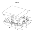
- FIG. 2 is another exploded perspective view of the receiving device 100 of the Embodiment. Referring to FIG. 2 , a digital board 140 is omitted.
- the receiving device 100 of the Embodiment may be a set top box which receives a digital broadcasting signal or a digital tuner.
- a contact-type integrated circuit (IC) called B-CAS card 20 is inserted in the receiving device 100, the receiving device can perform a receiving function.
- An IC chip (not illustrated) is installed in the B-CAS card 20.
- An identification number and an encryption key are unique to the B-CAS card 20 and stored in the IC chip of the B-CAS card.
- the receiving device 100 includes a casing body 110 and a lid 120.
- a power board 130 and the digital board 140 are accommodate in the casing body 110.
- the casing body 110 has an insertion hole 111 through which the B-CAS card 20 is inserted.
- the B-CAS card 20 is inserted into the insertion hole and connected to a B-CAS card connector 150.
- the power board 130 includes a power supply circuit formed mainly of an analog circuit and the B-CAS card connector 150.
- the digital board 140 of the Embodiment is a double-surface mount substrate and has various digital circuits such as a central processing unit (CPU) and a memory chip as illustrated FIG. 4 to be described below.
- CPU central processing unit
- a memory chip as illustrated FIG. 4 to be described below.
- a tuner 160 is mounted for receiving the digital broadcasting signal. Pins 141 are for the tuner 160.
- the digital broadcasting signal is input in the tuner 160 via an antenna or a cable line connected to the receiving device 100.
- a frequency conversion unit of the tuner 160 converts the digital broadcasting signal to an intermediate frequency signal (IF signal) including an intermediate frequency corresponding to a signal component of a desired channel to be watched or heard.
- IF signal intermediate frequency signal
- the channel for the tuner 160 is designated based on selection channel information input from a user input device (not illustrated) such as a remote controller and a touch panel display with which the user can select the channel to be received.
- a user input device not illustrated
- the tuner 160 tunes the frequency corresponding to the selected channel.
- electronic components mounted on the digital board 140 may be a decoder IC and a power supply circuit which supplies a constant direct current voltage to the electronic components mounted on the digital board 140 such as the tuner 160 and the decoder IC.
- the decoder IC is an integrated circuit converting an IF signal tuned by the tuner 160 to an analog composite image signal and an analog audio signal. These image and audio signals are output from RCA terminals 43 through 45 mounted on the digital board 140.
- the receiving device 100 of the Embodiment includes the tuner 160 between the insertion hole 111 of the casing body 110 and a card insertion port 151 of the B-CAS card connector 150.
- the length W1 between the insertion hole 111 of the casing body 110 and the card insertion port 151 of the B-CAS card connector 150 is designed so that the entire B-CAS card 20 is accommodated in the casing body 110 when the B-CAS card 20 is inserted into the B-CAS card connector 150.
- the tuner 160 is arranged in a space between the insertion hole 111 of the casing body 110 and the card insertion port 151 of the B-CAS card connector 150.
- the receiving device 100 can be made small.
- FIG. 3 is a cross-sectional view of the receiving device 100 illustrated in FIG. 1 taken along a line A-A.
- FIG. 3 illustrates a state where the B-CAS card 20 is inserted into the receiving device 100.
- the tuner 160 is arranged so as not to contact the B-CAS card 20 when the B-CAS card 20 is inserted into the B-CAS card connector 150.
- the tuner 160 is arranged so as not to overlap the insertion hole 111 and the card insertion port 151 in the direction of inserting the B-CAS card 20.
- the B-CAS card 20 can be inserted into the B-CAS card connector 150 without being interrupted from insertion into the B-CAS card connector 150.
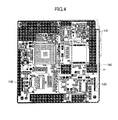
- FIG. 4 illustrates an example of a board layout of the digital board 140 on the side of the lid 120.
- the tuner 160 is mounted on a second surface opposite to a first surface (the surface on the side of the lid 120) illustrated in FIG. 1 .
- the tuner 160 is arranged so that the side having more pins than the other side is positioned in the vicinity of and inside an edge of the digital board 140.
- Through holes 144 are formed to cause the pins of the tuner 160 to penetrate through the digital board 140 in the vicinity of and inside the edge of the digital board 140.
- the tuner 160 is surface mounted on the digital board 140 by inserting the pins 141 into the through holes 144.
- the IC connected to many signal lines can be surface-mounted on an area H (see FIG. 4 ) on a back side of an area in which the tuner 160 is surface-mounted thereby achieving high integration of the digital board 140.
- the tuner 160 is mounted on the digital board 140.
- Image signal lines in the vicinity of the tuner 160 may be connected to the digital board 140 and noise in the image signal can be reduced. Further, it is possible to reduce the number of the signal lines connecting the power board 130 to the digital board 140. Therefore, the number of pins of the connector connecting the power board 130 to the digital board 140 can be made small.
- a port for a debug circuit is provided on the edge of the digital board 140 of the Embodiment.
- the digital board 140 can be made small or miniaturized.
- the ports 145 and 146 for connecting to the debug circuit are located on the digital board 140.
- the ports for the debug circuit 145 and 146 are formed inside regions where components are prevented from being located on both ends of the digital board 140.
- the regions where components are prevented from being located on the both ends of the digital board 140 are provided for supporting the digital board 140 in a manufacturing process of the digital board 140. It is prohibited to mount the components on the regions.
- the number of the ports 145 and 146 for the debug circuits is the same as the number of the signals necessary for debugging the IC mounted on the digital board 140. Therefore, the numbers of the ports 145 and 146 for the debug circuit become relatively smaller than the number of pins for an ordinarily used debug connector.
- a debugging circuit is inserted into the digital board 140 to thereby debug the digital board 140.
- the debugging is performed for each digital board 140 after mass-producing the digital boards 140. Therefore, when there is a defect in the product, it is possible to check for the defect in each digital board 140 as products.
- the digital board 140 on which the electronic components are mounted is accommodated and covered by the casing body 110 and the lid 120.
- the casing body 110 is non-conductive.
- the lid 120 is also non-conductive.
- the non-conductive material may be a resin.
- a connection end 112 of the casing body 110 for connecting the lid 120 and a connection end 121 of the lid 120 for connecting the casing body 110 are not melted and joined. Therefore, a small gap 210 may be formed to allow intrusion of static charge from the outside of the receiving device 100.
- the gap 210 is especially prone to be formed when the lid 120 is attached to the casing body 110 with an attaching member such as a snap fit or a screw.
- plural conductive patterns 201 through 206 are formed to face the gap 210 in a board peripheral portion 147 interposed between the mounted portion of the electronic components and a board end 143 of the digital board 140.
- the mounted portion of the electronic components is a land or a through hole formed on the digital board 140 in order to mount the electronic components.
- the conductive patterns 201 through 206 are formed on a board surface on one side opposite to the gap 210, i.e., the lower surface of the digital board 140 illustrated in FIG. 3 .
- the conductive patterns 201 through 203 illustrated in FIG. 3 face an inner connecting edge 210b which is an outlet of the intruding path of the static charge having entered from the gap 210.
- the static charge having intruded from the outer connecting edge 210a of the gap 210 and being emitted from the inner connecting edge 210b can be introduced into the conductive pattern 201 or the like, so that it is possible to protect the electronic components mounted on the digital board 140 from the static charge. It is sufficient that the conductive portion such as the conductive pattern substantially faces the gap 210 and the conductive portion 201 may not immediately face the gap 210.
- FIG. 5 illustrates an example of a board layout on a side of the casing body 110 of the digital board 140.
- the conductive patterns 201 and 202 are formed in the board peripheral portion 147 interposed between the board end 143 and the through hole 144 in which the pins of the tuner 160 are mounted. With this the static charge having intruded from the gap 210 is guided by the conductive patterns 201 and 202. Therefore, the tuner 160 can be protected from the static charge.
- the conductive pattern 203 is formed in the board peripheral portion 147 interposed between the board end 143 and the port for the debug circuit 145. Further, the conductive patterns 204 through 206 are formed in the board peripheral portion 147 interposed between the board end 143 and a portion for mounting the other electronic components such as lands 214 and 216 for light-emitting diodes and through holes 215 of a transistor. The electronic components are protected from the static charge having intruded from the gap 210 by these conductive patterns 201 to 206.
- the conductive patterns 201 through 206 may be formed by a conductive layer such as a copper foil formed on the digital board 140. This is because the conductive patterns 201 through 206 are easily formed using an etching resist.
- the static charge having intruded from the gap 210 can be certainly discharged to ground.
- a countermeasure against the static charge becomes effective.
- the ground connection connected to the conductive portion such as the conductive pattern 201 is connected to a ground layer in which an electric potential inside the digital board 140 is stabilized, it is possible to further effectively perform the countermeasure against the static charge.
- the conductive portion mounted on the board peripheral portion 147 is not limited to the conductive pattern formed by etching to attract the static charge.
- the conductive portion such as the conductive pattern 201 to 206 may not be divided into plural parts as described in the above Embodiment and may be located along an entire periphery of the digital board 140.
Landscapes
- Engineering & Computer Science (AREA)
- Multimedia (AREA)
- Signal Processing (AREA)
- Structure Of Receivers (AREA)
- Shielding Devices Or Components To Electric Or Magnetic Fields (AREA)
Abstract
A receiving device includes a board on which components for receiving a digital broadcasting signal are mounted; a non-conductive casing configured to accommodate the board; and a non-conductive lid configured to cover the board and being connected to the non-conductive casing, wherein the board has a conductive portion located in an edge portion of the board facing a gap formed in a connecting portion between the casing and the lid.
Description
- This patent application is based upon and claims the benefit of priority of Japanese Patent Application No.
2010-108734 filed on May 10, 2010 - The present invention generally relates to a receiving device including a board in which components for receiving digital broadcasting signals are installed.
- In recent years, a broadcasting method for television broadcasting is changing from an analog method to a digital method. Along with this change, a receiving device which receives a broadcast signal of the digital method such as a digitized terrestrial broadcast and converts the broadcast signal to a signal which can be heard and viewed is a commercial reality.
- Patent Document 1 discloses an electronic device including a metal cover 117, a chassis 115, a
power board 112 and a signal processing board 113 both of which boards are accommodated between the metal cover 117 and the chassis 115. - [Patent Document 1] Japanese Laid-open Patent Publication No.
2007-324858 - In the above electronic device used as a receiving device, it is possible to prevent static electric charges from intruding into the inside of the electronic device by the metal cover and the chassis which are made of a conductive metal. However, in order to reduce the weight and reduce the cost, the conductive metal used for the cover and the chassis may be changed to a non-conductive material. In this case, there must be a countermeasure for protecting the integrated components of the receiving device from the static charge intruding from the outside of the receiving device. For example, it is cumbersome for a user to see or hear disturbed images or sound caused by influence of static charge on the integrated components.
- Accordingly, embodiments of the present invention may provide a novel and useful receiving device solving one or more of the problems discussed above by protecting integrated components from static charge even though a casing (e.g. cover and chassis) is non-conductive.
- More specifically, the embodiments of the present invention may provide a receiving device including a board on which components for receiving a digital broadcasting signal are mounted; a non-conductive casing configured to accommodate the board; and a non-conductive lid configured to cover the board and being connected to the non-conductive casing, wherein the board has a conductive portion located in an edge portion of the board facing a gap formed in a connecting portion between the casing and the lid.
- Additional objects and advantages of the embodiments are set forth in part in the description which follows, and in part will become obvious from the description, or may be learned by practice of the invention. The objects and advantages of the invention will be realized and attained by means of the elements and combinations particularly pointed out in the appended claims. It is to be understood that both the foregoing general description and the following detailed description are exemplary and explanatory and are not restrictive of the invention as claimed.
-
-
FIG. 1 is an exploded perspective view of a receiving device of an Embodiment. -
FIG. 2 is another exploded perspective view of the receiving device of the Embodiment. -
FIG. 3 is a cross-sectional view of thereceiving device 100 illustrated inFIG. 1 taken along a line A-A. -
FIG. 4 illustrates an example of a board layout of adigital board 140 on a side of alid 120. -
FIG. 5 illustrates an example of a board layout of thedigital board 140 on a side of acasing body 110. -
FIG. 6 is a cross-sectional view of an example receiving device. -
FIG. 7 illustrates an example digital board. - Hereinafter, reference symbols typically designate as follows:
- 20: B-CAS card;
- 43, 44, 45: RCA terminal;
- 100: Receiving device;
- 110: Casing body;
- 111: Insertion hole;
- 112: Casing body connection end;
- 120: Lid;
- 121: lid connection end;
- 130: Power board;
- 140: Digital board;
- 141: Pin;
- 142: Piercing hole;
- 143: Board end;
- 144: Through hole;
- 145, 146: Port for a debug circuit
- 147: Board peripheral portion;
- 150: B-CAS card connector;
- 151: Card insertion port;
- 160: Tuner;
- 201, 202, 203, 204, 205, 206: Conductive pattern;
- 210: Gap;
- 210a: Outer connecting edge; and
- 210b: Inner connecting edge.
-
FIG. 6 is a cross-sectional view of an example receiving device. When a contact-type IC card 11 for receiving the digital broadcasting signal is inserted, the above receivingdevice 10 functions for receiving the digital broadcasting signal. - The
receiving device 10 includes abody 12 and alid 13. Ananalog board 14 and adigital board 50 illustrated inFIG. 7 are accommodated in the body 12 (thedigital board 50 is omitted inFIG. 6 ). Acard insertion port 15 is formed in thebody 12. Theanalog board 14 includes apower supply circuit 16, aconnector 17, atuner 18 and aguide member 19 for guiding the contact-type IC card 11 to theconnector 17. The length W of theguide member 19 is designed so as to accommodate the entire contact-type IC card 11 into thebody 12 when the contact-type IC card 11 is inserted into theconnector 17. Theguide member 19 is installed on theanalog board 14 so that acard insertion slit 21 is arranged in thecard insertion port 15. - In the above
receiving device 10, thebody 12 accommodating the digital board 50 (FIG. 7 ) between theconnector 17 and thelid 13 is formed of a conductive metal. - A description is given bellow, with reference to the
FIG. 1 through FIG. 5 of the Embodiment of the present invention.FIG. 1 is an exploded perspective view of areceiving device 100 of the Embodiment.FIG. 2 is another exploded perspective view of the receivingdevice 100 of the Embodiment. Referring toFIG. 2 , adigital board 140 is omitted. - The receiving
device 100 of the Embodiment may be a set top box which receives a digital broadcasting signal or a digital tuner. When a contact-type integrated circuit (IC) called B-CAS card 20 is inserted in the receivingdevice 100, the receiving device can perform a receiving function. An IC chip (not illustrated) is installed in the B-CAS card 20. An identification number and an encryption key are unique to the B-CAS card 20 and stored in the IC chip of the B-CAS card. - The receiving
device 100 includes acasing body 110 and alid 120. Apower board 130 and thedigital board 140 are accommodate in thecasing body 110. Thecasing body 110 has aninsertion hole 111 through which the B-CAS card 20 is inserted. The B-CAS card 20 is inserted into the insertion hole and connected to a B-CAS card connector 150. - The
power board 130 includes a power supply circuit formed mainly of an analog circuit and the B-CAS card connector 150. Thedigital board 140 of the Embodiment is a double-surface mount substrate and has various digital circuits such as a central processing unit (CPU) and a memory chip as illustratedFIG. 4 to be described below. On a side of thedigital board 140 opposite to thelid 120, atuner 160 is mounted for receiving the digital broadcasting signal.Pins 141 are for thetuner 160. - The digital broadcasting signal is input in the
tuner 160 via an antenna or a cable line connected to the receivingdevice 100. A frequency conversion unit of thetuner 160 converts the digital broadcasting signal to an intermediate frequency signal (IF signal) including an intermediate frequency corresponding to a signal component of a desired channel to be watched or heard. The channel for thetuner 160 is designated based on selection channel information input from a user input device (not illustrated) such as a remote controller and a touch panel display with which the user can select the channel to be received. When the user selects the channel using the user input device (not illustrated), thetuner 160 tunes the frequency corresponding to the selected channel. - In addition to the
tuner 160, electronic components mounted on thedigital board 140 may be a decoder IC and a power supply circuit which supplies a constant direct current voltage to the electronic components mounted on thedigital board 140 such as thetuner 160 and the decoder IC. The decoder IC is an integrated circuit converting an IF signal tuned by thetuner 160 to an analog composite image signal and an analog audio signal. These image and audio signals are output fromRCA terminals 43 through 45 mounted on thedigital board 140. - Referring to
FIG. 2 , the receivingdevice 100 of the Embodiment includes thetuner 160 between theinsertion hole 111 of thecasing body 110 and acard insertion port 151 of the B-CAS card connector 150. The length W1 between theinsertion hole 111 of thecasing body 110 and thecard insertion port 151 of the B-CAS card connector 150 is designed so that the entire B-CAS card 20 is accommodated in thecasing body 110 when the B-CAS card 20 is inserted into the B-CAS card connector 150. - With the Embodiment, the
tuner 160 is arranged in a space between theinsertion hole 111 of thecasing body 110 and thecard insertion port 151 of the B-CAS card connector 150. Thus, the receivingdevice 100 can be made small. -
FIG. 3 is a cross-sectional view of the receivingdevice 100 illustrated inFIG. 1 taken along a line A-A.FIG. 3 illustrates a state where the B-CAS card 20 is inserted into the receivingdevice 100. With the Embodiment, thetuner 160 is arranged so as not to contact the B-CAS card 20 when the B-CAS card 20 is inserted into the B-CAS card connector 150. Thetuner 160 is arranged so as not to overlap theinsertion hole 111 and thecard insertion port 151 in the direction of inserting the B-CAS card 20. With the Embodiment, the B-CAS card 20 can be inserted into the B-CAS card connector 150 without being interrupted from insertion into the B-CAS card connector 150. -
FIG. 4 illustrates an example of a board layout of thedigital board 140 on the side of thelid 120. On thedigital board 140 of the Embodiment, thetuner 160 is mounted on a second surface opposite to a first surface (the surface on the side of the lid 120) illustrated inFIG. 1 . - With the Embodiment, the
tuner 160 is arranged so that the side having more pins than the other side is positioned in the vicinity of and inside an edge of thedigital board 140. Throughholes 144 are formed to cause the pins of thetuner 160 to penetrate through thedigital board 140 in the vicinity of and inside the edge of thedigital board 140. Thetuner 160 is surface mounted on thedigital board 140 by inserting thepins 141 into the throughholes 144. With the Embodiment, by arranging the side of thetuner 160 having many pins in the vicinity of and inside the edge of thedigital board 140, it is possible to prevent the throughholes 144 from being formed in the vicinity of thedigital board 140. Therefore, the IC connected to many signal lines can be surface-mounted on an area H (seeFIG. 4 ) on a back side of an area in which thetuner 160 is surface-mounted thereby achieving high integration of thedigital board 140. - With the Embodiment, the
tuner 160 is mounted on thedigital board 140. Image signal lines in the vicinity of thetuner 160 may be connected to thedigital board 140 and noise in the image signal can be reduced. Further, it is possible to reduce the number of the signal lines connecting thepower board 130 to thedigital board 140. Therefore, the number of pins of the connector connecting thepower board 130 to thedigital board 140 can be made small. - A port for a debug circuit is provided on the edge of the
digital board 140 of the Embodiment. With the Embodiment, thedigital board 140 can be made small or miniaturized. - Referring to
FIG. 4 , theports digital board 140. The ports for thedebug circuit digital board 140. The regions where components are prevented from being located on the both ends of thedigital board 140 are provided for supporting thedigital board 140 in a manufacturing process of thedigital board 140. It is prohibited to mount the components on the regions. The number of theports digital board 140. Therefore, the numbers of theports - When performing debugging of the
digital board 140, a debugging circuit is inserted into thedigital board 140 to thereby debug thedigital board 140. With this structure, the debugging is performed for eachdigital board 140 after mass-producing thedigital boards 140. Therefore, when there is a defect in the product, it is possible to check for the defect in eachdigital board 140 as products. - Meanwhile, as illustrated in
FIG. 1 through FIG. 3 , thedigital board 140 on which the electronic components are mounted is accommodated and covered by thecasing body 110 and thelid 120. Thecasing body 110 is non-conductive. Thelid 120 is also non-conductive. The non-conductive material may be a resin. - As illustrated in
FIG. 1 andFIG. 3 , when the lid is attached to thecasing body 110, aconnection end 112 of thecasing body 110 for connecting thelid 120 and aconnection end 121 of thelid 120 for connecting thecasing body 110 are not melted and joined. Therefore, a small gap 210 may be formed to allow intrusion of static charge from the outside of the receivingdevice 100. The gap 210 is especially prone to be formed when thelid 120 is attached to thecasing body 110 with an attaching member such as a snap fit or a screw. - As illustrated in
FIG. 1 andFIG. 3 , in order to protect electronic components mounted on thedigital board 140 from the static charge intruding from the gap 210 formed in the joined portion between thecasing body 110 and thelid 120, pluralconductive patterns 201 through 206 are formed to face the gap 210 in a boardperipheral portion 147 interposed between the mounted portion of the electronic components and aboard end 143 of thedigital board 140. The mounted portion of the electronic components is a land or a through hole formed on thedigital board 140 in order to mount the electronic components. - The
conductive patterns 201 through 206 are formed on a board surface on one side opposite to the gap 210, i.e., the lower surface of thedigital board 140 illustrated inFIG. 3 . Theconductive patterns 201 through 203 illustrated inFIG. 3 face an inner connectingedge 210b which is an outlet of the intruding path of the static charge having entered from the gap 210. - By supporting the
digital board 140 with thecasing body 110 so that a conductive portion such as theconductive pattern 201 located in the boardperipheral portion 147 of thedigital board 140 faces the gap 210, the static charge having intruded from the outer connectingedge 210a of the gap 210 and being emitted from the inner connectingedge 210b can be introduced into theconductive pattern 201 or the like, so that it is possible to protect the electronic components mounted on thedigital board 140 from the static charge. It is sufficient that the conductive portion such as the conductive pattern substantially faces the gap 210 and theconductive portion 201 may not immediately face the gap 210. -
FIG. 5 illustrates an example of a board layout on a side of thecasing body 110 of thedigital board 140. Theconductive patterns peripheral portion 147 interposed between theboard end 143 and the throughhole 144 in which the pins of thetuner 160 are mounted. With this the static charge having intruded from the gap 210 is guided by theconductive patterns tuner 160 can be protected from the static charge. - In a manner similar thereto, the
conductive pattern 203 is formed in the boardperipheral portion 147 interposed between theboard end 143 and the port for thedebug circuit 145. Further, theconductive patterns 204 through 206 are formed in the boardperipheral portion 147 interposed between theboard end 143 and a portion for mounting the other electronic components such aslands holes 215 of a transistor. The electronic components are protected from the static charge having intruded from the gap 210 by theseconductive patterns 201 to 206. - The
conductive patterns 201 through 206 may be formed by a conductive layer such as a copper foil formed on thedigital board 140. This is because theconductive patterns 201 through 206 are easily formed using an etching resist. - By connecting the conductive portion of the
conductive pattern 201 or the like to a ground connection of thedigital board 140, the static charge having intruded from the gap 210 can be certainly discharged to ground. Thus, a countermeasure against the static charge becomes effective. Specifically, when the ground connection connected to the conductive portion such as theconductive pattern 201 is connected to a ground layer in which an electric potential inside thedigital board 140 is stabilized, it is possible to further effectively perform the countermeasure against the static charge. - For example, the conductive portion mounted on the board
peripheral portion 147 is not limited to the conductive pattern formed by etching to attract the static charge. - The conductive portion such as the
conductive pattern 201 to 206 may not be divided into plural parts as described in the above Embodiment and may be located along an entire periphery of thedigital board 140. - Thus, with the Embodiment, even if a casing is non-conductive, integrated components are protected from static charge.
- All examples and conditional language recited herein are intended for pedagogical purposes to aid the reader in understanding the invention and the concepts contributed by the inventor to furthering the art, and are to be construed as being without limitation to such specifically recited examples and conditions, nor does the organization of such examples in the specification relate to a showing of the superiority or inferiority of the invention. Although the embodiments of the present invention have been described in detail, it should be understood that the various changes, substitutions, and alterations could be made hereto without departing from the spirit and scope of the invention.
Claims (10)
- A receiving device comprising:a board on which components for receiving a digital broadcasting signal are mounted;a non-conductive casing configured to accommodate the board; anda non-conductive lid configured to cover the board and being connected to the non-conductive casing,wherein the board has a conductive portion located in an edge portion of the board facing a gap formed in a connecting portion between the casing and the lid.
- The receiving device according to claim 1,
wherein the conductive portion is positioned on a surface of the edge portion of the board. - The receiving device according to claim 1,
wherein the conductive portion is a conductive pattern formed on a surface of the board. - The receiving device according to claim 1,
wherein the conductive portion is connected to a ground of the board. - The receiving device according to claim 1,
wherein the conductive portion is formed in a region interposed between a mounted portion of the components and a board end. - A manufacturing method of a receiving device comprising:forming a board on which components for receiving a digital broadcasting signal are mounted and a conductive portion is positioned in an edge portion facing a gap formed in a connecting portion between a casing and a lid; andforming a non-conductive casing configured to accommodated the board;forming a non-conductive lid configured to cover the board and be connected to the non-conductive casing; andconnecting the non-conductive casing and the non-conductive lid while interposing the board between the non-conductive casing and the non-conductive lid.
- The manufacturing method according to claim 6,
wherein the conductive portion is positioned on a surface of the edge portion of the board. - The manufacturing method according to claim 6,
wherein the conductive portion is a conductive pattern formed on a surface of the board. - The manufacturing method according to claim 6,
wherein the conductive portion is connected to a ground of the board. - The manufacturing method according to claim 6,
wherein the conductive portion is formed in a region interposed between a mounted portion of the components and a board end.
Applications Claiming Priority (1)
| Application Number | Priority Date | Filing Date | Title |
|---|---|---|---|
| JP2010108734A JP2011239161A (en) | 2010-05-10 | 2010-05-10 | Receiving device |
Publications (1)
| Publication Number | Publication Date |
|---|---|
| EP2387236A1 true EP2387236A1 (en) | 2011-11-16 |
Family
ID=44259849
Family Applications (1)
| Application Number | Title | Priority Date | Filing Date |
|---|---|---|---|
| EP11164452A Withdrawn EP2387236A1 (en) | 2010-05-10 | 2011-05-02 | Receiving device and manufacturing method thereof |
Country Status (4)
| Country | Link |
|---|---|
| US (1) | US20110273825A1 (en) |
| EP (1) | EP2387236A1 (en) |
| JP (1) | JP2011239161A (en) |
| CN (1) | CN102244748A (en) |
Families Citing this family (1)
| Publication number | Priority date | Publication date | Assignee | Title |
|---|---|---|---|---|
| JP2015122197A (en) * | 2013-12-24 | 2015-07-02 | 株式会社東芝 | Digital broadcast card connector |
Citations (3)
| Publication number | Priority date | Publication date | Assignee | Title |
|---|---|---|---|---|
| US20090091902A1 (en) * | 2007-10-04 | 2009-04-09 | Samsung Electronics Co., Ltd. | Display apparatus and method for reducing electromagnetic interference thereof |
| CN201294592Y (en) * | 2008-10-17 | 2009-08-19 | 深圳市同洲电子股份有限公司 | Set-top box cabinet |
| JP2010108734A (en) | 2008-10-30 | 2010-05-13 | Toshiba Corp | Battery module |
Family Cites Families (5)
| Publication number | Priority date | Publication date | Assignee | Title |
|---|---|---|---|---|
| JP2606338Y2 (en) * | 1993-06-10 | 2000-10-23 | 大井電気株式会社 | Portable receiver |
| JP2001308586A (en) * | 2000-04-24 | 2001-11-02 | Sony Corp | Electronics |
| JP2005276957A (en) * | 2004-03-23 | 2005-10-06 | Fujitsu Ltd | Printed board |
| JP4710496B2 (en) * | 2004-10-26 | 2011-06-29 | 株式会社デンソー | Circuit board and electronic circuit device |
| JP2008153179A (en) * | 2006-12-20 | 2008-07-03 | Pioneer Electronic Corp | Electronic apparatus |
-
2010
- 2010-05-10 JP JP2010108734A patent/JP2011239161A/en active Pending
-
2011
- 2011-04-26 US US13/094,119 patent/US20110273825A1/en not_active Abandoned
- 2011-05-02 EP EP11164452A patent/EP2387236A1/en not_active Withdrawn
- 2011-05-09 CN CN201110120208.3A patent/CN102244748A/en active Pending
Patent Citations (3)
| Publication number | Priority date | Publication date | Assignee | Title |
|---|---|---|---|---|
| US20090091902A1 (en) * | 2007-10-04 | 2009-04-09 | Samsung Electronics Co., Ltd. | Display apparatus and method for reducing electromagnetic interference thereof |
| CN201294592Y (en) * | 2008-10-17 | 2009-08-19 | 深圳市同洲电子股份有限公司 | Set-top box cabinet |
| JP2010108734A (en) | 2008-10-30 | 2010-05-13 | Toshiba Corp | Battery module |
Also Published As
| Publication number | Publication date |
|---|---|
| CN102244748A (en) | 2011-11-16 |
| JP2011239161A (en) | 2011-11-24 |
| US20110273825A1 (en) | 2011-11-10 |
Similar Documents
| Publication | Publication Date | Title |
|---|---|---|
| KR100641835B1 (en) | Navigation system incorporating antenna | |
| EP1328068A1 (en) | A grounding device for a portable radio terminal | |
| US11375606B2 (en) | Electronic apparatus | |
| EP1633015B1 (en) | Sealing member and sealing structure of electronic circuit unit | |
| JP4338710B2 (en) | Receiver and receiver system | |
| US7907218B2 (en) | Receiver apparatus and receiver system | |
| WO2009044979A1 (en) | Display apparatus and method for reducing electromagnetic interference thereof | |
| JP4066269B2 (en) | Receiving device, receiving system | |
| US9244488B2 (en) | Display device | |
| US20110273825A1 (en) | Receiving device and manufacturing method thereof | |
| US20070216806A1 (en) | Receiver apparatus and receiver system | |
| JP2009188956A (en) | Shield structure of tuner module, and receiving device having the same | |
| US20160276766A1 (en) | Circuit board connecting device | |
| US20080077968A1 (en) | Receiver and multiple receiver apparatus | |
| US20220015235A1 (en) | Electronic device with connector structure | |
| KR20180118433A (en) | Receptacle connector | |
| US20060292931A1 (en) | Electronic device | |
| US20120314385A1 (en) | Circuit board and electronic apparatus | |
| EP2383988A1 (en) | Receiver | |
| KR100781476B1 (en) | Receiver device and receiver system | |
| KR101272773B1 (en) | Switching device | |
| EP2383989A1 (en) | Receiving device | |
| CN101175168A (en) | Receiving module, receiving device and television receiver | |
| JP2003008244A (en) | Electronic device housing | |
| JP4573812B2 (en) | Small module and mobile device with it |
Legal Events
| Date | Code | Title | Description |
|---|---|---|---|
| AK | Designated contracting states |
Kind code of ref document: A1 Designated state(s): AL AT BE BG CH CY CZ DE DK EE ES FI FR GB GR HR HU IE IS IT LI LT LU LV MC MK MT NL NO PL PT RO RS SE SI SK SM TR |
|
| AX | Request for extension of the european patent |
Extension state: BA ME |
|
| PUAI | Public reference made under article 153(3) epc to a published international application that has entered the european phase |
Free format text: ORIGINAL CODE: 0009012 |
|
| 17P | Request for examination filed |
Effective date: 20120514 |
|
| STAA | Information on the status of an ep patent application or granted ep patent |
Free format text: STATUS: THE APPLICATION HAS BEEN WITHDRAWN |
|
| 17Q | First examination report despatched |
Effective date: 20130318 |
|
| 18W | Application withdrawn |
Effective date: 20130311 |