EP2387234A1 - Communications device for scanning multible frequencies and for detecting analog and digital video signals and associated methods - Google Patents
Communications device for scanning multible frequencies and for detecting analog and digital video signals and associated methods Download PDFInfo
- Publication number
- EP2387234A1 EP2387234A1 EP11003927A EP11003927A EP2387234A1 EP 2387234 A1 EP2387234 A1 EP 2387234A1 EP 11003927 A EP11003927 A EP 11003927A EP 11003927 A EP11003927 A EP 11003927A EP 2387234 A1 EP2387234 A1 EP 2387234A1
- Authority
- EP
- European Patent Office
- Prior art keywords
- receiver
- analog
- video decoding
- power level
- received power
- Prior art date
- Legal status (The legal status is an assumption and is not a legal conclusion. Google has not performed a legal analysis and makes no representation as to the accuracy of the status listed.)
- Granted
Links
Images

Classifications
-
- H—ELECTRICITY
- H04—ELECTRIC COMMUNICATION TECHNIQUE
- H04N—PICTORIAL COMMUNICATION, e.g. TELEVISION
- H04N5/00—Details of television systems
- H04N5/44—Receiver circuitry for the reception of television signals according to analogue transmission standards
-
- H—ELECTRICITY
- H04—ELECTRIC COMMUNICATION TECHNIQUE
- H04N—PICTORIAL COMMUNICATION, e.g. TELEVISION
- H04N21/00—Selective content distribution, e.g. interactive television or video on demand [VOD]
- H04N21/40—Client devices specifically adapted for the reception of or interaction with content, e.g. set-top-box [STB]; Operations thereof
- H04N21/41—Structure of client; Structure of client peripherals
- H04N21/426—Internal components of the client ; Characteristics thereof
- H04N21/42607—Internal components of the client ; Characteristics thereof for processing the incoming bitstream
- H04N21/4263—Internal components of the client ; Characteristics thereof for processing the incoming bitstream involving specific tuning arrangements, e.g. two tuners
- H04N21/42638—Internal components of the client ; Characteristics thereof for processing the incoming bitstream involving specific tuning arrangements, e.g. two tuners involving a hybrid front-end, e.g. analog and digital tuners
-
- H—ELECTRICITY
- H04—ELECTRIC COMMUNICATION TECHNIQUE
- H04N—PICTORIAL COMMUNICATION, e.g. TELEVISION
- H04N5/00—Details of television systems
- H04N5/44—Receiver circuitry for the reception of television signals according to analogue transmission standards
- H04N5/50—Tuning indicators; Automatic tuning control
Definitions
- the present invention relates to the field of wireless video communications, and, more particularly, to a radio frequency (RF) communications device for differentiating RF analog video communications from RF digital video communications and related methods.
- RF radio frequency
- RF transmission of video signals is commonly performed for certain applications.
- television stations routinely broadcast such video signals on a variety of frequency bands, which may then be received and displayed by television sets.
- unmanned surveillance aircraft used for crowd observation also broadcast video signals on a variety of frequency bands. Tuning a receiver to a known frequency to receive a video signal transmitted on that frequency is quick and simple. However, when no specific frequency is known, and instead merely a band of frequencies, tuning a receiver to find a video signal being transmitted at a given frequency within the band of frequencies can be time consuming, as each frequency within the band may be checked.
- the video signal may be an analog or a digital video signal. Therefore, when both the form (analog or digital) of the video signal and the given frequency on which it is being transmitted are unknown, a separate analog and a separate digital receiver are typically used to find the video signal. Each receiver is made to scan each frequency of the band. As such, detection of a video signal with an unknown form and being transmitted on an unknown frequency can be time consuming for even advanced hardware.
- U.S. Pat. Pub. 2009/0122205 to Xing et al. discloses a television receiver including separate analog and digital video tuners. Each tuner is configured to separately scan a plurality of channels for a video signal. An analog decoder determines whether the analog video tuner has found a video signal on a given channel, while a digital decoder determines whether the digital video tuner has found a video signal on the given channel.
- the television receiver of Xing et al. suffers from some drawbacks. For example, both the analog and the digital tuner check each channel for the presence of a video signal, even though one of the tuners may have determined that there is no signal on a given channel.
- U.S. Pat. No. 7,322,039 to Tsubouchi et al. discloses a broadcasting receiver for receiving analog and digital video signals.
- the broadcasting receiver includes an analog tuner and a digital tuner.
- the analog tuner and the digital tuner are configured to concurrently scan a plurality of channels for video signals.
- a main CPU determines whether the digital tuner has found a digital video signal, while a sub-CPU determines whether the analog tuner has found an analog video signal.
- Tsubouchi et al. suffers from similar drawbacks to Xing et al., however. Both the analog and the digital tuner check each channel for the presence of a video signal, even though one of the tuners may have determined that there is no signal on a given channel.
- a communications device comprising a radio frequency (RF) receiver being scannable over a plurality of different frequencies.
- An analog to digital (AD) converter is coupled to the RF receiver and is configured to generate a receive bitstream.
- a processor is coupled to the RF receiver and the AD converter. The processor is configured to perform in parallel calculating a received power level from the receive bitstream, attempting analog video decoding from the receive bitstream, and attempting digital video decoding from the receive bitstream.
- the processor is also configured to lock the RF receiver to a current frequency or scan the RF receiver to a next frequency based upon the received power level, and the attempted analog and video decoding.
- the processor may scan the RF receiver to a next frequency based upon the received power level being below a threshold.
- the process of scanning a given frequency range for video signals is significantly sped up. For example, determining the received power level is very quick. Therefore, before attempted analog or digital decoding can be completed, the calculation of a received power level of a given frequency will be complete. If the received power level is below a threshold, the processor scans the RF receiver to a next frequency, saving time, as continuing the attempted analog and digital detection would be fruitless.
- the processor may also scan the RF receiver to a next frequency based upon the received power level being above a threshold, and based upon a failure of attempted analog and video decoding. Furthermore, the processor may lock the RF receiver to a current frequency based upon the received power level being above a threshold, and based upon a success of one of attempted analog and digital video decoding.
- the processor may also be configured to perform a frequency offset calculation (e.g. a DC offset calculation) and to perform a fine tuning of the RF receiver based upon the frequency offset calculation.
- a frequency offset calculation e.g. a DC offset calculation
- This fine tuning allows the processor to quickly scan the RF receiver to the proper frequency on which to receive the video signal, saving time over conventional communications devices which would scan all frequencies within a frequency band to find the proper frequency.
- the processor may comprise a field programmable gate array (FPGA) and a digital signal processor (DSP) coupled thereto.
- the FPGA may be configured to perform, in parallel, the calculation of the received power level, the attempted analog video decoding, and the attempted digital video decoding.
- the DSP may be configured to lock the RF receiver to the current frequency or scan the RF receiver to the next frequency.
- the analog video decoding may comprise a frequency modulated National Television System Committee (FM NTSC) decoding.
- the digital video decoding may comprise a frequency-shift keying (FSK) video decoding.
- FSK frequency-shift keying
- a multiband antenna may be coupled to the RF receiver.
- a method aspect is directed to a method of operating a communications device.
- the method may include generating a receive bitstream using an analog to digital (AD) converter coupled to a radio frequency (RF) receiver.
- the method may also include performing in parallel, using a processor coupled to the AD converter and the RF receiver, a calculation of a received power level from the receive bitstream, an attempted analog video decoding of the receive bitstream, and an attempted digital video decoding of the receive bitstream.
- the method may include locking the RF receiver to a current frequency or scanning the RF receiver to a next frequency based upon the received power level, and the attempted analog and video decoding, using the processor.
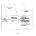
- FIG. 1 is a schematic block diagram of a communications device in accordance with the present invention.
- FIG. 2 is a more detailed schematic block diagram of the communications device of FIG. 1 .
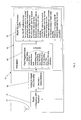
- FIG. 3 is a flowchart illustrating operation of the communications device of FIG. 2 .
- the communications device 10 includes a radio frequency (RF) receiver 12 that is scannable over a plurality of different frequencies.
- the RF receiver 12 is coupled to an analog to digital (AD) converter 14 .
- the AD converter 14 is configured to generate a receive bitstream based upon the RF signal received by the RF receiver.
- a processor 10 is coupled to the AD converter 14 and the RF receiver 12 , and is capable of performing multiple operations in parallel.
- the processor 10 in parallel, calculates a received power level from the receive bitstream, attempts analog video decoding from the receive bitstream, and attempts digital video decoding from the receive bitstream.
- the single AD converter 14 feeds the processor 10 , which then performs the above operations in parallel. This advantageously increases performance over a prior art system that would use three separate AD converters in parallel.
- the processor also scans the RF receiver 12 to a next frequency based upon the received power level, and locks the RF receiver 12 to a current frequency based on the attempted analog and video decoding.
- the communications device 10' includes an RF receiver 12' with a multiband antenna 11' coupled thereto.
- the multiband antenna 11' may be capable of scanning the L (1.7-1.85GHz), S (2.2-2.5GHz), and C (4.4-5.8GHz) bands, although it additionally or alternatively it may be capable of scanning other bands.
- the RF receiver 12' is scannable over a plurality of frequencies and frequency bands, and may process an incoming signal, for example converting it to a baseband signal, as will be appreciated by those of skill in the art.
- a single AD converter 14 ' is coupled to the RF receiver 12 '.
- a processor 16' is coupled to the single AD converter 14 ' and the RF receiver 12 ', and comprises a field programmable gate array (FPGA) 18 ' coupled to a digital signal processor (DSP) 20'.
- the DSP 20' controls which frequency the RF receiver 12 ' scans at. It should be understood, though, that in some embodiments, the processor 12 ' may comprise a single central processing unit, and may not include a FPGA 18 '.
- the FPGA 18' includes at least three parallel logic paths.
- the first logic path includes logic circuitry configured to calculate a received power level of the receive bitstream.
- the second logic path includes logic circuitry configured to attempt analog video decoding of the receive bitstream, and the third logic path includes logic circuitry configured to attempt digital video decoding of the receive bitstream.
- the communications RF receiver 12 ' scans a frequency (Block 32 ).
- the single AD converter 14 ' then generates a receive bitstream based upon the RF signal received by the RF receiver 12 ' (Block 33 ).
- the bitsream is a digital representation of the incoming signal as passed to the single AD converter 14 ' by the RF receiver 12 '.
- the FPGA 18' calculates a received power level from the receive bitstream (Block 35 ), attempts analog video decoding of the receive bitstream (Block 34 ), and attempts digital video decoding of the receive bitstream (Block 36).
- Block 35 a received power level from the receive bitstream
- Block 34 attempts analog video decoding of the receive bitstream
- Block 36 attempts digital video decoding of the receive bitstream
- Calculation of the received power level may include calculating an average power of the receive bitstream, for example, although other calculations may additionally or alternatively be performed.
- the attempted analog video decoding may be a frequency modulated National Television Service Committee (FM NTSC) decoding, for example, although other types of analog video decoding may be used as well.
- the attempted digital video decoding may be a frequency-shift keying (FSK) video decoding, although other types of digital video decoding may of course be used.
- FM NTSC National Television Service Committee
- FSK frequency-shift keying
- each logic path of the FPGA 18' is fed to the DSP 20 '.
- the DSP 20 ' receives the output of each logic path as soon as the receive bitstream propagates therethrough.
- the DSP 20 ' compares the received power level with a threshold to determine whether a RF signal has been detected (Block 37 ). If the received power level is less than the threshold, the DSP 20 ' scans the RF receiver 12 ' to a next frequency (Block 32 ).
- the DSP 20 ' After determining whether a RF signal has been detected, if the DSP 20 ' receives an unsuccessful analog video decoding determination and unsuccessful digital video decoding (Block 38 ) determination from the FPGA 18 ', it scans the RF receiver to a next frequency (Block 32 ) and the process begins anew, repeating until a video signal has been found.
- the process of scanning a given frequency range for video signals is significantly sped up. For example, determining the received power level is very quick. Therefore, before attempted analog or digital decoding can be completed, the calculation of a received power level of a given frequency will be complete. If the received power level is below a threshold, the processor scans the RF receiver to a next frequency, saving time, as continuing the attempted analog and digital detection would be fruitless.
- a video signal may be detected on frequencies up to 2MHz greater than, and up to 2MHz less than, a carrier frequency of the video signal. For this reason, the DSP 20' increments the frequency at which the RF receiver 12 ' scans by 4MHz when the receiver power level is less than the threshold, or when no analog or video signals are detected.
- the DSP 20 If the DSP 20 ' receives a successful analog video decoding of the receive bitstream or a successful digital video decoding of the receive bitstream (Block 37 ), it performs a fine tuning of the current frequency via a frequency offset calculation, such as a DC error calculation (Block 39 ).
- a frequency offset calculation such as a DC error calculation
- the fine tuning may be performed by averaging the derivative of the phase of the signal over time, and the resulting number has a liner relationship with the frequency offset.
- the DSP 20' reads the result and increments the RF receiver 12 ' by .5MHz for every 2,000 units of frequency offset found, if the frequency offset is positive, and by -.5MHz for every 2,000 units of frequency offset found, if the frequency offset is negative.
- the DSP 20 ' then locks the RF receiver 12 ' to the current frequency after fine tuning (Block 40 ), and the process ends (Block 41 ).
- the current frequency may have changed during the fine tuning, based upon the frequency offset calculation.
- a video signal broadcast at a given frequency may be detected on a range of frequencies including the given frequency, although best reception will occur on the given frequency itself. Therefore, the FPGA 18' may detect a video signal on the current frequency, but the current frequency may not provide for the best reception of the video signal.
- the frequency offset calculation may be used to find the frequency for best reception of the video signal, and the current frequency at which the RF receiver 12 ' is scanning may be adjusted accordingly.
- the frequency offset calculation is typically able to pinpoint the frequency for best reception of an analog video signal if it is within a 4MHz window of the current signal, while it is typically able to pinpoint the frequency for best reception of a digital video signal if it is within a 1MHz window of the current signal.
- the DSP 20 ' switches off the unsuccessful logic path in favor of the successful logic path. That is, if the DSP 20 ' receives a successful digital video decoding from the FPGA 18 ', it will switch off the analog video decoding logic path. The decoded digital video may then be stored or displayed by a storage device or display, respectively.
Landscapes
- Engineering & Computer Science (AREA)
- Multimedia (AREA)
- Signal Processing (AREA)
- Circuits Of Receivers In General (AREA)
- Channel Selection Circuits, Automatic Tuning Circuits (AREA)
Abstract
Description
- The present invention relates to the field of wireless video communications, and, more particularly, to a radio frequency (RF) communications device for differentiating RF analog video communications from RF digital video communications and related methods.
- RF transmission of video signals is commonly performed for certain applications. For example, television stations routinely broadcast such video signals on a variety of frequency bands, which may then be received and displayed by television sets. Furthermore, unmanned surveillance aircraft used for crowd observation also broadcast video signals on a variety of frequency bands. Tuning a receiver to a known frequency to receive a video signal transmitted on that frequency is quick and simple. However, when no specific frequency is known, and instead merely a band of frequencies, tuning a receiver to find a video signal being transmitted at a given frequency within the band of frequencies can be time consuming, as each frequency within the band may be checked.
- To add to this difficulty of finding a given frequency on which the video signal is being transmitted, the video signal may be an analog or a digital video signal. Therefore, when both the form (analog or digital) of the video signal and the given frequency on which it is being transmitted are unknown, a separate analog and a separate digital receiver are typically used to find the video signal. Each receiver is made to scan each frequency of the band. As such, detection of a video signal with an unknown form and being transmitted on an unknown frequency can be time consuming for even advanced hardware.
- Attempts at making receivers to speed up this process have been made. For example,
U.S. Pat. Pub. 2009/0122205 to Xing et al. discloses a television receiver including separate analog and digital video tuners. Each tuner is configured to separately scan a plurality of channels for a video signal. An analog decoder determines whether the analog video tuner has found a video signal on a given channel, while a digital decoder determines whether the digital video tuner has found a video signal on the given channel. The television receiver of Xing et al., however, suffers from some drawbacks. For example, both the analog and the digital tuner check each channel for the presence of a video signal, even though one of the tuners may have determined that there is no signal on a given channel. -
U.S. Pat. No. 7,322,039 to Tsubouchi et al. discloses a broadcasting receiver for receiving analog and digital video signals. The broadcasting receiver includes an analog tuner and a digital tuner. The analog tuner and the digital tuner are configured to concurrently scan a plurality of channels for video signals. A main CPU determines whether the digital tuner has found a digital video signal, while a sub-CPU determines whether the analog tuner has found an analog video signal. Tsubouchi et al. suffers from similar drawbacks to Xing et al., however. Both the analog and the digital tuner check each channel for the presence of a video signal, even though one of the tuners may have determined that there is no signal on a given channel. - Given the drawbacks of the prior art, further advances in communications devices able to scan a range of frequencies for analog and digital video signals may be desirable.
- In view of the foregoing background, it is therefore an object of the present invention to provide a communications device able to quickly scan a range of frequencies for a video signal and determine if the video signal is an analog video signal or a digital video signal.
- This and other objects, features, and advantages in accordance with the present invention are provided by a communications device comprising a radio frequency (RF) receiver being scannable over a plurality of different frequencies. An analog to digital (AD) converter is coupled to the RF receiver and is configured to generate a receive bitstream. A processor is coupled to the RF receiver and the AD converter. The processor is configured to perform in parallel calculating a received power level from the receive bitstream, attempting analog video decoding from the receive bitstream, and attempting digital video decoding from the receive bitstream. The processor is also configured to lock the RF receiver to a current frequency or scan the RF receiver to a next frequency based upon the received power level, and the attempted analog and video decoding. The processor may scan the RF receiver to a next frequency based upon the received power level being below a threshold.
- By calculating the received power level, attempting analog decoding, and attempting digital decoding in parallel, the process of scanning a given frequency range for video signals is significantly sped up. For example, determining the received power level is very quick. Therefore, before attempted analog or digital decoding can be completed, the calculation of a received power level of a given frequency will be complete. If the received power level is below a threshold, the processor scans the RF receiver to a next frequency, saving time, as continuing the attempted analog and digital detection would be fruitless.
- In addition, the processor may also scan the RF receiver to a next frequency based upon the received power level being above a threshold, and based upon a failure of attempted analog and video decoding. Furthermore, the processor may lock the RF receiver to a current frequency based upon the received power level being above a threshold, and based upon a success of one of attempted analog and digital video decoding.
- The processor may also be configured to perform a frequency offset calculation (e.g. a DC offset calculation) and to perform a fine tuning of the RF receiver based upon the frequency offset calculation. This fine tuning allows the processor to quickly scan the RF receiver to the proper frequency on which to receive the video signal, saving time over conventional communications devices which would scan all frequencies within a frequency band to find the proper frequency.
- In some applications, the processor may comprise a field programmable gate array (FPGA) and a digital signal processor (DSP) coupled thereto. The FPGA may be configured to perform, in parallel, the calculation of the received power level, the attempted analog video decoding, and the attempted digital video decoding. The DSP may be configured to lock the RF receiver to the current frequency or scan the RF receiver to the next frequency.
- The analog video decoding may comprise a frequency modulated National Television System Committee (FM NTSC) decoding. In addition, the digital video decoding may comprise a frequency-shift keying (FSK) video decoding. A multiband antenna may be coupled to the RF receiver.
- A method aspect is directed to a method of operating a communications device. The method may include generating a receive bitstream using an analog to digital (AD) converter coupled to a radio frequency (RF) receiver. The method may also include performing in parallel, using a processor coupled to the AD converter and the RF receiver, a calculation of a received power level from the receive bitstream, an attempted analog video decoding of the receive bitstream, and an attempted digital video decoding of the receive bitstream. In addition, the method may include locking the RF receiver to a current frequency or scanning the RF receiver to a next frequency based upon the received power level, and the attempted analog and video decoding, using the processor.
-
FIG. 1 is a schematic block diagram of a communications device in accordance with the present invention. -
FIG. 2 is a more detailed schematic block diagram of the communications device ofFIG. 1 . -
FIG. 3 is a flowchart illustrating operation of the communications device ofFIG. 2 . - The present invention will now be described more fully hereinafter with reference to the accompanying drawings, in which preferred embodiments of the invention are shown. This invention may, however, be embodied in many different forms and should not be construed as limited to the embodiments set forth herein. Rather, these embodiments are provided so that this disclosure will be thorough and complete, and will fully convey the scope of the invention to those skilled in the art. Like numbers refer to like elements throughout, and prime notation is used to indicate similar elements in alternative embodiments.
- Referring initially to
FIG. 1 , acommunications device 10 is now generally described. More specific details will be given below. Thecommunications device 10 includes a radio frequency (RF)receiver 12 that is scannable over a plurality of different frequencies. TheRF receiver 12 is coupled to an analog to digital (AD)converter 14. TheAD converter 14 is configured to generate a receive bitstream based upon the RF signal received by the RF receiver. Aprocessor 10 is coupled to theAD converter 14 and theRF receiver 12, and is capable of performing multiple operations in parallel. Theprocessor 10, in parallel, calculates a received power level from the receive bitstream, attempts analog video decoding from the receive bitstream, and attempts digital video decoding from the receive bitstream. It should be noted that thesingle AD converter 14 feeds theprocessor 10, which then performs the above operations in parallel. This advantageously increases performance over a prior art system that would use three separate AD converters in parallel. - The processor also scans the
RF receiver 12 to a next frequency based upon the received power level, and locks theRF receiver 12 to a current frequency based on the attempted analog and video decoding. - Referring now to the communications device 10' of
FIG. 2 a more detailed description of the communications device is now given. The communications device 10' includes an RF receiver 12' with a multiband antenna 11' coupled thereto. The multiband antenna 11' may be capable of scanning the L (1.7-1.85GHz), S (2.2-2.5GHz), and C (4.4-5.8GHz) bands, although it additionally or alternatively it may be capable of scanning other bands. The RF receiver 12' is scannable over a plurality of frequencies and frequency bands, and may process an incoming signal, for example converting it to a baseband signal, as will be appreciated by those of skill in the art. A single AD converter 14' is coupled to the RF receiver 12'. A processor 16' is coupled to the single AD converter 14' and the RF receiver 12', and comprises a field programmable gate array (FPGA) 18' coupled to a digital signal processor (DSP) 20'. The DSP 20' controls which frequency the RF receiver 12' scans at. It should be understood, though, that in some embodiments, the processor 12' may comprise a single central processing unit, and may not include a FPGA 18'. - The FPGA 18' includes at least three parallel logic paths. The first logic path includes logic circuitry configured to calculate a received power level of the receive bitstream. The second logic path includes logic circuitry configured to attempt analog video decoding of the receive bitstream, and the third logic path includes logic circuitry configured to attempt digital video decoding of the receive bitstream.
- Referring additionally to the
flowchart 30 ofFIG. 3 , operation of the communications device 10' is now described. After the start (Block 31), the communications RF receiver 12' scans a frequency (Block 32). The single AD converter 14' then generates a receive bitstream based upon the RF signal received by the RF receiver 12' (Block 33). The bitsream is a digital representation of the incoming signal as passed to the single AD converter 14' by the RF receiver 12'. Once again, it should be noted that a single AD converter 14' passes a signal along to the FPGA 18', and not multiple AD converters working on parallel. - Next, the FPGA 18', in parallel, calculates a received power level from the receive bitstream (Block 35), attempts analog video decoding of the receive bitstream (Block 34), and attempts digital video decoding of the receive bitstream (Block 36). By "in parallel," it should be understood that the FPGA 18' performs these functions simultaneously, via separate logic paths.
- Calculation of the received power level may include calculating an average power of the receive bitstream, for example, although other calculations may additionally or alternatively be performed. The attempted analog video decoding may be a frequency modulated National Television Service Committee (FM NTSC) decoding, for example, although other types of analog video decoding may be used as well. The attempted digital video decoding may be a frequency-shift keying (FSK) video decoding, although other types of digital video decoding may of course be used.
- The output of each logic path of the FPGA 18' is fed to the DSP 20'. As such, the DSP 20' receives the output of each logic path as soon as the receive bitstream propagates therethrough. The DSP 20' compares the received power level with a threshold to determine whether a RF signal has been detected (Block 37). If the received power level is less than the threshold, the DSP 20' scans the RF receiver 12' to a next frequency (Block 32). After determining whether a RF signal has been detected, if the DSP 20' receives an unsuccessful analog video decoding determination and unsuccessful digital video decoding (Block 38) determination from the FPGA 18', it scans the RF receiver to a next frequency (Block 32) and the process begins anew, repeating until a video signal has been found.
- By calculating the received power level, attempting analog decoding, and attempting digital decoding in parallel, the process of scanning a given frequency range for video signals is significantly sped up. For example, determining the received power level is very quick. Therefore, before attempted analog or digital decoding can be completed, the calculation of a received power level of a given frequency will be complete. If the received power level is below a threshold, the processor scans the RF receiver to a next frequency, saving time, as continuing the attempted analog and digital detection would be fruitless.
- In general, a video signal may be detected on frequencies up to 2MHz greater than, and up to 2MHz less than, a carrier frequency of the video signal. For this reason, the DSP 20' increments the frequency at which the RF receiver 12' scans by 4MHz when the receiver power level is less than the threshold, or when no analog or video signals are detected.
- If the DSP 20' receives a successful analog video decoding of the receive bitstream or a successful digital video decoding of the receive bitstream (Block 37), it performs a fine tuning of the current frequency via a frequency offset calculation, such as a DC error calculation (Block 39).
- The fine tuning may be performed by averaging the derivative of the phase of the signal over time, and the resulting number has a liner relationship with the frequency offset. The DSP 20' reads the result and increments the RF receiver 12' by .5MHz for every 2,000 units of frequency offset found, if the frequency offset is positive, and by -.5MHz for every 2,000 units of frequency offset found, if the frequency offset is negative. The DSP 20' then locks the RF receiver 12' to the current frequency after fine tuning (Block 40), and the process ends (Block 41).
- It should be noted that the current frequency may have changed during the fine tuning, based upon the frequency offset calculation. As will be appreciated by those of skill in the art, a video signal broadcast at a given frequency may be detected on a range of frequencies including the given frequency, although best reception will occur on the given frequency itself. Therefore, the FPGA 18' may detect a video signal on the current frequency, but the current frequency may not provide for the best reception of the video signal. The frequency offset calculation may be used to find the frequency for best reception of the video signal, and the current frequency at which the RF receiver 12' is scanning may be adjusted accordingly. The frequency offset calculation is typically able to pinpoint the frequency for best reception of an analog video signal if it is within a 4MHz window of the current signal, while it is typically able to pinpoint the frequency for best reception of a digital video signal if it is within a 1MHz window of the current signal.
- Furthermore, the DSP 20' switches off the unsuccessful logic path in favor of the successful logic path. That is, if the DSP 20' receives a successful digital video decoding from the FPGA 18', it will switch off the analog video decoding logic path. The decoded digital video may then be stored or displayed by a storage device or display, respectively.
Claims (10)
- A communications device comprising:a radio frequency (RF) receiver being scannable over a plurality of different frequencies;an analog to digital (AD) converter coupled to said RF receiver and configured to generate a receive bitstream; anda processor coupled to said RF receiver and said AD converter and configured to perform in parallel
calculating a received power level from the receive bitstream,
attempting analog video decoding from the receive bitstream, and
attempting digital video decoding from the receive bitstream;said processor also configured to lock said RF receiver to a current frequency or scan said RF receiver to a next frequency based upon the received power level, and the attempted analog and video decoding. - The communications device of Claim 1 wherein said processor scans said RF receiver to the next frequency based upon the received power level being below a threshold.
- The communications device of Claim 1 wherein said processor scans said RF receiver to the next frequency based upon the received power level being above a threshold, and based upon a failure of attempted analog and digital video decoding.
- The communications device of Claim 1 wherein said processor locks said RF receiver to a current frequency based upon the received power level being above a threshold, and based upon a success of one of attempted analog and digital video decoding.
- The communications device of Claim 1 wherein said processor is also configured to perform a Frequency offset calculation, and perform a fine tuning of said RF receiver based upon the Frequency offset calculation.
- The communications device of Claim 1 wherein said processor comprises a field programmable gate array (FPGA) and a digital signal processor (DSP) coupled thereto.
- The communications device of Claim 6 wherein said FPGA is configured to perform, in parallel, the calculation of the received power level, the attempted analog video decoding, and the attempted digital video decoding; and wherein said DSP is configured to lock said RF receiver to the current frequency or scan said RF receiver to the next frequency.
- A method of operating a communications device comprising:generating a receive bitstream using an analog to digital (AD) converter coupled to a radio frequency (RF) receiver;performing in parallel, using a processor coupled to the AD converter and the RF receiver,
a calculation of a received power level from the receive bitstream,
an attempted analog video decoding of the receive bitstream, and
an attempted digital video decoding of the receive bitstream; andlocking the RF receiver to a current frequency or scanning the RF receiver to a next frequency based upon the received power level, and the attempted analog and video decoding, using the processor. - The method of Claim 8 wherein the RF receiver is scanned to a next frequency based upon the received power level being below a threshold.
- The method of Claim 8 wherein the RF receiver is scanned to a next frequency based upon the received power level being above a threshold, and based upon a failure of attempted analog and digital video decoding.
Applications Claiming Priority (1)
| Application Number | Priority Date | Filing Date | Title |
|---|---|---|---|
| US12/779,505 US8379732B2 (en) | 2010-05-13 | 2010-05-13 | Communications device for scanning multiple frequencies and for detecting analog and digital video signals and associated methods |
Publications (3)
| Publication Number | Publication Date |
|---|---|
| EP2387234A1 true EP2387234A1 (en) | 2011-11-16 |
| EP2387234A8 EP2387234A8 (en) | 2011-12-21 |
| EP2387234B1 EP2387234B1 (en) | 2014-07-09 |
Family
ID=44262641
Family Applications (1)
| Application Number | Title | Priority Date | Filing Date |
|---|---|---|---|
| EP11003927.8A Active EP2387234B1 (en) | 2010-05-13 | 2011-05-12 | Communications device for scanning multiple frequencies and for detecting analog and digital video signals and associated methods |
Country Status (3)
| Country | Link |
|---|---|
| US (1) | US8379732B2 (en) |
| EP (1) | EP2387234B1 (en) |
| IL (1) | IL212295A (en) |
Families Citing this family (2)
| Publication number | Priority date | Publication date | Assignee | Title |
|---|---|---|---|---|
| US9374063B1 (en) * | 2015-02-05 | 2016-06-21 | University Of Macau | Gain-boosted N-path bandpass filter |
| EP4311113B1 (en) | 2022-07-21 | 2026-04-08 | Rohde & Schwarz GmbH & Co. KG | Radio frequency receiver and operation method thereof |
Citations (5)
| Publication number | Priority date | Publication date | Assignee | Title |
|---|---|---|---|---|
| US20020097344A1 (en) * | 2001-01-22 | 2002-07-25 | Toru Shibusawa | Digital broadcasting receiver and channel information registration processing method in digital broadcasting receiver |
| US20040036811A1 (en) * | 2002-08-22 | 2004-02-26 | Yasuyuki Ikeguchi | Broadcasting receiver and channel searching method in broadcasting receiver |
| US7322039B2 (en) | 2000-12-01 | 2008-01-22 | Sanyo Electric Co., Ltd. | Digital and analog broadcasting receiver |
| WO2009018766A1 (en) * | 2007-08-08 | 2009-02-12 | Mediatek Inc. | Apparatuses and methods for scanning digital and analog television channels |
| US20090122205A1 (en) | 2005-11-29 | 2009-05-14 | Joseph J. Laks Thomson Licensing Llc | Method and Apparatus for Performing a Channel Search |
Family Cites Families (6)
| Publication number | Priority date | Publication date | Assignee | Title |
|---|---|---|---|---|
| JP3589178B2 (en) * | 2000-11-29 | 2004-11-17 | 船井電機株式会社 | Digital / analog television signal receiver |
| JP3888167B2 (en) * | 2002-01-18 | 2007-02-28 | 船井電機株式会社 | Digital / analog broadcast receiver with high-speed scanning function for broadcast channels |
| US7265793B2 (en) * | 2004-02-17 | 2007-09-04 | Broadcom Corporation | Method and system for detecting digital QAM, VSB and analog TV signals |
| US7707611B2 (en) * | 2006-07-24 | 2010-04-27 | Newport Media, Inc. | Receiver with a visual program guide for mobile television applications and method for creation |
| US7957296B2 (en) * | 2007-01-02 | 2011-06-07 | Intel Corporation | Apparatus for and method of detecting loss of signal in a radio frequency cable |
| US20080304596A1 (en) * | 2007-06-11 | 2008-12-11 | Loke Tan | Method and System for Receiving Audio, Video and Data Services with ATSC Enabled Television Sets |
-
2010
- 2010-05-13 US US12/779,505 patent/US8379732B2/en active Active
-
2011
- 2011-04-13 IL IL212295A patent/IL212295A/en active IP Right Grant
- 2011-05-12 EP EP11003927.8A patent/EP2387234B1/en active Active
Patent Citations (5)
| Publication number | Priority date | Publication date | Assignee | Title |
|---|---|---|---|---|
| US7322039B2 (en) | 2000-12-01 | 2008-01-22 | Sanyo Electric Co., Ltd. | Digital and analog broadcasting receiver |
| US20020097344A1 (en) * | 2001-01-22 | 2002-07-25 | Toru Shibusawa | Digital broadcasting receiver and channel information registration processing method in digital broadcasting receiver |
| US20040036811A1 (en) * | 2002-08-22 | 2004-02-26 | Yasuyuki Ikeguchi | Broadcasting receiver and channel searching method in broadcasting receiver |
| US20090122205A1 (en) | 2005-11-29 | 2009-05-14 | Joseph J. Laks Thomson Licensing Llc | Method and Apparatus for Performing a Channel Search |
| WO2009018766A1 (en) * | 2007-08-08 | 2009-02-12 | Mediatek Inc. | Apparatuses and methods for scanning digital and analog television channels |
Also Published As
| Publication number | Publication date |
|---|---|
| US20110280313A1 (en) | 2011-11-17 |
| EP2387234A8 (en) | 2011-12-21 |
| EP2387234B1 (en) | 2014-07-09 |
| US8379732B2 (en) | 2013-02-19 |
| IL212295A0 (en) | 2011-06-30 |
| IL212295A (en) | 2015-04-30 |
Similar Documents
| Publication | Publication Date | Title |
|---|---|---|
| JP3920575B2 (en) | Channel information registration processing method in digital broadcast receiver | |
| US9184776B2 (en) | Signal tuning with variable intermediate frequency for image rejection and methods | |
| US8320821B2 (en) | Receiving apparatus | |
| EP2387234B1 (en) | Communications device for scanning multiple frequencies and for detecting analog and digital video signals and associated methods | |
| KR101092698B1 (en) | Digital multimedia broadcasting system and method thereof for reducing scan time | |
| US6437837B1 (en) | Digital broadcast signal processing apparatus and method in which channel interference by analog broadcast is prevented | |
| KR19980079568A (en) | Digital television receiver detects entity interference by using video signal from auxiliary analog television receiver | |
| US8036324B2 (en) | Digital broadcasting receiving apparatus | |
| US9531414B2 (en) | Management process of a radio service following in a receptor and corresponding receptor | |
| EP1406402A2 (en) | Improved digital broadcast receiver | |
| JP6522979B2 (en) | TV receiver | |
| RU2562423C2 (en) | Method and system for receiving signals from radio station | |
| US8441580B2 (en) | Method and system for scanning a frequency channel in digital television | |
| US10122482B1 (en) | Radio receiver system | |
| JP3798604B2 (en) | Broadcast system discrimination device and broadcast system discrimination method | |
| JPH10190505A (en) | Satellite broadcast receiver | |
| KR100413410B1 (en) | Automatic setting of local oscillation frequency of low noise block of satellite broadcasting receiver | |
| JP3959761B2 (en) | Satellite broadcasting receiver | |
| EP1631079A1 (en) | A mobile television receiver and method for automatically identifying the transmission standard of broadcast television signals | |
| KR101525052B1 (en) | Apparatus and method for improving frequency search speed in OFDM system | |
| KR101148360B1 (en) | Channel search method of RF signal processing circuit | |
| JP2005303587A (en) | Receiver | |
| JP4179040B2 (en) | Receiving device and booster device | |
| JP5669570B2 (en) | Broadcast receiver | |
| KR20090115458A (en) | Image Channel Removal Device and Method |
Legal Events
| Date | Code | Title | Description |
|---|---|---|---|
| 17P | Request for examination filed |
Effective date: 20110512 |
|
| AK | Designated contracting states |
Kind code of ref document: A1 Designated state(s): AL AT BE BG CH CY CZ DE DK EE ES FI FR GB GR HR HU IE IS IT LI LT LU LV MC MK MT NL NO PL PT RO RS SE SI SK SM TR |
|
| AX | Request for extension of the european patent |
Extension state: BA ME |
|
| PUAI | Public reference made under article 153(3) epc to a published international application that has entered the european phase |
Free format text: ORIGINAL CODE: 0009012 |
|
| RAP1 | Party data changed (applicant data changed or rights of an application transferred) |
Owner name: HARRIS CORPORATION |
|
| RAP1 | Party data changed (applicant data changed or rights of an application transferred) |
Owner name: HARRIS CORPORATION |
|
| GRAP | Despatch of communication of intention to grant a patent |
Free format text: ORIGINAL CODE: EPIDOSNIGR1 |
|
| INTG | Intention to grant announced |
Effective date: 20131213 |
|
| GRAS | Grant fee paid |
Free format text: ORIGINAL CODE: EPIDOSNIGR3 |
|
| GRAP | Despatch of communication of intention to grant a patent |
Free format text: ORIGINAL CODE: EPIDOSNIGR1 |
|
| INTG | Intention to grant announced |
Effective date: 20140429 |
|
| GRAA | (expected) grant |
Free format text: ORIGINAL CODE: 0009210 |
|
| AK | Designated contracting states |
Kind code of ref document: B1 Designated state(s): AL AT BE BG CH CY CZ DE DK EE ES FI FR GB GR HR HU IE IS IT LI LT LU LV MC MK MT NL NO PL PT RO RS SE SI SK SM TR |
|
| REG | Reference to a national code |
Ref country code: GB Ref legal event code: FG4D |
|
| REG | Reference to a national code |
Ref country code: CH Ref legal event code: EP Ref country code: AT Ref legal event code: REF Ref document number: 676919 Country of ref document: AT Kind code of ref document: T Effective date: 20140715 |
|
| REG | Reference to a national code |
Ref country code: IE Ref legal event code: FG4D |
|
| REG | Reference to a national code |
Ref country code: DE Ref legal event code: R096 Ref document number: 602011008209 Country of ref document: DE Effective date: 20140821 |
|
| REG | Reference to a national code |
Ref country code: AT Ref legal event code: MK05 Ref document number: 676919 Country of ref document: AT Kind code of ref document: T Effective date: 20140709 |
|
| REG | Reference to a national code |
Ref country code: NL Ref legal event code: VDEP Effective date: 20140709 |
|
| REG | Reference to a national code |
Ref country code: LT Ref legal event code: MG4D |
|
| PG25 | Lapsed in a contracting state [announced via postgrant information from national office to epo] |
Ref country code: LT Free format text: LAPSE BECAUSE OF FAILURE TO SUBMIT A TRANSLATION OF THE DESCRIPTION OR TO PAY THE FEE WITHIN THE PRESCRIBED TIME-LIMIT Effective date: 20140709 Ref country code: FI Free format text: LAPSE BECAUSE OF FAILURE TO SUBMIT A TRANSLATION OF THE DESCRIPTION OR TO PAY THE FEE WITHIN THE PRESCRIBED TIME-LIMIT Effective date: 20140709 Ref country code: SE Free format text: LAPSE BECAUSE OF FAILURE TO SUBMIT A TRANSLATION OF THE DESCRIPTION OR TO PAY THE FEE WITHIN THE PRESCRIBED TIME-LIMIT Effective date: 20140709 Ref country code: PT Free format text: LAPSE BECAUSE OF FAILURE TO SUBMIT A TRANSLATION OF THE DESCRIPTION OR TO PAY THE FEE WITHIN THE PRESCRIBED TIME-LIMIT Effective date: 20141110 Ref country code: GR Free format text: LAPSE BECAUSE OF FAILURE TO SUBMIT A TRANSLATION OF THE DESCRIPTION OR TO PAY THE FEE WITHIN THE PRESCRIBED TIME-LIMIT Effective date: 20141010 Ref country code: NO Free format text: LAPSE BECAUSE OF FAILURE TO SUBMIT A TRANSLATION OF THE DESCRIPTION OR TO PAY THE FEE WITHIN THE PRESCRIBED TIME-LIMIT Effective date: 20141009 Ref country code: ES Free format text: LAPSE BECAUSE OF FAILURE TO SUBMIT A TRANSLATION OF THE DESCRIPTION OR TO PAY THE FEE WITHIN THE PRESCRIBED TIME-LIMIT Effective date: 20140709 Ref country code: BG Free format text: LAPSE BECAUSE OF FAILURE TO SUBMIT A TRANSLATION OF THE DESCRIPTION OR TO PAY THE FEE WITHIN THE PRESCRIBED TIME-LIMIT Effective date: 20141009 |
|
| PG25 | Lapsed in a contracting state [announced via postgrant information from national office to epo] |
Ref country code: LV Free format text: LAPSE BECAUSE OF FAILURE TO SUBMIT A TRANSLATION OF THE DESCRIPTION OR TO PAY THE FEE WITHIN THE PRESCRIBED TIME-LIMIT Effective date: 20140709 Ref country code: AT Free format text: LAPSE BECAUSE OF FAILURE TO SUBMIT A TRANSLATION OF THE DESCRIPTION OR TO PAY THE FEE WITHIN THE PRESCRIBED TIME-LIMIT Effective date: 20140709 Ref country code: RS Free format text: LAPSE BECAUSE OF FAILURE TO SUBMIT A TRANSLATION OF THE DESCRIPTION OR TO PAY THE FEE WITHIN THE PRESCRIBED TIME-LIMIT Effective date: 20140709 Ref country code: HR Free format text: LAPSE BECAUSE OF FAILURE TO SUBMIT A TRANSLATION OF THE DESCRIPTION OR TO PAY THE FEE WITHIN THE PRESCRIBED TIME-LIMIT Effective date: 20140709 Ref country code: IS Free format text: LAPSE BECAUSE OF FAILURE TO SUBMIT A TRANSLATION OF THE DESCRIPTION OR TO PAY THE FEE WITHIN THE PRESCRIBED TIME-LIMIT Effective date: 20141109 Ref country code: NL Free format text: LAPSE BECAUSE OF FAILURE TO SUBMIT A TRANSLATION OF THE DESCRIPTION OR TO PAY THE FEE WITHIN THE PRESCRIBED TIME-LIMIT Effective date: 20140709 Ref country code: CY Free format text: LAPSE BECAUSE OF FAILURE TO SUBMIT A TRANSLATION OF THE DESCRIPTION OR TO PAY THE FEE WITHIN THE PRESCRIBED TIME-LIMIT Effective date: 20140709 Ref country code: PL Free format text: LAPSE BECAUSE OF FAILURE TO SUBMIT A TRANSLATION OF THE DESCRIPTION OR TO PAY THE FEE WITHIN THE PRESCRIBED TIME-LIMIT Effective date: 20140709 |
|
| REG | Reference to a national code |
Ref country code: DE Ref legal event code: R097 Ref document number: 602011008209 Country of ref document: DE |
|
| PG25 | Lapsed in a contracting state [announced via postgrant information from national office to epo] |
Ref country code: CZ Free format text: LAPSE BECAUSE OF FAILURE TO SUBMIT A TRANSLATION OF THE DESCRIPTION OR TO PAY THE FEE WITHIN THE PRESCRIBED TIME-LIMIT Effective date: 20140709 Ref country code: SK Free format text: LAPSE BECAUSE OF FAILURE TO SUBMIT A TRANSLATION OF THE DESCRIPTION OR TO PAY THE FEE WITHIN THE PRESCRIBED TIME-LIMIT Effective date: 20140709 Ref country code: DK Free format text: LAPSE BECAUSE OF FAILURE TO SUBMIT A TRANSLATION OF THE DESCRIPTION OR TO PAY THE FEE WITHIN THE PRESCRIBED TIME-LIMIT Effective date: 20140709 Ref country code: EE Free format text: LAPSE BECAUSE OF FAILURE TO SUBMIT A TRANSLATION OF THE DESCRIPTION OR TO PAY THE FEE WITHIN THE PRESCRIBED TIME-LIMIT Effective date: 20140709 Ref country code: RO Free format text: LAPSE BECAUSE OF FAILURE TO SUBMIT A TRANSLATION OF THE DESCRIPTION OR TO PAY THE FEE WITHIN THE PRESCRIBED TIME-LIMIT Effective date: 20140709 |
|
| PLBE | No opposition filed within time limit |
Free format text: ORIGINAL CODE: 0009261 |
|
| STAA | Information on the status of an ep patent application or granted ep patent |
Free format text: STATUS: NO OPPOSITION FILED WITHIN TIME LIMIT |
|
| 26N | No opposition filed |
Effective date: 20150410 |
|
| PG25 | Lapsed in a contracting state [announced via postgrant information from national office to epo] |
Ref country code: SI Free format text: LAPSE BECAUSE OF FAILURE TO SUBMIT A TRANSLATION OF THE DESCRIPTION OR TO PAY THE FEE WITHIN THE PRESCRIBED TIME-LIMIT Effective date: 20140709 |
|
| REG | Reference to a national code |
Ref country code: CH Ref legal event code: PL |
|
| PG25 | Lapsed in a contracting state [announced via postgrant information from national office to epo] |
Ref country code: LI Free format text: LAPSE BECAUSE OF NON-PAYMENT OF DUE FEES Effective date: 20150531 Ref country code: CH Free format text: LAPSE BECAUSE OF NON-PAYMENT OF DUE FEES Effective date: 20150531 Ref country code: LU Free format text: LAPSE BECAUSE OF FAILURE TO SUBMIT A TRANSLATION OF THE DESCRIPTION OR TO PAY THE FEE WITHIN THE PRESCRIBED TIME-LIMIT Effective date: 20150512 Ref country code: MC Free format text: LAPSE BECAUSE OF FAILURE TO SUBMIT A TRANSLATION OF THE DESCRIPTION OR TO PAY THE FEE WITHIN THE PRESCRIBED TIME-LIMIT Effective date: 20140709 |
|
| REG | Reference to a national code |
Ref country code: IE Ref legal event code: MM4A |
|
| PG25 | Lapsed in a contracting state [announced via postgrant information from national office to epo] |
Ref country code: IE Free format text: LAPSE BECAUSE OF NON-PAYMENT OF DUE FEES Effective date: 20150512 |
|
| REG | Reference to a national code |
Ref country code: FR Ref legal event code: PLFP Year of fee payment: 6 |
|
| PG25 | Lapsed in a contracting state [announced via postgrant information from national office to epo] |
Ref country code: BE Free format text: LAPSE BECAUSE OF FAILURE TO SUBMIT A TRANSLATION OF THE DESCRIPTION OR TO PAY THE FEE WITHIN THE PRESCRIBED TIME-LIMIT Effective date: 20140709 |
|
| PG25 | Lapsed in a contracting state [announced via postgrant information from national office to epo] |
Ref country code: MT Free format text: LAPSE BECAUSE OF FAILURE TO SUBMIT A TRANSLATION OF THE DESCRIPTION OR TO PAY THE FEE WITHIN THE PRESCRIBED TIME-LIMIT Effective date: 20140709 |
|
| REG | Reference to a national code |
Ref country code: FR Ref legal event code: PLFP Year of fee payment: 7 |
|
| PG25 | Lapsed in a contracting state [announced via postgrant information from national office to epo] |
Ref country code: HU Free format text: LAPSE BECAUSE OF FAILURE TO SUBMIT A TRANSLATION OF THE DESCRIPTION OR TO PAY THE FEE WITHIN THE PRESCRIBED TIME-LIMIT; INVALID AB INITIO Effective date: 20110512 Ref country code: SM Free format text: LAPSE BECAUSE OF FAILURE TO SUBMIT A TRANSLATION OF THE DESCRIPTION OR TO PAY THE FEE WITHIN THE PRESCRIBED TIME-LIMIT Effective date: 20140709 |
|
| PG25 | Lapsed in a contracting state [announced via postgrant information from national office to epo] |
Ref country code: TR Free format text: LAPSE BECAUSE OF FAILURE TO SUBMIT A TRANSLATION OF THE DESCRIPTION OR TO PAY THE FEE WITHIN THE PRESCRIBED TIME-LIMIT Effective date: 20140709 |
|
| REG | Reference to a national code |
Ref country code: FR Ref legal event code: PLFP Year of fee payment: 8 |
|
| PG25 | Lapsed in a contracting state [announced via postgrant information from national office to epo] |
Ref country code: MK Free format text: LAPSE BECAUSE OF FAILURE TO SUBMIT A TRANSLATION OF THE DESCRIPTION OR TO PAY THE FEE WITHIN THE PRESCRIBED TIME-LIMIT Effective date: 20140709 |
|
| PG25 | Lapsed in a contracting state [announced via postgrant information from national office to epo] |
Ref country code: AL Free format text: LAPSE BECAUSE OF FAILURE TO SUBMIT A TRANSLATION OF THE DESCRIPTION OR TO PAY THE FEE WITHIN THE PRESCRIBED TIME-LIMIT Effective date: 20140709 |
|
| REG | Reference to a national code |
Ref country code: DE Ref legal event code: R082 Ref document number: 602011008209 Country of ref document: DE Representative=s name: WUESTHOFF & WUESTHOFF, PATENTANWAELTE PARTG MB, DE Ref country code: DE Ref legal event code: R081 Ref document number: 602011008209 Country of ref document: DE Owner name: HARRIS GLOBAL COMMUNICATIONS, INC., ALBANY, US Free format text: FORMER OWNER: HARRIS CORP., MELBOURNE, FLA., US |
|
| REG | Reference to a national code |
Ref country code: GB Ref legal event code: 732E Free format text: REGISTERED BETWEEN 20190207 AND 20190213 |
|
| P01 | Opt-out of the competence of the unified patent court (upc) registered |
Effective date: 20230530 |
|
| PGFP | Annual fee paid to national office [announced via postgrant information from national office to epo] |
Ref country code: DE Payment date: 20250529 Year of fee payment: 15 |
|
| PGFP | Annual fee paid to national office [announced via postgrant information from national office to epo] |
Ref country code: GB Payment date: 20250527 Year of fee payment: 15 |
|
| PGFP | Annual fee paid to national office [announced via postgrant information from national office to epo] |
Ref country code: IT Payment date: 20250521 Year of fee payment: 15 |
|
| PGFP | Annual fee paid to national office [announced via postgrant information from national office to epo] |
Ref country code: FR Payment date: 20250526 Year of fee payment: 15 |