EP2387110A1 - Antenna device - Google Patents
Antenna device Download PDFInfo
- Publication number
- EP2387110A1 EP2387110A1 EP11162590A EP11162590A EP2387110A1 EP 2387110 A1 EP2387110 A1 EP 2387110A1 EP 11162590 A EP11162590 A EP 11162590A EP 11162590 A EP11162590 A EP 11162590A EP 2387110 A1 EP2387110 A1 EP 2387110A1
- Authority
- EP
- European Patent Office
- Prior art keywords
- antenna element
- antenna
- antenna device
- switches
- printed board
- Prior art date
- Legal status (The legal status is an assumption and is not a legal conclusion. Google has not performed a legal analysis and makes no representation as to the accuracy of the status listed.)
- Withdrawn
Links
Images



Classifications
-
- H—ELECTRICITY
- H01—ELECTRIC ELEMENTS
- H01Q—ANTENNAS, i.e. RADIO AERIALS
- H01Q9/00—Electrically-short antennas having dimensions not more than twice the operating wavelength and consisting of conductive active radiating elements
- H01Q9/04—Resonant antennas
- H01Q9/16—Resonant antennas with feed intermediate between the extremities of the antenna, e.g. centre-fed dipole
- H01Q9/26—Resonant antennas with feed intermediate between the extremities of the antenna, e.g. centre-fed dipole with folded element or elements, the folded parts being spaced apart a small fraction of operating wavelength
- H01Q9/27—Spiral antennas
-
- H—ELECTRICITY
- H01—ELECTRIC ELEMENTS
- H01Q—ANTENNAS, i.e. RADIO AERIALS
- H01Q9/00—Electrically-short antennas having dimensions not more than twice the operating wavelength and consisting of conductive active radiating elements
- H01Q9/04—Resonant antennas
- H01Q9/30—Resonant antennas with feed to end of elongated active element, e.g. unipole
- H01Q9/42—Resonant antennas with feed to end of elongated active element, e.g. unipole with folded element, the folded parts being spaced apart a small fraction of the operating wavelength
Definitions
- the present invention relates to an antenna device.
- a device for wireless communication is, for example, an electronic apparatus having a wireless communication function.
- the electronic apparatus may specifically include a wireless terminal such as a mobile phone, a smart phone, a PDA (Personal digital Assistant), a PC (Personal Computer) or a GPS (Global Positioning System) terminal, or a wireless communication application apparatus such as a card for wireless communication (e.g., a PCMCIA card).
- a wireless terminal such as a mobile phone, a smart phone, a PDA (Personal digital Assistant), a PC (Personal Computer) or a GPS (Global Positioning System) terminal
- a wireless communication application apparatus such as a card for wireless communication (e.g., a PCMCIA card).
- a recent trend in the field of devices for wireless communication is a device for multi-band or wideband wireless communication which uses a plurality of radio frequency bands.
- Design of such a device for wireless communication, particularly a wireless terminal is growing more and more complicated year by year, and an antenna element put in the device is desired to be made as small as possible.
- an antenna device includes an antenna element having an external form shaped into a substantially rectangular-shaped planar spiral coil and a switch coupled to the antenna element.
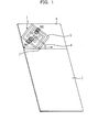
- Fig. 1 illustrates an exemplary structure of an antenna device of an embodiment and a printed board to which the antenna device is fixed;
- Fig. 2A schematically illustrates a plan view of the antenna device illustrated in Fig. 1 ;
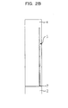
- Fig. 2B schematically illustrates a side view of the antenna device illustrated in Fig. 1 ;
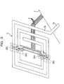
- Fig. 3 illustrates an antenna device of another embodiment
- Fig. 4A illustrates a current density distribution on an antenna device having neither a switch nor a bias line
- Fig. 4B illustrates a current density distribution on an antenna device of a first embodiment
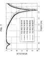
- Fig. 5 is a graph for illustrating a result of simulating an S-parameter (return loss) for signals in a 0.5-6 GHz frequency range in conditions where impedance matching of an antenna device is not achieved;
- Fig. 6A illustrates a result of simulating an S-parameter (return loss) in the 0.5-6 GHz frequency range in conditions where impedance matching of the antenna device of the first embodiment is achieved.
- Fig. 6B illustrates the result illustrated in Fig. 6A by expanding a 0.5-1.1 GHz frequency range.
- Fig. 7 illustrates a result of simulating a return loss in conditions where switches are kept in an unchanged state and an angle ⁇ (an external form of the antenna element) between an antenna element and the printed board illustrated in Fig. 2A is changed.
- An advantage of some aspects of an embodiment of the invention is to provide an antenna device which can occupy a small volume and can change an antenna characteristic.
- An embodiment of the invention is an antenna device including an antenna element having a substantially rectanguiar-shaped planar spiral coil and a switch connected to the antenna element.
- an antenna device which can occupy a small volume and can change an antenna characteristic can be provided.
- Fig. 1 illustrates an externally viewed structure of a wireless communication device having an antenna device.
- Fig. 2A is a plan view of the antenna device illustrated in Fig. 1 .
- Fig. 2B is a side view of the antenna device illustrated in Fig. 1 .
- the antenna device 1 is a planar monopole antenna provided from an end portion of a printed board 2 in one direction of the printed board 2 (a longer side direction of the printed board in Fig. 1 ) and in a direction of the plane of the printed board 2.
- the antenna device 1 is contained in a substrate material 4 having a suitable value of relative permittivity,
- the antenna device 1 is provided in a same direction as the direction of the plane of the printed board 2, so that an effect (mixed noise, etc.) caused by an electronic circuit mounted on the printed board 2 can be reduced.
- the antenna device 1 has an antenna element 5, a plurality (four, e.g., in Figs. 1-3 ) of switches SW1, SW2, SW3, and SW4 (these switches are called, if collectively, “switches SW", hereafter), and a bias line 6 (wiring) which supplies DC currents for driving the switches SW.
- the antenna element 5 has a planar shape as a whole such that a ribbon-like antenna conductor coils into a substantially rectangular-shaped planar spiral coil.
- the substantially rectangular-shaped planar spiral coil is put on one plane.
- the bias line 6 is not illustrated in Fig. 2B in an effort to simplify the drawing.
- the substantially rectangular-shaped planar spiral coil is formed by a plurality of straight portions (antenna arms) 5a-5i. Each of the straight portions from 5b, next to the straight portion 5a, to 5i turns by a certain angle counterclockwise in the drawing, so that the substantially rectangular-shaped planar spiral coil is formed such that the ribbon-like conductor is wound twice.
- the respective straight portions 5a-5i are separated by a certain distance from one another so as to avoid mutual contact. An end of the straight portion 5i is located in the middle of the antenna element 5.
- An end of the straight portion 5a is connected to an RF circuit through a feeding point 7 and an impedance matching circuit mounted on the printed board 2 but not illustrated.
- Directions in which the straight portions 5a and 5d which make a fringe of the antenna element 5 on a side facing the printed board 2 are extended are arranged to in at a certain angle ⁇ for a plane (straight line) which is the end portion of the printed board 2 individually.
- the switches SW1, SW2, SW3, and SW4 are inserted in the middle of the straight portions 5b, 5d, 5f and 5h, respectively, of the antenna element 5 in such a manner as to form a straight line.
- the straight line formed by SW1, SW2, SW3, and SW4 is parallel to straight portion 5a.
- Each one of the switches SW may be comprised of a semiconductor switch, and may be turned on upon being supplied with a dc from the bias line 6.
- the antenna element 5 (antenna arm) changes its length.
- the bias line 6 is located on the back of the antenna element 5 in Fig. 2A .
- the bias line 6 is formed by a first portion 6a located in a direction perpendicular individually to the straight portions 5b, 5d, 5f, and 5h in which the switches SW are inserted.
- a second portion 6b of the bias line 6 extends from the middle of the first portion 6a toward the printed board 2 in a direction perpendicular to the first portion 6a.
- a third portion 6c of the bias line 6 connects an end of the second portion 6b to the printed board 2.
- the third portion 6c crosses the straight portion 5a at an angle of (90 degrees minus ⁇ ).
- the portions of the bias line 6 which overlap the antenna element 5 are located in a direction perpendicular to the respective straight portions of the antenna element 5.
- the antenna element 5 is thereby prevented from getting mixed with noise caused by a current which flows through the bias line 6.
- Fig, 3 illustrates an antenna element 5 of another embodiment.
- the antenna element 5 exemplarily illustrated in Figs. 2A and 2B is provided in such a way as to stand at a certain location within the thickness of the printed board 2.
- the straight portion 5a is integrated with a ribbon-like feeder line 7A which is fixed on one plane of the printed board 2.
- the bias line 6 has lines for supplying on-signals (DC) connected to the respective switches SW and a ground line provided commonly to the switches SW1-SW4.
- the bias line 6 is connected to a control circuit (not illustrated) of the switches SW provided on the printed board 2.
- the switches SW1-SW4 can be individually turned on or off as controlled by the control circuit.
- Figs. 4A and 4B illustrate surface current density distributions on antenna elements radiating a radio wave of 1.5 GHz.
- Fig. 4A illustrates a result of simulating a surface current density distribution on an antenna element provided with neither the bias line 6 nor the switches SW.
- Fig. 4B illustrates a result of simulating a surface current density distribution on the antenna element 5 of the first embodiment provided with the bias line 6 and the switches SW. As illustrated in Fig. 4B , for example, all the switches SW are on.
- the antenna element illustrated in Fig. 4B includes broader portions of higher current density than that illustrated in Fig. 4A .
- the antenna device 1 of the first embodiment has a fine radiation characteristic.
- Fig. 5 is a graph for illustrating a result of simulating an S-parameter (return loss) for signals in a 0.5-6 GHz frequency range in conditions where impedance matching of the antenna device 1 is not achieved.
- Fig. 5 illustrates return losses in cases where all the switches SW1-SW4 are off, all the switches SW1-SW4 are on, the switches SW1-SW3 are on and the switch SW4 is off, the switches SW1 and SW2 are on and the switches SW3 and SW4 are off, and the switch SW 1 is on and the switches SW2-SW4 are off.
- Fig. 6A illustrates a result of simulating an S-parameter (return loss) for signals in the 0.5-6 GHz frequency range in conditions where impedance matching of the antenna device 1 of the first embodiment is achieved.
- Fig. 6B illustrates that result by expanding a 0,5-1.1 GHz frequency range (part A in Fig. 6A ).
- switch positions 1, 2, 3, and 4 correspond to cases where the switch SW1 is on and the switches SW2-SW4 are off, the switches SW1 and SW2 are on and the switches SW3 and SW4 are off, the switches SW1-SW3 are on and the SW4 is off, and the switches SW1-SW4 are on, respectively.
- zones of small return losses are formed in the 0.5-6 GHz frequency range by means of the on-off control of the switches SW1-SW4, and it is thereby known that a wideband antenna which can be preferably used in those frequency bands can be obtained.
- zones of small return losses can be obtained in the respective frequency ranges of 0,62-0.65 GHz, 0.68-0.73 GHz and 0.88-1.03 GHz. It is thereby known that the antenna device 1 can be used also in the 0.6-1.1 GHz frequency range.
- Fig. 7 illustrates a result of simulating a return loss in conditions where the switches SW are kept in an unchanged state and the angle ⁇ (fold angle) between the antenna element 5 and the printed board 2 (see Fig. 2A ) is changed.
- the return losses are measured for the angles ⁇ of 30, 40, 45, 50, and 60 degrees.
- Fig. 7 illustrates an example in a case where the angles ⁇ on the right and left sides in Fig. 2A are equal to each other.
- an interior angle ⁇ 2 of the diamond shape formed by the antenna element 5 in the horizontal direction in Fig. 2A (see Fig. 2A ) is 60 degrees.
- the interior angle 02 80, 90, 100 and 120 degrees, respectively.
- the substantially rectangular-shaped planar spiral coil antenna element 5 is provided with the plural switches SW1-SW4, the antenna element changes its length by means of the on-off operations of the switches SW1-SW4, and the antenna element 5 is consequently in a state of having different antenna characteristics (return loss characteristics). That leads to an antenna device of reconfigurable antenna characteristics.
- An antenna of a small return loss in a desirable frequency band can thereby be obtained by means of the on-off operations of the switches SW1-SW4.
- the antenna device 1 can be used as a wideband antenna which can be applied to that broadband.
- the external form of the antenna element 5 is diamond-shaped (square), the volume occupied by the antenna device 1 can be reduced and, meanwhile, a desirable antenna length can be obtained.
- the external form of the antenna element 5 can be a parallelogram or a rectangle as long as a desirable return loss characteristic can be obtained.
- the angles ⁇ at which the antenna element is fixed to the printed board 2 on the right and left sides with respect to the feeding point 7 ( Fig. 2A ) can be of different values.
- the wiring state of the bias line 6 can be suitably changed as long as a desirable return loss characteristic can be obtained.
- the antenna device 1 is fixed to the printed board 2 on the same plane, the angle at which the antenna device 1 is fixed to the printed board 2 can be suitably set.
Landscapes
- Details Of Aerials (AREA)
- Variable-Direction Aerials And Aerial Arrays (AREA)
Abstract
An antenna device includes an antenna element having an external form shaped into a substantially rectangular-shaped planar spiral coil and a switch provided to the antenna element.
Description
- This application is based upon and claims the benefit of priority of the prior Japanese Patent Application No.
2010-110572, filed on May 12, 2010 - The present invention relates to an antenna device.
- A device for wireless communication is, for example, an electronic apparatus having a wireless communication function. The electronic apparatus may specifically include a wireless terminal such as a mobile phone, a smart phone, a PDA (Personal digital Assistant), a PC (Personal Computer) or a GPS (Global Positioning System) terminal, or a wireless communication application apparatus such as a card for wireless communication (e.g., a PCMCIA card).
- A recent trend in the field of devices for wireless communication is a device for multi-band or wideband wireless communication which uses a plurality of radio frequency bands. Design of such a device for wireless communication, particularly a wireless terminal, is growing more and more complicated year by year, and an antenna element put in the device is desired to be made as small as possible.
- According to an aspect of the embodiment, an antenna device includes an antenna element having an external form shaped into a substantially rectangular-shaped planar spiral coil and a switch coupled to the antenna element.
- The object and advantages of the embodiment will be realized and attained by means of the elements and combinations particularly pointed out in the claims.
- It is to be understood that both the foregoing general description and the following detailed description are exemplary and explanatory and are not restrictive of the embodiment, as claimed.
-
Fig. 1 illustrates an exemplary structure of an antenna device of an embodiment and a printed board to which the antenna device is fixed; -
Fig. 2A schematically illustrates a plan view of the antenna device illustrated inFig. 1 ; -
Fig. 2B schematically illustrates a side view of the antenna device illustrated inFig. 1 ; -
Fig. 3 illustrates an antenna device of another embodiment; -
Fig. 4A illustrates a current density distribution on an antenna device having neither a switch nor a bias line; -
Fig. 4B illustrates a current density distribution on an antenna device of a first embodiment; -
Fig. 5 is a graph for illustrating a result of simulating an S-parameter (return loss) for signals in a 0.5-6 GHz frequency range in conditions where impedance matching of an antenna device is not achieved; -
Fig. 6A illustrates a result of simulating an S-parameter (return loss) in the 0.5-6 GHz frequency range in conditions where impedance matching of the antenna device of the first embodiment is achieved. -
Fig. 6B illustrates the result illustrated inFig. 6A by expanding a 0.5-1.1 GHz frequency range. -
Fig. 7 illustrates a result of simulating a return loss in conditions where switches are kept in an unchanged state and an angle θ (an external form of the antenna element) between an antenna element and the printed board illustrated inFig. 2A is changed. - An advantage of some aspects of an embodiment of the invention is to provide an antenna device which can occupy a small volume and can change an antenna characteristic.
- An embodiment of the invention is an antenna device including an antenna element having a substantially rectanguiar-shaped planar spiral coil and a switch connected to the antenna element.
- According to the embodiment of the invention, an antenna device which can occupy a small volume and can change an antenna characteristic can be provided.
- An embodiment of the invention will be explained with reference to the drawings. A structure of the embodiment described below is exemplary only, and the invention is not limited to the structure of the embodiment.
-
Fig. 1 illustrates an externally viewed structure of a wireless communication device having an antenna device.Fig. 2A is a plan view of the antenna device illustrated inFig. 1 .Fig. 2B is a side view of the antenna device illustrated inFig. 1 . - As illustrated in
Fig. 1 , theantenna device 1 is a planar monopole antenna provided from an end portion of a printedboard 2 in one direction of the printed board 2 (a longer side direction of the printed board inFig. 1 ) and in a direction of the plane of the printedboard 2. Theantenna device 1 is contained in asubstrate material 4 having a suitable value of relative permittivity, Theantenna device 1 is provided in a same direction as the direction of the plane of the printedboard 2, so that an effect (mixed noise, etc.) caused by an electronic circuit mounted on the printedboard 2 can be reduced. - As illustrated in
Figs. 2A ,2B , and3 , theantenna device 1 has anantenna element 5, a plurality (four, e.g., inFigs. 1-3 ) of switches SW1, SW2, SW3, and SW4 (these switches are called, if collectively, "switches SW", hereafter), and a bias line 6 (wiring) which supplies DC currents for driving the switches SW. - As illustrated in
Fig. 2A , theantenna element 5 has a planar shape as a whole such that a ribbon-like antenna conductor coils into a substantially rectangular-shaped planar spiral coil. As illustrated inFig. 2B , the substantially rectangular-shaped planar spiral coil is put on one plane. Incidentally, thebias line 6 is not illustrated inFig. 2B in an effort to simplify the drawing. The substantially rectangular-shaped planar spiral coil is formed by a plurality of straight portions (antenna arms) 5a-5i. Each of the straight portions from 5b, next to thestraight portion 5a, to 5i turns by a certain angle counterclockwise in the drawing, so that the substantially rectangular-shaped planar spiral coil is formed such that the ribbon-like conductor is wound twice. The respectivestraight portions 5a-5i are separated by a certain distance from one another so as to avoid mutual contact. An end of the straight portion 5i is located in the middle of theantenna element 5. - An end of the
straight portion 5a is connected to an RF circuit through afeeding point 7 and an impedance matching circuit mounted on the printedboard 2 but not illustrated. Directions in which thestraight portions 5a and 5d which make a fringe of theantenna element 5 on a side facing the printedboard 2 are extended (the direction in which thestraight portion 5a is extended (from lower left to upper right) and the direction in which the straight portion 5d is extended (from lower right to upper left) inFig. 2A ) are arranged to in at a certain angle θ for a plane (straight line) which is the end portion of the printedboard 2 individually. - The switches SW1, SW2, SW3, and SW4 are inserted in the middle of the
straight portions antenna element 5 in such a manner as to form a straight line. As illustrated inFig. 2A , the straight line formed by SW1, SW2, SW3, and SW4 is parallel tostraight portion 5a. Each one of the switches SW may be comprised of a semiconductor switch, and may be turned on upon being supplied with a dc from thebias line 6. Upon the switches SW1-SW4 being turned on, the antenna element 5 (antenna arm) changes its length. - The
bias line 6 is located on the back of theantenna element 5 inFig. 2A . Thebias line 6 is formed by a first portion 6a located in a direction perpendicular individually to thestraight portions second portion 6b of thebias line 6 extends from the middle of the first portion 6a toward the printedboard 2 in a direction perpendicular to the first portion 6a. A third portion 6c of thebias line 6 connects an end of thesecond portion 6b to the printedboard 2. The third portion 6c crosses thestraight portion 5a at an angle of (90 degrees minus θ). As describes above, the portions of thebias line 6 which overlap theantenna element 5 are located in a direction perpendicular to the respective straight portions of theantenna element 5. Theantenna element 5 is thereby prevented from getting mixed with noise caused by a current which flows through thebias line 6. -
Fig, 3 illustrates anantenna element 5 of another embodiment. Theantenna element 5 exemplarily illustrated inFigs. 2A and2B is provided in such a way as to stand at a certain location within the thickness of the printedboard 2. As exemplarily illustrated inFig. 3 , meanwhile, thestraight portion 5a is integrated with a ribbon-like feeder line 7A which is fixed on one plane of the printedboard 2. - The
bias line 6 has lines for supplying on-signals (DC) connected to the respective switches SW and a ground line provided commonly to the switches SW1-SW4. Thebias line 6 is connected to a control circuit (not illustrated) of the switches SW provided on the printedboard 2. The switches SW1-SW4 can be individually turned on or off as controlled by the control circuit. -
Figs. 4A and4B illustrate surface current density distributions on antenna elements radiating a radio wave of 1.5 GHz.Fig. 4A illustrates a result of simulating a surface current density distribution on an antenna element provided with neither thebias line 6 nor the switches SW.Fig. 4B illustrates a result of simulating a surface current density distribution on theantenna element 5 of the first embodiment provided with thebias line 6 and the switches SW. As illustrated inFig. 4B , for example, all the switches SW are on. As illustrated inFigs. 4A and4B , the antenna element illustrated inFig. 4B includes broader portions of higher current density than that illustrated inFig. 4A . Theantenna device 1 of the first embodiment has a fine radiation characteristic. -
Fig. 5 is a graph for illustrating a result of simulating an S-parameter (return loss) for signals in a 0.5-6 GHz frequency range in conditions where impedance matching of theantenna device 1 is not achieved.Fig. 5 illustrates return losses in cases where all the switches SW1-SW4 are off, all the switches SW1-SW4 are on, the switches SW1-SW3 are on and the switch SW4 is off, the switches SW1 and SW2 are on and the switches SW3 and SW4 are off, and theswitch SW 1 is on and the switches SW2-SW4 are off. -
Fig. 6A illustrates a result of simulating an S-parameter (return loss) for signals in the 0.5-6 GHz frequency range in conditions where impedance matching of theantenna device 1 of the first embodiment is achieved.Fig. 6B illustrates that result by expanding a 0,5-1.1 GHz frequency range (part A inFig. 6A ). A matching circuit formed by an inductor (L) and a capacitor (C) for the simulation is applied for impedance matching, where the values L and C are set in the ranges of L= 1-10 nH and C=0.25-6 pF. - In
Figs. 6A and6B ,switch positions - As illustrated in
Fig. 6A , zones of small return losses are formed in the 0.5-6 GHz frequency range by means of the on-off control of the switches SW1-SW4, and it is thereby known that a wideband antenna which can be preferably used in those frequency bands can be obtained. As illustrated inFig. 6B , it is further known that zones of small return losses can be obtained in the respective frequency ranges of 0,62-0.65 GHz, 0.68-0.73 GHz and 0.88-1.03 GHz. It is thereby known that theantenna device 1 can be used also in the 0.6-1.1 GHz frequency range. -
Fig. 7 illustrates a result of simulating a return loss in conditions where the switches SW are kept in an unchanged state and the angle θ (fold angle) between theantenna element 5 and the printed board 2 (seeFig. 2A ) is changed. As illustrated inFig. 7 , the return losses are measured for the angles θ of 30, 40, 45, 50, and 60 degrees.Fig. 7 illustrates an example in a case where the angles θ on the right and left sides inFig. 2A are equal to each other. Incidentally, when θ=30 degrees, an interior angle θ2 of the diamond shape formed by theantenna element 5 in the horizontal direction inFig. 2A (seeFig. 2A ) is 60 degrees. When θ=40, 45, 50 and 60 degrees, the interior angle 02=80, 90, 100 and 120 degrees, respectively. When θ=45 degrees, the external form of theantenna element 5 is a square. - As the results illustrated in
Fig. 7 demonstrate, theantenna device 1 can have acceptable return losses for use for the respective values in the range of θ=30-60 degrees. The lowest return loss is obtained, in particular, when θ=45 degrees. It is known that the external form of theantenna element 5 should preferably be a square, i.e., θ=45 degrees. For θ=50 or 60 degrees, meanwhile, theantenna element 5 grows longer in the direction of height (top to bottom direction inFig. 2A ) and grows larger in terms of the volume occupied by the antenna device 1 (grows longer in the longer side direction in combination with the printed board 2). It is thereby known that the condition of θ=45 degrees is most preferable in the above result from viewpoints of the return loss and the size of the antenna element. - According to the above embodiments, the substantially rectangular-shaped planar spiral
coil antenna element 5 is provided with the plural switches SW1-SW4, the antenna element changes its length by means of the on-off operations of the switches SW1-SW4, and theantenna element 5 is consequently in a state of having different antenna characteristics (return loss characteristics). That leads to an antenna device of reconfigurable antenna characteristics. An antenna of a small return loss in a desirable frequency band can thereby be obtained by means of the on-off operations of the switches SW1-SW4. As the zones of small return losses span the broadband of 0,6-6 GHz, theantenna device 1 can be used as a wideband antenna which can be applied to that broadband. - Further, as the external form of the
antenna element 5 is diamond-shaped (square), the volume occupied by theantenna device 1 can be reduced and, meanwhile, a desirable antenna length can be obtained. Incidentally, the external form of theantenna element 5 can be a parallelogram or a rectangle as long as a desirable return loss characteristic can be obtained. Further, the angles θ at which the antenna element is fixed to the printedboard 2 on the right and left sides with respect to the feeding point 7 (Fig. 2A ) can be of different values. Further, the wiring state of thebias line 6 can be suitably changed as long as a desirable return loss characteristic can be obtained. Further, although theantenna device 1 is fixed to the printedboard 2 on the same plane, the angle at which theantenna device 1 is fixed to the printedboard 2 can be suitably set. - All examples and conditional language recited herein are intended for pedagogical purposes to aid the reader in understanding the principles of the invention and the concepts contributed by the inventor to furthering the art, and are to be construed as being without limitation to such specifically recited examples and conditions, nor does the organization of such examples in the specification relate to a showing of the superiority and inferiority of the invention. Although the embodiments of the present invention have been described in detail, it should be understood that the various changes, substitutions, and alterations could be made hereto without departing from the spirit and scope of the invention.
Claims (5)
- An antenna device comprising:an antenna element having an external form shaped into a substantially rectangular-shaped planar spiral coil ; anda first switch coupled to the antenna element,
- The antenna device according to Claim 1, wherein:the antenna element has a first end located on a vertex of the rectangular-shaped planar spiral coil and a second end located on a middle portion of the antenna element; andthe first end of the antenna element is fixed to a printed board in such a way that each of two portions of the antenna element located individually on two sides including the vertex crosses a straight fringe of the printed board at an angle θ.
- The antenna device according to Claim 2, wherein the angle θ is between 30 and 60 degrees.
- The antenna device according to Claim 1, further comprising extra second switch which can be turned on or off separately from the first switch.
- The antenna device according to Claim 1, further comprising a line which supplies the first switch with an on-off signal, the line being located in a direction perpendicular to a straight portion of the antenna element.
Applications Claiming Priority (1)
| Application Number | Priority Date | Filing Date | Title |
|---|---|---|---|
| JP2010110572A JP2011239302A (en) | 2010-05-12 | 2010-05-12 | Antenna device |
Publications (1)
| Publication Number | Publication Date |
|---|---|
| EP2387110A1 true EP2387110A1 (en) | 2011-11-16 |
Family
ID=44244706
Family Applications (1)
| Application Number | Title | Priority Date | Filing Date |
|---|---|---|---|
| EP11162590A Withdrawn EP2387110A1 (en) | 2010-05-12 | 2011-04-15 | Antenna device |
Country Status (3)
| Country | Link |
|---|---|
| US (1) | US20110279348A1 (en) |
| EP (1) | EP2387110A1 (en) |
| JP (1) | JP2011239302A (en) |
Cited By (1)
| Publication number | Priority date | Publication date | Assignee | Title |
|---|---|---|---|---|
| EP3054527A4 (en) * | 2013-10-04 | 2017-05-10 | Samsung Electronics Co., Ltd. | Antenna device of electronic apparatus |
Families Citing this family (4)
| Publication number | Priority date | Publication date | Assignee | Title |
|---|---|---|---|---|
| US8776002B2 (en) * | 2011-09-06 | 2014-07-08 | Variable Z0, Ltd. | Variable Z0 antenna device design system and method |
| CN104466409B (en) * | 2014-12-05 | 2017-10-24 | 广东欧珀移动通信有限公司 | Antenna structure and the mobile terminal with the antenna structure |
| USD812598S1 (en) * | 2015-06-17 | 2018-03-13 | Inside Secure | Data communication antenna |
| CN113765528B (en) * | 2021-07-23 | 2022-10-14 | 上海闻泰信息技术有限公司 | Reconfigurable antenna, electronic device, and tuning control method |
Citations (5)
| Publication number | Priority date | Publication date | Assignee | Title |
|---|---|---|---|---|
| WO2005062421A1 (en) * | 2003-12-24 | 2005-07-07 | Wivenhoe Technology Limited | An antenna having controllable direction of radiation |
| US20070229376A1 (en) * | 2006-04-03 | 2007-10-04 | Ethertronics | Antenna configured for low frequency applications |
| GB2450786A (en) * | 2007-07-03 | 2009-01-07 | Antenova Ltd | Antenna module with adjustable beam and polarization characterisitcs |
| US20090156191A1 (en) * | 2007-12-14 | 2009-06-18 | Microsoft Corporation | Computing device with configurable antenna |
| JP2010110572A (en) | 2008-11-10 | 2010-05-20 | Top Corp | Three-way cock |
Family Cites Families (5)
| Publication number | Priority date | Publication date | Assignee | Title |
|---|---|---|---|---|
| EP1929320A2 (en) * | 2004-09-16 | 2008-06-11 | Koninklijke Philips Electronics N.V. | Magnetic resonance receive coils with compact inductive components |
| US7692602B2 (en) * | 2006-02-06 | 2010-04-06 | G-Time Electronic Co., Ltd. | Control system of antenna array of RFID reader applications |
| US8463332B2 (en) * | 2006-08-31 | 2013-06-11 | Semiconductor Energy Laboratory Co., Ltd. | Wireless communication device |
| US20110187533A1 (en) * | 2007-08-13 | 2011-08-04 | Mti Wireless Edge Ltd. | Antenna for Near Field Radio-Frequency Identification and Method and System for Use Thereof |
| US7936237B2 (en) * | 2008-11-04 | 2011-05-03 | Redpine Signals, Inc. | Multi-band transmit-receive switch for wireless transceiver |
-
2010
- 2010-05-12 JP JP2010110572A patent/JP2011239302A/en not_active Withdrawn
-
2011
- 2011-03-31 US US13/076,710 patent/US20110279348A1/en not_active Abandoned
- 2011-04-15 EP EP11162590A patent/EP2387110A1/en not_active Withdrawn
Patent Citations (5)
| Publication number | Priority date | Publication date | Assignee | Title |
|---|---|---|---|---|
| WO2005062421A1 (en) * | 2003-12-24 | 2005-07-07 | Wivenhoe Technology Limited | An antenna having controllable direction of radiation |
| US20070229376A1 (en) * | 2006-04-03 | 2007-10-04 | Ethertronics | Antenna configured for low frequency applications |
| GB2450786A (en) * | 2007-07-03 | 2009-01-07 | Antenova Ltd | Antenna module with adjustable beam and polarization characterisitcs |
| US20090156191A1 (en) * | 2007-12-14 | 2009-06-18 | Microsoft Corporation | Computing device with configurable antenna |
| JP2010110572A (en) | 2008-11-10 | 2010-05-20 | Top Corp | Three-way cock |
Cited By (2)
| Publication number | Priority date | Publication date | Assignee | Title |
|---|---|---|---|---|
| EP3054527A4 (en) * | 2013-10-04 | 2017-05-10 | Samsung Electronics Co., Ltd. | Antenna device of electronic apparatus |
| US10063285B2 (en) | 2013-10-04 | 2018-08-28 | Samsung Electronics Co., Ltd. | Antenna device of electronic apparatus |
Also Published As
| Publication number | Publication date |
|---|---|
| US20110279348A1 (en) | 2011-11-17 |
| JP2011239302A (en) | 2011-11-24 |
Similar Documents
| Publication | Publication Date | Title |
|---|---|---|
| US7903034B2 (en) | Antenna set, portable wireless device, and use of a conductive element for tuning the ground-plane of the antenna set | |
| EP1869726B1 (en) | An antenna having a plurality of resonant frequencies | |
| KR100638621B1 (en) | Broadband internal antenna | |
| US7990320B2 (en) | Antenna with inner spring contact | |
| US20190006761A1 (en) | Antenna for a portable computer | |
| EP2418728A1 (en) | Antenna arrangement, dielectric substrate, PCB & device | |
| JP2006196994A (en) | Wireless device | |
| WO2004112189A1 (en) | A multiband antenna for a portable terminal apparatus | |
| JP5998974B2 (en) | antenna | |
| JP4233100B2 (en) | Wireless device | |
| US10014574B2 (en) | Antenna device | |
| EP2387110A1 (en) | Antenna device | |
| JP2009111959A (en) | Parallel 2-wire antenna and wireless communication device | |
| US20050237255A1 (en) | Small footprint dual band dipole antennas for wireless networking | |
| US7495617B2 (en) | Multi-band antenna | |
| KR100756312B1 (en) | Multiband internal antenna with adjustable resonant frequency and input impedance | |
| TWI536666B (en) | Antenna | |
| US20070171128A1 (en) | Planar antenna with short-trace | |
| JP2010130100A (en) | Multiband antenna apparatus | |
| JP4473825B2 (en) | Mobile terminal antenna | |
| JP2012065218A (en) | Portable communication apparatus | |
| JP6489153B2 (en) | Antenna device | |
| Syrytsin et al. | Pattern-reconfigurable mobile terminal antenna system for MIMO and link stabilization in LTE | |
| KR20080045876A (en) | Spiral antenna with dual radiator structure | |
| SE515314C2 (en) | Antenna arrangement for handheld portable radio communication device, has microstrip element provided with opening to allow radiation from whip element |
Legal Events
| Date | Code | Title | Description |
|---|---|---|---|
| AK | Designated contracting states |
Kind code of ref document: A1 Designated state(s): AL AT BE BG CH CY CZ DE DK EE ES FI FR GB GR HR HU IE IS IT LI LT LU LV MC MK MT NL NO PL PT RO RS SE SI SK SM TR |
|
| AX | Request for extension of the european patent |
Extension state: BA ME |
|
| PUAI | Public reference made under article 153(3) epc to a published international application that has entered the european phase |
Free format text: ORIGINAL CODE: 0009012 |
|
| STAA | Information on the status of an ep patent application or granted ep patent |
Free format text: STATUS: THE APPLICATION IS DEEMED TO BE WITHDRAWN |
|
| 18D | Application deemed to be withdrawn |
Effective date: 20120517 |