EP2386620A1 - Chloride scintillator for radiation detection - Google Patents
Chloride scintillator for radiation detection Download PDFInfo
- Publication number
- EP2386620A1 EP2386620A1 EP11165489A EP11165489A EP2386620A1 EP 2386620 A1 EP2386620 A1 EP 2386620A1 EP 11165489 A EP11165489 A EP 11165489A EP 11165489 A EP11165489 A EP 11165489A EP 2386620 A1 EP2386620 A1 EP 2386620A1
- Authority
- EP
- European Patent Office
- Prior art keywords
- scintillator material
- consists essentially
- combination
- formula
- radiation
- Prior art date
- Legal status (The legal status is an assumption and is not a legal conclusion. Google has not performed a legal analysis and makes no representation as to the accuracy of the status listed.)
- Granted
Links
Images







Classifications
-
- G—PHYSICS
- G21—NUCLEAR PHYSICS; NUCLEAR ENGINEERING
- G21K—HANDLING OF PARTICLES OR IONISING RADIATION NOT OTHERWISE PROVIDED FOR; IRRADIATION DEVICES; GAMMA RAY OR X-RAY MICROSCOPES
- G21K4/00—Conversion screens for the conversion of the spatial distribution of X-rays or particle radiation into visible images, e.g. fluoroscopic screens
-
- C—CHEMISTRY; METALLURGY
- C09—DYES; PAINTS; POLISHES; NATURAL RESINS; ADHESIVES; COMPOSITIONS NOT OTHERWISE PROVIDED FOR; APPLICATIONS OF MATERIALS NOT OTHERWISE PROVIDED FOR
- C09K—MATERIALS FOR MISCELLANEOUS APPLICATIONS, NOT PROVIDED FOR ELSEWHERE
- C09K11/00—Luminescent materials, e.g. electroluminescent or chemiluminescent
- C09K11/08—Luminescent materials, e.g. electroluminescent or chemiluminescent containing inorganic luminescent materials
- C09K11/77—Luminescent materials, e.g. electroluminescent or chemiluminescent containing inorganic luminescent materials containing rare earth metals
- C09K11/7704—Halogenides
- C09K11/7705—Halogenides with alkali or alkaline earth metals
-
- C—CHEMISTRY; METALLURGY
- C09—DYES; PAINTS; POLISHES; NATURAL RESINS; ADHESIVES; COMPOSITIONS NOT OTHERWISE PROVIDED FOR; APPLICATIONS OF MATERIALS NOT OTHERWISE PROVIDED FOR
- C09K—MATERIALS FOR MISCELLANEOUS APPLICATIONS, NOT PROVIDED FOR ELSEWHERE
- C09K11/00—Luminescent materials, e.g. electroluminescent or chemiluminescent
- C09K11/08—Luminescent materials, e.g. electroluminescent or chemiluminescent containing inorganic luminescent materials
- C09K11/77—Luminescent materials, e.g. electroluminescent or chemiluminescent containing inorganic luminescent materials containing rare earth metals
- C09K11/7715—Luminescent materials, e.g. electroluminescent or chemiluminescent containing inorganic luminescent materials containing rare earth metals containing cerium
- C09K11/7719—Halogenides
- C09K11/772—Halogenides with alkali or alkaline earth metals
-
- C—CHEMISTRY; METALLURGY
- C09—DYES; PAINTS; POLISHES; NATURAL RESINS; ADHESIVES; COMPOSITIONS NOT OTHERWISE PROVIDED FOR; APPLICATIONS OF MATERIALS NOT OTHERWISE PROVIDED FOR
- C09K—MATERIALS FOR MISCELLANEOUS APPLICATIONS, NOT PROVIDED FOR ELSEWHERE
- C09K11/00—Luminescent materials, e.g. electroluminescent or chemiluminescent
- C09K11/08—Luminescent materials, e.g. electroluminescent or chemiluminescent containing inorganic luminescent materials
- C09K11/77—Luminescent materials, e.g. electroluminescent or chemiluminescent containing inorganic luminescent materials containing rare earth metals
- C09K11/7766—Luminescent materials, e.g. electroluminescent or chemiluminescent containing inorganic luminescent materials containing rare earth metals containing two or more rare earth metals
- C09K11/7772—Halogenides
- C09K11/7773—Halogenides with alkali or alkaline earth metal
-
- C—CHEMISTRY; METALLURGY
- C30—CRYSTAL GROWTH
- C30B—SINGLE-CRYSTAL GROWTH; UNIDIRECTIONAL SOLIDIFICATION OF EUTECTIC MATERIAL OR UNIDIRECTIONAL DEMIXING OF EUTECTOID MATERIAL; REFINING BY ZONE-MELTING OF MATERIAL; PRODUCTION OF A HOMOGENEOUS POLYCRYSTALLINE MATERIAL WITH DEFINED STRUCTURE; SINGLE CRYSTALS OR HOMOGENEOUS POLYCRYSTALLINE MATERIAL WITH DEFINED STRUCTURE; AFTER-TREATMENT OF SINGLE CRYSTALS OR A HOMOGENEOUS POLYCRYSTALLINE MATERIAL WITH DEFINED STRUCTURE; APPARATUS THEREFOR
- C30B11/00—Single-crystal growth by normal freezing or freezing under temperature gradient, e.g. Bridgman-Stockbarger method
-
- C—CHEMISTRY; METALLURGY
- C30—CRYSTAL GROWTH
- C30B—SINGLE-CRYSTAL GROWTH; UNIDIRECTIONAL SOLIDIFICATION OF EUTECTIC MATERIAL OR UNIDIRECTIONAL DEMIXING OF EUTECTOID MATERIAL; REFINING BY ZONE-MELTING OF MATERIAL; PRODUCTION OF A HOMOGENEOUS POLYCRYSTALLINE MATERIAL WITH DEFINED STRUCTURE; SINGLE CRYSTALS OR HOMOGENEOUS POLYCRYSTALLINE MATERIAL WITH DEFINED STRUCTURE; AFTER-TREATMENT OF SINGLE CRYSTALS OR A HOMOGENEOUS POLYCRYSTALLINE MATERIAL WITH DEFINED STRUCTURE; APPARATUS THEREFOR
- C30B29/00—Single crystals or homogeneous polycrystalline material with defined structure characterised by the material or by their shape
- C30B29/10—Inorganic compounds or compositions
- C30B29/12—Halides
-
- G—PHYSICS
- G21—NUCLEAR PHYSICS; NUCLEAR ENGINEERING
- G21K—HANDLING OF PARTICLES OR IONISING RADIATION NOT OTHERWISE PROVIDED FOR; IRRADIATION DEVICES; GAMMA RAY OR X-RAY MICROSCOPES
- G21K4/00—Conversion screens for the conversion of the spatial distribution of X-rays or particle radiation into visible images, e.g. fluoroscopic screens
- G21K2004/06—Conversion screens for the conversion of the spatial distribution of X-rays or particle radiation into visible images, e.g. fluoroscopic screens with a phosphor layer
Definitions
- Fig. 2 shows a single crystal of Ce-doped KGdCl 7 (KGd 2 ( 1- x )Ce 2 x ,Cl 7 ) made according to one aspect of the present disclosure.
- Fig. 5(a) shows a scintillation decay time spectrum of a Cs 3 CeCl 6 crystal; the spectrum was measured using 137 Cs gamma-ray source (662 keV).
- Fig. 9 shows a scintillation decay time spectrum of a Cs 3 CeCl 6 single crystal; the spectrum was measured using 137 Cs gamma-ray source (662 keV).
- a method of growing a scintillator crystal described above includes synthesizing a compound of the composition discussed above and then growing a scintillator crystal from the synthesized compound.
- the synthesized compound is sealed in a quartz ampoule, which is pulled
- certain single crystals with a combination of Gd and Ce can be effective in thermal neutron detection due to the large cross-section for thermal neutron absorption for Gd isotopes, in particular 157 Gd and 155 Gd.
- effective thermal neutron detection was observed for KGd 2 Cl 7 and CsGd 2 Cl 7 .
Landscapes
- Chemical & Material Sciences (AREA)
- Engineering & Computer Science (AREA)
- Materials Engineering (AREA)
- Organic Chemistry (AREA)
- Inorganic Chemistry (AREA)
- Metallurgy (AREA)
- Crystallography & Structural Chemistry (AREA)
- Physics & Mathematics (AREA)
- General Engineering & Computer Science (AREA)
- High Energy & Nuclear Physics (AREA)
- Luminescent Compositions (AREA)
- Crystals, And After-Treatments Of Crystals (AREA)
- Measurement Of Radiation (AREA)
Abstract
Description
- The present application claims the benefit of
U.S. Provisional Application Serial No. 61/332,972, filed May 10, 2010 U.S. Provisional Application Serial No. 61/332,945, filed May 10, 2010 U.S. Provisional Application Serial No. 61/332,934, filed May 10, 2010 - This disclosure relates to scintillator materials used for detecting ionizing radiation, such as X-rays, gamma rays and thermal neutron radiation, in security, medical imaging, particle physics and other applications. This disclosure relates particularly to chloride scintillator materials. Certain arrangements also relate to specific compositions of such scintillator material, method of making the same and devices with such scintillator materials as components.
- Scintillator materials, which emit light pulses in response to impinging radiation, such as X-rays, gamma rays and thermal neutron radiation, are used in detectors that have a wide range of applications in medical imaging, particle physics, geological exploration, security and other related areas. Considerations in selecting scintillator materials typically include, but are not limited to, luminosity, decay time and emission wavelengths.
- While a variety of scintillator materials have been made, there is a continuous need for superior scintillator materials.
- The present disclosure relates generally to chloride scintillator materials and method of making such scintillator materials. In one arrangement, a chloride scintillator material is single-crystalline and has a composition of the formula A3MC16, wherein A consists essentially of Li, Na K, Rb, Cs or any combination thereof, and M consists essentially of Ce, Sc, Y, La, Lu, Gd, Pr, Tb, Yb, Nd or any combination thereof. In another arrangement, a chloride scintillator material is single-crystalline and has a composition of the formula AM2Cl7, wherein A consists essentially of Li, Na K, Rb, Cs or any combination thereof, and M consists essentially of Ce, Sc, Y, La, Lu, Gd, Pr, Tb, Yb, Nd or any combination thereof. Specific examples of these scintillator materials include single-crystalline CS3CeCl6, CsCe2Cl7, Ce-doped KGd2Cl7 (KGd2(1-x )Ce2x Cl7) and Ce-doped CsGd2Cl7 (CsGd2(1-x )Ce2x Cl7).
- A further aspect of the present disclosure relates to a method of making chloride scintillator materials of the above-mentioned compositions. In one example, high-purity starting chlorides (such as CsCl and CeCl3) are mixed and melted to synthesize a compound of the desired composition of the scintillator material. A single crystal of the scintillator material is then grown from the synthesized compound by the Bridgman method, in which a sealed ampoule containing the synthesized compound is transported from a hot zone to a cold zone through a controlled temperature gradient at a controlled speed to form a single-crystalline scintillator from molten synthesized compound.
-
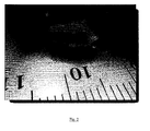
Fig. 1 shows a single crystal of Cs3CeCl6 made according to one aspect of the present disclosure. -
Fig. 2 shows a single crystal of Ce-doped KGdCl7 (KGd2(1-x )Ce2x ,Cl7) made according to one aspect of the present disclosure. -
Fig. 3 shows a single crystal of CsCe2Cl7 (upper) and a single crystal of Cs3CeCl6 (lower) made according to one aspect of the present disclosure. The images were taken with the samples under ultraviolet excitation. -
Fig. 4 shows a power X-ray diffraction pattern (upper spectrum) of a Cs3CeCl6 crystal sample; the material is identified as a single phase from the PCPDF database, Ref. No. 00-038-1315 (lower spectrum). -
Fig. 5(a) shows a scintillation decay time spectrum of a Cs3CeCl6 crystal; the spectrum was measured using 137Cs gamma-ray source (662 keV). -
Fig. 5(b) shows a scintillation decay time spectrum of a KGd2Cl7:Ce 1% (KGd2(1-x)Ce2x Cl7, x=0.01) crystal; the spectrum was measured using 137Cs gamma-ray source (662 keV). -
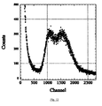
Fig. 6 shows an energy spectrum of a Cs3CeCl6 crystal, indicating a photopeak at about channel no. 300 (normalized, with the photopeak of a BGO standard sample at channel no. 100); the spectrum was measured using 137Cs gamma-ray source (662 keV). -
Fig. 7 shows radioluminescence spectra of Cs3CeCl6 and CsCe2Cl7 single crystals under the excitation of X-rays. -
Fig. 8 shows a scintillation decay time spectrum of a CsCe2Cl7 single crystal; the spectrum was measured using 137Cs gamma-ray source (662 keV). -
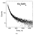
Fig. 9 shows a scintillation decay time spectrum of a Cs3CeCl6 single crystal; the spectrum was measured using 137Cs gamma-ray source (662 keV). -
Fig. 10 shows energy spectra of Cs3CeCl6 and CsCe2Cl7 single crystals as compared to that of a BGO reference sample; the spectrum was measured using 137Cs gamma-ray source (662 keV). -
Fig. 11 shows an energy spectrum of a KGd2Cl7:Ce (KGd2(1-x )Ce2x Cl7, x=0.01) 1% crystal, indicating a photopeak at about channel no. 400 (normalized, with the photopeak of a BGO standard sample at channel no. 100); the spectrum was measured using 137Cs gamma-ray source (662 keV). -
Fig. 12 shows an energy spectrum ofKGd2Cl7:Ce 1% (KGd2(1-x )Ce2x Cl7, x=0.01) showing 33 and 77 keV peaks, characteristic for thermal neutron interaction with Gd; measured using a 252Cf thermal neutron source. The sample was shielded from the gamma-rays. -
Fig. 13 shows an energy spectrum of a KGd2Cl7:Ce 1% (KGd2(1-x)Ce2x Cl7, x=0.01) crystal, showing peaks at about 34 and 74 keV; the spectrum was measured using 252Cf neutron source, with the sample shielded from gamma rays. -
Fig. 14 shows emission and excitation spectra of KGd2Cl7:Ce 3at% (KGd2(1-x)Ce2x Cl7, x=0.03) and CsGd2Cl7:Ce 3at% (CsGd2(1-x )Ce2x Cl7, x=0.03). The excitation spectra were taken at an excitation wavelength of 265 nm; the emission spectra were taken at an emission wavelength of 395 nm. -
Fig. 15 shows radioluminescence spectra KGd2Cl7:Ce 3at% (KGd2(1-x)Ce2x Cl7, x=0.03) and CsGd2Cl7:Ce 3at%. -
Fig. 16 shows scintillation decay time spectra of KGd2Cl7:Ce 3% (KGd2(1-x )Ce2x Cl7, x=0.03) and CsGd2Cl7:Ce 3% (CsGd2(1-x )Ce2x Cl7, x=0.03) single crystals; the spectra were measured using 137Cs gamma-ray source (662 keV). -
Fig. 17 shows energy spectra of KGd2Cl7:Ce 3% (KGd2(1-x )Ce2x Cl7, x=0.03) and CsGd2Cl7:Ce 3% (CsGd2(1-x )Ce2x Cl7, x=0.03) as compared to that of a BGO reference sample; the spectrum was measured using 137Cs gamma-ray source (662 keV). -
Fig. 18 shows an energy spectrum of CsGd2Cl7:Ce 3% (CsGd2(1-x)Ce2x Cl7, x=0.03) single crystal under neuron excitation. - Inorganic scintillators are commonly used in nuclear and high-energy physics research, medical imaging, homeland security, and geological exploration. These materials typically possess sufficient stopping power for detection, high luminosity, high spectral energy resolution at room temperature and short decay time. Certain cerium-doped halides, such as LaCl3:Ce and LaBr3:Ce, have satisfactory scintillation properties at room temperature for gamma ray detection. Another desirable property of scintillators is a capability of neutron-gamma discrimination that is of importance for nuclear non-proliferation applications. Materials containing gadolinium, lithium and boron are employed to quickly and efficiently discriminate neutrons from gamma rays. Halide scintillators reported to date are produced mainly by the conventional Bridgman crystal growth method.
- In one aspect of present disclosure, a chloride scintillator material is a single-crystalline material and has a composition of the formula A3MCl6, wherein A consists essentially of Li, Na, K, Rb, Cs or any combination thereof, and M consists essentially of Ce, Sc, Y, La, Lu, Gd, Pr, Tb, Yb, Nd or any combination thereof. In another aspect, a chloride scintillator material is a single-crystalline material and has a composition of the formula AM2Cl7, wherein A consists essentially of Li, Na K, Rb, Cs or any combination thereof, and M consists essentially of Ce, Sc , Y, La, Lu, Gd, Pr, Tb, Yb, Nd or any combination thereof. Specific examples of these scintillator materials include single-crystalline Cs3CeCl6, CsCe2Cl7, Ce-doped KGd2Cl7 (KGd2(1-x )Ce2 xCl7 and Ce-doped CsGd2Cl7 (CsGd2(1-x )Ce2x Cl7).
- Cs3CeCl6 and CsCe2Cl7 are congruently melting compounds that exist in CsCl-CeCl3 system. This fact makes Cs3CeCl6 and CsCe2Cl7 suitable for practical crystal growth from a melt. Cs3CeCl6 has a density of 3.4 g/cm3, melts congruently at 804°C and undergoes a solid-solid state transition at 401°C. Its high-temperature modification crystallizes in the cubic elpasolite type and a low-temperature modification in a monoclinic crystal structure. CsCe2Cl7 has a density of 3.6 g/cm3 and a hexagonal crystal structure KGd2Cl7 has an monoclinic crystal structure and melts congruently at 573°C. CsGd2Cl7 have a orthorhombic crystal structure and melts congruently at 680°C. Therefore they both can be grown from the melt.
- In one aspect of the present disclosure, a method of growing a scintillator crystal described above includes synthesizing a compound of the composition discussed above and then growing a scintillator crystal from the synthesized compound. In one example, the synthesized compound is sealed in a quartz ampoule, which is pulled
- In another aspect of the present disclosure, the above-described scintillator materials are used in radiation detection by scintillation. For example, a radiation detector can include a scintillator described above for generating photons in response to the impinging radiation. The scintillator is optically coupled to a photon detector, such as a photomultiplier tube (PMT), arranged to receive the photons generated by the scintillator and adapted to generate a signal indicative of the photon generation.
- In one arrangement, a modified 24-zone Electro-Dynamic Gradient Mellen furnace with a translation mechanism was used to grow CS3CeCl6 and CsCe2Cl7 single crystals via the Bridgman technique. As a first step, these compounds were synthesized by mixing and melting starting anhydrous chlorides in quartz ampoules. Quartz ampoules were first baked and freshly cleaned by rinsing with a dilute HF solution and deionized water. High purity, anhydrous beads of starting compounds (e.g., CsCl and CeCl3 for Cs3CeCl6 and CsCe2Cl7; KCl and GdCl3 for KGd2Cl7 and CsCl and GdCl3 for CsGd2Cl7) (available from Sigma-Aldrich)) were loaded into the cylindrical quartz ampoules in a nitrogen-purged glove box and sealed under 10-6 mbar vacuum with a hydrogen torch. The relative amounts of the starting compounds in one arrangement were chosen to achieve stoichiometry of the synthesized scintillator material. Examples include 3 CsCl:1 CeCl3 for Cs3CeCl6 and 1 CsCl:2 CeCl3 for CsCe2Cl7 (molecular ratios). Other ratios can be used for desired degree of stoichiometry.
- The ampoule was heated up to, for example, 850°C, which is above the melting points of the starting chlorides. Then the synthesized compound was loaded into a specially designed quartz ampoule of about 1/2 in diameter to grow a single crystal. During the growth, the ampoule travels through the furnace from a hot zone (at a temperature which is above the melting point of the composition) to a cold zone (at a temperature which is below the melting point of the composition) at a rate of∼1-2 mm/h. Cooling down was done at a rate of about 10°C/h. After the crystals were grown and removed from the growth ampoules, they were stored in mineral oil to protect from the atmosphere.
- Certain samples were characterized without polishing while for certain others, plates of about 1-2 mm thickness were cut from the boules and polished using a set of sand papers and mineral oil. To identify the obtained phase, powder X-ray diffraction (XRD) analysis was carried out in air at room temperature. To minimize the effects of self-absorption, small samples (typically 1-2mm thick, 3mm×3mm) were selected for the optical characterization.
- Photoluminescence spectra were obtained with a Horiba Jobin Yvon Fluorolog3 spectrofluorometer equipped with Xe lamp and monochromators. Scintillation time profiles were recorded using the time-correlated single photon technique and a 137Cs gamma-ray source. Radioluminescence spectra were measured at -room temperature under continuous irradiation from an X-ray generator (35kV and 0.1mA). Light output measurements were carried out on samples covered in mineral oil and directly coupled to a photomultiplier tube (PMT) and covered with Teflon tape. A Hamamatsu 3177-50 PMT was used for absolute light output measurements. Gamma-ray energy spectra were recorded using a 137Cs source with a 2 ms shaping time. The integral quantum efficiency of the PMT according to the emission spectrum of the scintillators was used to calculate the number of photons per unit gamma ray energy. The energy resolution, at 662 keV was determined from the full-width at half-maximum (FWHM) of the 662 keV photopeak.
- According to certain aspects of the present disclosure, single crystals of the chloride materials suitable for scintillator applications were made, and their scintillation properties were measured. A single crystal of Cs3CeCl6 made using the Bridgman method as described above is shown in the image in
Fig. 1 . The sample is approximately 1 cm across and slightly translucent.Fig. 2 shows a single crystal of Ce-doped KGd2Cl7(KGd2(1-x)Ce2x Cl7) made using the Bridgman method described above. The sample is approximately 1 cm across and slightly translucent.Fig. 3 shows a single crystal ofCsCe2Cl7 (upper image) and a single crystal of Cs3CeCl6 (lower image) made using the Bridgman method. The samples showed fluorescence under UV excitation. - The above samples were confirmed to be single phase by X-ray diffraction analysis. As an example,
Fig. 4 shows a power X-ray diffraction (XRD) pattern (upper) of a CsCe2Cl7 sample from the crystal sample shown inFig. 3 . The material is identified as a single phase from the PCPDF database, Ref. No. 00-038-1315 (lower spectrum inFig. 3 ). - The single crystal scintillators described above have demonstrated high performance under optical, X-ray, gamma ray, and thermal neutron excitations. These scintillators exhibit Ce 5d-4f luminescence.
Fig. 5(a) shows a scintillation decay time spectrum of a Cs3CeCl6 crystal; the spectrum was measured using 137Cs gamma-ray source (662 keV). The scintillation decay curve can be fitted with a double exponential function: -60 ns (48%) and -300 (52%).Fig. 5(b) shows a scintillation decay time spectrum of a KGd2Cl7:Ce 1% (KGd2(1-x )Ce2x Cl7, x=0.01) crystal; the spectrum was measured using 137Cs gamma-ray source (662 keV). The scintillation decay time has a short component of -40 ns (27%) and a long component of ∼ 200 ns (73%). -
Fig. 6 shows an energy spectrum of a Cs3CeCl6 crystal, indicating a photopeak at about channel no. 300 (normalized, with the photopeak of a BGO standard sample at channel no. 100).Fig. 11 shows an energy spectrum of a KGd2Cl7:Ce 1% (KGd2(1-x)Ce2x Cl7, x=0.01) crystal, indicating a photopeak at about channel no. 400 (normalized, with the photopeak of a BGO standard sample at channel no. 100). The spectra inFigs 6 and11 were measured using 137Cs gamma-ray source (662 keV). The light output of the scintillators exceeds about 4 times that of a BGO standard sample. The estimated light output of CsCe2Cl7 is at least -30,000 photons/MeV, Ce3CeCl6 ∼35,000 photons/MeV and KGd2Cl7:Ce 1% (KGd2(1-x)Ce2x Cl7, x=0.01) ∼40,000 photons/MeV. The measurements above were carried out on unpolished samples. - Measurements on additional, polished samples were performed.
Fig. 7 shows radioluminescence (X-ray excited emission) spectra of Cs3CeCl6 and CsCe2Cl7 single crystals, respectively. The crystals exhibit emission bands centered at approximately 400nm for Cs3CeCl6 and 385nm for CsCe2Cl2; both peaks can be attributed to the Ce emission. -
Fig. 8 shows a scintillation decay time spectrum of a CsCe2Cl7 single crystal;Fig. 9 shows a scintillation decay time spectrum of a Cs3CeCl6 single crystal. Both spectra were obtained using 137Cs gamma-ray source (662 keV). The spectra for both Cs3CeCl6 and CsCe2Cl7 were fitted with curves of a double exponential function, with a primary component of ∼50 ns and a secondary component in the range of ∼200-300 ns. The fraction of the fast component is around 50%. -
Fig. 10 shows gamma-ray energy spectra of Cs3CeCl6 and CsCe2Cl7 single crystals as compared to that of a BGO reference sample; the spectrum was measured using 137Cs gamma-ray source (662 keV). The absolute light output of 19,000 photons/MeV, and the energy resolution 8.4% (FWHM over peak position) were measured for Cs3CeCl6. For CsCe2Cl7, the absolute light output was 26,000 photons/MeV, with 7.5% energy resolution for 662keV gamma rays. Table I summarizes common physical and scintillation characteristics of the CsCe2Cl7 and Cs3CeCl6 crystals.Table I Physical and scintillation characteristics ofCsCe2Cl7 and Cs3CeCl. Composition Density, g/cm3 Zeff Photoelectric fraction, % at 140keV Scintillation decay, ns Light output, ph/MeV Energy resolution, % at 662keV RL peak max, nm CsCe2Cl7 3.6 48.0 82 50(52%)+210 (48%) 26,000 ∼7.5 385 Cs3CeCl6 3.4 49.3 83 50(50%)+300 (50%) 19,000 ∼8.4 400 - In addition to X-ray detection, certain single crystals with a combination of Gd and Ce according to an aspect of the present disclosure can be effective in thermal neutron detection due to the large cross-section for thermal neutron absorption for Gd isotopes, in particular 157Gd and 155Gd. For example, effective thermal neutron detection was observed for KGd2Cl7 and CsGd2Cl7.
Fig. 12 shows an energy spectrum, measured using a 252Cf thermal neutron source, of KGd2Cl7:Ce 1% (KGd2(1- x )Ce2x Cl7, x=0.01). The sample was shielded from the gamma-rays. Two characteristic photopeaks, at 34 and 74 keV, respectively, are present as a result of interaction of thermal neutrons with Gd. A similar spectrum, measured under the same conditions as forFig. 12 , for another single crystal of KGd2Cl7:Ce 1% (KGd2(1-x )Ce2x Cl7, x=0.01) is shown inFig. 13 , with photopeaks at about 33 and 77 keV.Fig. 18 shows an energy spectrum, measured under the same conditions as forFig. 12 , of CsGd2Cl7:Ce 3% (CsGd2(1- x)Ce2 xCl7, x=0.03) single crystal under neuron excitation. -
Fig. 14 shows emission and excitation spectra ofKGd2Cl7:Ce 3at% (KGd2(1-x )Ce2x Cl7, x=0.03) and CsGd2Cl7:Ce 3at% (CsGd2(1-x )Ce2x Cl7, x=0.03). The excitation spectra were taken at an excitation wavelength of 265 nm; the emission spectra were taken at an emission wavelength of 395 nm.Fig. 15 shows radioluminescence (X-ray excited emission) spectra KGd2Cl7:Ce 3at% (KGd2(1-x)Ce2x Cl7, x=0.03) and CsGd2Cl7:Ce 3at% (CsGd2(1-x)Ce2x Cl7, x=0.03), showing peaks at about 395 nm.Fig. 16 shows scintillation decay time spectra ofKGd2Cl7:Ce 3% (KGd2(1-x )Ce2x Cl7, x=0.03) and CsGd2Cl7:Ce 3% (CsGd2(1-x)Ce2x Cl7, x=0.03) single crystals; the spectra were measured using 137Cs gamma-ray source (662 keV). The scintillation decay profiles of both CsGd2C17:Ce 3% (CsGd2(1-x)Ce2x Cl7, x=0.03) and KGd2Cl7:Ce 3% (KGd2(1-x )Ce2x Cl7, x=0.03) can be described as a double exponential decay with a principal component of ∼40-60 ns, which is characteristic of Ce 5d-4f luminescence. -
Fig. 17 shows energy spectra ofKGd2Cl7:Ce 3% (KGd2(1-x )Ce2x Cl7, x=0.03) and CsGd2Cl7:Ce 3% (CsGd2(1-x )Ce2x Cl7, x=0.03) as compared to that of a BGO reference sample; the spectrum was measured using 137Cs gamma-ray source (662 keV). The 662 keV gamma-ray photopeaks for KGd2Cl7:Ce 3% (KGd2(1-x)Ce2x Cl7, x=0.03) and CsGd2C17:Ce 3% (CsGd2(1-x)Ce2x Cl7, x=0.03) demonstrate that the relative light output of KGd2C17:Ce 3% (KGd2(1-x )ce2x Cl7, x=0.03) is more than five (5) times that of BGO, and the relative light output of CsGdC17:Ce 3% (CsGd2(1-x)Ce2x Cl7, x=0.03) is more than seven (7) times that of BGO. Table II, which shows in part the light output as a function of Ce concentration, shows that the maximum light output was obtained for a Ce concentration of about 3%. The absolute light output of KGd2Cl7:Ce 3% (KGd2(1-x )Ce2x Cl7, x=0.03) was calculated to be ∼30,000 photons/MeV. The integral quantum efficiency of the PMT according to the emission spectrum of the scintillator was used to calculate the number of photons per unit gamma-ray energy. The energy resolution of the resulting gamma-ray photopeak at 662 keV for the first grown sample was ∼10%.Table II Scintillation decay time and relative light output of KGd2Cl7:Ce (KGd2(1-x )Ce2x Cl7) crystals as a function of Ce concentration. Ce concentration
(at%)Scintillation decay time
(ns)Light output
(channel # (BGO=100))0.5 55 (30%) + 200 (70%) 340 1 40 (27%) + 200 (73%) 350 2 50 (43%) + 200 (57%) 440 3 50 (40%) + 200 (60%) 510 4 60 (30%) + 300 (70%) 430 5 60 (45%) + 300 (55%) 400 - Thus, chloride scintillator crystals with excellent scintillation properties have been produced according to the present disclosure. Because many embodiments of the invention can be made without departing from the spirit and scope of the invention, the invention resides in the claims hereinafter appended.
Claims (21)
- A scintillator material comprising a single crystal having a composition of the formula
A3MCl6,
wherein A consists essentially of Li, Na, K, Rb, Cs or any combination thereof, andM consists essentially of Ce, Sc, Y, La, Lu, Gd, Pr, Tb, Yb, Nd or any combination thereof. - The scintillator material of claim 1, comprising a single crystal having a composition of the formula Cs3CeCl6.
- The scintillator material of claim 2, having a light output of at least about four times that of BGO when excited with a gamma-ray of 662 keV.
- A scintillator material comprising a single crystal having a composition of the formula
AM2Cl7,
wherein A consists essentially of Li, Na K, Rb, Cs or any combination thereof, andM consists essentially of Ce, Sc, Y, La, Lu, Gd, Pr, Tb, Yb, Nd or any combination thereof. - The Scintillator material of claim 4, comprising a single crystal having a composition of the formula CsCe2Cl7.
- The Scintillator material of claim 4, comprising a single crystal having a composition of the formula KGd2(1-x)Ce2x Cl7.
- The Scintillator material of claim 6, wherein Ce is present at a concentration such that about 1-10 at% of M is Ce ( 0.01 ≤ x ≤ 0.1, approximately).
- The Scintillator material of claim 7, wherein Ce is present at a concentration such that about 3 at% of M is Ce (x=0.03, approximately).
- The Scintillator material of claim 4, where in A consists essentially of Cs, and M consists essentially of Ce and Gd.
- The Scintillator material of claim 9, wherein Ce is present at a concentration such that about 1-10 at% of M is Ce ( 0.01 ≤ x × 0.1, approximately).
- The Scintillator material of claim 10, wherein Ce is present at a concentration such that about 3 at% of M is Ce (x=0.03, approximately).
- The scintillator material of claim 6, having a light output of at least about five times that of BGO when excited with a gamma-ray of 662 keV.
- The scintillator material of claim 9, having a light output of at least about five times that of BGO when excited with a gamma-ray of 662 keV.
- A method of making a scintillator material, the method comprising: synthesizing a compound having a composition of the formula
A3MCl6,
wherein A consists essentially of Li, Na, K, Rb, Cs or any combination thereof, andM consists essentially of Ce, Sc, Y, La, Lu, Gd, Pr, Tb, Yb, Nd or any combination thereof; andgrowing a single crystal of the formula A3MCl6 from the synthesized compound using Bridgman method. - The method of claim 14, where in the synthesizing step comprises heating a mixture of a plurality of chlorides above their respective melting temperatures.
- A method of making a scintillator material, the method comprising:synthesizing a compound having a composition of the formula
AM2Cl7,
wherein A consists essentially of Li, Na K, Rb, Cs or any combination thereof, andM consists essentially of Ce, Sc, Y, La, Lu, Gd, Pr, Tb, Yb, Nd or any combination thereof; and growing a single crystal of the formula AM2Cl7 from the synthesized compound using Bridgman method. - The method of claim 16, where in the synthesizing step comprises heating a mixture of a plurality of chlorides above their respective melting temperatures.
- A radiation detector, comprising:a scintillator material of claim 1 adapted to generate photons in response to an impinging radiation; anda photon detector optically coupled to the scintillator material, arranged to receive the photons generated by the scintillator material and adapted to generate an electrical signal indicative of the photon generation.
- An imaging method, comprising:using at least one radiation detector of claim 18 to receive radiation from a plurality of radiation sources distributed in an object to be imaged and generate a plurality of signals indicative of the received radiation; andbased on the plurality of signals, deriving a special distribution of an attribute of the object.
- A radiation detector, comprising:a scintillator material of claim 4 adapted to generate photons in response to an impinging radiation; anda photon detector optically coupled to the scintillator material, arranged to receive the photons generated by the scintillator material and adapted to generate an electrical signal indicative of the photon generation.
- An imaging method, comprising:using at least one radiation detector of claim 20 to receive radiation from a plurality of radiation sources distributed in an object to be imaged and generate a plurality of signals indicative of the received radiation; andbased on the plurality of signals, deriving a special distribution of an attribute of the object.
Applications Claiming Priority (2)
| Application Number | Priority Date | Filing Date | Title |
|---|---|---|---|
| US33297210P | 2010-05-10 | 2010-05-10 | |
| US13/098,662 US8598530B2 (en) | 2010-05-10 | 2011-05-02 | Chloride scintillator for radiation detection |
Publications (2)
| Publication Number | Publication Date |
|---|---|
| EP2386620A1 true EP2386620A1 (en) | 2011-11-16 |
| EP2386620B1 EP2386620B1 (en) | 2014-02-26 |
Family
ID=44117727
Family Applications (1)
| Application Number | Title | Priority Date | Filing Date |
|---|---|---|---|
| EP11165489.3A Active EP2386620B1 (en) | 2010-05-10 | 2011-05-10 | Chloride scintillator for radiation detection |
Country Status (3)
| Country | Link |
|---|---|
| US (1) | US8598530B2 (en) |
| EP (1) | EP2386620B1 (en) |
| CN (1) | CN102286286B (en) |
Families Citing this family (12)
| Publication number | Priority date | Publication date | Assignee | Title |
|---|---|---|---|---|
| US8912498B2 (en) * | 2010-05-10 | 2014-12-16 | University Of Tennessee Research Foundation | Halide scintillator for radiation detection |
| US9453161B2 (en) | 2010-05-10 | 2016-09-27 | University Of Tennessee Research Foundation | Chloride, bromide and iodide scintillators with europium doping |
| US8815119B2 (en) | 2010-05-10 | 2014-08-26 | University Of Tennessee Research Foundation | Chloride, bromide and iodide scintillators with europium doping |
| WO2013184204A2 (en) | 2012-03-22 | 2013-12-12 | Duke University | Linear-response nanocrystal scintillators and methods of using the same |
| JP6526651B2 (en) | 2013-07-19 | 2019-06-05 | ユニバーシティ オブ テネシー リサーチ ファウンデーションUniversity Of Tennessee Research Foundation | Ternary metal halide scintillator |
| US10221355B2 (en) | 2013-07-19 | 2019-03-05 | University Of Tennessee Research Foundation | Ternary metal halide scintillators |
| JP2016008170A (en) | 2014-06-25 | 2016-01-18 | ユニバーシティ オブ テネシー リサーチ ファウンデーション | Europium-doped chloride, bromide and iodide scintillators |
| CN107250843B (en) * | 2015-02-16 | 2020-06-05 | 圣戈本陶瓷及塑料股份有限公司 | Scintillation crystal comprising a codoped sodium halide and radiation detection device comprising said scintillation crystal |
| US10024982B2 (en) * | 2015-08-06 | 2018-07-17 | Lawrence Livermore National Security, Llc | Scintillators having the K2PtCl6 crystal structure |
| US10838083B2 (en) | 2018-02-14 | 2020-11-17 | University Of Tennessee Research Foundation | Alkali and alkaline earth halides and methods thereof |
| CN110004485A (en) * | 2019-04-26 | 2019-07-12 | 宁波大学 | Rare earth element cerium doped scintillation crystal and preparation method thereof |
| KR20220062880A (en) | 2020-11-09 | 2022-05-17 | 삼성전자주식회사 | Solid ion conductor, solid electrolyte and electrochemical device including the same, and method of preparing the solid ion conductor |
Citations (1)
| Publication number | Priority date | Publication date | Assignee | Title |
|---|---|---|---|---|
| US6369391B1 (en) * | 1999-05-02 | 2002-04-09 | Elgems Ltd. | Light output optimization |
Family Cites Families (8)
| Publication number | Priority date | Publication date | Assignee | Title |
|---|---|---|---|---|
| US4066902A (en) * | 1974-03-23 | 1978-01-03 | Emi Limited | Radiography with detector compensating means |
| FR2847594B1 (en) * | 2002-11-27 | 2004-12-24 | Saint Gobain Cristaux Detecteu | PREPARATION OF RARE EARTH HALIDE BLOCKS |
| US7279120B2 (en) * | 2003-09-04 | 2007-10-09 | Intematix Corporation | Doped cadmium tungstate scintillator with improved radiation hardness |
| US7368719B2 (en) * | 2006-06-28 | 2008-05-06 | Ge Homeland Protection, Inc. | Scintillating materials, articles employing the same, and methods for their use |
| US7700003B2 (en) * | 2005-03-30 | 2010-04-20 | General Electric Company | Composition, article, and method |
| WO2006111883A2 (en) * | 2005-04-22 | 2006-10-26 | Koninklijke Philips Electronics, N.V. | Digital silicon photomultiplier for tof-pet |
| US8299436B2 (en) * | 2005-06-29 | 2012-10-30 | General Electric Company | High energy resolution scintillators having high light output |
| US8242452B1 (en) * | 2007-11-09 | 2012-08-14 | Radiation Monitoring Devices, Inc. | Cesium and sodium-containing scintillator compositions |
-
2011
- 2011-05-02 US US13/098,662 patent/US8598530B2/en active Active
- 2011-05-10 CN CN201110159256.3A patent/CN102286286B/en active Active
- 2011-05-10 EP EP11165489.3A patent/EP2386620B1/en active Active
Patent Citations (1)
| Publication number | Priority date | Publication date | Assignee | Title |
|---|---|---|---|---|
| US6369391B1 (en) * | 1999-05-02 | 2002-04-09 | Elgems Ltd. | Light output optimization |
Non-Patent Citations (7)
| Title |
|---|
| BESSIERE A ET AL: "Scintillation and anomalous emission in elpasolite Cs2LiLuCl6:Ce<3+>", JOURNAL OF LUMINESCENCE, AMSTERDAM, NL, vol. 117, no. 2, 1 April 2006 (2006-04-01), pages 187 - 198, XP025185774, ISSN: 0022-2313, [retrieved on 20060401], DOI: 10.1016/J.JLUMIN.2005.05.005 * |
| DATABASE CA [Online] CHEMICAL ABSTRACTS SERVICE, COLUMBUS, OHIO, US; 2008, BELIKOV, K. N.: "Analytical control of Ce content in CsCexGd2-xCl7 single crystals by inductively coupled plasma atomic emission spectrometry", XP002643847, retrieved from STN Database accession no. 2009:60516 * |
| GERD MEYER: "The Reduction of Rare-Earth Metal Halides with Unlike Metals - Wöhler's Metallothermic Reduction", Z. ANORG. ALLG. CHEM., vol. 633, 1 January 2007 (2007-01-01), pages 2537 - 2552, XP055001195 * |
| GLODO J ET AL: "Scintillator for Nuclear Monitoring Applications", IEEE TRANSACTIONS ON NUCLEAR SCIENCE, IEEE SERVICE CENTER, NEW YORK, NY, US, vol. 56, no. 3, 1 June 2009 (2009-06-01), pages 1257 - 1261, XP011262604, ISSN: 0018-9499 * |
| KARBOWIAK M ET AL: "Energy transfer and upconversion of Nd<3+> doped RbY2Cl7", JOURNAL OF LUMINESCENCE, AMSTERDAM, NL, vol. 104, no. 3, 1 July 2003 (2003-07-01), pages 197 - 205, XP004424879, ISSN: 0022-2313, DOI: 10.1016/S0022-2313(03)00016-4 * |
| RASTGO HAWRAMI ET AL: "Advanced Scintillator materials for Nuclear Radiation Detection", 11 April 2008 (2008-04-11), XP055001232, Retrieved from the Internet <URL:http://www.sas.aamu.edu/STEM/STEMBooklet08.pdf> [retrieved on 20110622] * |
| ROOH G ET AL: "The growth and scintillation properties of CsCe2Cl7 crystal", JOURNAL OF CRYSTAL GROWTH, ELSEVIER, AMSTERDAM, NL, vol. 311, no. 1, 15 December 2008 (2008-12-15), pages 128 - 131, XP025816569, ISSN: 0022-0248, [retrieved on 20081018], DOI: 10.1016/J.JCRYSGRO.2008.10.020 * |
Also Published As
| Publication number | Publication date |
|---|---|
| CN102286286B (en) | 2016-04-06 |
| US8598530B2 (en) | 2013-12-03 |
| EP2386620B1 (en) | 2014-02-26 |
| CN102286286A (en) | 2011-12-21 |
| US20110272586A1 (en) | 2011-11-10 |
Similar Documents
| Publication | Publication Date | Title |
|---|---|---|
| EP2386620B1 (en) | Chloride scintillator for radiation detection | |
| EP2386618B1 (en) | Halide scintillator for radiation detection | |
| US11360222B2 (en) | Lanthanide doped cesium barium halide scintillators | |
| EP2387040B1 (en) | Iodide scintillator for radiation detection | |
| USRE45930E1 (en) | Lanthanide doped strontium barium mixed halide scintillators | |
| US9561969B2 (en) | Intrinsic complex halide elpasolite scintillators and methods of making and using same | |
| KR102409343B1 (en) | Garnet Scintillators Co-Doped with Monovalent Ions | |
| US8815119B2 (en) | Chloride, bromide and iodide scintillators with europium doping | |
| US20220025257A1 (en) | Ternary transition metal halide scintillators | |
| US20050061982A1 (en) | Fluoride single crystal for detecting radiation, scintillator and radiation detector using the single crystal, and method for detecting radiation | |
| US11339326B2 (en) | Tl+-based and mixed halide A3B2X9-type scintillators | |
| US9453161B2 (en) | Chloride, bromide and iodide scintillators with europium doping | |
| Zhuravleva et al. | Crystal growth and scintillation properties of Cs3CeCl6 and CsCe2Cl7 | |
| JP2016008170A (en) | Europium-doped chloride, bromide and iodide scintillators | |
| Yokota et al. | Effects of Ca/Sr ratio control on optical and scintillation properties of Eu-doped Li (Ca, Sr) AlF6 single crystals | |
| Zhuravleva et al. | Crystal growth and scintillation properties of Cs 3 CeX 6 and CsCe 2 X 7 (X= Cl, Br) | |
| Yamaji et al. | Eu and Rb co-doped LiCaAlF6 scintillators for neutron detection | |
| Zhuravleva et al. | Crystal growth and scintillation properties of Ce3+-doped KGd2Cl7 | |
| US10174244B2 (en) | Doped halide scintillators | |
| US8384035B2 (en) | Lanthanide doped barium phosphorous oxide scintillators | |
| Yang et al. | Crystal growth and Scintillation properties of AGd 2 Cl 7: Ce 3+(A= Cs, K) for gamma and neutron detection |
Legal Events
| Date | Code | Title | Description |
|---|---|---|---|
| AK | Designated contracting states |
Kind code of ref document: A1 Designated state(s): AL AT BE BG CH CY CZ DE DK EE ES FI FR GB GR HR HU IE IS IT LI LT LU LV MC MK MT NL NO PL PT RO RS SE SI SK SM TR |
|
| AX | Request for extension of the european patent |
Extension state: BA ME |
|
| PUAI | Public reference made under article 153(3) epc to a published international application that has entered the european phase |
Free format text: ORIGINAL CODE: 0009012 |
|
| 17P | Request for examination filed |
Effective date: 20120515 |
|
| 17Q | First examination report despatched |
Effective date: 20130328 |
|
| GRAP | Despatch of communication of intention to grant a patent |
Free format text: ORIGINAL CODE: EPIDOSNIGR1 |
|
| INTG | Intention to grant announced |
Effective date: 20130912 |
|
| GRAS | Grant fee paid |
Free format text: ORIGINAL CODE: EPIDOSNIGR3 |
|
| GRAA | (expected) grant |
Free format text: ORIGINAL CODE: 0009210 |
|
| AK | Designated contracting states |
Kind code of ref document: B1 Designated state(s): AL AT BE BG CH CY CZ DE DK EE ES FI FR GB GR HR HU IE IS IT LI LT LU LV MC MK MT NL NO PL PT RO RS SE SI SK SM TR |
|
| REG | Reference to a national code |
Ref country code: GB Ref legal event code: FG4D |
|
| REG | Reference to a national code |
Ref country code: CH Ref legal event code: EP |
|
| REG | Reference to a national code |
Ref country code: AT Ref legal event code: REF Ref document number: 653616 Country of ref document: AT Kind code of ref document: T Effective date: 20140315 |
|
| REG | Reference to a national code |
Ref country code: IE Ref legal event code: FG4D |
|
| REG | Reference to a national code |
Ref country code: DE Ref legal event code: R096 Ref document number: 602011005023 Country of ref document: DE Effective date: 20140417 |
|
| REG | Reference to a national code |
Ref country code: NL Ref legal event code: VDEP Effective date: 20140226 |
|
| REG | Reference to a national code |
Ref country code: AT Ref legal event code: MK05 Ref document number: 653616 Country of ref document: AT Kind code of ref document: T Effective date: 20140226 |
|
| REG | Reference to a national code |
Ref country code: LT Ref legal event code: MG4D |
|
| PG25 | Lapsed in a contracting state [announced via postgrant information from national office to epo] |
Ref country code: IS Free format text: LAPSE BECAUSE OF FAILURE TO SUBMIT A TRANSLATION OF THE DESCRIPTION OR TO PAY THE FEE WITHIN THE PRESCRIBED TIME-LIMIT Effective date: 20140626 Ref country code: NO Free format text: LAPSE BECAUSE OF FAILURE TO SUBMIT A TRANSLATION OF THE DESCRIPTION OR TO PAY THE FEE WITHIN THE PRESCRIBED TIME-LIMIT Effective date: 20140526 Ref country code: LT Free format text: LAPSE BECAUSE OF FAILURE TO SUBMIT A TRANSLATION OF THE DESCRIPTION OR TO PAY THE FEE WITHIN THE PRESCRIBED TIME-LIMIT Effective date: 20140226 |
|
| PG25 | Lapsed in a contracting state [announced via postgrant information from national office to epo] |
Ref country code: AT Free format text: LAPSE BECAUSE OF FAILURE TO SUBMIT A TRANSLATION OF THE DESCRIPTION OR TO PAY THE FEE WITHIN THE PRESCRIBED TIME-LIMIT Effective date: 20140226 Ref country code: SE Free format text: LAPSE BECAUSE OF FAILURE TO SUBMIT A TRANSLATION OF THE DESCRIPTION OR TO PAY THE FEE WITHIN THE PRESCRIBED TIME-LIMIT Effective date: 20140226 Ref country code: PT Free format text: LAPSE BECAUSE OF FAILURE TO SUBMIT A TRANSLATION OF THE DESCRIPTION OR TO PAY THE FEE WITHIN THE PRESCRIBED TIME-LIMIT Effective date: 20140626 Ref country code: CY Free format text: LAPSE BECAUSE OF FAILURE TO SUBMIT A TRANSLATION OF THE DESCRIPTION OR TO PAY THE FEE WITHIN THE PRESCRIBED TIME-LIMIT Effective date: 20140226 Ref country code: FI Free format text: LAPSE BECAUSE OF FAILURE TO SUBMIT A TRANSLATION OF THE DESCRIPTION OR TO PAY THE FEE WITHIN THE PRESCRIBED TIME-LIMIT Effective date: 20140226 Ref country code: NL Free format text: LAPSE BECAUSE OF FAILURE TO SUBMIT A TRANSLATION OF THE DESCRIPTION OR TO PAY THE FEE WITHIN THE PRESCRIBED TIME-LIMIT Effective date: 20140226 |
|
| PG25 | Lapsed in a contracting state [announced via postgrant information from national office to epo] |
Ref country code: RS Free format text: LAPSE BECAUSE OF FAILURE TO SUBMIT A TRANSLATION OF THE DESCRIPTION OR TO PAY THE FEE WITHIN THE PRESCRIBED TIME-LIMIT Effective date: 20140226 Ref country code: HR Free format text: LAPSE BECAUSE OF FAILURE TO SUBMIT A TRANSLATION OF THE DESCRIPTION OR TO PAY THE FEE WITHIN THE PRESCRIBED TIME-LIMIT Effective date: 20140226 Ref country code: LV Free format text: LAPSE BECAUSE OF FAILURE TO SUBMIT A TRANSLATION OF THE DESCRIPTION OR TO PAY THE FEE WITHIN THE PRESCRIBED TIME-LIMIT Effective date: 20140226 Ref country code: BE Free format text: LAPSE BECAUSE OF FAILURE TO SUBMIT A TRANSLATION OF THE DESCRIPTION OR TO PAY THE FEE WITHIN THE PRESCRIBED TIME-LIMIT Effective date: 20140226 |
|
| PG25 | Lapsed in a contracting state [announced via postgrant information from national office to epo] |
Ref country code: CZ Free format text: LAPSE BECAUSE OF FAILURE TO SUBMIT A TRANSLATION OF THE DESCRIPTION OR TO PAY THE FEE WITHIN THE PRESCRIBED TIME-LIMIT Effective date: 20140226 Ref country code: EE Free format text: LAPSE BECAUSE OF FAILURE TO SUBMIT A TRANSLATION OF THE DESCRIPTION OR TO PAY THE FEE WITHIN THE PRESCRIBED TIME-LIMIT Effective date: 20140226 Ref country code: DK Free format text: LAPSE BECAUSE OF FAILURE TO SUBMIT A TRANSLATION OF THE DESCRIPTION OR TO PAY THE FEE WITHIN THE PRESCRIBED TIME-LIMIT Effective date: 20140226 Ref country code: RO Free format text: LAPSE BECAUSE OF FAILURE TO SUBMIT A TRANSLATION OF THE DESCRIPTION OR TO PAY THE FEE WITHIN THE PRESCRIBED TIME-LIMIT Effective date: 20140226 |
|
| REG | Reference to a national code |
Ref country code: DE Ref legal event code: R097 Ref document number: 602011005023 Country of ref document: DE |
|
| PG25 | Lapsed in a contracting state [announced via postgrant information from national office to epo] |
Ref country code: SK Free format text: LAPSE BECAUSE OF FAILURE TO SUBMIT A TRANSLATION OF THE DESCRIPTION OR TO PAY THE FEE WITHIN THE PRESCRIBED TIME-LIMIT Effective date: 20140226 Ref country code: PL Free format text: LAPSE BECAUSE OF FAILURE TO SUBMIT A TRANSLATION OF THE DESCRIPTION OR TO PAY THE FEE WITHIN THE PRESCRIBED TIME-LIMIT Effective date: 20140226 Ref country code: ES Free format text: LAPSE BECAUSE OF FAILURE TO SUBMIT A TRANSLATION OF THE DESCRIPTION OR TO PAY THE FEE WITHIN THE PRESCRIBED TIME-LIMIT Effective date: 20140226 |
|
| PG25 | Lapsed in a contracting state [announced via postgrant information from national office to epo] |
Ref country code: LU Free format text: LAPSE BECAUSE OF FAILURE TO SUBMIT A TRANSLATION OF THE DESCRIPTION OR TO PAY THE FEE WITHIN THE PRESCRIBED TIME-LIMIT Effective date: 20140510 |
|
| REG | Reference to a national code |
Ref country code: CH Ref legal event code: PL |
|
| PLBE | No opposition filed within time limit |
Free format text: ORIGINAL CODE: 0009261 |
|
| STAA | Information on the status of an ep patent application or granted ep patent |
Free format text: STATUS: NO OPPOSITION FILED WITHIN TIME LIMIT |
|
| PG25 | Lapsed in a contracting state [announced via postgrant information from national office to epo] |
Ref country code: LI Free format text: LAPSE BECAUSE OF NON-PAYMENT OF DUE FEES Effective date: 20140531 Ref country code: MC Free format text: LAPSE BECAUSE OF FAILURE TO SUBMIT A TRANSLATION OF THE DESCRIPTION OR TO PAY THE FEE WITHIN THE PRESCRIBED TIME-LIMIT Effective date: 20140226 Ref country code: CH Free format text: LAPSE BECAUSE OF NON-PAYMENT OF DUE FEES Effective date: 20140531 |
|
| 26N | No opposition filed |
Effective date: 20141127 |
|
| REG | Reference to a national code |
Ref country code: IE Ref legal event code: MM4A |
|
| REG | Reference to a national code |
Ref country code: FR Ref legal event code: ST Effective date: 20150130 |
|
| REG | Reference to a national code |
Ref country code: DE Ref legal event code: R097 Ref document number: 602011005023 Country of ref document: DE Effective date: 20141127 |
|
| PG25 | Lapsed in a contracting state [announced via postgrant information from national office to epo] |
Ref country code: IT Free format text: LAPSE BECAUSE OF FAILURE TO SUBMIT A TRANSLATION OF THE DESCRIPTION OR TO PAY THE FEE WITHIN THE PRESCRIBED TIME-LIMIT Effective date: 20140226 |
|
| PG25 | Lapsed in a contracting state [announced via postgrant information from national office to epo] |
Ref country code: IE Free format text: LAPSE BECAUSE OF NON-PAYMENT OF DUE FEES Effective date: 20140510 |
|
| PG25 | Lapsed in a contracting state [announced via postgrant information from national office to epo] |
Ref country code: FR Free format text: LAPSE BECAUSE OF NON-PAYMENT OF DUE FEES Effective date: 20140602 Ref country code: SI Free format text: LAPSE BECAUSE OF FAILURE TO SUBMIT A TRANSLATION OF THE DESCRIPTION OR TO PAY THE FEE WITHIN THE PRESCRIBED TIME-LIMIT Effective date: 20140226 |
|
| GBPC | Gb: european patent ceased through non-payment of renewal fee |
Effective date: 20150510 |
|
| PG25 | Lapsed in a contracting state [announced via postgrant information from national office to epo] |
Ref country code: MT Free format text: LAPSE BECAUSE OF FAILURE TO SUBMIT A TRANSLATION OF THE DESCRIPTION OR TO PAY THE FEE WITHIN THE PRESCRIBED TIME-LIMIT Effective date: 20140226 |
|
| PG25 | Lapsed in a contracting state [announced via postgrant information from national office to epo] |
Ref country code: GB Free format text: LAPSE BECAUSE OF NON-PAYMENT OF DUE FEES Effective date: 20150510 Ref country code: SM Free format text: LAPSE BECAUSE OF FAILURE TO SUBMIT A TRANSLATION OF THE DESCRIPTION OR TO PAY THE FEE WITHIN THE PRESCRIBED TIME-LIMIT Effective date: 20140226 |
|
| PG25 | Lapsed in a contracting state [announced via postgrant information from national office to epo] |
Ref country code: BG Free format text: LAPSE BECAUSE OF FAILURE TO SUBMIT A TRANSLATION OF THE DESCRIPTION OR TO PAY THE FEE WITHIN THE PRESCRIBED TIME-LIMIT Effective date: 20140226 Ref country code: GR Free format text: LAPSE BECAUSE OF FAILURE TO SUBMIT A TRANSLATION OF THE DESCRIPTION OR TO PAY THE FEE WITHIN THE PRESCRIBED TIME-LIMIT Effective date: 20140527 |
|
| PG25 | Lapsed in a contracting state [announced via postgrant information from national office to epo] |
Ref country code: TR Free format text: LAPSE BECAUSE OF FAILURE TO SUBMIT A TRANSLATION OF THE DESCRIPTION OR TO PAY THE FEE WITHIN THE PRESCRIBED TIME-LIMIT Effective date: 20140226 Ref country code: HU Free format text: LAPSE BECAUSE OF FAILURE TO SUBMIT A TRANSLATION OF THE DESCRIPTION OR TO PAY THE FEE WITHIN THE PRESCRIBED TIME-LIMIT; INVALID AB INITIO Effective date: 20110510 |
|
| PG25 | Lapsed in a contracting state [announced via postgrant information from national office to epo] |
Ref country code: MK Free format text: LAPSE BECAUSE OF FAILURE TO SUBMIT A TRANSLATION OF THE DESCRIPTION OR TO PAY THE FEE WITHIN THE PRESCRIBED TIME-LIMIT Effective date: 20140226 |
|
| PG25 | Lapsed in a contracting state [announced via postgrant information from national office to epo] |
Ref country code: AL Free format text: LAPSE BECAUSE OF FAILURE TO SUBMIT A TRANSLATION OF THE DESCRIPTION OR TO PAY THE FEE WITHIN THE PRESCRIBED TIME-LIMIT Effective date: 20140226 |
|
| PGFP | Annual fee paid to national office [announced via postgrant information from national office to epo] |
Ref country code: DE Payment date: 20250718 Year of fee payment: 15 |