EP2385662A2 - Improved continuous phase modulation for satellite communications - Google Patents
Improved continuous phase modulation for satellite communications Download PDFInfo
- Publication number
- EP2385662A2 EP2385662A2 EP11164857A EP11164857A EP2385662A2 EP 2385662 A2 EP2385662 A2 EP 2385662A2 EP 11164857 A EP11164857 A EP 11164857A EP 11164857 A EP11164857 A EP 11164857A EP 2385662 A2 EP2385662 A2 EP 2385662A2
- Authority
- EP
- European Patent Office
- Prior art keywords
- continuous phase
- case
- cpm
- correlator
- modulation
- Prior art date
- Legal status (The legal status is an assumption and is not a legal conclusion. Google has not performed a legal analysis and makes no representation as to the accuracy of the status listed.)
- Granted
Links
Images




Classifications
-
- H—ELECTRICITY
- H04—ELECTRIC COMMUNICATION TECHNIQUE
- H04L—TRANSMISSION OF DIGITAL INFORMATION, e.g. TELEGRAPHIC COMMUNICATION
- H04L27/00—Modulated-carrier systems
- H04L27/18—Phase-modulated carrier systems, i.e. using phase-shift keying
- H04L27/20—Modulator circuits; Transmitter circuits
- H04L27/2003—Modulator circuits; Transmitter circuits for continuous phase modulation
-
- H—ELECTRICITY
- H04—ELECTRIC COMMUNICATION TECHNIQUE
- H04L—TRANSMISSION OF DIGITAL INFORMATION, e.g. TELEGRAPHIC COMMUNICATION
- H04L1/00—Arrangements for detecting or preventing errors in the information received
- H04L1/004—Arrangements for detecting or preventing errors in the information received by using forward error control
- H04L1/0056—Systems characterized by the type of code used
- H04L1/0059—Convolutional codes
-
- H—ELECTRICITY
- H04—ELECTRIC COMMUNICATION TECHNIQUE
- H04L—TRANSMISSION OF DIGITAL INFORMATION, e.g. TELEGRAPHIC COMMUNICATION
- H04L25/00—Baseband systems
- H04L25/02—Details ; arrangements for supplying electrical power along data transmission lines
- H04L25/03—Shaping networks in transmitter or receiver, e.g. adaptive shaping networks
- H04L25/03828—Arrangements for spectral shaping; Arrangements for providing signals with specified spectral properties
- H04L25/03834—Arrangements for spectral shaping; Arrangements for providing signals with specified spectral properties using pulse shaping
-
- H—ELECTRICITY
- H04—ELECTRIC COMMUNICATION TECHNIQUE
- H04L—TRANSMISSION OF DIGITAL INFORMATION, e.g. TELEGRAPHIC COMMUNICATION
- H04L25/00—Baseband systems
- H04L25/02—Details ; arrangements for supplying electrical power along data transmission lines
- H04L25/03—Shaping networks in transmitter or receiver, e.g. adaptive shaping networks
- H04L25/03828—Arrangements for spectral shaping; Arrangements for providing signals with specified spectral properties
- H04L25/03834—Arrangements for spectral shaping; Arrangements for providing signals with specified spectral properties using pulse shaping
- H04L25/0384—Design of pulse shapes
Definitions
- the present invention relates to satellite communication systems, non-limiting examples of which include Digital Video Broadcasting (DVB) and the physical layer performance of the current DVB-RCS (Digital Video Broadcasting-Return Channel Satellite) standard for satellite communication systems.
- DVD Digital Video Broadcasting
- DVB-RCS Digital Video Broadcasting-Return Channel Satellite
- Continuous phase modulation is a known method to modulate the data in communication systems.
- Continuous phase modulator modulates the carrier phase in a continuous manner and is known to improve spectral efficiency and power efficiency of the data signal.
- transmitter 100 which may transmit over a channel 112 includes a bit source 102 , a binary convolutional coder 104 , a S-random interleaver 106 , a bit-to-symbol generator 108 and a CPM 110 .
- each of bit source 102 , binary convolutional coder 104 , S-random interleaver 106 , bit-to-symbol generator 108 , CPM 110 and channel 112 are illustrated as distinct devices.
- at least two of bit source 102 , binary convolutional coder 104 , S-random interleaver 106 , bit-to-symbol generator 108 and CPM 110 may be combined as a unitary device.
- Binary convolutional coder 104 is operable to encode data bits signal 114 using a convolutional code and provides forward error correction on data bits 114 .
- convolutional coding include recursive and non-recursive, systematic and non-systematic convolutional codes.
- Purpose of forward error correction (FEC) is to improve the capacity of a channel by adding some carefully designed redundant information to the data being transmitted through the channel.
- Binary convolution coding is a form of channel coding to add this redundant information to the data.
- S-random interleaver 106 is operable to scramble the encoded data bits 116 by rearranging the bit sequence in order to improve error rate performance and lower the error floors.
- Interleaving is a process of rearranging the ordering of a data sequence in a one to one deterministic format. The inverse of this process is calling deinterleaving, which restores the received sequence to its original order. Interleaving is used to enhance the error correcting capability of coding.
- Bit-to-symbol generator 108 is operable to convert the scrambled data bits 118 to data symbols signal 120 in preparation for modulation.
- CPM 110 is operable to modulate data symbols signal 120 using a modulation scheme.
- modulation schemes provided by CPM 100 include minimum shift keying (MSK) and Gaussian minimum shift keying (GMSK).
- Modulated data symbols signal 122 is transmitted to external entities (not shown) via channel output 124 .
- Channel output 124 may be considered as part of the external entities.
- receiver 200 includes a CPM correlator bank 202 , a CPM detector 204 , a S-random deinterleaver 206 , a binary convolutional decoder 208 , and a S-random interleaver 210 .
- each of CPM correlator bank 202 , CPM detector 204 , S-random deinterleaver 206 , binary convolutional decoder 208 , and S-random interleaver 210 are illustrated as distinct devices.
- S-random deinterleaver 206 is arranged to receive the updated probability estimates of the transmitted symbols as detected signal 216 from CPM detector 204 and output descrambled probability estimates of the transmitted codebits as a descrambled signal 218 to binary convolutional decoder 208 .
- Binary convolutional decoder 208 is arranged to receive descrambled signal 218 from S-random deinterleaver 206 and output a bit sequence 220 to external entities (not shown) and codebit probabilities as decoded signal 222 to S-random interleaver 210 .
- S-random interleaver 210 is arranged to receive decoded signal 222 from binary convolutional decoder 208 and output scrambled codebit probabilities as a signal 224 to CPM detector 204 .
- Binary convolutional decoder 208 may operate to use a decoding algorithm to decode using descrambled probabilities from descrambled signal 218 for providing a decoded signal 222 and bit sequence 220 .
- decoding algorithms include Viterbi, BCJR, etc.
- a device for use with a bit source which can provide a source data stream.
- the device includes a bit-to-symbol generator and a continuous phase modulator.
- the bit-to-symbol generator can output a symbol stream of a plurality of different types of symbols, wherein the symbol stream is based on the source data stream.
- the continuous phase modulator can output a modulated signal based on the symbol stream.
- Bit source 102 binary convolutional coder 104 , S-random interleaver 106 , bit-to-symbol generator 108 and channel 112 operate as described previously for transmitter 100 with reference to FIG. 1 .
- CPM 302 may operate in accordance with modulator code parameters as described in more detail in the following discussion.
- the coded system performance is evaluated at the following six spectral efficiencies: 0.5b/s/Hz, 0.75b/s/Hz, 1.1 b/s/Hz, 1.25b/s/Hz, 1.5b/s/Hz and 1.8 b/s/Hz.
- CPM 302 and CPM correlator bank 402 operate in accordance with an aspect of the present invention for providing a phase response generating an improved FER. Performance of CPM 302 and CPM correlator bank 402 in addition to proposed modulator code parameters will be described in more detail in the following discussion with reference to FiGs. 5-11 .
- an y -axis 602 represents the FER for center carrier (logarithmic scale wherein the error rate does not have a unit) and a x -axis 604 represents the signal to noise ratio or energy/information bit E b /N 0 (logarithmic scale in dB).
- Graph 600 includes a curve 606 .
- the proposed CPM scheme uses a phase pulse design and combination of modulation parameters to shape the power spectrum of CPM signal in order to improve resilience to adjacent channel interference (ACI). Additionally, it improves error rate performance at both high and low frame error rates using low complexity binary convolutional codes and S-random bit interleaving.
- Phase response using the proposed CPM scheme is a weighted average of the conventional rectangular and raised-cosine responses and provides optimum response to minimize frame error rate for a given data rate.
Landscapes
- Engineering & Computer Science (AREA)
- Computer Networks & Wireless Communication (AREA)
- Signal Processing (AREA)
- Physics & Mathematics (AREA)
- Spectroscopy & Molecular Physics (AREA)
- Power Engineering (AREA)
- Digital Transmission Methods That Use Modulated Carrier Waves (AREA)
- Radio Relay Systems (AREA)
Abstract
Description
- The present application claims priority from
U.S. Provisional Application No. 61/331,078 filed May 14, 2010 - The present invention relates to satellite communication systems, non-limiting examples of which include Digital Video Broadcasting (DVB) and the physical layer performance of the current DVB-RCS (Digital Video Broadcasting-Return Channel Satellite) standard for satellite communication systems.
- In multi-access wireless communication systems, for example, Frequency Division Multiple Access (FDMA) systems, multiple users share the available system resources. A problem in systems where the communication channel is shared by several users is spectral spreading, wherein one channel "bleeds over" into another channel, which is referred to as Adjacent Channel Interference (ACI). This ACI problem can cause serious performance degradation. This is because in order to achieve high bandwidth/spectral efficiencies, the frequency separation between the adjacent channels (carriers) must be reduced, causing an increase in ACI and resulting in performance degradation.
- The performance of such systems can be improved through a more judicious choice of the modulation and channel (error correction) coding in the physical layer function of the system. Continuous phase modulation is a known method to modulate the data in communication systems. Continuous phase modulator (CPM) modulates the carrier phase in a continuous manner and is known to improve spectral efficiency and power efficiency of the data signal.
- Operation of a transmitter and a receiver for a satellite communication system using continuous phase modulation is described below.
-
FIG. 1 illustrates aprior art transmitter 100 for a conventional satellite communication system. - As illustrated in
FIG. 1 ,transmitter 100, which may transmit over achannel 112 includes abit source 102, a binaryconvolutional coder 104, a S-random interleaver 106, a bit-to-symbol generator 108 and aCPM 110. In this illustration, each ofbit source 102, binaryconvolutional coder 104, S-random interleaver 106, bit-to-symbol generator 108,CPM 110 andchannel 112 are illustrated as distinct devices. However, at least two ofbit source 102, binaryconvolutional coder 104, S-random interleaver 106, bit-to-symbol generator 108 andCPM 110 may be combined as a unitary device. -
Bit source 102 is arranged to provide adata bits signal 114 to binaryconvolutional coder 104. Binaryconvolutional coder 104 is arranged to receivedata bits signal 114 frombit source 102 and provide an encodeddata bits 116 to S-random interleaver 106. S-random interleaver 106 is arranged to receive encodeddata bits 116 from binaryconvolutional coder 104 and provide a scrambleddata bits 118 to bit-to-symbol generator 108. Bit-to-symbol generator 108 is arranged to receive scrambleddata bits 118 from S-random interleaver 106 and provide adata symbols signal 120 toCPM 110.CPM 110 is arranged to receivedata symbols signal 120 from bit-to-symbol generator 108 and provide a modulatedwaveform signal 122 tochannel 112. Channel 112 is arranged to receivemodulated waveform 122 fromCPM 110 and provide achannel output 124. -
Bit source 102 is operable to providedata bits signal 114 to be transmitted throughchannel 112. Non-limiting examples forbit source 102 include data, images, video, audio, etc. - Binary
convolutional coder 104 is operable to encodedata bits signal 114 using a convolutional code and provides forward error correction ondata bits 114. Non-limiting examples of convolutional coding include recursive and non-recursive, systematic and non-systematic convolutional codes. Purpose of forward error correction (FEC) is to improve the capacity of a channel by adding some carefully designed redundant information to the data being transmitted through the channel. Binary convolution coding is a form of channel coding to add this redundant information to the data. - S-
random interleaver 106 is operable to scramble the encodeddata bits 116 by rearranging the bit sequence in order to improve error rate performance and lower the error floors. Interleaving is a process of rearranging the ordering of a data sequence in a one to one deterministic format. The inverse of this process is calling deinterleaving, which restores the received sequence to its original order. Interleaving is used to enhance the error correcting capability of coding. An S-random interleaver (where S = 1, 2, 3...) is a "semi-random" interleaver, which changes the order of the data sequence of incoming input symbols, and generally provides the permuted data sequence in the form of an interleaving matrix. - Bit-to-
symbol generator 108 is operable to convert the scrambleddata bits 118 todata symbols signal 120 in preparation for modulation.CPM 110 is operable to modulatedata symbols signal 120 using a modulation scheme. Non-limiting examples of modulation schemes provided byCPM 100 include minimum shift keying (MSK) and Gaussian minimum shift keying (GMSK). Modulateddata symbols signal 122 is transmitted to external entities (not shown) viachannel output 124.Channel output 124 may be considered as part of the external entities. -
FIG. 2 illustrates aprior art receiver 200 for a conventional satellite communication system. - As illustrated in
FIG. 2 ,receiver 200 includes aCPM correlator bank 202, aCPM detector 204, a S-random deinterleaver 206, a binaryconvolutional decoder 208, and a S-random interleaver 210. In this illustration, each ofCPM correlator bank 202,CPM detector 204, S-random deinterleaver 206, binaryconvolutional decoder 208, and S-random interleaver 210 are illustrated as distinct devices. However, at least two ofCPM correlator bank 202,CPM detector 204, S-random deinterleaver 206, binaryconvolutional decoder 208, and S-random interleaver 210 may be combined as a unitary device. -
CPM correlator bank 202 is arranged to receivechannel output 212 from a transmitting source, for example,channel output 124 fromtransmitter 100.CPM detector 204 is arranged to receive statistical estimates of all possible transmittedCPM waveforms 214 fromCPM correlator bank 202 and scrambled estimates of the probability that the transmitted codebits (i.e. bits generated by the convolutional code) are either a 1 or 0 from S-random interleaver 210 and output probability estimates of the transmitted symbols as a detectedsignal 216 to S-random deinterleaver 206. S-random deinterleaver 206 is arranged to receive the updated probability estimates of the transmitted symbols as detectedsignal 216 fromCPM detector 204 and output descrambled probability estimates of the transmitted codebits as a descrambledsignal 218 to binaryconvolutional decoder 208. Binaryconvolutional decoder 208 is arranged to receive descrambledsignal 218 from S-random deinterleaver 206 and output abit sequence 220 to external entities (not shown) and codebit probabilities as decodedsignal 222 to S-random interleaver 210. S-random interleaver 210 is arranged to receive decodedsignal 222 from binaryconvolutional decoder 208 and output scrambled codebit probabilities as asignal 224 toCPM detector 204. -
CPM correlator bank 202 operates to receivechannel output 212 from a transmitting source, forexample transmitter 100.CPM correlator bank 202 may operate to correlate the received signal with N possible transmitted signals, where N is a finite integer number and depends on the specific choice of CPM modulation parameters. CPM correlator bank functions as a matched filter and provides a matrix indicating how closely related the received signal may be to each of those N possible transmitted signals.Correlated signal 214 provides a statistical indication as to which one of N possible transmitted signals may be the received signal. -
CPM detector 204 is operable to use the statistics provided by correlatedsignal 214 to perform decoding of a received signal for providing an estimate of the received symbols. Non-limiting examples of decoding algorithms performed byCPM detector 204 includes Viterbi, BCJR, etc.CPM detector 204 may also operate to receive scrambled probabilities of the transmitted codebits being either a 1 or a 0 (i.e. bits generated by the convolutional code) assignal 224 from S-random interleaver 210 in order to provide a better estimate of the received signal. - Every interleaver has a corresponding deinterleaver, which acts on the interleaved data sequence and restores it to its original order. The de-interleaving matrix is generally the transpose of the interleaving matrix. S-
random deinterleaver 206 is operable to descramble the detectedsignal 216 fromCPM detector 204. S-random deinterleaver 206 operates to provide the descrambledsignal 218 to binaryconvolutional decoder 208. - Binary
convolutional decoder 208 may operate to use a decoding algorithm to decode using descrambled probabilities from descrambledsignal 218 for providing a decodedsignal 222 andbit sequence 220. Non-limiting examples of decoding algorithms include Viterbi, BCJR, etc. - S-
random interleaver 210 is operable to improve the error rate performance by feeding the scrambledsignal 224 back toCPM detector 204. The goal ofreceiver 200 is to recover the received signal such thatbit sequence 220 recovered byreceiver 200 matches the bit sequence provided by the transmitting source. - The first pass through
CPM detector 204, S-random deinterleaver 206 and binaryconvolutional decoder 208 provides an estimate ofbit sequence 220 which may match with the transmitted bit source. The operation of S-random interleaver 210 providing feedback toCPM detector 204 improves the signal estimate with successive iterations though the feedback loop, until recovered information matches information provided by the transmitting source or until a maximum number of iterations are performed, whichever occurs first. - The operation of a conventional transmitter, which involved encoding, scrambling and modulation of a bit source for transmission via a channel of a communication system was discussed previously with respect to
FIG. 1 . The operation of a conventional receiver, which involved correlating, descrambling and decoding of the received bit source from the channel to recover the original bit source, was discussed with respect toFIG. 2 . - In communication systems, ACI can seriously impair performance, especially when high bandwidth efficiencies are desired. In order to achieve high bandwidth/spectral efficiencies, the frequency separation between the adjacent channels (carriers) must be reduced, causing an increase in ACI and resulting in performance degradation. A common practice to improve the performance is by applying interference cancellation at the receiver however, this entails a significant increase in the complexity.
- Alternatively, the performance could also be improved using a continuous phase modulation scheme with a more judicious choice of the modulation and channel (error correction). Through the design of the CPM phase pulse and selection of the remaining modulation parameters, power spectrum of the CPM signal can be shaped to improve the resilience to ACI.
- Additionally, with the continuous phase modulation schemes used by conventional CPMs, error rate performance for information flow between a transmitter and a receiver for a satellite communication system does not provide optimum results in recovering the bit source at the receiver as compared to the transmitted bit source.
- What is needed is an improved CPM scheme for communication systems for increasing error rate performance of information flow. An improved CPM scheme should provide an improved resilience to adjacent channel interference and also improve error rate performance for both high and low frame error rates.
- Embodiments of the present invention may operate to provide a CPM scheme exhibiting an improved resilience to adjacent channel interference and also provide an improved error rate performance at both high and low frame error rates using low complexity binary convolutional codes and S-random bit interleaving, and in particular may operate to enhance the physical layer performance of the current DVB-RCS standard for a satellite communication system or any satellite communications system in general.
- In accordance with an aspect of the present invention, a device for use with a bit source, which can provide a source data stream. The device includes a bit-to-symbol generator and a continuous phase modulator. The bit-to-symbol generator can output a symbol stream of a plurality of different types of symbols, wherein the symbol stream is based on the source data stream. The continuous phase modulator can output a modulated signal based on the symbol stream. The modulated signal is based on an alphabet size of the plurality of different types of symbols, a modulation index h, a pulse shape and a pulse width: wherein qav is a continuous phase modulation phase response of a pulse shape for the modulator as a function of time; wherein qrc is a continuous phase modulation phase response of raised-cosine-shaped pulses as a function of time; wherein qre is a continuous phase modulation phase response of rectangular-shaped pulses as a function of time, and wherein qav is a linear function of qrc and qre .
Several aspects and/or embodiments of the invention are given in the following clauses: - Clause 1 A device comprising:
- a bit-to-symbol generator operable to output a symbol stream of a plurality of different types of symbols, the symbol stream being based on a source data stream; and
- a continuous phase modulator operable to output a modulated signal based on the symbol stream,
- wherein the modulated signal is based on an alphabet size of the plurality of different types of symbols, a modulation index h, a pulse shape and a pulse width,
- wherein qav is a continuous phase modulation phase response of a pulse shape for the modulator as a function of time,
- wherein qrc is a continuous phase modulation phase response of raised-cosine-shaped pulses as a function of time,
- wherein qre is a continuous phase modulation phase response of rectangular-shaped pulses as a function of time, and
- wherein qav is a linear function of qrc and qre .
-
Clause 2 The device ofclause 1, wherein the continuous phase modulator has a (5, 7)octal forward error correction. -
Clause 3 The device of any ofclause -
Clause 4 The device of any ofclauses 1 to 3, wherein the continuous phase modulator has a 1.1 b/s/Hz transmission rate and a 1.21 Δ f T carrier spacing. -
Clause 5 The device of any ofclauses 1 to 3, wherein the continuous phase modulator has a 1.25 b/s/Hz transmission rate and a 1.067 Δ f T carrier spacing. -
Clause 6 The device of any ofclauses 1 to 5, especially ofclause 2, wherein the continuous phase modulator has a 2/5 modulation index h, a 1/2 redundancy code rate, a 0.5 b/s/Hz transmission rate, and a 2.0 Δ f T carrier spacing. -
Clause 7 The device of any of the preceding clauses, especially ofclause 2, wherein the continuous phase modulator has a 1/3 modulation index h, a 1/2 redundancy code rate, a 0.75 b/s/Hz transmission rate, and a 1.333 Δ f T carrier spacing. -
Clause 8 The device of any of the preceding clauses, especially ofclause 1, wherein the continuous phase modulator has a (15, 17)octal forward error correction. - Clause 9 The device of any of the preceding clauses, especially
clause 8, wherein the continuous phase modulator has a 1/4 modulation index h, a 4/5 redundancy code rate, a 1.5 b/s/Hz transmission rate, and a 1.0667 Δ f T carrier spacing. -
Clause 10 The device of any of the preceding clauses, especiallyclause 8, wherein the continuous phase modulator has a 1/5 modulation index h, a 6/7 redundancy code rate, a 1.8 b/s/Hz transmission rate, and a 0.974 Δ f T carrier spacing. - Clause 11 A method comprising:
- outputting, by way of a bit-to-symbol generator, a symbol stream of a plurality of different types of symbols, the symbol stream being based on a source data stream; and
- outputting, by way of a continuous phase modulator, a modulated signal based on the symbol stream,
- wherein the modulated signal is based on an alphabet size of the plurality of different types of symbols, a modulation index h, a pulse shape and a pulse width,
- wherein qav is a continuous phase modulation phase response of modulated pulses shape as a function of time,
- wherein qrc is a continuous phase modulation phase response of raised-cosine-shaped pulses as a function of time,
- wherein qre is a continuous phase modulation phase response of rectangular-shaped pulses as a function of time, and
- wherein qav is a linear function of qrc and qre .
- Clause 12 The method of clause 11, wherein the continuous phase modulator has a (5, 7)octal forward error correction.
- Clause 13 The method of any of the clauses 11 or 12, wherein the continuous phase modulator has a 2/7 modulation index h and a 2/3 redundancy code rate.
- Clause 14 The method of any of the preceding clauses, especially clause 13, wherein the continuous phase modulator has a 1.1 b/s/Hz transmission rate and a 1.21 Δ f T carrier spacing.
- Clause 15 The method of any of the preceding clauses, especially clause 13, wherein the continuous phase modulator has a 1.25 b/s/Hz transmission rate and a 1.067 Δ f T carrier spacing.
- Clause 16 The method of any of the preceding clauses, especially clause 12, wherein the continuous phase modulator has a 2/5 modulation index h, a 1/2 redundancy code rate, a 0.5 b/s/Hz transmission rate, and a 2.0 Δ f T carrier spacing.
- Clause 17 The method of any of the preceding clauses, especially clause 12, wherein the continuous phase modulator has a 1/3 modulation index h, a 1/2 redundancy code rate, a 0.75 b/s/Hz transmission rate, and a 1.333 Δ f T carrier spacing.
- Clause 18 The method of any of the preceding clauses, especially clause 11, wherein the continuous phase modulator has a (15, 17)octal forward error correction.
- Clause 19 The method of any of the preceding clauses, especially clause 18, wherein the continuous phase modulator has a 1/4 modulation index h, a 4/5 redundancy code rate, a 1.5 b/s/Hz transmission rate, and a 1.0667 Δ f T carrier spacing.
- Clause 20 The method of any of the preceding clauses, especially clause 18, wherein the continuous phase modulator has a 1/5 modulation index h, a 6/7 redundancy code rate, a 1.8 b/s/Hz transmission rate, and a 0.974 Δ f T carrier spacing.
- Clause 21 A device for use with a modulated signal, said device comprising:
- a correlator operable to output a demodulated stream based on the modulated signal; and
- a detector operable to output a symbol stream of a plurality of different types of symbols based on the demodulated stream,
- wherein the modulated signal is based on an alphabet size of the plurality of different types of sybols, a modulation index h, a pulse shape and a pulse width,
- wherein qav is a continuous phase modulation phase response of a pulse shape for the modulator as a function of time,
- wherein qrc is a continuous phase modulation phase response of raised-cosine-shaped pulses as a function of time,
- wherein qre is a continuous phase modulation phase response of rectangular-shaped pulses as a function of time, and
- wherein qav is a linear function of qrc and qre .
- Clause 22 The device of any of the preceding clauses, especially clause 21, wherein the correlator has a (5, 7)octal forward error correction.
- Clause 23 The device of any of the preceding clauses, especially clause 22, wherein the correlator has a 2/7 modulation index h and a 2/3 redundancy code rate.
- Clause 24 The device of any of the preceding clauses, especially clause 23, wherein the correlator has a 1.1 b/s/Hz transmission rate and a 1.21 Δ f T carrier spacing.
- Clause 25 The device of any of the preceding clauses, especially clause 23, wherein the correlator has a 1.25 b/s/Hz transmission rate and a 1.067 Δ f T carrier spacing.
- Clause 26 The device of any of the preceding clauses, especially clause 22, wherein the correlator has a 2/5 modulation index h, a 1/2 redundancy code rate, a 0.5 b/s/Hz transmission rate, and a 2.0 Δ f T carrier spacing.
- Clause 27 The device of any of the preceding clauses, especially clause 22, wherein the correlator has a 1/3 modulation index h, a 1/2 redundancy code rate, a 0.75 b/s/Hz transmission rate, and a 1.333 Δ f T carrier spacing.
- Clause 28 The device of any of the preceding clauses, especially clause 21, wherein the correlator has a (15,17)octal forward error correction.
- Clause 29 The device of any of the preceding clauses, especially clause 28, wherein the correlator has a 1/4 modulation index h, a 4/5 redundancy code rate, a 1.5 b/s/Hz transmission rate, and a 1.0667 Δ f T carrier spacing.
- Clause 30 The device of any of the preceding clauses, especially clause 28, wherein the correlator has a 1/5 modulation index h, a 6/7 redundancy code rate, a 1.8 b/s/Hz transmission rate, and a 0.974 Δ f T carrier spacing.
- Clause 31 A method comprising:
- receiving a modulated signal;
- outputting, by way of a correlator, a demodulated stream based on the modulated stream signal; and
- outputting, by way of a detector, a symbol stream of a plurality of different types of symbols, the symbol stream being based on the demodulated stream,
- wherein the modulated signal depends on the alphabet size of the plurality of different types of symbols, modulation index h, pulse shape and pulse width,
- wherein qav is a continuous phase modulation phase response of the pulse shape as a function of time,
- wherein qrc is a continuous phase modulation phase response of raised-cosine-shaped pulses as a function of time,
- wherein qre is a continuous phase modulation phase response of rectangular-shaped pulses as a function of time, and
- wherein qav is a linear function of qrc and qre .
- Clause 32 The method of any of the preceding clauses, especially clause 31, wherein the correlator has a (5, 7)octal forward error correction.
- Clause 33 The method of any of the preceding clauses, especially clause 32, wherein the correlator has a 2/7 modulation index h and a 2/3 redundancy code rate.
- Clause 34 The method of any of the preceding clauses, especially clause 33, wherein the correlator has a 1.1 b/s/Hz transmission rate and a 1.21 Δ f T carrier spacing.
- Clause 35 The method of any of the preceding clauses, especially clause 33, wherein the correlator has a 1.25 b/s/Hz transmission rate and a 1.067 Δ f T carrier spacing.
- Clause 36 The method of any of the preceding clauses, especially clause 32, wherein the correlator has a 2/5 modulation index h, a 1/2 redundancy code rate, a 0.5 b/s/Hz transmission rate, and a 2.0 Δ f T carrier spacing.
- Clause 37 The method of any of the preceding clauses, especially clause 32, wherein the correlator has a 1/3 modulation index h, a 1/2 redundancy code rate, a 0.75 b/s/Hz transmission rate, and a 1.333 Δ f T carrier spacing.
- Clause 38 The method of any of the preceding clauses, especially clause 31, wherein the correlator has a (15, 17)octal forward error correction.
- Clause 39 The method of any of the preceding clauses, especially clause 38, wherein the correlator has a 1/4 modulation index h, a 4/5 redundancy code rate, a 1.5 b/s/Hz transmission rate, and a 1.0667 Δ f T carrier spacing.
- Clause 40 The method of any of the preceding clauses, especially clause 38, wherein the correlator has a 1/5 modulation index h, a 6/7 redundancy code rate, a 1.8 b/s/Hz transmission rate, and a 0.974 Δ f T carrier spacing.
- Additional advantages and novel features of the invention are set forth in part in the description which follows, and in part will become apparent to those skilled in the art upon examination of the following or may be learned by practice of the invention. The advantages of the invention may be realized and attained by means of the instrumentalities and combinations particularly pointed out in the appended claims.
- The accompanying drawings, which are incorporated in and form a part of the specification, illustrate an exemplary embodiment of the present invention and, together with the description, serve to explain the principles of the invention. In the drawings:
-
FIG. 1 illustrates a prior art transmitter for a conventional satellite communication system; -
FIG. 2 illustrates a prior art receiver for a conventional satellite communication system; -
FIG. 3 illustrates an example transmitter, in accordance with aspects of the present invention; -
FIG. 4 illustrates an example receiver, in accordance with aspects of the present invention; -
FIG. 5 illustrates a graph of CPM phase response with time, in accordance with aspects of the present invention; -
FIG. 6 illustrates a graph of frame error rate (FER) with signal to noise ratio for center carrier at 0.5 b/s/Hz, in accordance with aspects of the present invention; -
FIG. 7 illustrates a graph of frame error rate (FER) with signal to noise ratio for center carrier at 0.75 b/s/Hz, in accordance with aspects of the present invention; -
FIG. 8 illustrates a graph of frame error rate (FER) with signal to noise ratio for center carrier at 1.1 b/s/Hz, in accordance with aspects of the present invention; -
FIG. 9 illustrates a graph of frame error rate (FER) with signal to noise ratio for center carrier at 1.25 b/s/Hz, in accordance with aspects of the present invention; -
FIG. 10 illustrates a graph of frame error rate (FER) with signal to noise ratio for center carrier at 1.5 b/s/Hz, in accordance with aspects of the present invention; and -
FIG. 11 illustrates a graph of frame error rate (FER) with signal to noise ratio for center carrier at 1.8 b/s/Hz, in accordance with aspects of the present invention. - Embodiments of the present invention may operate to provide a coded CPM scheme for a wireless communication system as described below. Through the design of the CPM phase pulse and selection of the remaining modulation parameters, the power spectrum can be shaped to improve the resilience with respect to ACI. Additionally, the coded CPM scheme may operate to enhance the physical layer performance of the current DVB-RCS standard for satellite communication systems by improving error rate performance for both high and low frame error rates using low-complexity binary convolutional codes and S-random bit interleaving.
-
FIG. 3 illustrates anexample transmitter 300, in accordance with an aspect of the present invention. -
Transmitter 300 includes some elements oftransmitter 100 ofFIG. 1 , mainly,bit source 102, binaryconvolutional coder 104, S-random interleaver 106, bit-to-symbol generator 108 andchannel 112. In place ofCPM 110 oftransmitter 100,transmitter 300 includes aCPM 302. - As illustrated in
FIG. 3 , each ofbit source 102, binaryconvolutional coder 104, S-random interleaver 106, bit-to-symbol generator 108,CPM 302 andchannel 112 are illustrated as distinct devices. However, at least two ofbit source 102, binaryconvolutional coder 104, S-random interleaver 106, bit-to-symbol generator 108 andCPM 302 may be combined as a unitary device. - Bit-to-
symbol generator 108 is arranged to receive scrambleddata bits 118 from S-random interleaver 106 and provide data symbols signal 120 toCPM 302.CPM 302 is arranged to receive data symbols signal 120 from bit-to-symbol generator 108 and provide a modulated data symbols signal 304 tochannel 112.Channel 112 is arranged to receive modulated data symbols signal 304 fromCPM 302 and providechannel output 124. -
Bit source 102, binaryconvolutional coder 104, S-random interleaver 106, bit-to-symbol generator 108 andchannel 112 operate as described previously fortransmitter 100 with reference toFIG. 1 .CPM 302 may operate in accordance with modulator code parameters as described in more detail in the following discussion. - Operation of
transmitter 300 will be explained below in detail for a vector of information bits u, provided as data bits signal 114 from bit source 102:
convolutional coder 104 to produce encodeddata bits 116 with codeword
convolutional coder 104 may be calculated as
- Output of binary
convolutional coder 104 may be bit interleaved by S-random interleaver 106 to produce scrambleddata bits 118 as interleaved codeword
- The interleaved codeword may be arranged in a log2 M × Ns matrix B with the (i, k) element given by

symbol generator 108 to producedata symbols 120 as vector
- A symbol sequence may be provided to
CPM 302. An Alphabet with size of M=4 and a modulation influenced bit-to-symbol mapping is discussed. More specifically, when the modulation index h = m/p has p = 2 or 3, following mapping scheme may be used:Bits Symbol 00 0 01 1 10 2 11 3 Bits Symbol 00 0 01 1 11 2 10 3 - The modulated
CPM signal 304 can be represented using one of many possible methods, such as (but not limited to) Rimoldi's decomposition approach, or in terms of Laurent pulses. For purposes of discussion, Rimoldi's decomposition approach is followed in order to represent modulatedCPM signal 304. Rimoldi's decomposition approach allows describing any CPM signal with a rational modulation index using a finite-state machine with a time-invariant trellis.Channel 112 may be modeled as zero-mean Additive White Gaussian Noise (AWGN). - As described previously with respect to
FIG. 3 , operation oftransmitter 300 was discussed usingCPM 302 in accordance with aspects of the present invention. Performance ofCPM 302 with proposed modulator code parameters will be described in more detail below with reference toFIGS 5-11 . -
FIG. 4 illustrates anexample receiver 400, in accordance with aspects of the present invention. -
Receiver 400 includes some elements ofreceiver 200 ofFIG. 2 , mainly,CPM detector 204, S-random deinterleaver 206, binaryconvolutional decoder 208, and S-random interleaver 210. In place ofCPM correlator bank 202 ofreceiver 200,receiver 400 includes aCPM correlator bank 402. - As illustrated in
FIG. 4 , each ofCPM correlator bank 402,CPM detector 204, S-random deinterleaver 206, binaryconvolutional decoder 208, and S-random interleaver 210 are illustrated as distinct devices. However, at least two ofCPM correlator bank 402,CPM detector 204, S-random deinterleaver 206, binaryconvolutional decoder 208, and S-random interleaver 210 may be combined as a unitary device. -
CPM correlator bank 402 is arranged to receivechannel output 212 and output a correlatedsignal 404 toCPM detector 204. -
CPM detector 204, S-random deinterleaver 206, binaryconvolutional decoder 208, and S-random interleaver 210 operate as described above forreceiver 200 with reference toFIG. 2 . -
CPM detector 204 follows soft-in soft-out (SISO) methodology.CPM detector 204 generates maximum a posteriori (MAP) probabilities for the transmitted bit source by executing BCJR algorithm on the time-invariant trellis describing the modulation. -
Binary convolutional decoder 208 also performs SISO detection by executing the BCJR algorithm on the trellis describing the convolutional code. For the binaryconvolutional decoder 208, theconstraint length 3 code decodes on a 4 state trellis, whereas theconstraint length 4 code requires an 8 state trellis. In order to improve the signal estimate, information is exchanged betweenCPM detector 204 and binaryconvolutional decoder 208 during successive iterations until recovered information matches information provided by the transmitting source. - The coded system performance is evaluated at the following six spectral efficiencies: 0.5b/s/Hz, 0.75b/s/Hz, 1.1 b/s/Hz, 1.25b/s/Hz, 1.5b/s/Hz and 1.8 b/s/Hz. For the analysis, it was assumed the CPM signal shares the AWGN channel with 4 interfering, equally spaced, carriers (i.e. two carriers on either side of the desired carrier). If fi and fj are the center frequencies for the ith and jth carriers, then the frequency separation between two immediate neighbors is,

- The spectral efficiency may be measured as,

- For the analysis, it was assumed that the carriers are homogenous, i.e. they all use the same CPM modulation parameters.
- As discussed previously with respect to
FIG. 4 ,CPM 302 andCPM correlator bank 402 operate in accordance with an aspect of the present invention for providing a phase response generating an improved FER. Performance ofCPM 302 andCPM correlator bank 402 in addition to proposed modulator code parameters will be described in more detail in the following discussion with reference toFiGs. 5-11 . -
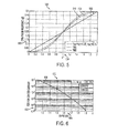
FIG. 5 illustrates agraph 500 of CPM phase response with time, in accordance with aspects of the present invention. - As illustrated in the figure, an y-
axis 502 represents the CPM phase response in radians and ax -axis 504 represents the time normalized by symbol duration or time multiplied by symbol rate (t/T). CPM phase response is represented by a function q(t).Graph 500 includes acurve 506 which represents the phase response for a rectangular CPM (qRE(t)) and acurve 508 which represents the phase response for a raised-cosine CPM (qRC(t)).Graph 500 also includes acurve 510 in accordance with an aspect of the present invention, which represents the average phase response (qAV(t)) calculated as:
graph 500. Values of α RE and α RC may be programmable in order to achieve a particular phase response. - Function q(t) shapes power spectrum density at the modulator. Each of
curves Curves CPM 110 as described with reference toFIG. 1 . -
Curve 506 illustrates the phase response of a CPM signal having with power spectrum having a narrow main lobe but very large spectrum side lobes.Curve 508 illustrates the phase response of a CPM signal yielding a power spectrum which has very small spectral side lobes but very large main lobe. The proposed phase response, in accordance with an aspect of the present invention, may be illustrated ascurve 510, which may be represented as a weighted average of the responses ofcurves Curve 510 illustrates the phase response of a CPM signal whose spectral main lobes and side lobes can be shaped to improve resilience to ACI.CPM 302 andCPM correlator bank 402 may operate, in accordance with an aspect of the present invention, in order to provide a phase response using function qav(t) resulting in an improved FER. -
CPM 302 andCPM correlator bank 402 may operate in accordance with proposed modulator code parameters as described below with reference to Table 1:Table 1 b/s/Hz Alphabet size M Modulation index h Pulse width Pulse shape AV FEC Code Rate Δ fT 0.5 4 2/5 2 α RE = 0.02
α RC =0.98(5,7)octal 1/2 2.0 0.75 4 1/3 2 α RE = 0.25
α RC =0.75(5, 7)octal 1/2 1.333 1.1 4 2/7 2 α RE = 0.25
α RC =0.75(5, 7)octal 2/3 1.21 1.25 4 2/7 2 α RE = 0.25
α RC =0.75(5, 7)octal 2/3 1.067 1.5 4 1/4 2 α RE = 0.25
α RC =0.75(15,17)octal 4/5 1.0667 1.8 4 1/5 2 α RE = 0.35
α RC =0.65(15,17)octal 6/7 0.974 - As illustrated in Table 1,
column 1 displays "b/s/Hz", which indicates transmission rate as bits/sec/Hertz. Typically, as the rate of transmission increases, the amount of energy required also increases. -
Column 2 displays "Alphabet size M," which indicates the maximum number of different symbols that may be transmitted. Consider for example a situation where the alphabet size is two, wherein a symbol may be transmitted on one of two positions on a circular circumference, e.g., the 12:00 position of a clock and the 6:00 position of a clock. In this example situation, suppose the transmitted symbol lies on the 12:00 position of a clock and the corresponding received symbol lies on the 2:00 position of a clock. In such a case, the receiver will likely be able to correctly determine that the transmitted symbol was on the 12:00 position of a clock. Clearly, when the alphabet size is two, the amount of data/symbol is limited to one of two, but the likelihood of determining the correctly transmitted symbol is relatively large. - Now consider the example situation where the alphabet size is 4, wherein a symbol may be transmitted on one of four positions on a circular circumference, e.g., the 12:00, the 3:00, the 6:00 and the 9:00 positions on a clock. In this example situation, suppose the transmitted symbol lies on the 12:00 position of a clock, but the received symbol lies on the 2:00 position of a clock. In such a case, the receiver may incorrectly determine that the transmitted symbol was located on the 3:00 position of a clock. Clearly, when the alphabet size is four, the amount of data/symbol is limited to one of four or twice that in the situation where the alphabet size is two, but the likelihood of determining the correctly transmitted symbol is much smaller than the situation where the alphabet size is two. Generally, as the alphabet size increases, the amount of data that can be transmitted per symbol increases and the probability of incorrectly determining a transmitted symbol also increases.
-
Column 3 displays "Modulation index h," wherein h is a parameter that shapes the power spectrum inCPM 302 andCPM correlator bank 402. Further, h also affects the frame error rate performance of CPM. In particular, in a single-carrier system (i.e. when there are no other carriers sharing the channel), a larger h is desirable because it results in an improved error rate performance. However, a larger h also results in the CPM signal having a wider power spectrum. Hence in the presence of adjacent carrier interference, there is a trade-off between the performance improvement from choosing a larger h and the performance degradation resulting from the increase in ACI caused by the wider power spectrum due to a large h. -
Column 4 displays "Pulse width in symbol duration". In particular, the pulse width in each of the entries of Table 1 is "2," indicating the pulse width is limited to a two-symbol duration, i.e., the duration it takes to transmit two symbols. -
Column 5 displays "Pulse Shape." The shape in each of the entries of Table 1 is AV, which corresponds to a linear combination of a raised-cosine pulse shape and a rectangular pulse shape, in accordance with an aspect of the present invention. -
Column 6 displays forward error correction or "FEC". The (5, 7)octal entries indicate a 4-state correction, whereas the (15, 17)octal entries indicate an 8 state correction. -
Column 7 displays "Code Rate", which indicates redundancy in the transmitted code. For example, a code rate of 1/2 implies for every information bit entering the convolutional code, the convolutional code generated two codebits. Similarly, a code rate of 2/3 implies that for every two information bits entering the convolutional code, the convolutional code generated 3 codebits. The higher the redundancy (i.e. lower the code rate), the higher the probability that the information bit with be received without error. However, the higher the redundancy, lower the achievable spectral efficiency. -
Column 7 displays "Δ f T", which indicates carrier spacing in frequency. As the carrier spacing decreases, more streams may be placed on a channel. However, as the carrier spacing decreases, ACI increases, thus increasing the probability of error for a received symbol. - Different rows in Table 1 indicate the potentially optimum combination of parameters listed in
column 2 throughcolumn 7 for a particular transmission and reception rate incolumn 1. The proposed CPM scheme using the parameters listed in Table 1 provide improved signal to noise ratio for a given frame error rate. For example, for transmitting and receiving at a rate of 1.1 b/s/Hz, and using: an alphabet size of 4 symbols; a modulation index h of 2/7; a pulse width of 2 and pulse shape based on a AV q function in accordance with an aspect of the present invention; an FEC of (5, 7)octal; a code rate of 2/3 and a carrier spacing of 1.21 may operate to minimize transmission error and concurrently minimize transmission power. Of course any of the parameters from columns 2-7 of Table 1, within the row corresponding to a transmission rate of 1.1 may be modified. However, such a change may operate to increase the transmission error and/or increase the required transmission power needed in order to maintain the desired transmission and reception rate. - Frame error rates for code and modulation parameters in accordance with an aspect of the present invention listed in Table 1 will now described further with respect to
FiGs. 6-11 . For the simulation analysis, it was assumed that all interfering carriers are 3dB stronger than the center carrier. For the simulation analysis, a maximum of 30 iterations were performed for operation with respect to theCPM detector 204 and binaryconvolutional decoder 208. - As shown in
row 1 of Table 1, for a 0.5b/s/Hz, alphabet size required is 4 symbols. Modulation index h is configured to 2/5. Pulse width spans 2 symbol duration and pulse shape based on an AV q function in accordance with an aspect of the present invention; FEC is (5, 7)octal is configured indicating a 4 state convolutional code. Code rate is configured for 1/2. Δ f T is configured for 2.0. -
FIG. 6 illustrates agraph 600 of FER with signal to noise ratio Eb/N0 for center carrier at 0.5 b/s/Hz, in accordance with aspects of the present invention. - As illustrated in the figure, an y-
axis 602 represents the FER for center carrier (logarithmic scale wherein the error rate does not have a unit) and ax -axis 604 represents the signal to noise ratio or energy/information bit Eb/N0 (logarithmic scale in dB).Graph 600 includes acurve 606. -
Graph 600 illustrates the FER performance using therate 1/2 binary convolutional code with generators (5,7)octal in AWGN for the center carrier at 0.5 b/s/Hz. The length of the information sequence is Nu = 1504 bits. The modulation parameters are configured as M=4, h=2/5 and 2AV. The multicarrier model assumes a total of four interfering carriers with +3dB ACI and Δ f T = 2.0. - As shown in
FIG. 6 ,curve 606 represents spectral efficiency for data rate of 0.5 b/s/Hz.Curve 606 indicates that signal to noise ratio increases with lower frame error rates. The FER performance versus signal to noise ratio Eb/N0 for higher data rates will be discussed further. - As shown in
row 2 of Table 1, for a 0.75 b/s/Hz rate, alphabet size required is 4 symbols. Modulation index h is configured to 1/3; a pulse width of 2 symbol duration and pulse shape based on a AV q function in accordance with an aspect of the present invention; FEC is (5, 7)octal is configured indicating a 4 state convolutional code. Code rate is configured for 1/2. Δ f T is configured for 1.333. -
FIG. 7 illustrates agraph 700 of FER with signal to noise ratio Eb/N0 for center carrier at 0.75 b/s/Hz, in accordance with aspects of the present invention. - As illustrated in the figure, an y-
axis 702 represents the FER for center carrier (logarithmic scale wherein the error rate does not have a unit) and ax -axis 704 represents the signal to noise ratio or energy/information bit Eb/N0 (logarithmic scale in dB).Graph 700 includes acurve 706. -
Graph 700 illustrates the FER performance using therate 1/2 binary convolutional code with generators (5,7)octal in AWGN for the center carrier at 0.75 b/s/Hz. The length of the information sequence is Nu = 1504 bits. The modulation parameters are configured as M=4, h=1/3 and 2AV. The multicarrier model assumes a total of four interfering carriers with +3dB ACI and Δ f T = 1.333. - As shown in
FIG. 7 ,curve 706 represents spectral efficiency for data rate of 0.75 b/s/Hz.Curve 706 indicates that signal to noise ratio increases with lower frame error rates. The FER performance versus signal to noise ratio Eb/N0 for higher data rates will be discussed further. - As shown in
row 3 of Table 1, for a 1.1 b/s/Hz rate, alphabet size required is 4 symbols. Modulation index h is configured to 2/7. A pulse width of 2 symbol duration and pulse shape based on a AV q function in accordance with an aspect of the present invention; FEC is (5, 7)octal is configured indicating a 4 state convolutional code. Code rate is configured for 2/3. Δ f T is configured for 1.21. FER performance versus Eb/N0 ofCPM 302 using the parameters ofrow 2 of Table 1 is shown inFIG. 7 . -
FIG. 8 illustrates agraph 800 of FER with signal to noise ratio Eb/N0 for center carrier at 1.1 b/s/Hz, in accordance with aspects of the present invention. - As illustrated in the figure, an y-
axis 802 represents the FER for center carrier (logarithmic scale) and ax -axis 804 represents the signal to noise ratio or energy/information bit Eb/N0 (logarithmic scale in dB).Graph 800 includes acurve 806. -
Graph 800 shows the FER performance using therate 2/3 binary convolutional code with generators (5,7)octal in AWGN for the center carrier at 1.1 b/s/Hz. The length of the information sequence is Nu = 1504 bits. The modulation parameters are M=4, h=2/7 and 2AV. The multicarrier model assumes a total of four interfering carriers with +3dB ACI and Δ f T = 1.21. - As shown in
FIG. 8 ,curve 806 represents spectral efficiency for data rate of 1.1 b/s/Hz.Curve 806 indicates that signal to noise ratio increases with lower frame error rates. The FER performance versus signal to noise ratio Eb/N0 for higher data rates will be discussed further. - As shown in
row 4 of Table 1, for a 1.25 b/s/Hz rate, alphabet size required is 4 symbols. Modulation index h is configured to 2/7. A pulse width of 2 symbol duration and pulse shape based on a AV q function in accordance with an aspect of the present invention. FEC is (5, 7)octal, is configured indicating a 4 state convolutional code. Code rate is configured for 2/3. Δ f T is configured for 1.067. FER performance versus Eb/N0 ofCPM 302 for these parameters is shown inFIG. 9 . -
FIG. 9 illustrates agraph 900 of FER with signal to noise ratio Eb/N0 for center carrier at 1.25 b/s/Hz, in accordance with aspects of the present invention. - As illustrated in the figure, an y-
axis 902 represents the FER for center carrier (logarithmic scale) and a x-axis 904 represents the signal to noise ratio or energy/information bit Eb/N0 (logarithmic scale in dB).Graph 900 includes acurve 906. -
Graph 900 shows the FER performance using therate 2/3 binary convolutional code with generators (5,7)octal in AWGN for the center carrier at 1.25 b/s/Hz. The length of the information sequence is Nu = 1504 bits. The modulation parameters are M=4, h=2/7, 2AV. The multicarrier model assumes a total of four interfering carriers with +3dB ACI and Δ f T = 1.067. - As shown in
FIG. 9 ,curve 906 represents spectral efficiency for data rate of 1.25 b/s/Hz.Curve 906 indicates that signal to noise ratio increases with lower frame error rates. The FER performance versus signal to noise ratio Eb/N0 for even higher data rate will be discussed further. - As shown in
row 5 of Table 1, for a 1.5 b/s/Hz rate, alphabet size required is 4 symbols. Modulation index h is configured to 1/4. A pulse width of 2 symbol duration and pulse shape based on an AV q function in accordance with an aspect of the present invention. FEC is (15, 17)octal, is configured indicating a 8 state convolutional code. Code rate is configured for 4/5. Δ f T is configured for 1.0667. FER performance versus Eb/N0 ofCPM 302 for these parameters is shownFIG. 10 . -
FIG. 10 illustrates agraph 1000 of FER with signal to noise ratio Eb/N0 for center carrier at 1.5 b/s/Hz, in accordance with aspects of the present invention. - As illustrated in the figure, an y-
axis 1002 represents the FER for center carrier (logarithmic scale) and ax -axis 1004 represents the signal to noise ratio or energy/information bit Eb/N0 (logarithmic scale in dB).Graph 1000 includes acurve 1006. -
Graph 1000 shows the FER performance using the 4/5 binary convolutional code with generators (15,17)octal in AWGN for the center carrier at 1.5 b/s/Hz. The length of the information sequence is Nu = 1504 bits. The modulation parameters are M=4, h=1/4, 2AV. The multicarrier model assumes a total of four interfering carriers with +3dB ACI and Δ f T =1.0667.Curve 1006 indicates that signal to noise ratio increases with lower frame error rates. -
FIG. 11 illustrates agraph 1100 of FER with signal to noise ratio Eb/N0 for center carrier at 1.8 b/s/Hz, in accordance with aspects of the present invention. - As illustrated in the figure, an y-
axis 1102 represents the FER for center carrier (logarithmic scale) and ax -axis 1104 represents the signal to noise ratio or energy/information bit Eb/N0 (logarithmic scale in dB).Graph 1100 includes acurve 1106. -
FiGs. 3-4 illustratetransmitter 300 andreceiver 400 using proposed CPM scheme, in accordance with aspects of the present invention. As illustrated inFIG. 5 , CPM phase response was calculated and was represented by function qAV . The proposed phase response qAV , which may be represented as a weighted average of the rectangular and raised-cosine responses, may operate to provide an optimum response for minimizing FER for a given data rate, for example, as shown in Table 1. A CPM scheme, in accordance with aspects of the present invention, using the parameters listed in Table 1 may operate to provide improved signal to noise ratio for a given frame error rate. Also, FER for center carrier was shown with respect to Eb/N0 using the CPM scheme, in accordance with aspects of the present invention, at example data rates of 0.5b/s/Hz 0.75b/s/Hz, 1.1b/s/Hz, 1.25b/s/Hz and 1.5b/s/Hz and 1.8 b/s/Hz. It should be noted that other data rates may be used in accordance with aspects of the present invention. A data rate, or spectral efficiency, may be chosen based,
- The foregoing description of various preferred embodiments of the invention have been presented for purposes of illustration and description. It is not intended to be exhaustive or to limit the invention to the precise forms disclosed, and obviously many modifications and variations are possible in light of the above teaching. The example embodiments, as described above, were chosen and described in order to best explain the principles of the invention and its practical application to thereby enable others skilled in the art to best utilize the invention in various embodiments and with various modifications as are suited to the particular use contemplated. It is intended that the scope of the invention be defined by the claims appended hereto.
A new coded continuous phase modulation (CPM) scheme is proposed to enhance physical layer performance of the current DVB-RCS standard for a satellite communication system. The proposed CPM scheme uses a phase pulse design and combination of modulation parameters to shape the power spectrum of CPM signal in order to improve resilience to adjacent channel interference (ACI). Additionally, it improves error rate performance at both high and low frame error rates using low complexity binary convolutional codes and S-random bit interleaving. Phase response using the proposed CPM scheme is a weighted average of the conventional rectangular and raised-cosine responses and provides optimum response to minimize frame error rate for a given data rate.
Claims (14)
- A device (300, 400) comprising:a) in a configuration to output a modulated signal (304, 124, 212):a bit-to-symbol generator (108) operable to output a symbol stream (120) of a plurality of different types of symbols, the symbol stream (120) being based on a source data stream (114); anda continuous phase modulator (302) operable to output a modulated signal (304, 124, 212) based on the symbol stream (114), orb) in a configuration for use with a modulated signal (304, 124, 212):a correlator (402) operable to output a demodulated stream based on the modulated signal (124, 212); anda detector (204) operable to output a symbol stream of a plurality of differenttypes of symbols based on the demodulated stream;
wherein the device is configured such that
the modulated signal (304) is based on an alphabet size of the plurality of different types of symbols, a modulation index h, a pulse shape and a pulse width,
wherein qav is a continuous phase modulation phase response of a pulse shape for the modulator as a function of time,
wherein qrc is a continuous phase modulation phase response of raised-cosine-shaped pulses as a function of time,
wherein qre is a continuous phase modulation phase response of rectangular-shaped pulses as a function of time, and
wherein qav is a linear function of qrc and qre . - The device (300, 400) of claim 1, wherein, in case a), the continuous phase modulator (302) or, in case b), the correlator (402) has a (5, 7)octal forward error correction.
- The device (300, 400) of claim 2, wherein, in case a), the continuous phase modulator (302) or, in case b), the correlator (402) has a 2/7 modulation index h and a 2/3 redundancy code rate.
- The device (300, 400) of claim 3, wherein, in case a), the continuous phase modulator (302) or, in case b), the correlator (402)
has a 1.1 b/s/Hz transmission rate and a 1.21 Δ f T carrier spacing, or
has a 1.25 b/s/Hz transmission rate and a 1.067 Δ f T carrier spacing. - The device (300, 400) of claim 2, wherein, in case a), the continuous phase modulator (302) or, in case b), the correlator (402)
has a 2/5 modulation index h, a 1/2 redundancy code rate, a 0.5 b/s/Hz transmission rate, and a 2.0 Δ f T carrier spacing; or
has a 1/3 modulation index h, a 1/2 redundancy code rate, a 0.75 b/s/Hz transmission rate, and a 1.333 Δ f T carrier spacing. - The device (300, 400) of claim 1, wherein, in case a), the continuous phase modulator (302) or, in case b), the correlator (402) has a (15, 17)octal forward error correction.
- The device (300, 400) of claim 6, wherein, in case a), the continuous phase modulator (302) or, in case b), the correlator (402)
has a 1/4 modulation index h, a 4/5 redundancy code rate, a 1.5 b/s/Hz transmission rate, and a 1.0667 Δ f T carrier spacing, or
has a 1/5 modulation index h, a 6/7 redundancy code rate, a 1.8 b/s/Hz transmission rate, and a 0.974 Δ f T carrier spacing. - A method comprising:eithera) outputting, by way of a bit-to-symbol generator (108), a symbol stream of a plurality of different types of symbols, the symbol stream being based on a source data stream (114); and
outputting, by way of a continuous phase modulator (302), a modulated signal based on the symbol stream,orb)wherein the method further is characterized in that
receiving a modulated signal;
outputting, by way of a correlator, a demodulated stream based on the modulated stream signal; and
outputting, by way of a detector, a symbol stream of a plurality of different types of symbols, the symbol stream being based on the demodulated stream,the modulated signal is based on an alphabet size of the plurality of different types of symbols, a modulation index h, a pulse shape and a pulse width,
wherein qav is a continuous phase modulation phase response of modulated pulses shape as a function of time,
wherein qrc is a continuous phase modulation phase response of raised-cosine-shaped pulses as a function of time,
wherein qre is a continuous phase modulation phase response of rectangular-shaped pulses as a function of time, and
wherein qav is a linear function of qrc and qre . - The method of claim 8, wherein, in case a), the continuous phase modulator (302) or, in case b), the correlator (402) has a (5, 7)octal forward error correction.
- The method of claim 9, wherein, in case a), the continuous phase modulator (302) or, in case b), the correlator (402) has a 2/7 modulation index h and a 2/3 redundancy code rate.
- The method of claim 10, wherein, in case a), the continuous phase modulator (302) or, in case b), the correlator (402)
has a 1.1 b/s/Hz transmission rate and a 1.21 Δ f T carrier spacing, or
has a 1.25 b/s/Hz transmission rate and a 1.067 Δ f T carrier spacing. - The method of claim 9, wherein, in case a), the continuous phase modulator (302) or, in case b), the correlator (402)
has a 2/5 modulation index h, a 1/2 redundancy code rate, a 0.5 b/s/Hz transmission rate, and a 2.0 Δ f T carrier spacing, or
has a 1/3 modulation index h, a 1/2 redundancy code rate, a 0.75 b/s/Hz transmission rate, and a 1.333 Δ f T carrier spacing. - The method of claim 9, wherein, in case a), the continuous phase modulator (302) or, in case b), the correlator (402) has a (15, 17)octal forward error correction.
- The method of claim 13, wherein, in case a), the continuous phase modulator (302) or, in case b), the correlator (402)
has a 1/4 modulation index h, a 4/5 redundancy code rate, a 1.5 b/s/Hz transmission rate, and a 1.0667 Δ f T carrier spacing, or
has a 1/5 modulation index h, a 6/7 redundancy code rate, a 1.8 b/s/Hz transmission rate, and a 0.974 Δ f T carrier spacing.
Applications Claiming Priority (2)
| Application Number | Priority Date | Filing Date | Title |
|---|---|---|---|
| US33107810P | 2010-05-04 | 2010-05-04 | |
| US12/894,358 US8903012B2 (en) | 2010-05-04 | 2010-09-30 | Continuous phase modulation for satellite communications |
Publications (3)
| Publication Number | Publication Date |
|---|---|
| EP2385662A2 true EP2385662A2 (en) | 2011-11-09 |
| EP2385662A3 EP2385662A3 (en) | 2014-04-02 |
| EP2385662B1 EP2385662B1 (en) | 2017-09-06 |
Family
ID=44484947
Family Applications (1)
| Application Number | Title | Priority Date | Filing Date |
|---|---|---|---|
| EP11164857.2A Active EP2385662B1 (en) | 2010-05-04 | 2011-05-04 | Improved continuous phase modulation for satellite communications |
Country Status (2)
| Country | Link |
|---|---|
| US (1) | US8903012B2 (en) |
| EP (1) | EP2385662B1 (en) |
Cited By (1)
| Publication number | Priority date | Publication date | Assignee | Title |
|---|---|---|---|---|
| CN106160927A (en) * | 2015-04-09 | 2016-11-23 | 扬智科技股份有限公司 | Decoding method and device |
Families Citing this family (5)
| Publication number | Priority date | Publication date | Assignee | Title |
|---|---|---|---|---|
| US8982933B2 (en) * | 2011-06-27 | 2015-03-17 | Harris Corporation | Communications system including jammer using continuous phase modulation (CPM) and associated methods |
| CN104079517A (en) * | 2014-06-19 | 2014-10-01 | 哈尔滨工程大学 | Continuous phase modulation achieving method based on pulse function weighing |
| US9894687B2 (en) * | 2015-11-20 | 2018-02-13 | Hughes Network Systems, Llc | Methods and apparatuses for providing random access communication |
| CN112202699B (en) * | 2016-01-11 | 2022-01-21 | 中兴通讯股份有限公司 | Data modulation and demodulation method, frame generation method and node of multi-carrier system |
| CN112153703A (en) | 2016-08-15 | 2020-12-29 | 华为技术有限公司 | Method and apparatus for transmitting wake-up packet in communication system |
Family Cites Families (8)
| Publication number | Priority date | Publication date | Assignee | Title |
|---|---|---|---|---|
| US5834986A (en) | 1997-10-06 | 1998-11-10 | Trw Inc. | Direct 2nd derivative synthesis method for controlling sidelobe energy in an MSK modulated signal |
| US7430257B1 (en) * | 1998-02-12 | 2008-09-30 | Lot 41 Acquisition Foundation, Llc | Multicarrier sub-layer for direct sequence channel and multiple-access coding |
| US7418043B2 (en) * | 2000-07-19 | 2008-08-26 | Lot 41 Acquisition Foundation, Llc | Software adaptable high performance multicarrier transmission protocol |
| US6968021B1 (en) | 2001-09-24 | 2005-11-22 | Rockwell Collins | Synchronization method and apparatus for modems based on jointly iterative turbo demodulation and decoding |
| US7205859B2 (en) | 2003-03-17 | 2007-04-17 | Harris Corporation | Method and apparatus for sub sample-per-symbol demodulator for a spectrally efficient waveform with an LPI feature |
| US7630356B2 (en) * | 2004-04-05 | 2009-12-08 | Nortel Networks Limited | Methods for supporting MIMO transmission in OFDM applications |
| US8160166B2 (en) * | 2008-10-01 | 2012-04-17 | Harris Corporation | Orthogonal frequency division multiplexing (OFDM) communications device and method that incorporates low PAPR preamble with circuit for measuring frequency response of the communications channel |
| WO2011057252A1 (en) * | 2009-11-09 | 2011-05-12 | Sonosite, Inc. | Systems and methods for beam enhancement |
-
2010
- 2010-09-30 US US12/894,358 patent/US8903012B2/en active Active
-
2011
- 2011-05-04 EP EP11164857.2A patent/EP2385662B1/en active Active
Cited By (1)
| Publication number | Priority date | Publication date | Assignee | Title |
|---|---|---|---|---|
| CN106160927A (en) * | 2015-04-09 | 2016-11-23 | 扬智科技股份有限公司 | Decoding method and device |
Also Published As
| Publication number | Publication date |
|---|---|
| EP2385662A3 (en) | 2014-04-02 |
| EP2385662B1 (en) | 2017-09-06 |
| US8903012B2 (en) | 2014-12-02 |
| US20110274216A1 (en) | 2011-11-10 |
Similar Documents
| Publication | Publication Date | Title |
|---|---|---|
| EP2421213B1 (en) | Phase pulse system and method for bandwidth and energy efficient continuous phase modulation | |
| JP6096922B2 (en) | Check and irregular non-systematic IRA code encoding and decoding system and method | |
| EP0663775B1 (en) | Method and apparatus for communicating multilevel modulated data using concatenated coding | |
| CN102075487B (en) | Multidimensional constellation mapping based coding and modulating method, demodulating and decoding method and system | |
| US10128983B2 (en) | Transmitter and receiver devices performing repetition before interleaving and puncturing after interleaving and methods thereof | |
| EP2385662B1 (en) | Improved continuous phase modulation for satellite communications | |
| KR20160086394A (en) | Transmission and receiving method in a wireless communication system | |
| EP2615759A2 (en) | Method and apparatus for transmitting/receiving data using satellite channel | |
| US7620881B2 (en) | System and method for communicating data using iterative equalizing and decoding and recursive inner code | |
| CN103532663A (en) | Frequency hopping fountain code system and transmission method thereof | |
| US6944206B1 (en) | Rate one coding and decoding methods and systems | |
| Chang et al. | Iterative channel decoding of FEC-based multiple-description codes | |
| Phoel et al. | Frequency-hop spread spectrum with quadrature amplitude modulation and error-control coding | |
| Remlein | Energy efficient continuous phase modulation signals for satellite intelligent transportation systems | |
| Chen et al. | Network‐turbo‐coding‐based cooperation with distributed space‐time block codes | |
| KR101483228B1 (en) | Apparatus and method for encoding and decoding | |
| Popovic et al. | Bit-interleaved low density spread (BI-LDS) transmission | |
| EP2592772A1 (en) | Improved time diversity for rotated constellations | |
| Stopler et al. | Capacity and error probability in single-tone and multitone multiple access over an impulsive channel | |
| Kuswidiastuti et al. | Implementation and performance analysis of convolution codeon WARP (wireless open access research platform) | |
| Qazi et al. | Performance Evaluation of Error Correcting Techniques for OFDM Systems | |
| Khalili | Design and Simulation of Coded-Modulation Using Turbo Trellis Coding and Multi-Layer Modulations | |
| Yar et al. | Performance of Reed-Solomon coded M-ary modulation systems with overlapped symbols | |
| Ajibodu et al. | Reduction of white noise in a communication channel | |
| Akhter | Performance of channel interleaved turbo coded system for high rate mobile satellite communications |
Legal Events
| Date | Code | Title | Description |
|---|---|---|---|
| AK | Designated contracting states |
Kind code of ref document: A2 Designated state(s): AL AT BE BG CH CY CZ DE DK EE ES FI FR GB GR HR HU IE IS IT LI LT LU LV MC MK MT NL NO PL PT RO RS SE SI SK SM TR |
|
| AX | Request for extension of the european patent |
Extension state: BA ME |
|
| PUAI | Public reference made under article 153(3) epc to a published international application that has entered the european phase |
Free format text: ORIGINAL CODE: 0009012 |
|
| PUAL | Search report despatched |
Free format text: ORIGINAL CODE: 0009013 |
|
| AK | Designated contracting states |
Kind code of ref document: A3 Designated state(s): AL AT BE BG CH CY CZ DE DK EE ES FI FR GB GR HR HU IE IS IT LI LT LU LV MC MK MT NL NO PL PT RO RS SE SI SK SM TR |
|
| AX | Request for extension of the european patent |
Extension state: BA ME |
|
| RIC1 | Information provided on ipc code assigned before grant |
Ipc: H04L 1/00 20060101ALI20140221BHEP Ipc: H04L 25/03 20060101AFI20140221BHEP Ipc: H04L 27/20 20060101ALI20140221BHEP |
|
| 17P | Request for examination filed |
Effective date: 20140804 |
|
| RBV | Designated contracting states (corrected) |
Designated state(s): AL AT BE BG CH CY CZ DE DK EE ES FI FR GB GR HR HU IE IS IT LI LT LU LV MC MK MT NL NO PL PT RO RS SE SI SK SM TR |
|
| REG | Reference to a national code |
Ref country code: DE Ref legal event code: R079 Ref document number: 602011041230 Country of ref document: DE Free format text: PREVIOUS MAIN CLASS: H04L0027200000 Ipc: H04L0025030000 |
|
| GRAP | Despatch of communication of intention to grant a patent |
Free format text: ORIGINAL CODE: EPIDOSNIGR1 |
|
| STAA | Information on the status of an ep patent application or granted ep patent |
Free format text: STATUS: GRANT OF PATENT IS INTENDED |
|
| RIC1 | Information provided on ipc code assigned before grant |
Ipc: H04L 1/00 20060101ALI20170328BHEP Ipc: H04L 25/03 20060101AFI20170328BHEP Ipc: H04L 27/20 20060101ALI20170328BHEP |
|
| INTG | Intention to grant announced |
Effective date: 20170418 |
|
| GRAS | Grant fee paid |
Free format text: ORIGINAL CODE: EPIDOSNIGR3 |
|
| GRAA | (expected) grant |
Free format text: ORIGINAL CODE: 0009210 |
|
| STAA | Information on the status of an ep patent application or granted ep patent |
Free format text: STATUS: THE PATENT HAS BEEN GRANTED |
|
| AK | Designated contracting states |
Kind code of ref document: B1 Designated state(s): AL AT BE BG CH CY CZ DE DK EE ES FI FR GB GR HR HU IE IS IT LI LT LU LV MC MK MT NL NO PL PT RO RS SE SI SK SM TR |
|
| REG | Reference to a national code |
Ref country code: GB Ref legal event code: FG4D |
|
| REG | Reference to a national code |
Ref country code: CH Ref legal event code: EP Ref country code: AT Ref legal event code: REF Ref document number: 927006 Country of ref document: AT Kind code of ref document: T Effective date: 20170915 |
|
| REG | Reference to a national code |
Ref country code: IE Ref legal event code: FG4D |
|
| REG | Reference to a national code |
Ref country code: DE Ref legal event code: R096 Ref document number: 602011041230 Country of ref document: DE |
|
| REG | Reference to a national code |
Ref country code: NL Ref legal event code: MP Effective date: 20170906 |
|
| REG | Reference to a national code |
Ref country code: LT Ref legal event code: MG4D |
|
| PG25 | Lapsed in a contracting state [announced via postgrant information from national office to epo] |
Ref country code: HR Free format text: LAPSE BECAUSE OF FAILURE TO SUBMIT A TRANSLATION OF THE DESCRIPTION OR TO PAY THE FEE WITHIN THE PRESCRIBED TIME-LIMIT Effective date: 20170906 Ref country code: NO Free format text: LAPSE BECAUSE OF FAILURE TO SUBMIT A TRANSLATION OF THE DESCRIPTION OR TO PAY THE FEE WITHIN THE PRESCRIBED TIME-LIMIT Effective date: 20171206 Ref country code: FI Free format text: LAPSE BECAUSE OF FAILURE TO SUBMIT A TRANSLATION OF THE DESCRIPTION OR TO PAY THE FEE WITHIN THE PRESCRIBED TIME-LIMIT Effective date: 20170906 Ref country code: SE Free format text: LAPSE BECAUSE OF FAILURE TO SUBMIT A TRANSLATION OF THE DESCRIPTION OR TO PAY THE FEE WITHIN THE PRESCRIBED TIME-LIMIT Effective date: 20170906 Ref country code: LT Free format text: LAPSE BECAUSE OF FAILURE TO SUBMIT A TRANSLATION OF THE DESCRIPTION OR TO PAY THE FEE WITHIN THE PRESCRIBED TIME-LIMIT Effective date: 20170906 |
|
| REG | Reference to a national code |
Ref country code: AT Ref legal event code: MK05 Ref document number: 927006 Country of ref document: AT Kind code of ref document: T Effective date: 20170906 |
|
| PG25 | Lapsed in a contracting state [announced via postgrant information from national office to epo] |
Ref country code: LV Free format text: LAPSE BECAUSE OF FAILURE TO SUBMIT A TRANSLATION OF THE DESCRIPTION OR TO PAY THE FEE WITHIN THE PRESCRIBED TIME-LIMIT Effective date: 20170906 Ref country code: RS Free format text: LAPSE BECAUSE OF FAILURE TO SUBMIT A TRANSLATION OF THE DESCRIPTION OR TO PAY THE FEE WITHIN THE PRESCRIBED TIME-LIMIT Effective date: 20170906 Ref country code: GR Free format text: LAPSE BECAUSE OF FAILURE TO SUBMIT A TRANSLATION OF THE DESCRIPTION OR TO PAY THE FEE WITHIN THE PRESCRIBED TIME-LIMIT Effective date: 20171207 Ref country code: BG Free format text: LAPSE BECAUSE OF FAILURE TO SUBMIT A TRANSLATION OF THE DESCRIPTION OR TO PAY THE FEE WITHIN THE PRESCRIBED TIME-LIMIT Effective date: 20171206 Ref country code: ES Free format text: LAPSE BECAUSE OF FAILURE TO SUBMIT A TRANSLATION OF THE DESCRIPTION OR TO PAY THE FEE WITHIN THE PRESCRIBED TIME-LIMIT Effective date: 20170906 |
|
| REG | Reference to a national code |
Ref country code: FR Ref legal event code: PLFP Year of fee payment: 8 |
|
| PG25 | Lapsed in a contracting state [announced via postgrant information from national office to epo] |
Ref country code: NL Free format text: LAPSE BECAUSE OF FAILURE TO SUBMIT A TRANSLATION OF THE DESCRIPTION OR TO PAY THE FEE WITHIN THE PRESCRIBED TIME-LIMIT Effective date: 20170906 |
|
| PG25 | Lapsed in a contracting state [announced via postgrant information from national office to epo] |
Ref country code: PL Free format text: LAPSE BECAUSE OF FAILURE TO SUBMIT A TRANSLATION OF THE DESCRIPTION OR TO PAY THE FEE WITHIN THE PRESCRIBED TIME-LIMIT Effective date: 20170906 Ref country code: CZ Free format text: LAPSE BECAUSE OF FAILURE TO SUBMIT A TRANSLATION OF THE DESCRIPTION OR TO PAY THE FEE WITHIN THE PRESCRIBED TIME-LIMIT Effective date: 20170906 Ref country code: RO Free format text: LAPSE BECAUSE OF FAILURE TO SUBMIT A TRANSLATION OF THE DESCRIPTION OR TO PAY THE FEE WITHIN THE PRESCRIBED TIME-LIMIT Effective date: 20170906 |
|
| PG25 | Lapsed in a contracting state [announced via postgrant information from national office to epo] |
Ref country code: IT Free format text: LAPSE BECAUSE OF FAILURE TO SUBMIT A TRANSLATION OF THE DESCRIPTION OR TO PAY THE FEE WITHIN THE PRESCRIBED TIME-LIMIT Effective date: 20170906 Ref country code: AT Free format text: LAPSE BECAUSE OF FAILURE TO SUBMIT A TRANSLATION OF THE DESCRIPTION OR TO PAY THE FEE WITHIN THE PRESCRIBED TIME-LIMIT Effective date: 20170906 Ref country code: SM Free format text: LAPSE BECAUSE OF FAILURE TO SUBMIT A TRANSLATION OF THE DESCRIPTION OR TO PAY THE FEE WITHIN THE PRESCRIBED TIME-LIMIT Effective date: 20170906 Ref country code: SK Free format text: LAPSE BECAUSE OF FAILURE TO SUBMIT A TRANSLATION OF THE DESCRIPTION OR TO PAY THE FEE WITHIN THE PRESCRIBED TIME-LIMIT Effective date: 20170906 Ref country code: EE Free format text: LAPSE BECAUSE OF FAILURE TO SUBMIT A TRANSLATION OF THE DESCRIPTION OR TO PAY THE FEE WITHIN THE PRESCRIBED TIME-LIMIT Effective date: 20170906 Ref country code: IS Free format text: LAPSE BECAUSE OF FAILURE TO SUBMIT A TRANSLATION OF THE DESCRIPTION OR TO PAY THE FEE WITHIN THE PRESCRIBED TIME-LIMIT Effective date: 20180106 |
|
| REG | Reference to a national code |
Ref country code: DE Ref legal event code: R097 Ref document number: 602011041230 Country of ref document: DE |
|
| PLBE | No opposition filed within time limit |
Free format text: ORIGINAL CODE: 0009261 |
|
| STAA | Information on the status of an ep patent application or granted ep patent |
Free format text: STATUS: NO OPPOSITION FILED WITHIN TIME LIMIT |
|
| PG25 | Lapsed in a contracting state [announced via postgrant information from national office to epo] |
Ref country code: DK Free format text: LAPSE BECAUSE OF FAILURE TO SUBMIT A TRANSLATION OF THE DESCRIPTION OR TO PAY THE FEE WITHIN THE PRESCRIBED TIME-LIMIT Effective date: 20170906 |
|
| 26N | No opposition filed |
Effective date: 20180607 |
|
| PG25 | Lapsed in a contracting state [announced via postgrant information from national office to epo] |
Ref country code: SI Free format text: LAPSE BECAUSE OF FAILURE TO SUBMIT A TRANSLATION OF THE DESCRIPTION OR TO PAY THE FEE WITHIN THE PRESCRIBED TIME-LIMIT Effective date: 20170906 |
|
| REG | Reference to a national code |
Ref country code: CH Ref legal event code: PL |
|
| PG25 | Lapsed in a contracting state [announced via postgrant information from national office to epo] |
Ref country code: MC Free format text: LAPSE BECAUSE OF FAILURE TO SUBMIT A TRANSLATION OF THE DESCRIPTION OR TO PAY THE FEE WITHIN THE PRESCRIBED TIME-LIMIT Effective date: 20170906 |
|
| REG | Reference to a national code |
Ref country code: IE Ref legal event code: MM4A |
|
| PG25 | Lapsed in a contracting state [announced via postgrant information from national office to epo] |
Ref country code: LI Free format text: LAPSE BECAUSE OF NON-PAYMENT OF DUE FEES Effective date: 20180531 Ref country code: CH Free format text: LAPSE BECAUSE OF NON-PAYMENT OF DUE FEES Effective date: 20180531 |
|
| PG25 | Lapsed in a contracting state [announced via postgrant information from national office to epo] |
Ref country code: IE Free format text: LAPSE BECAUSE OF NON-PAYMENT OF DUE FEES Effective date: 20180504 |
|
| PG25 | Lapsed in a contracting state [announced via postgrant information from national office to epo] |
Ref country code: MT Free format text: LAPSE BECAUSE OF NON-PAYMENT OF DUE FEES Effective date: 20180504 |
|
| PG25 | Lapsed in a contracting state [announced via postgrant information from national office to epo] |
Ref country code: TR Free format text: LAPSE BECAUSE OF FAILURE TO SUBMIT A TRANSLATION OF THE DESCRIPTION OR TO PAY THE FEE WITHIN THE PRESCRIBED TIME-LIMIT Effective date: 20170906 |
|
| PG25 | Lapsed in a contracting state [announced via postgrant information from national office to epo] |
Ref country code: HU Free format text: LAPSE BECAUSE OF FAILURE TO SUBMIT A TRANSLATION OF THE DESCRIPTION OR TO PAY THE FEE WITHIN THE PRESCRIBED TIME-LIMIT; INVALID AB INITIO Effective date: 20110504 Ref country code: PT Free format text: LAPSE BECAUSE OF FAILURE TO SUBMIT A TRANSLATION OF THE DESCRIPTION OR TO PAY THE FEE WITHIN THE PRESCRIBED TIME-LIMIT Effective date: 20170906 |
|
| PG25 | Lapsed in a contracting state [announced via postgrant information from national office to epo] |
Ref country code: MK Free format text: LAPSE BECAUSE OF NON-PAYMENT OF DUE FEES Effective date: 20170906 Ref country code: CY Free format text: LAPSE BECAUSE OF FAILURE TO SUBMIT A TRANSLATION OF THE DESCRIPTION OR TO PAY THE FEE WITHIN THE PRESCRIBED TIME-LIMIT Effective date: 20170906 |
|
| PG25 | Lapsed in a contracting state [announced via postgrant information from national office to epo] |
Ref country code: AL Free format text: LAPSE BECAUSE OF FAILURE TO SUBMIT A TRANSLATION OF THE DESCRIPTION OR TO PAY THE FEE WITHIN THE PRESCRIBED TIME-LIMIT Effective date: 20170906 |
|
| PGFP | Annual fee paid to national office [announced via postgrant information from national office to epo] |
Ref country code: LU Payment date: 20250429 Year of fee payment: 15 |
|
| PGFP | Annual fee paid to national office [announced via postgrant information from national office to epo] |
Ref country code: DE Payment date: 20250311 Year of fee payment: 15 |
|
| PGFP | Annual fee paid to national office [announced via postgrant information from national office to epo] |
Ref country code: BE Payment date: 20250410 Year of fee payment: 15 |
|
| PGFP | Annual fee paid to national office [announced via postgrant information from national office to epo] |
Ref country code: GB Payment date: 20260310 Year of fee payment: 16 |
|
| PGFP | Annual fee paid to national office [announced via postgrant information from national office to epo] |
Ref country code: FR Payment date: 20260309 Year of fee payment: 16 |