EP2385514A1 - Backlight unit and display device - Google Patents
Backlight unit and display device Download PDFInfo
- Publication number
- EP2385514A1 EP2385514A1 EP11160672A EP11160672A EP2385514A1 EP 2385514 A1 EP2385514 A1 EP 2385514A1 EP 11160672 A EP11160672 A EP 11160672A EP 11160672 A EP11160672 A EP 11160672A EP 2385514 A1 EP2385514 A1 EP 2385514A1
- Authority
- EP
- European Patent Office
- Prior art keywords
- light emitting
- emitting device
- light
- device assembly
- intensity
- Prior art date
- Legal status (The legal status is an assumption and is not a legal conclusion. Google has not performed a legal analysis and makes no representation as to the accuracy of the status listed.)
- Ceased
Links
Images



Classifications
-
- G—PHYSICS
- G09—EDUCATION; CRYPTOGRAPHY; DISPLAY; ADVERTISING; SEALS
- G09G—ARRANGEMENTS OR CIRCUITS FOR CONTROL OF INDICATING DEVICES USING STATIC MEANS TO PRESENT VARIABLE INFORMATION
- G09G3/00—Control arrangements or circuits, of interest only in connection with visual indicators other than cathode-ray tubes
- G09G3/20—Control arrangements or circuits, of interest only in connection with visual indicators other than cathode-ray tubes for presentation of an assembly of a number of characters, e.g. a page, by composing the assembly by combination of individual elements arranged in a matrix no fixed position being assigned to or needed to be assigned to the individual characters or partial characters
- G09G3/34—Control arrangements or circuits, of interest only in connection with visual indicators other than cathode-ray tubes for presentation of an assembly of a number of characters, e.g. a page, by composing the assembly by combination of individual elements arranged in a matrix no fixed position being assigned to or needed to be assigned to the individual characters or partial characters by control of light from an independent source
- G09G3/3406—Control of illumination source
-
- G—PHYSICS
- G02—OPTICS
- G02B—OPTICAL ELEMENTS, SYSTEMS OR APPARATUS
- G02B6/00—Light guides; Structural details of arrangements comprising light guides and other optical elements, e.g. couplings
- G02B6/0001—Light guides; Structural details of arrangements comprising light guides and other optical elements, e.g. couplings specially adapted for lighting devices or systems
- G02B6/0011—Light guides; Structural details of arrangements comprising light guides and other optical elements, e.g. couplings specially adapted for lighting devices or systems the light guides being planar or of plate-like form
- G02B6/0075—Arrangements of multiple light guides
- G02B6/0078—Side-by-side arrangements, e.g. for large area displays
- G02B6/008—Side-by-side arrangements, e.g. for large area displays of the partially overlapping type
-
- G—PHYSICS
- G02—OPTICS
- G02B—OPTICAL ELEMENTS, SYSTEMS OR APPARATUS
- G02B6/00—Light guides; Structural details of arrangements comprising light guides and other optical elements, e.g. couplings
- G02B6/0001—Light guides; Structural details of arrangements comprising light guides and other optical elements, e.g. couplings specially adapted for lighting devices or systems
- G02B6/0011—Light guides; Structural details of arrangements comprising light guides and other optical elements, e.g. couplings specially adapted for lighting devices or systems the light guides being planar or of plate-like form
- G02B6/0013—Means for improving the coupling-in of light from the light source into the light guide
- G02B6/0023—Means for improving the coupling-in of light from the light source into the light guide provided by one optical element, or plurality thereof, placed between the light guide and the light source, or around the light source
- G02B6/0031—Reflecting element, sheet or layer
-
- G—PHYSICS
- G02—OPTICS
- G02B—OPTICAL ELEMENTS, SYSTEMS OR APPARATUS
- G02B6/00—Light guides; Structural details of arrangements comprising light guides and other optical elements, e.g. couplings
- G02B6/0001—Light guides; Structural details of arrangements comprising light guides and other optical elements, e.g. couplings specially adapted for lighting devices or systems
- G02B6/0011—Light guides; Structural details of arrangements comprising light guides and other optical elements, e.g. couplings specially adapted for lighting devices or systems the light guides being planar or of plate-like form
- G02B6/0033—Means for improving the coupling-out of light from the light guide
- G02B6/005—Means for improving the coupling-out of light from the light guide provided by one optical element, or plurality thereof, placed on the light output side of the light guide
- G02B6/0055—Reflecting element, sheet or layer
-
- G—PHYSICS
- G02—OPTICS
- G02B—OPTICAL ELEMENTS, SYSTEMS OR APPARATUS
- G02B6/00—Light guides; Structural details of arrangements comprising light guides and other optical elements, e.g. couplings
- G02B6/0001—Light guides; Structural details of arrangements comprising light guides and other optical elements, e.g. couplings specially adapted for lighting devices or systems
- G02B6/0011—Light guides; Structural details of arrangements comprising light guides and other optical elements, e.g. couplings specially adapted for lighting devices or systems the light guides being planar or of plate-like form
- G02B6/0081—Mechanical or electrical aspects of the light guide and light source in the lighting device peculiar to the adaptation to planar light guides, e.g. concerning packaging
- G02B6/0083—Details of electrical connections of light sources to drivers, circuit boards, or the like
-
- G—PHYSICS
- G02—OPTICS
- G02B—OPTICAL ELEMENTS, SYSTEMS OR APPARATUS
- G02B6/00—Light guides; Structural details of arrangements comprising light guides and other optical elements, e.g. couplings
- G02B6/0001—Light guides; Structural details of arrangements comprising light guides and other optical elements, e.g. couplings specially adapted for lighting devices or systems
- G02B6/0011—Light guides; Structural details of arrangements comprising light guides and other optical elements, e.g. couplings specially adapted for lighting devices or systems the light guides being planar or of plate-like form
- G02B6/0081—Mechanical or electrical aspects of the light guide and light source in the lighting device peculiar to the adaptation to planar light guides, e.g. concerning packaging
- G02B6/0086—Positioning aspects
- G02B6/0088—Positioning aspects of the light guide or other optical sheets in the package
-
- G—PHYSICS
- G02—OPTICS
- G02B—OPTICAL ELEMENTS, SYSTEMS OR APPARATUS
- G02B6/00—Light guides; Structural details of arrangements comprising light guides and other optical elements, e.g. couplings
- G02B6/0001—Light guides; Structural details of arrangements comprising light guides and other optical elements, e.g. couplings specially adapted for lighting devices or systems
- G02B6/0011—Light guides; Structural details of arrangements comprising light guides and other optical elements, e.g. couplings specially adapted for lighting devices or systems the light guides being planar or of plate-like form
- G02B6/0081—Mechanical or electrical aspects of the light guide and light source in the lighting device peculiar to the adaptation to planar light guides, e.g. concerning packaging
- G02B6/0086—Positioning aspects
- G02B6/0091—Positioning aspects of the light source relative to the light guide
-
- G—PHYSICS
- G02—OPTICS
- G02F—OPTICAL DEVICES OR ARRANGEMENTS FOR THE CONTROL OF LIGHT BY MODIFICATION OF THE OPTICAL PROPERTIES OF THE MEDIA OF THE ELEMENTS INVOLVED THEREIN; NON-LINEAR OPTICS; FREQUENCY-CHANGING OF LIGHT; OPTICAL LOGIC ELEMENTS; OPTICAL ANALOGUE/DIGITAL CONVERTERS
- G02F1/00—Devices or arrangements for the control of the intensity, colour, phase, polarisation or direction of light arriving from an independent light source, e.g. switching, gating or modulating; Non-linear optics
- G02F1/01—Devices or arrangements for the control of the intensity, colour, phase, polarisation or direction of light arriving from an independent light source, e.g. switching, gating or modulating; Non-linear optics for the control of the intensity, phase, polarisation or colour
- G02F1/13—Devices or arrangements for the control of the intensity, colour, phase, polarisation or direction of light arriving from an independent light source, e.g. switching, gating or modulating; Non-linear optics for the control of the intensity, phase, polarisation or colour based on liquid crystals, e.g. single liquid crystal display cells
- G02F1/133—Constructional arrangements; Operation of liquid crystal cells; Circuit arrangements
- G02F1/1333—Constructional arrangements; Manufacturing methods
- G02F1/1335—Structural association of cells with optical devices, e.g. polarisers or reflectors
- G02F1/1336—Illuminating devices
- G02F1/133601—Illuminating devices for spatial active dimming
-
- G—PHYSICS
- G09—EDUCATION; CRYPTOGRAPHY; DISPLAY; ADVERTISING; SEALS
- G09G—ARRANGEMENTS OR CIRCUITS FOR CONTROL OF INDICATING DEVICES USING STATIC MEANS TO PRESENT VARIABLE INFORMATION
- G09G2310/00—Command of the display device
- G09G2310/02—Addressing, scanning or driving the display screen or processing steps related thereto
- G09G2310/0232—Special driving of display border areas
-
- G—PHYSICS
- G09—EDUCATION; CRYPTOGRAPHY; DISPLAY; ADVERTISING; SEALS
- G09G—ARRANGEMENTS OR CIRCUITS FOR CONTROL OF INDICATING DEVICES USING STATIC MEANS TO PRESENT VARIABLE INFORMATION
- G09G2320/00—Control of display operating conditions
- G09G2320/02—Improving the quality of display appearance
- G09G2320/0233—Improving the luminance or brightness uniformity across the screen
-
- G—PHYSICS
- G09—EDUCATION; CRYPTOGRAPHY; DISPLAY; ADVERTISING; SEALS
- G09G—ARRANGEMENTS OR CIRCUITS FOR CONTROL OF INDICATING DEVICES USING STATIC MEANS TO PRESENT VARIABLE INFORMATION
- G09G2320/00—Control of display operating conditions
- G09G2320/06—Adjustment of display parameters
- G09G2320/0626—Adjustment of display parameters for control of overall brightness
Definitions
- the present invention relates to a backlight unit, and more particularly to a backlight unit and a display device which can display uniform brightness throughout an entire screen.
- liquid crystal display device which is one of light receiving type flat display device used as computer monitors, or LCD-TV, and cellular phone terminals, has no spontaneous light emission capability, the liquid crystal display device has an external illumination light incident thereon selectively for producing a picture.
- the liquid crystal display device has the backlight unit mounted to a rear side of an inside thereof for emitting the light.
- the backlight unit there are a direct light type and an edge light type depending on an arrangement of a light emitting device.
- the direct light type is a type in which the light emitting device is mounted to a light guide plate provided to a rear side of a liquid crystal panel for directing the light to the rear side of the light guide plate
- the edge light type is a type in which the light emitting device is arranged on a side of the light guide plate for directing the light to the side of the light guide plate.
- a related art backlight unit has one or a plurality of light emitting device arrays covered with one light guide plate, the related art backlight unit is required to replace an entire light guide plate if the light guide plate has a defect at a portion thereof.
- the light guide plate has a scratch, stain, or deformation at a portion of a surface thereof, since brightness of the light at the portion of the screen of the display device matching to the surface is different from other portions distinctively, it has been required to replace the entire light guide plate for solving above problem.
- a size of the light guide plate can not but become larger in proportion to a size of the screen, requiring cumbersome and time consuming assembly work in fabrication of the backlight unit with such a large sized light guide plate.
- the present invention is directed to a backlight unit and a display device.
- An object of the present invention is to provide a backlight unit and a display device in which a backlight unit having a plurality of light emitting device assembly are provided for making assembly and management of the light emitting device assembly easy, and which can control intensity of a current applied to a light emitting device module for making brightness of a light on a screen is uniform throughout the screen.
- a backlight unit includes a bottom cover, a plurality of light emitting device assembly each having a light emitting device module including at least one light emitting device, the light emitting device assembly arranged on the bottom cover adjacent to one another, a power supply unit for supplying power to the light emitting device module in each of the light emitting device assembly, and a control unit for controlling the power supply unit such that, of the light emitting device modules of the light emitting device assembly, intensity of current supplied to a light emission device positioned at an edge region of each of the light emitting device assembly is different from the intensity of current supplied to the light emission device positioned at a middle region of each of the light emitting device assembly.
- control unit can control the intensity of the current applied to the light emission device positioned at the edge region of each of the light emitting device assembly to be greater than the intensity of the current applied to the light emission device positioned at the middle region of each of the light emitting device assembly.
- the light emitting device assembly can include a light guide plate arranged over the light emitting device module.
- the light guide plate can include a light incident portion for receiving the light from the light emitting device module, and a light forwarding portion for forwarding the light received thus through the light incident portion to a direction different from a direction of light incidence.
- the light emitting device module can be arranged on a lower side in a lateral direction thereof.
- control unit can control intensity of the current led to the light emitting device module such that quantities of the light incident on the light guide plate is the greatest at both ends of the light guide plate.
- the light emitting device module can include a plurality of light emitting devices and a circuit board having the light emitting devices arranged thereon, wherein a predetermined number of the light emitting devices can be grouped as a light emission unit such that a plurality of the light emission units form the light emitting device module, and the control unit leads the current to the light emission units independent from one another.
- control unit can control such that intensity of the current led to outermost light emission units positioned at both ends of the light emitting device module is greater than the intensity of the current led to the light emission units arranged between the outermost light emission units.
- control unit can control such that, of the light emission units in the light emitting device modules of the plurality of the light emitting device assembly mounted on the bottom cover, the intensity of the current led to the light emission units the most adjacent to edges of the bottom cover is the greatest of intensity of current led to all of the light emission units.
- the light emitting device assembly can be arranged in a matrix having a plurality of columns and a plurality of rows.
- control unit can control such that, of the light emission units in the light emitting device module of each of the plurality of light emitting device assembly, the intensity of the current led to the light emission units in the light emitting device modules of the light emitting device assembly arranged at the outermost sides is greatest.
- control unit can control such that, of the light emission units in the light emitting device module of each of the plurality of light emitting device assembly, the intensity of the current led to the light emission units in the light emitting device modules of the light emitting device assembly arranged at a lowest edge is greatest.
- a display device in another aspect of the present invention, includes a bottom cover, a plurality of light emitting device assembly each having a light emitting device module including at least one light emitting device, the light emitting device assembly arranged on the bottom cover adjacent to one another, an optical sheet for diffusing a light from the light emitting device assembly, a display panel provided in front of the optical sheet for producing an image, a power supply unit for supplying power to the light emitting device module in each of the light emitting device assembly, and a control unit for controlling the power supply unit such that, of the light emitting device modules of the light emitting device assembly, intensity of current supplied to a light emission device positioned at an edge region of each of the light emitting device assembly is different from the intensity of current supplied to the light emission device positioned at a middle region of each of the light emitting device assembly.
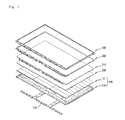
- FIG. 1 illustrates an exploded perspective view of a display device having a backlight unit in accordance with a preferred embodiment of the present invention.
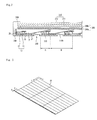
- FIG. 2 illustrates a longitudinal section of a display device in accordance with a preferred embodiment of the present invention.
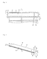
- FIG. 3 illustrates a perspective view showing a plurality of light emitting device assembly mounted to a backlight unit in accordance with a preferred embodiment of the present invention.
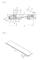
- FIG. 4 illustrates a plan view showing an arrangement of the plurality of light emitting device assembly in FIG. 3 .
- FIGS. 5 and 6 illustrate front perspective views of light emitting device assembly in accordance with a preferred embodiment of the present invention, respectively.
- FIG. 7 illustrates a rear perspective view of a light emitting device assembly in accordance with a preferred embodiment of the present invention.
- FIG. 8 illustrates a longitudinal section of a light emitting device assembly in accordance with a preferred embodiment of the present invention.
- FIG. 9 illustrates a perspective of a light guide plate in accordance with a preferred embodiment of the present invention.
- FIG. 10 illustrates a front perspective view of a light emitting device module in accordance with a preferred embodiment of the present invention.
- FIG. 11 illustrates a rear perspective view of a light emitting device module in accordance with a preferred embodiment of the present invention.
- FIG. 12 illustrates a front perspective view of a light emitting device module in accordance with a preferred embodiment of the present invention mounted to a reflective sheet.
- FIG. 13 illustrates a front view showing a matrix of light emitting device assembly arranged on a bottom cover in accordance with a preferred embodiment of the present invention.
- a layer (a film), a region, a pattern, or a structure is formed “on” or “under” a substrate
- a layer (a film) a region, a pad, or pattern the "on", or “under” implies that the layer (the film), the region, the pattern, or the structure is formed directly or indirectly.
- reference on the "on” or “under” is the drawing.
- a thickness or a size of a layer shown in a drawing is exaggerated, omitted or shown schematically for convenience or clarity of description. And, a size of an element is not shown to scale, perfectly.
- the display device of the embodiment includes a backlight unit 100, an optical sheet 200 in front of the backlight unit 100 for diffusing a light from the backlight unit 100, a display panel 210 in front of the optical sheet 200 for producing an image.
- fastening member 240 provided to edges of the backlight unit 100, the optical sheet 200, and the display panel 210 for holding and fastening the same together, and the fastening member 240 has a top cover 300 mounted thereto.
- the backlight unit 100 includes a bottom cover 110, and a plurality of light emitting device assembly 10 disposed adjacent to one another inside of the bottom cover.
- At least one beam member 250 arranged in a longitudinal or a transverse direction, for preventing the bottom cover 110 from deforming thermally or physically.
- the beam member 250 can be a lengthy extension in one direction, and can be formed of a metal having heat expansion coefficient smaller than the bottom cover 110 and stiffness greater than the bottom cover 110.
- a substrate for a power supply unit (not shown) which can supply power to the display panel 210 and other driving circuits.
- Each of the light emitting device assembly 10 includes a light emitting device module 13, a light guide plate 15 arranged adjacent to the light emitting device module 13, a reflective sheet 17 arranged in rear of the light guide plate 15, and a fastening cover 20 for fastening the light emitting device module 13, the light guide plate 15, and the reflective sheet 17 together.
- the light emitting device module 13 includes a light emitting device 11, and a circuit board 12 having the light emitting device arranged thereon.
- the light emitting device 11 is mounted to emit the light toward the light guide plate 15.
- a portion of the light emitting device assembly 10 having the light emitting device module 13 arranged thereon can be defined as a light emission region A, and a region thereof for receiving the light from the light emitting device module 13 and forwarding the light through the light guide plate 15 can be defined as a light forwarding region B.
- the light emitting device assembly 10 are arranged adjacent to one another along an inside surface of the bottom cover 110 such that a portion of the light guide plate 15 of one light emitting device assembly 10 can cover a portion of another light emitting device assembly 10 adjacent thereto.
- the bottom cover 110 has a heat dissipation projection 110b projected inward thereof for increasing heat dissipation efficiency by increasing a surface area of the bottom cover 110.
- the heat dissipation projection 110b is arranged between adjacent light emitting device assembly 10 for holding the light emitting device assembly 10.
- the heat dissipation projection 110b can be arranged in the space.
- the heat dissipation projection 110b can serve as a spacer which guides a mounting position of the light emitting device assembly 10, and, in a case the display device or the backlight unit is arranged upright, the heat dissipation projection 110b can serve as a supporting portion which supports a lower side of the light emitting device assembly 10.
- the optical sheet 200 over or on a front of the light guide plate 15 can have a diffusion sheet 200a, and/or a prism sheet 200b.
- the diffusion sheet 200a diffuses the light from the light guide plate 15 uniformly, and the light diffused by the diffusion sheet 200a can be converged onto the display panel 210 by the prism sheet 200b.
- the prism sheet 200b can have a horizontal or vertical prism sheet of one or more than one light intensity enhancing film, or the like.
- a guide pin (not shown) provided on the bottom cover 100 for holding the optical sheet 200.
- the optical sheet 200 can have a predetermined hole or recess for securing the optical sheet 200 to the bottom cover 100 as the guide pin (not shown) is coupled to the hole or recess.
- the display panel 210 is provided on or over the front of the optical sheet 200.
- the display panel 210 has a lower substrate 211 and an upper substrate 212 bonded together to face each other while maintaining a uniform cell gap, and a liquid crystal layer disposed between the two substrates 211 and 212.
- RGB color filters are provided not only on the upper substrate 212.
- the lower substrate 211 can include the color filters.
- a configuration of the display panel 210 of the upper substrate 211 and the lower substrate 212 is not limited to above, but the configuration can vary with liquid crystal layer driving systems.
- the display panel 210 can have a polarization film (not shown) arranged at least one of the upper surface (or a front surface) or a lower surface (rear surface) of the display panel 210.
- Edges of the display panel 210, the optical sheet 200, and the backlight unit 100 are surrounded and fastened by the fastening member 240, and the fastening member 240 is surrounded and fastened by the top cover 300.
- FIG. 3 there are a matrix of light emitting device assembly 10 arranged in x-, and y- axes. For an example, twenty seven light emitting device assembly 10 can be arranged in a 3X9 matrix.
- each of the light emitting device assembly 10 has the light emission region A for emission of the light and the light forwarding region B for forwarding the light, wherein the light emission region A of the light emitting device assembly 10 can be covered with the light forwarding region B of a lower side light emitting device assembly 10 except lowest light emitting device assembly 10.
- This structure prevents the light emission regions A of the light emitting device assembly 10 from exposing to an outside except the lowest light emitting device assembly 10.
- the light guide plates 15 of the light emitting device assembly 10 can be arranged spaced from one another in up/down, and left/right directions for certain extents, respectively.
- an x direction being the left/right direction
- a y direction being up/down direction
- a y direction being up/down direction
- an upper/lower region of a particular light emitting device assembly 10 is L1 and an upper/lower region of another light emitting device assembly 10 a portion of which overlaps with the upper/lower region L1 is L2.
- An edge 151 of the light guide plate 15 of the light emitting device assembly 10 having the L1 upper/lower region is spaced by a distance t2 from a stepped portion 152 of the light guide plate 15 of the light emitting device assembly 10 having the L2 upper/lower region.
- Distances like t1 and t2 are set thus to take thermal expansion of the light guide plate 15 of resin by heat from the light emitting device module 13 into account.
- the distances enable to prevent a particular light guide plate from being brought into contact with an adjacent light guide plate to result in deformation or breakage thereof.
- the light emitting device includes the light emission diode LED
- the light guide plate 15 is formed of a resin having great thermal expansion coefficient
- the light guide plate 15 is liable to undergo thermal expansion by the heat from the light emission diode.
- the light guide plates will apply a pressure to each other if the light guide plates are expanded thermally, resulting in breakage or thermal deformation of the light guide plates.
- an arrangement of the light emitting device assembly 10 including the light guide plates 15 is liable to distort.
- the light emitting devices 11 of the light emitting device assembly 10 of the present invention are arranged under the light guide plates 15, the light emitting devices 11 emit the light in a fashion of the edge type backlight unit.
- the light emitting device assembly 10 since the light emitting device assembly 10 are arranged adjacent to one another, and each one of the light emitting device assembly 10 functions as one light emitting device, the light emitting device assembly 10 has a characteristic of the direct type backlight unit.
- the light emitting device assembly 10 of the embodiment can have a characteristic of a surface light emitting device.
- the light emitting device assembly 10 can solve a problem in which the light emitting device is displayed as a hot spot on the screen, and has a thickness reduced from the related art direct light type backlight unit, too.
- the light emitting device assembly 10 is divided into the light emission region A and the light forwarding region B.
- the light emission region A includes the light emitting device module 13 having the light emitting device 11 and the circuit board 12, and a light incident portion 15a which is a portion of the light guide plate 15 arranged adjacent to the light emitting device 11 for receiving the light.
- the light emitting device module 13 and the light incident portion 15a of the light guide plate 15 are surrounded and coupled together by the fastening cover 20.
- the fastening cover 20 serves to cover a front and a rear of the light emission region A, wherein the front is surrounded by the first fastening cover 21 and the rear is surrounded by the second fastening cover 22.
- the light forwarding region B has a light forwarding portion B which is a portion of the light guide plate 15 and the reflective sheet 17 on a rear side of the light forwarding portion B.
- the light forwarding portion 15b is connected to the light incident portion 15a and extended to one side.
- the light forwarding portion 15b has an edge 151 which is formed the thinnest of the light guide plate 15.
- the first fastening cover 21 has fastening holes 21a, 21b and 21c for placing a portion of the light guide plate 15 therein and fastening the same thereto.
- fastening holes 21 a, 21b and 21c are coupled to portions of the light guide plate 15 respectively, positioning between the light guide plate 15 and the first fastening cover 21 can be made.
- the inserting holes 23; 23a and 23b in the first fastening cover 21 are provided for the light emitting device assembly 10 to be fastened to the bottom cover 110 (See FIG. 1 ) with fastening members 24b.
- the small inserting holes 23a on both sides of the middle inserting hole 23b is provided for the light guide plate 15 and the light emitting device module 13 to be fastened with the fastening members 24a.
- FIG. 7 shown on a rear side of the light emitting device assembly 10, there are the reflective sheet 17 for covering a rear side of the light guide plate 15 and the second fastening cover 22 on a lower side of the reflective sheet 17 for covering and fastening the reflective sheet 17 and the light guide plate 15.
- the second fastening cover 22 has fastening holes 22a and 22b formed matched to the inserting holes 23a and 23b formed in the first fastening cover 21.
- the fastening members 24; 24a and 24b pass through and fasten the inserting holes 23a and 23b and the fastening holes 22a and 22b respectively, and an edge of the relatively larger fastening member 24b has a great projection coupled to the bottom cover 110 (See FIG. 1 ).
- the second fastening cover 22 has a connector hole 47 provided thereto for placing a connector 14 therein to connect to the light emitting device module 13 unit to couple to the bottom cover 110 (See FIG. 1 ).
- the second fastening cover 22 can have a plurality of the connector holes 47 for taking a position change of the connector 14 with a coupling position of the light emitting device assembly to the bottom cover 110 into account.
- the connector 14 is coupled to the power supply unit (not shown) provided to the bottom cover to enable power supply to the light emitting device module 13.
- the light emitting device assembly 10 is divided into the light emission region A and the light forwarding region B, and, in general, the light emission region A has an LED type light emitting device 11, and the light emitting device module 13 having the circuit board 12.
- the light incident portion 15a of the light guide plate 15 has a side provided to face the light emitting device 11 such that the light from the light emitting device 11 travels in a C direction to incident on the light incident portion 15a.
- the light forwarding portion 15b is connected to the light incident portion 15a as one unit such that the light incident on the light incident portion 15a enters into the light guide plate 15, is reflected totally or irregularly, and is forwarded to an outside of the light forwarding portion 15b.
- the light is forwarded throughout the light forwarding portion 15b, the light directed to a rear side (or lower side) of the light guide plate 15 is reflected at the reflective sheet 17 provided in rear of (or on an underside) of the light guide plate 15, re-enters into the light guide plate 15, and is forwarded in a D direction, mostly.
- the reflective sheet 17 is arranged throughout a rear side (or an underside) of the light guide plate 15, with a portion thereof placed and fastened between the circuit board 12 and the light guide plate 15 of the light emitting device module 13.
- the fastening cover 20 Coupling among the light emitting device module 13, the light guide plate 15, and the reflective sheet 17 is maintained by the fastening cover 20, wherein the first fastening cover 21 is arranged in front (or an upper side) of the light emitting device assembly 10, and the second fastening cover 22 is arranged in rear (or a lower side) of the light emitting device assembly 10.
- fastening member 24 fastens the first and second fastening covers 21 and 22 and the circuit board 12 together.
- a supplementary reflective sheet 19 for guiding a portion of the light from the light emitting device 11 toward the light incident portion 15a of the light guide plate 15.
- the supplementary reflective sheet 19 is required.
- the supplementary reflective sheet 19 serves for, not only reflecting the light, but also preventing a current from flowing from the light emitting device 13 to the first fastening cover 21 as an electrode of the light emitting device 13 is in contact with the first fastening cover 21.
- the supplementary reflective sheet 19 can be formed of an insulating material and has a same or slightly greater size than that of the light emitting device 13.
- the light emitting device 11 emits the light toward the light incident portion 15a of the light guide plate 15, making most of the light from the light emitting device 11 to be directed to the light incident portion 15a.
- the supplementary reflective sheet 19 is arranged inside of the first fastening cover 21 close to the light emitting device 11. It is important to arrange the supplementary reflective sheet 19 close to the light emitting device 11.
- the light guide plate 15 can be arranged adjacent to the light incident portion.
- the second fastening cover 22 is arranged close to the circuit board, wherein a heat dissipating member 18 is provided between the circuit board 12 and the second fastening cover 22 for transferring heat from the circuit board 12 to the second fastening cover 22.
- the heat dissipating member 18 is mounted for transferring the heat from the light emitting device module 13 to an outside, quickly.
- the heat dissipating member 18 can be formed of a material having high heat conductivity, such as metal, and graphite.
- the heat dissipating member 18 can have a size the same with, or greater than a left/right direction width and an up/down direction width of the circuit board 12.
- the light forwarding portion 15b of the light guide plate 15 is formed to have the underside with a slope of a predetermined angle ⁇ such that the light forwarding portion 15b becomes the thinner as the light forwarding portion 15b goes toward an edge 151 thereof the more.
- the edge 151 is placed to cover the light emitting region A of the light guide cartridge adjacent thereto.
- the slope angle ⁇ can vary with situations, the angle is an optimum angle at which the light incident on the light incident portion 15a is scattered and reflected at the underside of the light forwarding region B and forwarded through the upper surface thereof the most efficiently.
- An edge of the reflective sheet 17 arranged along the sloped surface of the light guide plate 15 can be aligned with the stepped portion 152 of the light guide plate 15, or, as shown in FIG. 8 , arranged beyond the stepped portion 152 so as to be in contact with an adjacent light guide plate.
- adjacent light guide plates 15 are spaced from each other due to thermal expansion.
- the edge of the reflective sheet 17 can be arranged beyond the stepped portion 152 of the light guide plate 15.
- the upper surface (or a front surface) of the light guide plate 15 can form a flat surface together with the upper surface (or a front surface) of an adjacent light guide plate, and by forming such a flat surface, the light emitting device assembly 10 can perform an efficient function as a surface light emitting device.
- the light guide plate 15 has projections 15c from a lower portion.
- the projections 15c are formed on a surface of the light incident portion 15a.
- the projections 15c formed thus are placed in the fastening holes 21a, 21b and 21c (See FIG. 6 ) for the light guide plate 15 to be fastened to the first fastening cover 21 without shaking.
- the projection 15c can have a variety of shapes (cylindrical, square column and so on), and it is preferable that the projections 15c are arranged along the light incident portion 15a in a lateral direction at regular intervals.
- FIG. 10 illustrates the light emitting device module 13 including the circuit board 12 extended in a lateral direction, and a plurality of the light emitting devices 11 arranged on a surface of the circuit board 12 at regular intervals.
- the light emitting device module 13 can be arranged in the lateral direction on a lower side of the light guide plate.
- circuit board 12 can be any one selected from a general PCB, a metal core PCB, and a flexible PCB, the circuit board 12 is not limited to above.
- the light emitting device 11 has LEDs, and particularly, the light emitting device 11 has a group of 3 - 4 LEDs as one unit and is driven independent from other units as power is supplied thereto, independently.
- the light emitting device 11 can produce brightness effectively better than at the time of operation of a display device.
- the backlight unit has thirty-two LEDs with four of them to form one unit, and 8 units thereof form one light emitting device module 32.
- a number of the LEDs are not limited to this, but a variety numbers can be applicable.
- the circuit board 12 has the connector 14 on a rear surface for connection to the power supply unit (not shown) at the bottom cover 110 (See FIG. 1 ).
- the light emitting device 11 of the light emitting device module 13 is inserted and mounted in the inserting recess 17a in the reflective sheet 17.
- the plurality of the light emitting devices 11 provided to the light emitting device module 13 are divided into a few light emission units to which a current is led independently.
- a control unit 111 can lead the current to each of the light emission units, independently.
- control unit 111 controls such that the current led to outermost light emission units at both ends of the light emitting device module 13 is more intense than the current led to the light emission units arranged between the outermost light emission units. And, of the light emission units of the light emitting device modules 13 provided to the plurality of the light emitting device assembly 10 mounted to the bottom cover 100, the control unit 111 can control such that intensity of the current led to the light emission units the most adjacent to the edge of the bottom cover is the greatest of all of the intensity of the currents led to all of the light emission units.
- the embodiment suggests thirty-two light emitting devices, four of the light emitting devices form one light emission unit for emit the light as the current is led to each of the light emission units. That is, the embodiment suggests eight light emission units, and a light emission quantity can vary with the current led to the light emission units.
- the light emission quantities of a middle section and in the vicinity of the middle section of the light emitting device assembly 10 are greater than the other section (E section).
- the F section is defined as a constructive section
- the E section is defined as a non-constructive section.
- the intensity of the current led to the non-constructive section E more specifically, the light emitting device modules provided to the outermost sections at both ends of each of the light emitting device assembly 10 is made greater than intensity of the current led to the light emitting device modules in the middle section and in the vicinity of the middle section of the light emitting device assembly 10, for supplementing the brightness increased effect caused by the constructive interference.
- the current led to the light emission units in the constructive section is 10mA
- the current led to the light emission units in the non-constructive section can be determined to be in a range of 25 ⁇ 35mA.
- the bottom cover 110 has the matrix of the light emitting device assembly 10 arranged thereon, the non-constructive section E and the constructive section F of the light emitting device assembly 10 can take place at every row.
- the non-constructive section E takes place at the light emission units adjacent to the edge of the bottom cover 10 and the light emission units arranged adjacent to the boundary line between adjacent light emitting device assembly 10 arranged side by side, respectively.
- the constructive section F takes place at the light emission units arranged in the middle region and in the vicinity of the middle region of each of the light emitting device assembly 10.
- control unit 111 provided to the present invention can control the power supply unit 112 which supplies power to each of the light emitting device assembly 10 such that intensity of the current led to the constructive section E and the non-constructive section F is different from each other.
- the greatest intensity of the current can be supplied to the light emission units arranged closest to the edge of the bottom cover 110.
- control unit 111 controls the power supply unit such that intensity of the current supplied to the light emission device 11 positioned at an edge region of each of the light emitting device assembly 10 is different from the light emission device 11 positioned at the middle region of each of the light emitting device assembly 10.
- control unit 111 can control such that the intensity of the current applied to the light emission device 11 positioned at the edge region of each of the light emitting device assembly 10 is greater than intensity of the current supplied to the light emission device 11 positioned at the middle region of each of the light emitting device assembly 10.
- control unit 111 can control the intensity of the current led to the light emitting device module such that a quantity of the light incident on the light guide plate is greatest at both ends of the light guide plate.
- the constructive section G and the non-constructive section H take place in up/down directions.
- the light from the light emitting device module 13 travels upward toward the light guide plate 15 like the edge type backlight unit, and travels to a front direction after scattering and reflecting within the light guide plate 15.
- the light from all of the light emitting device assembly 10 except a lowest edge light emitting device assembly 10 cause constructive interference with the light from underlying light emitting device assembly.
- the up/down direction constructive region G is formed.
- the intensity of the current led to the light emitting device module 10 positioned at the lowest edge of the matrix can be made greater than the intensity of the current led to the other light emitting device modules.
- the backlight unit and the display device of the present invention have the following advantages.
- the backlight unit and the display device can assemble the plurality of light emitting device assembly independently, management of the backlight unit becomes easier.
- leading the current to each of the light emitting device assembly can be made independently, and leading the current to the light emitting devices in each of the light emitting device assembly can be made independently, local image brightness control, such as local dimming, can be made available.
- the brightness can be made uniform throughout an entire screen.
Landscapes
- Physics & Mathematics (AREA)
- Engineering & Computer Science (AREA)
- General Physics & Mathematics (AREA)
- Computer Hardware Design (AREA)
- Theoretical Computer Science (AREA)
- Optics & Photonics (AREA)
- Planar Illumination Modules (AREA)
- Liquid Crystal (AREA)
- Circuit Arrangement For Electric Light Sources In General (AREA)
- Led Device Packages (AREA)
Abstract
Description
- The present invention relates to a backlight unit, and more particularly to a backlight unit and a display device which can display uniform brightness throughout an entire screen.
- Since a liquid crystal display device, which is one of light receiving type flat display device used as computer monitors, or LCD-TV, and cellular phone terminals, has no spontaneous light emission capability, the liquid crystal display device has an external illumination light incident thereon selectively for producing a picture.
- For this, the liquid crystal display device has the backlight unit mounted to a rear side of an inside thereof for emitting the light.
- In the backlight unit, there are a direct light type and an edge light type depending on an arrangement of a light emitting device.
- The direct light type is a type in which the light emitting device is mounted to a light guide plate provided to a rear side of a liquid crystal panel for directing the light to the rear side of the light guide plate, and the edge light type is a type in which the light emitting device is arranged on a side of the light guide plate for directing the light to the side of the light guide plate.
- Since a related art backlight unit has one or a plurality of light emitting device arrays covered with one light guide plate, the related art backlight unit is required to replace an entire light guide plate if the light guide plate has a defect at a portion thereof.
- Particularly, if the light guide plate has a scratch, stain, or deformation at a portion of a surface thereof, since brightness of the light at the portion of the screen of the display device matching to the surface is different from other portions distinctively, it has been required to replace the entire light guide plate for solving above problem.
- In the meantime, in a case of a large sized display device, a size of the light guide plate can not but become larger in proportion to a size of the screen, requiring cumbersome and time consuming assembly work in fabrication of the backlight unit with such a large sized light guide plate.
- Accordingly, the present invention is directed to a backlight unit and a display device.
- An object of the present invention is to provide a backlight unit and a display device in which a backlight unit having a plurality of light emitting device assembly are provided for making assembly and management of the light emitting device assembly easy, and which can control intensity of a current applied to a light emitting device module for making brightness of a light on a screen is uniform throughout the screen.
- Additional advantages, objects, and features of the disclosure will be set forth in part in the description which follows and in part will become apparent to those having ordinary skill in the art upon examination of the following or may be learned from practice of the invention. The objectives and other advantages of the invention may be realized and attained by the structure particularly pointed out in the written description and claims hereof as well as the appended drawings.
- To achieve these objects and other advantages and in accordance with the purpose of the invention, as embodied and broadly described herein, a backlight unit includes a bottom cover, a plurality of light emitting device assembly each having a light emitting device module including at least one light emitting device, the light emitting device assembly arranged on the bottom cover adjacent to one another, a power supply unit for supplying power to the light emitting device module in each of the light emitting device assembly, and a control unit for controlling the power supply unit such that, of the light emitting device modules of the light emitting device assembly, intensity of current supplied to a light emission device positioned at an edge region of each of the light emitting device assembly is different from the intensity of current supplied to the light emission device positioned at a middle region of each of the light emitting device assembly.
- In this instance, the control unit can control the intensity of the current applied to the light emission device positioned at the edge region of each of the light emitting device assembly to be greater than the intensity of the current applied to the light emission device positioned at the middle region of each of the light emitting device assembly.
- And, the light emitting device assembly can include a light guide plate arranged over the light emitting device module.
- And, the light guide plate can include a light incident portion for receiving the light from the light emitting device module, and a light forwarding portion for forwarding the light received thus through the light incident portion to a direction different from a direction of light incidence.
- And, the light emitting device module can be arranged on a lower side in a lateral direction thereof.
- And, the control unit can control intensity of the current led to the light emitting device module such that quantities of the light incident on the light guide plate is the greatest at both ends of the light guide plate.
- And, the light emitting device module can include a plurality of light emitting devices and a circuit board having the light emitting devices arranged thereon, wherein a predetermined number of the light emitting devices can be grouped as a light emission unit such that a plurality of the light emission units form the light emitting device module, and the control unit leads the current to the light emission units independent from one another.
- And, the control unit can control such that intensity of the current led to outermost light emission units positioned at both ends of the light emitting device module is greater than the intensity of the current led to the light emission units arranged between the outermost light emission units.
- And, the control unit can control such that, of the light emission units in the light emitting device modules of the plurality of the light emitting device assembly mounted on the bottom cover, the intensity of the current led to the light emission units the most adjacent to edges of the bottom cover is the greatest of intensity of current led to all of the light emission units.
- And, the light emitting device assembly can be arranged in a matrix having a plurality of columns and a plurality of rows.
- And, the control unit can control such that, of the light emission units in the light emitting device module of each of the plurality of light emitting device assembly, the intensity of the current led to the light emission units in the light emitting device modules of the light emitting device assembly arranged at the outermost sides is greatest.
- And, the control unit can control such that, of the light emission units in the light emitting device module of each of the plurality of light emitting device assembly, the intensity of the current led to the light emission units in the light emitting device modules of the light emitting device assembly arranged at a lowest edge is greatest.
- In another aspect of the present invention, a display device includes a bottom cover, a plurality of light emitting device assembly each having a light emitting device module including at least one light emitting device, the light emitting device assembly arranged on the bottom cover adjacent to one another, an optical sheet for diffusing a light from the light emitting device assembly, a display panel provided in front of the optical sheet for producing an image, a power supply unit for supplying power to the light emitting device module in each of the light emitting device assembly, and a control unit for controlling the power supply unit such that, of the light emitting device modules of the light emitting device assembly, intensity of current supplied to a light emission device positioned at an edge region of each of the light emitting device assembly is different from the intensity of current supplied to the light emission device positioned at a middle region of each of the light emitting device assembly.
- It is to be understood that both the foregoing general description and the following detailed description of the present invention are exemplary and explanatory and are intended to provide further explanation of the invention as claimed.
- The accompanying drawings, which are included to provide a further understanding of the disclosure and are incorporated in and constitute a part of this application, illustrate embodiment(s) of the disclosure and together with the description serve to explain the principle of the disclosure. In the drawings:
-
FIG. 1 illustrates an exploded perspective view of a display device having a backlight unit in accordance with a preferred embodiment of the present invention. -
FIG. 2 illustrates a longitudinal section of a display device in accordance with a preferred embodiment of the present invention. -
FIG. 3 illustrates a perspective view showing a plurality of light emitting device assembly mounted to a backlight unit in accordance with a preferred embodiment of the present invention. -
FIG. 4 illustrates a plan view showing an arrangement of the plurality of light emitting device assembly inFIG. 3 . -
FIGS. 5 and6 illustrate front perspective views of light emitting device assembly in accordance with a preferred embodiment of the present invention, respectively. -
FIG. 7 illustrates a rear perspective view of a light emitting device assembly in accordance with a preferred embodiment of the present invention. -
FIG. 8 illustrates a longitudinal section of a light emitting device assembly in accordance with a preferred embodiment of the present invention. -
FIG. 9 illustrates a perspective of a light guide plate in accordance with a preferred embodiment of the present invention. -
FIG. 10 illustrates a front perspective view of a light emitting device module in accordance with a preferred embodiment of the present invention. -
FIG. 11 illustrates a rear perspective view of a light emitting device module in accordance with a preferred embodiment of the present invention. -
FIG. 12 illustrates a front perspective view of a light emitting device module in accordance with a preferred embodiment of the present invention mounted to a reflective sheet. -
FIG. 13 illustrates a front view showing a matrix of light emitting device assembly arranged on a bottom cover in accordance with a preferred embodiment of the present invention. - Reference will now be made in detail to the specific embodiments of the present invention, examples of which are illustrated in the accompanying drawings. Wherever possible, the same reference numbers will be used throughout the drawings to refer to the same or like parts.
- It is required to understand that, in a case of a description of above embodiments that a layer (a film), a region, a pattern, or a structure is formed "on" or "under" a substrate, a layer (a film) a region, a pad, or pattern, the "on", or "under" implies that the layer (the film), the region, the pattern, or the structure is formed directly or indirectly. And, reference on the "on" or "under" is the drawing.
- A thickness or a size of a layer shown in a drawing is exaggerated, omitted or shown schematically for convenience or clarity of description. And, a size of an element is not shown to scale, perfectly.
- Referring to
FIG. 1 , the display device of the embodiment includes abacklight unit 100, anoptical sheet 200 in front of thebacklight unit 100 for diffusing a light from thebacklight unit 100, adisplay panel 210 in front of theoptical sheet 200 for producing an image. - There is a
fastening member 240 provided to edges of thebacklight unit 100, theoptical sheet 200, and thedisplay panel 210 for holding and fastening the same together, and thefastening member 240 has atop cover 300 mounted thereto. - The
backlight unit 100 includes abottom cover 110, and a plurality of lightemitting device assembly 10 disposed adjacent to one another inside of the bottom cover. - Provided in rear of the
bottom cover 110, there is at least onebeam member 250 arranged in a longitudinal or a transverse direction, for preventing thebottom cover 110 from deforming thermally or physically. - The
beam member 250 can be a lengthy extension in one direction, and can be formed of a metal having heat expansion coefficient smaller than thebottom cover 110 and stiffness greater than thebottom cover 110. - In the meantime, on a rear side of the
bottom cover 110, there can be a substrate (not shown) for a power supply unit (not shown) which can supply power to thedisplay panel 210 and other driving circuits. - Referring to
FIG. 2 , arranged on thebottom cover 110 of thebacklight unit 100, there are a plurality of lightemitting device assembly 10 arranged adjacent to one another. - Each of the light
emitting device assembly 10 includes a lightemitting device module 13, alight guide plate 15 arranged adjacent to the lightemitting device module 13, areflective sheet 17 arranged in rear of thelight guide plate 15, and afastening cover 20 for fastening the lightemitting device module 13, thelight guide plate 15, and thereflective sheet 17 together. - The light
emitting device module 13 includes alight emitting device 11, and acircuit board 12 having the light emitting device arranged thereon. Thelight emitting device 11 is mounted to emit the light toward thelight guide plate 15. - A portion of the light
emitting device assembly 10 having the lightemitting device module 13 arranged thereon can be defined as a light emission region A, and a region thereof for receiving the light from the lightemitting device module 13 and forwarding the light through thelight guide plate 15 can be defined as a light forwarding region B. - The light
emitting device assembly 10 are arranged adjacent to one another along an inside surface of thebottom cover 110 such that a portion of thelight guide plate 15 of one lightemitting device assembly 10 can cover a portion of another lightemitting device assembly 10 adjacent thereto. - This is a structure made available owing to an underside slope of the
light guide plate 15, enabling a portion of the light forwarding region B of a particular lightemitting device assembly 10 to cover the light forwarding region B of another lightemitting device assembly 10. - The
bottom cover 110 has aheat dissipation projection 110b projected inward thereof for increasing heat dissipation efficiency by increasing a surface area of thebottom cover 110. - And, the
heat dissipation projection 110b is arranged between adjacent light emittingdevice assembly 10 for holding the light emittingdevice assembly 10. - In detail, since the underside of the
light guide plate 15 has a slope, enabling to form a space between thelight guide plate 15 and thereflective sheet 17 and thebottom cover 110, theheat dissipation projection 110b can be arranged in the space. - The
heat dissipation projection 110b can serve as a spacer which guides a mounting position of the light emittingdevice assembly 10, and, in a case the display device or the backlight unit is arranged upright, theheat dissipation projection 110b can serve as a supporting portion which supports a lower side of the light emittingdevice assembly 10. - The
optical sheet 200 over or on a front of thelight guide plate 15 can have adiffusion sheet 200a, and/or aprism sheet 200b. - The
diffusion sheet 200a diffuses the light from thelight guide plate 15 uniformly, and the light diffused by thediffusion sheet 200a can be converged onto thedisplay panel 210 by theprism sheet 200b. - The
prism sheet 200b can have a horizontal or vertical prism sheet of one or more than one light intensity enhancing film, or the like. - Though not shown, in order to make the
optical sheet 200 to maintain a secured state without shaking at the time theoptical sheet 200 is arranged on the backlight unit, there can be a guide pin (not shown) provided on thebottom cover 100 for holding theoptical sheet 200. - For coupling to the guide pin (not shown), the
optical sheet 200 can have a predetermined hole or recess for securing theoptical sheet 200 to thebottom cover 100 as the guide pin (not shown) is coupled to the hole or recess. - The
display panel 210 is provided on or over the front of theoptical sheet 200. - The
display panel 210 has alower substrate 211 and anupper substrate 212 bonded together to face each other while maintaining a uniform cell gap, and a liquid crystal layer disposed between the twosubstrates - Formed on the
lower substrate 211, there are a plurality of gate lines and a plurality of data lines formed perpendicular to the gate lines. There can be a thin film transistor TFT formed at every crossed region of the gate lines and the data lines. - In the meantime, provided on the upper substrate, there can be RGB color filters. However, the color filters are provided not only on the
upper substrate 212. - Besides the thin film transistors, the
lower substrate 211 can include the color filters. - A configuration of the
display panel 210 of theupper substrate 211 and thelower substrate 212 is not limited to above, but the configuration can vary with liquid crystal layer driving systems. - Provided at an edge of the
display panel 210, there can be a gate driving PCB (Printed Circuit Board) for supplying a scan signal to the gate line. And, thedisplay panel 210 can have a polarization film (not shown) arranged at least one of the upper surface (or a front surface) or a lower surface (rear surface) of thedisplay panel 210. - Edges of the
display panel 210, theoptical sheet 200, and thebacklight unit 100 are surrounded and fastened by thefastening member 240, and thefastening member 240 is surrounded and fastened by thetop cover 300. - Referring to
FIG. 3 , there are a matrix of light emittingdevice assembly 10 arranged in x-, and y- axes. For an example, twenty seven light emittingdevice assembly 10 can be arranged in a 3X9 matrix. - As described before, each of the light emitting
device assembly 10 has the light emission region A for emission of the light and the light forwarding region B for forwarding the light, wherein the light emission region A of the light emittingdevice assembly 10 can be covered with the light forwarding region B of a lower side light emittingdevice assembly 10 except lowest light emittingdevice assembly 10. - This structure prevents the light emission regions A of the light emitting
device assembly 10 from exposing to an outside except the lowest light emittingdevice assembly 10. - Referring to
FIG. 4 , if portions of the light emittingdevice assembly 10 are overlapped respectively, thelight guide plates 15 of the light emittingdevice assembly 10 can be arranged spaced from one another in up/down, and left/right directions for certain extents, respectively. - In this instance, an x direction, being the left/right direction, is a direction in which the light emitting
device assembly 10 are spaced from one another without being overlapped with one another, and a y direction, being up/down direction, is a direction in which light emittingdevice assembly 10 overlap with one another for some extents. - It is defined that an upper/lower region of a particular light emitting
device assembly 10 is L1 and an upper/lower region of another light emitting device assembly 10 a portion of which overlaps with the upper/lower region L1 is L2. - An
edge 151 of thelight guide plate 15 of the light emittingdevice assembly 10 having the L1 upper/lower region is spaced by a distance t2 from a steppedportion 152 of thelight guide plate 15 of the light emittingdevice assembly 10 having the L2 upper/lower region. - Distances like t1 and t2 are set thus to take thermal expansion of the
light guide plate 15 of resin by heat from the light emittingdevice module 13 into account. - The distances enable to prevent a particular light guide plate from being brought into contact with an adjacent light guide plate to result in deformation or breakage thereof.
- Particularly, if the light emitting device includes the light emission diode LED, and the
light guide plate 15 is formed of a resin having great thermal expansion coefficient, thelight guide plate 15 is liable to undergo thermal expansion by the heat from the light emission diode. - In view of such a nature, if the light guide plates are arranged to abut before thermal expansion, the light guide plates will apply a pressure to each other if the light guide plates are expanded thermally, resulting in breakage or thermal deformation of the light guide plates.
- Moreover, an arrangement of the light emitting
device assembly 10 including thelight guide plates 15 is liable to distort. - However, as described before, since adjacent
light guide plates 15 are spaced by the distance from each other without being in contact with each other, problems caused by deformation due to the thermal expansion and a defective arrangement can be solved. - As described with reference to
FIG. 2 , since thelight emitting devices 11 of the light emittingdevice assembly 10 of the present invention are arranged under thelight guide plates 15, thelight emitting devices 11 emit the light in a fashion of the edge type backlight unit. - And, since the light emitting
device assembly 10 are arranged adjacent to one another, and each one of the light emittingdevice assembly 10 functions as one light emitting device, the light emittingdevice assembly 10 has a characteristic of the direct type backlight unit. - However, in this case, though a general direct light type backlight unit has a characteristic of a point light emitting device, the light emitting
device assembly 10 of the embodiment can have a characteristic of a surface light emitting device. - Therefore, the light emitting
device assembly 10 can solve a problem in which the light emitting device is displayed as a hot spot on the screen, and has a thickness reduced from the related art direct light type backlight unit, too. - Referring to
FIG. 5 , the light emittingdevice assembly 10 is divided into the light emission region A and the light forwarding region B. - The light emission region A includes the light emitting
device module 13 having thelight emitting device 11 and thecircuit board 12, and alight incident portion 15a which is a portion of thelight guide plate 15 arranged adjacent to thelight emitting device 11 for receiving the light. - And, the light emitting
device module 13 and thelight incident portion 15a of thelight guide plate 15 are surrounded and coupled together by thefastening cover 20. - The
fastening cover 20 serves to cover a front and a rear of the light emission region A, wherein the front is surrounded by thefirst fastening cover 21 and the rear is surrounded by thesecond fastening cover 22. - The light forwarding region B has a light forwarding portion B which is a portion of the
light guide plate 15 and thereflective sheet 17 on a rear side of the light forwarding portion B. - The
light forwarding portion 15b is connected to thelight incident portion 15a and extended to one side. - In the meantime, there is a stepped
portion 152 provided at a boundary of thelight forwarding portion 15b and thelight incident portion 15a. Thelight forwarding portion 15b has anedge 151 which is formed the thinnest of thelight guide plate 15. - Referring to
FIG. 6 , thefirst fastening cover 21 hasfastening holes light guide plate 15 therein and fastening the same thereto. - Once the fastening holes 21 a, 21b and 21c are coupled to portions of the
light guide plate 15 respectively, positioning between thelight guide plate 15 and thefirst fastening cover 21 can be made. - In the meantime, provided on sides of the fastening holes 21 a, 21b and 21 c, there are predetermined inserting holes 23; 23a and 23b in which screw shaped
fastening members 24; 24a and 25b are inserted. - In this instance, of the inserting holes 23; 23a and 23b in the
first fastening cover 21, the inserting holes 23b in middle and both ends are provided for the light emittingdevice assembly 10 to be fastened to the bottom cover 110 (SeeFIG. 1 ) withfastening members 24b. - And, the small inserting holes 23a on both sides of the middle inserting hole 23b is provided for the
light guide plate 15 and the light emittingdevice module 13 to be fastened with thefastening members 24a. - Referring to
FIG. 7 , shown on a rear side of the light emittingdevice assembly 10, there are thereflective sheet 17 for covering a rear side of thelight guide plate 15 and thesecond fastening cover 22 on a lower side of thereflective sheet 17 for covering and fastening thereflective sheet 17 and thelight guide plate 15. - The
second fastening cover 22 hasfastening holes first fastening cover 21. - The
fastening members 24; 24a and 24b pass through and fasten the inserting holes 23a and 23b and thefastening holes larger fastening member 24b has a great projection coupled to the bottom cover 110 (SeeFIG. 1 ). - And, the
second fastening cover 22 has aconnector hole 47 provided thereto for placing aconnector 14 therein to connect to the light emittingdevice module 13 unit to couple to the bottom cover 110 (SeeFIG. 1 ). - The
second fastening cover 22 can have a plurality of the connector holes 47 for taking a position change of theconnector 14 with a coupling position of the light emitting device assembly to thebottom cover 110 into account. - Thus, the
connector 14 is coupled to the power supply unit (not shown) provided to the bottom cover to enable power supply to the light emittingdevice module 13. - Referring to
FIG. 8 , as described before, the light emittingdevice assembly 10 is divided into the light emission region A and the light forwarding region B, and, in general, the light emission region A has an LED typelight emitting device 11, and the light emittingdevice module 13 having thecircuit board 12. - The
light incident portion 15a of thelight guide plate 15 has a side provided to face thelight emitting device 11 such that the light from thelight emitting device 11 travels in a C direction to incident on thelight incident portion 15a. - The
light forwarding portion 15b is connected to thelight incident portion 15a as one unit such that the light incident on thelight incident portion 15a enters into thelight guide plate 15, is reflected totally or irregularly, and is forwarded to an outside of thelight forwarding portion 15b. - In this instance, though the light is forwarded throughout the
light forwarding portion 15b, the light directed to a rear side (or lower side) of thelight guide plate 15 is reflected at thereflective sheet 17 provided in rear of (or on an underside) of thelight guide plate 15, re-enters into thelight guide plate 15, and is forwarded in a D direction, mostly. - The
reflective sheet 17 is arranged throughout a rear side (or an underside) of thelight guide plate 15, with a portion thereof placed and fastened between thecircuit board 12 and thelight guide plate 15 of the light emittingdevice module 13. - Coupling among the light emitting
device module 13, thelight guide plate 15, and thereflective sheet 17 is maintained by thefastening cover 20, wherein thefirst fastening cover 21 is arranged in front (or an upper side) of the light emittingdevice assembly 10, and thesecond fastening cover 22 is arranged in rear (or a lower side) of the light emittingdevice assembly 10. - And, the
fastening member 24 fastens the first and second fastening covers 21 and 22 and thecircuit board 12 together. - Provided on an inside of the
first fastening cover 21, there is a supplementaryreflective sheet 19 for guiding a portion of the light from thelight emitting device 11 toward thelight incident portion 15a of thelight guide plate 15. - Though most of the light from the
light emitting device 11 is directed toward thelight incident portion 15a directly, a portion thereof is directed toward thefirst fastening cover 21 as the portion of the light passes through a process of transmission. - In order to re-direct the portion of the light directed to the
first fastening cover 21 to thelight guide plate 15, the supplementaryreflective sheet 19 is required. - The supplementary
reflective sheet 19 serves for, not only reflecting the light, but also preventing a current from flowing from thelight emitting device 13 to thefirst fastening cover 21 as an electrode of thelight emitting device 13 is in contact with thefirst fastening cover 21. - For this, the supplementary
reflective sheet 19 can be formed of an insulating material and has a same or slightly greater size than that of thelight emitting device 13. - The
light emitting device 11 emits the light toward thelight incident portion 15a of thelight guide plate 15, making most of the light from thelight emitting device 11 to be directed to thelight incident portion 15a. - However, in view of a nature of the light, since the light radiates in all directions soon after the light emits from then light emitting
device 11, a portion of the light is directed to thefirst fastening cover 21, causing a light loss. - Therefore, in order to prevent the light from losing, the supplementary
reflective sheet 19 is arranged inside of thefirst fastening cover 21 close to thelight emitting device 11. It is important to arrange the supplementaryreflective sheet 19 close to thelight emitting device 11. - And, since the light reflected thus is incident on the
light incident portion 15a of thelight guide plate 15, thelight guide plate 15 can be arranged adjacent to the light incident portion. - The
second fastening cover 22 is arranged close to the circuit board, wherein aheat dissipating member 18 is provided between thecircuit board 12 and thesecond fastening cover 22 for transferring heat from thecircuit board 12 to thesecond fastening cover 22. - Since the heat causes something wrong to the
light emitting device 11 at the time of light emission if the heat remains at thecircuit board 12, theheat dissipating member 18 is mounted for transferring the heat from the light emittingdevice module 13 to an outside, quickly. - The
heat dissipating member 18 can be formed of a material having high heat conductivity, such as metal, and graphite. - And, the
heat dissipating member 18 can have a size the same with, or greater than a left/right direction width and an up/down direction width of thecircuit board 12. - The
light forwarding portion 15b of thelight guide plate 15 is formed to have the underside with a slope of a predetermined angle θ such that thelight forwarding portion 15b becomes the thinner as thelight forwarding portion 15b goes toward anedge 151 thereof the more. - And, the
edge 151 is placed to cover the light emitting region A of the light guide cartridge adjacent thereto. In this instance, though the slope angle θ can vary with situations, the angle is an optimum angle at which the light incident on thelight incident portion 15a is scattered and reflected at the underside of the light forwarding region B and forwarded through the upper surface thereof the most efficiently. - And, in order to make the light forwarding efficiency greater, formation of a scattering pattern or a prism pattern on a surface of the
light guide plate 15 can also be taken into consideration. - An edge of the
reflective sheet 17 arranged along the sloped surface of thelight guide plate 15 can be aligned with the steppedportion 152 of thelight guide plate 15, or, as shown inFIG. 8 , arranged beyond the steppedportion 152 so as to be in contact with an adjacent light guide plate. - It is required that adjacent
light guide plates 15 are spaced from each other due to thermal expansion. In order to reflect the light from thelight guide plate 15 to forward (or upward) of thelight guide plate 15 by covering the space with thereflective sheet 17, the edge of thereflective sheet 17 can be arranged beyond the steppedportion 152 of thelight guide plate 15. - Accordingly, it is made possible to prevent a dark line from becoming visible on the screen, and to minimize the light loss.
- Thus, by an arrangement of the light emitting
device assembly 10, the upper surface (or a front surface) of thelight guide plate 15 can form a flat surface together with the upper surface (or a front surface) of an adjacent light guide plate, and by forming such a flat surface, the light emittingdevice assembly 10 can perform an efficient function as a surface light emitting device. - Referring to
FIG. 9 , thelight guide plate 15 hasprojections 15c from a lower portion. In detail, theprojections 15c are formed on a surface of thelight incident portion 15a. - The
projections 15c formed thus are placed in thefastening holes FIG. 6 ) for thelight guide plate 15 to be fastened to thefirst fastening cover 21 without shaking. - The
projection 15c can have a variety of shapes (cylindrical, square column and so on), and it is preferable that theprojections 15c are arranged along thelight incident portion 15a in a lateral direction at regular intervals. -
FIG. 10 illustrates the light emittingdevice module 13 including thecircuit board 12 extended in a lateral direction, and a plurality of thelight emitting devices 11 arranged on a surface of thecircuit board 12 at regular intervals. The light emittingdevice module 13 can be arranged in the lateral direction on a lower side of the light guide plate. - Though the
circuit board 12 can be any one selected from a general PCB, a metal core PCB, and a flexible PCB, thecircuit board 12 is not limited to above. - As described before, the
light emitting device 11 has LEDs, and particularly, thelight emitting device 11 has a group of 3 - 4 LEDs as one unit and is driven independent from other units as power is supplied thereto, independently. - Owing to this, by performing an operation such as local dimming, the
light emitting device 11 can produce brightness effectively better than at the time of operation of a display device. - In the embodiment, the backlight unit has thirty-two LEDs with four of them to form one unit, and 8 units thereof form one light emitting device module 32. However, a number of the LEDs are not limited to this, but a variety numbers can be applicable.
- Referring to
FIG. 11 , thecircuit board 12 has theconnector 14 on a rear surface for connection to the power supply unit (not shown) at the bottom cover 110 (SeeFIG. 1 ). - Referring to
FIG. 12 , thelight emitting device 11 of the light emittingdevice module 13 is inserted and mounted in the insertingrecess 17a in thereflective sheet 17. The plurality of thelight emitting devices 11 provided to the light emittingdevice module 13 are divided into a few light emission units to which a current is led independently. In this instance, acontrol unit 111 can lead the current to each of the light emission units, independently. - In detail, the
control unit 111 controls such that the current led to outermost light emission units at both ends of the light emittingdevice module 13 is more intense than the current led to the light emission units arranged between the outermost light emission units. And, of the light emission units of the light emittingdevice modules 13 provided to the plurality of the light emittingdevice assembly 10 mounted to thebottom cover 100, thecontrol unit 111 can control such that intensity of the current led to the light emission units the most adjacent to the edge of the bottom cover is the greatest of all of the intensity of the currents led to all of the light emission units. - Though the embodiment suggests thirty-two light emitting devices, four of the light emitting devices form one light emission unit for emit the light as the current is led to each of the light emission units. That is, the embodiment suggests eight light emission units, and a light emission quantity can vary with the current led to the light emission units.
- In a case the same current is led to all of the light emission units in the light emitting
device assembly 10, the light emission quantities of a middle section and in the vicinity of the middle section of the light emitting device assembly 10 (an F section) are greater than the other section (E section). - This is because, in a case of the F section, though constructive interference takes place between the light from the light emitting device module arranged at the F section and the light from the light emitting device module at a side thereof to expect increased brightness, such increased brightness caused by such constructive interference can not be expected from the E section.
- Hereafter, the F section is defined as a constructive section, and the E section is defined as a non-constructive section.
- Accordingly, the intensity of the current led to the non-constructive section E, more specifically, the light emitting device modules provided to the outermost sections at both ends of each of the light emitting
device assembly 10 is made greater than intensity of the current led to the light emitting device modules in the middle section and in the vicinity of the middle section of the light emittingdevice assembly 10, for supplementing the brightness increased effect caused by the constructive interference. - In this instance, though it is determined appropriate that a ratio of the intensity of the current of the light emission units arranged in the non-constructive section to the intensity of the current of the light emission units arranged in the constructive section is in a range of 2.5 : 1 ∼ 3 : 1, this can vary with situations.
- Therefore, if it is assumed that the current led to the light emission units in the constructive section is 10mA, the current led to the light emission units in the non-constructive section can be determined to be in a range of 25∼35mA.
- If the
bottom cover 110 has the matrix of the light emittingdevice assembly 10 arranged thereon, the non-constructive section E and the constructive section F of the light emittingdevice assembly 10 can take place at every row. - Particularly, the non-constructive section E takes place at the light emission units adjacent to the edge of the
bottom cover 10 and the light emission units arranged adjacent to the boundary line between adjacent light emittingdevice assembly 10 arranged side by side, respectively. - And, the constructive section F takes place at the light emission units arranged in the middle region and in the vicinity of the middle region of each of the light emitting
device assembly 10. - Therefore, the
control unit 111 provided to the present invention can control thepower supply unit 112 which supplies power to each of the light emittingdevice assembly 10 such that intensity of the current led to the constructive section E and the non-constructive section F is different from each other. - Particularly, of the light emission units arranged on the same row, the greatest intensity of the current can be supplied to the light emission units arranged closest to the edge of the
bottom cover 110. - In detail, of the light emitting
device modules 13 of each of the light emittingdevice assembly 10, thecontrol unit 111 controls the power supply unit such that intensity of the current supplied to thelight emission device 11 positioned at an edge region of each of the light emittingdevice assembly 10 is different from thelight emission device 11 positioned at the middle region of each of the light emittingdevice assembly 10. - And, the
control unit 111 can control such that the intensity of the current applied to thelight emission device 11 positioned at the edge region of each of the light emittingdevice assembly 10 is greater than intensity of the current supplied to thelight emission device 11 positioned at the middle region of each of the light emittingdevice assembly 10. Particularly, thecontrol unit 111 can control the intensity of the current led to the light emitting device module such that a quantity of the light incident on the light guide plate is greatest at both ends of the light guide plate. - In the meantime, in the matrix of the light emitting
device assembly 10, the constructive section G and the non-constructive section H take place in up/down directions. - That is, if the current is led to all of the light emitting
device assembly 10, the light from the light emittingdevice module 13 travels upward toward thelight guide plate 15 like the edge type backlight unit, and travels to a front direction after scattering and reflecting within thelight guide plate 15. - In this process, the light from all of the light emitting
device assembly 10 except a lowest edge light emittingdevice assembly 10 cause constructive interference with the light from underlying light emitting device assembly. - According to this, the up/down direction constructive region G is formed.
- However, since the light from the lowest edge light emitting
device assembly 10 have no object to cause the constructive interference, if the same current is led to the light emittingdevice assembly 10 arranged at each column, a portion of the screen matching to the lowest edge light emittingdevice assembly 10 will appear dark, relatively. - As a result of this, the up/down direction non-constructive section H takes place.
- Therefore, in order to overcome such a difference of brightness, the intensity of the current led to the light emitting
device module 10 positioned at the lowest edge of the matrix can be made greater than the intensity of the current led to the other light emitting device modules. - That is, in summary, of the light emission units in the light emitting device assembly on the same row, it is required that the current with the greatest intensity is led to the outermost light emission units, and, of the light emission units in the light emitting device assembly on the same column, it is required that the current with the greatest intensity is led to the lowest light emission units.
- Eventually, of the matrix of the light emitting device assembly, places to which the greatest intensity of the current are to be led will be the light emission units at left and right ends of the lowest edge of four corners of the matrix.
- As has been described, the backlight unit and the display device of the present invention have the following advantages.
- Since the backlight unit and the display device can assemble the plurality of light emitting device assembly independently, management of the backlight unit becomes easier.
- Since leading the current to each of the light emitting device assembly can be made independently, and leading the current to the light emitting devices in each of the light emitting device assembly can be made independently, local image brightness control, such as local dimming, can be made available.
- And, by supplying the current to the light emitting devices at parts extents of the constructive interference with the light from the other light emitting device is weak like the lowest edge additionally, the brightness can be made uniform throughout an entire screen.
- In the meantime, since a light emission quantity at the boundary line between adjacent light emitting device assembly is smaller than the light emission quantity in the middle of the light emitting device assembly, causing the boundary line to appear relatively dark to show a dark line, the problem of dark line can be solved by leading the current having intensity greater than the current to the other light emitting device to the light emitting device adjacent to the portion at which the dark line can take place.
- Although embodiments have been described with reference to a number of illustrative embodiments thereof, it should be understood that numerous other modifications and embodiments can be devised by those skilled in the art that will fall within the spirit and scope of the principles of this disclosure. More particularly, various variations and modifications are possible in the component parts and/or arrangements of the subject combination arrangement within the scope of the disclosure, the drawings and the appended claims. In addition to variations and modifications in the component parts and/or arrangements, alternative uses will also be apparent to those skilled in the art.
Claims (15)
- A backlight unit comprising:a bottom cover;a light emitting device assembly having a light emitting device module including at least one light emitting device, the light emitting device assembly arranged on the bottom cover adjacent to one another;a power supply unit configured to supply power to the light emitting device module in the light emitting device assembly; anda control unit configured to control the power supply unit such that, of the light emitting device modules of the light emitting device assembly, intensity of a current supplied to a light emission device positioned at an edge region of the light emitting device assembly is different from the intensity of the current supplied to the light emission device positioned at a middle region of the light emitting device assembly.
- The backlight unit as claimed in claim 1, wherein the control unit controls the intensity of the current applied to the light emission device positioned at the edge region of the light emitting device assembly to be greater than the intensity of the current applied to the light emission device positioned at the middle region of the light emitting device assembly.
- The backlight unit as claimed in claim 1, wherein the light emitting device assembly includes a light guide plate arranged over the light emitting device module.
- The backlight unit as claimed in claim 3, wherein the light guide plate includes;
a light incident portion configured to receive the light from the light emitting device module, and
a light forwarding portion for forwarding the light received from the light incident portion to a direction different from a direction of light incidence. - The backlight unit as claimed in claim 3, wherein the light emitting device module is arranged on a lower side in a lateral direction thereof.
- The backlight unit as claimed in claim 3, wherein the control unit controls intensity of the current led to the light emitting device module such that quantities of the light incident on the light guide plate is the greatest at both ends of the light guide plate.
- The backlight unit as claimed in claim 1, wherein the light emitting device module includes the light emitting devices and a circuit board having the light emitting devices arranged thereon, wherein a predetermined number of the light emitting devices are grouped as a light emission unit such that at least two light emission units form the light emitting device module, and the control unit leads the current to the light emission units independent from one another.
- The backlight unit as claimed in claim 7, wherein the control unit controls such that intensity of the current led to outermost light emission units positioned at both ends of the light emitting device module is greater than the intensity of the current led to the light emission units arranged between the outermost light emission units.
- The backlight unit as claimed in claim 7, wherein the control unit controls such that, of the light emission units in the light emitting device modules of the light emitting device assemblys mounted on the bottom cover, the intensity of the current led to the light emission units the most adjacent to edges of the bottom cover is the greatest of intensity of current led to all of the light emission units.
- The backlight unit as claimed in claim 7, wherein the light emitting device assembly are arranged in a matrix having a plurality of columns and a plurality of rows.
- The backlight unit as claimed in claim 10, wherein the control unit controls such that, of the light emission units in the light emitting device module of the light emitting device assembly, the intensity of the current led to the light emission units in the light emitting device modules of the light emitting device assembly arranged at the outermost sides is the greatest.
- The backlight unit as claimed in claim 10, wherein the control unit controls such that, of the light emission units in the light emitting device module of the light emitting device assembly, the intensity of the current led to the light emission units in the light emitting device modules of the light emitting device assembly arranged at a lowest edge is the greatest.
- A display device comprising:a bottom cover;a light emitting device assembly having a light emitting device module including at least one light emitting device, the light emitting device assembly arranged on the bottom cover adjacent to one another;at least one optical sheet for diffusing a light from the light emitting device assembly;a display panel provided in front of the optical sheet for producing an image;a power supply unit for supplying power to the light emitting device module in the light emitting device assembly; anda control unit for controlling the power supply unit such that, of the light emitting device modules of the light emitting device assembly, intensity of current supplied to a light emission device positioned at an edge region of the light emitting device assembly is different from the intensity of current supplied to the light emission device positioned at a middle region of the light emitting device assembly.
- The display device as claimed in claim 13, wherein the light emitting device assembly includes a light guide plate arranged over the light emitting device module, and
the light guide plate includes a light incident portion for receiving the light from the light emitting device module, and a light forwarding portion for forwarding the light received from the light incident portion to a direction different from a direction of light incidence. - The display device as claimed in claim 14, wherein the light emitting device module includes light emitting devices and a circuit board having the light emitting devices arranged thereon, wherein a predetermined number of the light emitting devices are grouped as a light emission unit such that at least two light emission units form the light emitting device module, and the control unit leads the current to the light emission units independent from one another.
Applications Claiming Priority (1)
| Application Number | Priority Date | Filing Date | Title |
|---|---|---|---|
| KR1020100041816A KR101039608B1 (en) | 2010-05-04 | 2010-05-04 | Backlight Unit and Display Device |
Publications (1)
| Publication Number | Publication Date |
|---|---|
| EP2385514A1 true EP2385514A1 (en) | 2011-11-09 |
Family
ID=44312702
Family Applications (1)
| Application Number | Title | Priority Date | Filing Date |
|---|---|---|---|
| EP11160672A Ceased EP2385514A1 (en) | 2010-05-04 | 2011-03-31 | Backlight unit and display device |
Country Status (4)
| Country | Link |
|---|---|
| US (1) | US8212766B2 (en) |
| EP (1) | EP2385514A1 (en) |
| JP (1) | JP5769485B2 (en) |
| KR (1) | KR101039608B1 (en) |
Families Citing this family (6)
| Publication number | Priority date | Publication date | Assignee | Title |
|---|---|---|---|---|
| CN102506391A (en) * | 2011-10-20 | 2012-06-20 | 深圳市华星光电技术有限公司 | Backboard, backlight module and method for locking reinforcement bar on backboard |
| KR101331815B1 (en) | 2012-03-16 | 2013-11-22 | 엘지디스플레이 주식회사 | Direct Type Liquid Crystal Display Device and Method of driving thereof |
| US10378704B2 (en) | 2017-10-05 | 2019-08-13 | Christie Digital Systems Usa, Inc. | LED module seam illumination |
| CN110646984A (en) * | 2019-03-26 | 2020-01-03 | 武汉华星光电技术有限公司 | Display panel and display device |
| CN212460264U (en) | 2020-05-28 | 2021-02-02 | 京东方科技集团股份有限公司 | Backlight board, backlight module and liquid crystal display |
| US11662785B2 (en) * | 2021-07-15 | 2023-05-30 | Dell Products L.P. | Managing thermal dissipation in a display of an information handling system |
Citations (10)
| Publication number | Priority date | Publication date | Assignee | Title |
|---|---|---|---|---|
| US5704703A (en) * | 1993-03-03 | 1998-01-06 | Fujitsu Limited | Lighting device and display device using the lighting device |
| US20020172039A1 (en) * | 2001-05-16 | 2002-11-21 | Ben-Zion Inditsky | Ultra-thin backlight |
| US20030117793A1 (en) * | 2001-12-24 | 2003-06-26 | Shin Hyun Ho | Backlight unit |
| US20050135097A1 (en) * | 2001-07-19 | 2005-06-23 | Sharp Kabushiki Kaisha | Lighting unit and liquid crystal display device including the lighting unit |
| US20060221638A1 (en) * | 2005-04-01 | 2006-10-05 | Chew Tong F | Light-emitting apparatus having a plurality of adjacent, overlapping light-guide plates |
| EP1843319A2 (en) * | 2006-04-06 | 2007-10-10 | Samsung Electronics Co., Ltd. | Liquid crystal display apparatus |
| WO2009098809A1 (en) * | 2008-02-05 | 2009-08-13 | Sharp Kabushiki Kaisha | Illuminating device and liquid crystal display device |
| EP2124078A1 (en) * | 2008-05-23 | 2009-11-25 | Samsung Electronics Co., Ltd. | Backlight assembly and display device having the same |
| WO2009145548A2 (en) * | 2008-05-27 | 2009-12-03 | Lg Electronics Inc. | Led back-light unit and liquid crystal display device using the same |
| US20100060818A1 (en) * | 2007-07-27 | 2010-03-11 | Yuhsaku Ajichi | Illumination device and liquid crystal display device |
Family Cites Families (20)
| Publication number | Priority date | Publication date | Assignee | Title |
|---|---|---|---|---|
| JP2001066569A (en) * | 1999-08-27 | 2001-03-16 | Hitachi Ltd | LCD backlight |
| KR101094772B1 (en) * | 2004-06-30 | 2011-12-16 | 엘지디스플레이 주식회사 | Tiled display |
| KR200394888Y1 (en) | 2005-06-28 | 2005-09-06 | 주식회사 이너텍 | Backlight assembly for mobile phone using led matrix |
| KR100653070B1 (en) * | 2005-09-05 | 2006-12-01 | 삼성전자주식회사 | LCD Display |
| JP2007141715A (en) | 2005-11-21 | 2007-06-07 | Sharp Corp | LED backlight unit and image display device including the unit |
| KR101119180B1 (en) * | 2006-01-23 | 2012-03-20 | 삼성전자주식회사 | Apparatus of emitting light and liquid crystal display device having the same |
| KR100770603B1 (en) | 2006-03-30 | 2007-10-29 | 서울반도체 주식회사 | Current control device and method of backlight unit |
| JP4264560B2 (en) * | 2007-01-24 | 2009-05-20 | ソニー株式会社 | Backlight device, backlight control method, and liquid crystal display device |
| JP5103286B2 (en) * | 2007-06-12 | 2012-12-19 | 富士フイルム株式会社 | Backlight unit and liquid crystal display device |
| EP2138762B1 (en) * | 2007-07-27 | 2013-05-29 | Sharp Kabushiki Kaisha | Illuminating device and liquid crystal display device |
| WO2009066436A1 (en) * | 2007-11-22 | 2009-05-28 | Sharp Kabushiki Kaisha | Display device |
| US8104945B2 (en) * | 2007-12-27 | 2012-01-31 | Samsung Led Co., Ltd. | Backlight unit implementing local dimming for liquid crystal display device |
| JP2009204825A (en) * | 2008-02-27 | 2009-09-10 | Hitachi Displays Ltd | Display |
| JP2009265634A (en) * | 2008-03-31 | 2009-11-12 | Fujifilm Corp | Liquid crystal display device |
| WO2009122691A1 (en) * | 2008-03-31 | 2009-10-08 | シャープ株式会社 | Display device |
| CN102067197A (en) * | 2008-06-26 | 2011-05-18 | 夏普株式会社 | Display device and electronic device |
| JP2010020961A (en) * | 2008-07-09 | 2010-01-28 | Citizen Electronics Co Ltd | Surface light source, and liquid crystal display |
| JP2010078690A (en) | 2008-09-24 | 2010-04-08 | Pioneer Electronic Corp | Display device, video signal processing method, and video signal processing program |
| JP5345361B2 (en) * | 2008-09-30 | 2013-11-20 | 昭和電工株式会社 | Display device and light emitting device |
| BRPI0920675A2 (en) * | 2008-10-10 | 2015-12-29 | Sharp Kk | lighting device, video device and television receiver |
-
2010
- 2010-05-04 KR KR1020100041816A patent/KR101039608B1/en not_active Expired - Fee Related
-
2011
- 2011-03-31 EP EP11160672A patent/EP2385514A1/en not_active Ceased
- 2011-04-15 US US13/087,421 patent/US8212766B2/en not_active Expired - Fee Related
- 2011-04-26 JP JP2011098108A patent/JP5769485B2/en not_active Expired - Fee Related
Patent Citations (10)
| Publication number | Priority date | Publication date | Assignee | Title |
|---|---|---|---|---|
| US5704703A (en) * | 1993-03-03 | 1998-01-06 | Fujitsu Limited | Lighting device and display device using the lighting device |
| US20020172039A1 (en) * | 2001-05-16 | 2002-11-21 | Ben-Zion Inditsky | Ultra-thin backlight |
| US20050135097A1 (en) * | 2001-07-19 | 2005-06-23 | Sharp Kabushiki Kaisha | Lighting unit and liquid crystal display device including the lighting unit |
| US20030117793A1 (en) * | 2001-12-24 | 2003-06-26 | Shin Hyun Ho | Backlight unit |
| US20060221638A1 (en) * | 2005-04-01 | 2006-10-05 | Chew Tong F | Light-emitting apparatus having a plurality of adjacent, overlapping light-guide plates |
| EP1843319A2 (en) * | 2006-04-06 | 2007-10-10 | Samsung Electronics Co., Ltd. | Liquid crystal display apparatus |
| US20100060818A1 (en) * | 2007-07-27 | 2010-03-11 | Yuhsaku Ajichi | Illumination device and liquid crystal display device |
| WO2009098809A1 (en) * | 2008-02-05 | 2009-08-13 | Sharp Kabushiki Kaisha | Illuminating device and liquid crystal display device |
| EP2124078A1 (en) * | 2008-05-23 | 2009-11-25 | Samsung Electronics Co., Ltd. | Backlight assembly and display device having the same |
| WO2009145548A2 (en) * | 2008-05-27 | 2009-12-03 | Lg Electronics Inc. | Led back-light unit and liquid crystal display device using the same |
Also Published As
| Publication number | Publication date |
|---|---|
| CN102235624A (en) | 2011-11-09 |
| US8212766B2 (en) | 2012-07-03 |
| JP2011238608A (en) | 2011-11-24 |
| US20110241980A1 (en) | 2011-10-06 |
| KR101039608B1 (en) | 2011-06-09 |
| JP5769485B2 (en) | 2015-08-26 |
Similar Documents
| Publication | Publication Date | Title |
|---|---|---|
| US8730425B2 (en) | Liquid crystal display device | |
| US8848131B2 (en) | Lighting device, display device and television receiver | |
| US8870401B2 (en) | Lighting device, display device and television receiver | |
| EP2431795B1 (en) | Display device and television receiver | |
| US8687148B2 (en) | Liquid crystal display device | |
| KR100999780B1 (en) | Optical assembly, backlight unit and display device having same | |
| KR102296788B1 (en) | Liquid crystal display device | |
| US8212766B2 (en) | Backlight unit and display device | |
| US20150103258A1 (en) | Lighting device, display device and television device | |
| JP5823158B2 (en) | Backlight unit | |
| KR101908504B1 (en) | Flexible printed circuit of liquid crystal display device | |
| KR101785340B1 (en) | cover bottom and liquid crystal display device module including the same | |
| CN102235624B (en) | Back light unit and display device | |
| KR101723539B1 (en) | A light guide plate cartridge, backlight unit, and display device | |
| KR20070108991A (en) | Backlight Assembly and Liquid Crystal Display Using Same | |
| KR101735669B1 (en) | A light guide plate cartridge, backlight unit, and display device | |
| KR102456529B1 (en) | Display device | |
| KR101210647B1 (en) | A backlight unit | |
| KR101712095B1 (en) | A display device | |
| KR20100052166A (en) | Liquid crystal display device | |
| KR101804404B1 (en) | Light guide plate catridge and display device including the same | |
| TW200426466A (en) | Plane light source and display device using the same |
Legal Events
| Date | Code | Title | Description |
|---|---|---|---|
| 17P | Request for examination filed |
Effective date: 20110331 |
|
| AK | Designated contracting states |
Kind code of ref document: A1 Designated state(s): AL AT BE BG CH CY CZ DE DK EE ES FI FR GB GR HR HU IE IS IT LI LT LU LV MC MK MT NL NO PL PT RO RS SE SI SK SM TR |
|
| AX | Request for extension of the european patent |
Extension state: BA ME |
|
| PUAI | Public reference made under article 153(3) epc to a published international application that has entered the european phase |
Free format text: ORIGINAL CODE: 0009012 |
|
| 17Q | First examination report despatched |
Effective date: 20130121 |
|
| RAP1 | Party data changed (applicant data changed or rights of an application transferred) |
Owner name: LG INNOTEK CO., LTD. |
|
| STAA | Information on the status of an ep patent application or granted ep patent |
Free format text: STATUS: THE APPLICATION HAS BEEN REFUSED |
|
| 18R | Application refused |
Effective date: 20161208 |