EP2382708B1 - System for calibrating a time constant of an integrated circuit, and integrated circuit provided with such a system. - Google Patents
System for calibrating a time constant of an integrated circuit, and integrated circuit provided with such a system. Download PDFInfo
- Publication number
- EP2382708B1 EP2382708B1 EP10701528.1A EP10701528A EP2382708B1 EP 2382708 B1 EP2382708 B1 EP 2382708B1 EP 10701528 A EP10701528 A EP 10701528A EP 2382708 B1 EP2382708 B1 EP 2382708B1
- Authority
- EP
- European Patent Office
- Prior art keywords
- variable
- impedance
- filter
- time constant
- hardware component
- Prior art date
- Legal status (The legal status is an assumption and is not a legal conclusion. Google has not performed a legal analysis and makes no representation as to the accuracy of the status listed.)
- Not-in-force
Links
- 238000005259 measurement Methods 0.000 claims description 30
- 239000003990 capacitor Substances 0.000 claims description 18
- 238000000034 method Methods 0.000 claims description 18
- 230000008878 coupling Effects 0.000 claims description 4
- 238000010168 coupling process Methods 0.000 claims description 4
- 238000005859 coupling reaction Methods 0.000 claims description 4
- 230000010354 integration Effects 0.000 description 9
- 238000005070 sampling Methods 0.000 description 8
- 101000797092 Mesorhizobium japonicum (strain LMG 29417 / CECT 9101 / MAFF 303099) Probable acetoacetate decarboxylase 3 Proteins 0.000 description 6
- 230000000712 assembly Effects 0.000 description 5
- 238000000429 assembly Methods 0.000 description 5
- 238000010586 diagram Methods 0.000 description 3
- 238000012545 processing Methods 0.000 description 3
- 238000013139 quantization Methods 0.000 description 3
- NPOJQCVWMSKXDN-UHFFFAOYSA-N Dacthal Chemical compound COC(=O)C1=C(Cl)C(Cl)=C(C(=O)OC)C(Cl)=C1Cl NPOJQCVWMSKXDN-UHFFFAOYSA-N 0.000 description 2
- 238000012546 transfer Methods 0.000 description 2
- 230000015572 biosynthetic process Effects 0.000 description 1
- 230000001419 dependent effect Effects 0.000 description 1
- 230000001627 detrimental effect Effects 0.000 description 1
- 238000005516 engineering process Methods 0.000 description 1
- 238000001914 filtration Methods 0.000 description 1
- 238000004377 microelectronic Methods 0.000 description 1
- 230000000737 periodic effect Effects 0.000 description 1
- 230000010363 phase shift Effects 0.000 description 1
- 239000010453 quartz Substances 0.000 description 1
- 238000007493 shaping process Methods 0.000 description 1
- VYPSYNLAJGMNEJ-UHFFFAOYSA-N silicon dioxide Inorganic materials O=[Si]=O VYPSYNLAJGMNEJ-UHFFFAOYSA-N 0.000 description 1
- 238000003786 synthesis reaction Methods 0.000 description 1
- 238000012360 testing method Methods 0.000 description 1
- 230000017105 transposition Effects 0.000 description 1
- 238000011144 upstream manufacturing Methods 0.000 description 1
Images
Classifications
-
- H—ELECTRICITY
- H03—ELECTRONIC CIRCUITRY
- H03H—IMPEDANCE NETWORKS, e.g. RESONANT CIRCUITS; RESONATORS
- H03H11/00—Networks using active elements
- H03H11/02—Multiple-port networks
- H03H11/04—Frequency selective two-port networks
- H03H11/12—Frequency selective two-port networks using amplifiers with feedback
-
- H—ELECTRICITY
- H03—ELECTRONIC CIRCUITRY
- H03H—IMPEDANCE NETWORKS, e.g. RESONANT CIRCUITS; RESONATORS
- H03H7/00—Multiple-port networks comprising only passive electrical elements as network components
- H03H7/01—Frequency selective two-port networks
-
- H—ELECTRICITY
- H03—ELECTRONIC CIRCUITRY
- H03M—CODING; DECODING; CODE CONVERSION IN GENERAL
- H03M3/00—Conversion of analogue values to or from differential modulation
- H03M3/30—Delta-sigma modulation
- H03M3/38—Calibration
-
- H—ELECTRICITY
- H03—ELECTRONIC CIRCUITRY
- H03H—IMPEDANCE NETWORKS, e.g. RESONANT CIRCUITS; RESONATORS
- H03H2210/00—Indexing scheme relating to details of tunable filters
- H03H2210/04—Filter calibration method
-
- H—ELECTRICITY
- H03—ELECTRONIC CIRCUITRY
- H03M—CODING; DECODING; CODE CONVERSION IN GENERAL
- H03M3/00—Conversion of analogue values to or from differential modulation
- H03M3/30—Delta-sigma modulation
- H03M3/458—Analogue/digital converters using delta-sigma modulation as an intermediate step
- H03M3/494—Sampling or signal conditioning arrangements specially adapted for delta-sigma type analogue/digital conversion systems
Definitions
- the invention relates to microelectronics, and more particularly to the calibration of a time constant RC.
- Certain signal processing functions used in analogue integrated circuits are based on the value of a time constant RC.
- the coefficients of an analogue filter or else of an analogue digital converter, such as a continuous-time delta-sigma analogue digital converter are achieved by means of resistance R and capacitances C.
- the product RC of an analogue filter corresponds to its cutoff frequency.
- this time constant RC is related to its sampling frequency. In both these cases, the precision of the time constant RC is important.
- the cutoff frequency if RC is estimated with too high a value, the filter cuts off a part of the signal, and if RC is too small, then the filter does not attenuate the signal sufficiently.
- the delta-sigma modulator it is the performance and the stability of the modulator that depend directly on the precision of the value of RC.
- the RC coefficients achieve the transfer function of the current-feedback continuous-time delta-sigma analogue digital converter.
- the precision with which the product RC must be known is higher or lower.
- a precision of the value of the time constant RC to +/-5% is generally sufficient.
- an integrated resistance is accurate to +/-15% while the value of an integrated capacitance varies at least by +/-20% depending on the technology.
- the time constant RC has a precision of +/-35% which is not sufficient for the great majority of applications.
- the calibration described in these documents is based on a comparison of the value of the time constant defined by the product RC with a known and accurate time base formulated, for example, by a quartz-driven clock, or on a comparison of the voltage across the terminals of the resistance R with that present across the terminals of the capacitance C when they are traversed by the same current.
- FR 2 400 279 A refers to self-adaptive filtering devices for analyzing and processing audio-frequency signals.
- US 6 107 870 describes a method for calibrating a time constant of a filter circuit using a variable bandpass filter coupled to the same control signal and supplied with a reference signal of fixed frequency. The time constant is calibrated based on a phase shift of the reference signal engendered by the variable bandpass filter.
- variable-impedance filter is coupled at the input of the integrated electronic circuit, an analogue input signal of fixed frequency is applied to the filter, the analogue input signal attenuation engendered by the filter is measured, and the value of the time constant and the value of the impedance of the variable-impedance filter are modified until an attenuation corresponding to the desired attenuation for the integrated electronic circuit is obtained.
- the time constant is formed by a resistive element and by a capacitive element.
- the analogue input signal attenuation engendered by the filter is determined preferably by comparing a power measurement carried out without filter with a power measurement carried out with the filter.
- the selection of measurement with and without filter can advantageously be carried out with the aid of a controlled filter make/break switch which couples the filter to the integrated circuit.
- variable-impedance filter can comprise a first variable-impedance hardware component and a second variable-impedance hardware component, the first and second hardware components comprising a fixed hardware component with fixed impedance and an assembly of unit hardware components with unit impedance selectively coupled to the fixed hardware component under the control of make/break switches.
- the fixed hardware component and the unit hardware components can advantageously each comprise a resistor.
- the fixed hardware component and the unit hardware components can also each comprise a capacitor.
- the value of the time constant is modified by generating a digital control word for operating the make/break switches, the said word corresponding to the deviation between the measured attenuation and the desired attenuation for the integrated electronic circuit.
- Each bit of the digital word generated controls a make/break switch coupling a unit assembly to a fixed hardware component of a variable-impedance hardware component.
- a make/break switch coupling a unit assembly to a fixed hardware component of a variable-impedance hardware component.
- the number of bits of the digital word and the value of the unit hardware component of a variable-impedance hardware component are thus advantageously modified as a function of a precision in the time constant.
- the precision required for the time constant it is possible to modify the value of the impedance of the unit hardware components of a variable-impedance hardware component, and the number of unit assemblies. For example, by using a significant number of unit assemblies and a low impedance for the unit hardware component, the precision of the value of the impedance of the variable-impedance hardware component will be increased.
- the analogue input signal is a square signal.
- the calibration of a time constant RC is generally carried out by measuring the attenuation of an ideally sinusoidal signal of fixed and known frequency through the cut off band of an RC filter, however, the synthesis of a sinusoidal signal is complex.
- the input signal used during the power measurements is a square signal gated at a sub-multiple of the sampling frequency of the analogue/digital converter (ADC).
- ADC analogue/digital converter
- the integrated electronic circuit (1) is a modulator of delta-sigma type.
- a system for measuring a time constant of an integrated electronic circuit in another aspect, there is proposed, according to one embodiment, a system for measuring a time constant of an integrated electronic circuit.
- variable-impedance filter coupled at the input of the integrated electronic circuit, analysis means able to measure attenuation of an analogue input signal of fixed frequency engendered by the filter and to modify the value of the time constant and the value of the impedance of the variable-impedance filter until an attenuation corresponding to the desired attenuation for the integrated electronic circuit is obtained.
- the integrated circuit comprises a resistive element and a capacitive element forming the time constant.
- the system advantageously comprises a filter make/break switch making it possible to couple the filter to the input of the integrated circuit, the said filter make/break switch being controlled by the integrated electronic circuit.
- variable-impedance filter comprises a first variable-impedance hardware component and a second variable-impedance hardware component, the first and second hardware components comprising a fixed hardware component with fixed impedance and an assembly of unit hardware components with unit impedance selectively coupled to the fixed hardware component under the control of make/break switches.
- the fixed hardware component and the unit hardware components can advantageously each comprise a resistor.
- the fixed hardware component and the unit hardware components can also each comprise a capacitor.
- the analysis means comprise means able to generate a digital word corresponding to the deviation between the measured attenuation and the desired attenuation for the integrated electronic circuit.
- the integrated electronic circuit can advantageously comprise a modulator of delta-sigma type.
- the time constant is formed by a capacitor and a resistor.
- the integrated circuit consists of a modulator of delta-sigma type.
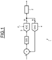
- FIG. 1 A basic diagram of a current-feedback continuous-time delta-sigma analogue/digital converter, of order one, has been represented in Figure 1 . It comprises a modulator 1 of delta-sigma type followed by a decimation digital filter 2.
- the modulator 1 is here an analogue/digital converter with oversampling and shaping of the quantization noise. It comprises an analogue/digital converter 3 (ADC) of low resolution, typically 1 bit, placed in a negative feedback loop which comprises a digital/analogue converter 4 (DAC), and whose quantization noise is rejected towards the high frequencies by virtue of a function G(f) placed in the loop.
- ADC analogue/digital converter 3
- DAC digital/analogue converter 4
- the decimation digital filter 2 makes it possible to suppress the off-band quantization noise, and to reduce the throughput of the digitized signal to the Nyquist frequency after sub-sampling, i.e. a processing frequency of the digital systems connected directly behind.
- a sinusoidal signal is used as input signal of the filter placed upstream of the modulator 1.
- This sinusoidal signal can be implemented by a square signal which is simpler to synthesize than a sinusoidal signal.
- the use of a square signal at input requires that the decimation filter 2 eliminate the harmonics which are detrimental to the precision of the attenuation measurement. This additional constraint may make it necessary to synthesize a decimation digital filter dedicated to auto-calibration. Typically, this involves a cardinal sine filter which rejects harmonics, strongly attenuating the frequencies corresponding to the frequencies of the harmonics.
- a modulator 1 of delta-sigma type comprising an analogue/digital converter 3 (ADC) and a digital/analogue converter 4 (DAC), and a decimation filter 2.
- ADC analogue/digital converter 3
- DAC digital/analogue converter 4
- the modulator 1 essentially comprises an integrator 10 carrying out the function G(f) of the negative feedback loop of Figure 1 .
- This integrator 10 comprises an operational amplifier 11 and an adjustable integration capacitance C i connected between the inverting terminal and the output terminal of the amplifier 11.
- This inverting terminal is also coupled to a resistor R 0 .
- the non-inverting terminal of the amplifier 11 is connected to earth.
- the output of the operational amplifier 11 of the integrator 10 is coupled to the converter ADC 3 which samples the output of the integrator 10 at a sampling frequency F s .
- the converter ADC 3 is coupled at output to a converter DAC 4 which is also coupled to the inverting terminal of the operational amplifier 11.
- the converter DAC 4 in this embodiment, consists of a current generator.
- the decimation filter 2 receives as input the output signal from the converter ADC 3, and controls the value of the adjustable integration capacitance C i as a function of the attenuation measured on the basis of the comparison of the measurements of powers performed.
- the modulator 1 is coupled at input to a variable-impedance filter 20 formed by a resistor R and a capacitor C.
- the variable-impedance filter 20 can consist of a variable resistance or a variable capacitor.
- the resistor R is fixed and the capacitor C is variable, so as to be in correspondence with the adjustable integration capacitance C i .
- the resistor R of the variable-impedance filter 20 may be variable, and the resistor R 0 of the modulator 1 may also be variable, it then being possible for the integration capacitance C i to be fixed.
- a controlled filter make/break switch 15 makes it possible to couple, in this embodiment, the variable capacitor C to the filter 20 and thus optionally to form the filter 20. It is thus possible for the integrated circuit 1 to control a power measurement with filter 20 or a power measurement without filter 20 by controlling the make/break switch 15.
- the decimation filter controls the value of the variable capacitor C in correspondence with the value of the integration capacitance C i , and also controls the make/break switch 15 according to the desired type of power measurement.
- an analogue input signal V in of fixed frequency At the input of the calibration system, i.e. to a terminal of the resistor R, is applied an analogue input signal V in of fixed frequency.
- the calibration of the time constant R 0 C i is generally carried out by measuring the attenuation of an ideally sinusoidal signal of fixed frequency engendered by the filter 20.
- the analogue input signal V in used in this embodiment is a square signal gated at a sub-multiple of the sampling frequency F s of the converter ADC 3. The analogy with a sinusoidal signal is then made by considering the measurements on its fundamental.
- Figure 3 presents an electronic architecture of an adjustable capacitor according to one embodiment, which can be used according to the embodiment of Figure 2 for the adjustable integration capacitance C i and the variable capacitor C of the variable-impedance filter 20.
- the adjustable capacitance comprises a fixed capacitance C f , which fixes the minimum value of the adjustable capacitance, and of at least one unit capacitance C u coupled in series with a make/break switch B.
- the fixed capacitance C f is coupled in parallel with at least one unit assembly comprising a make/break switch B and a unit capacitance C u .
- the assembly is connected between earth and the common node between the resistor R and the resistor R 0 .
- the value of the adjustable capacitance can thus be adjusted by closing the make/break switches of the unit assemblies so as to couple as many unit capacitances C u as necessary with the fixed capacitance C f to obtain the desired capacitive value.
- the precision of the value of the adjustable capacitance, and consequently the precision of the time constant R 0 C i can be modified.
- the make/break switches are controlled by digital bits arising from the decimation filter 2.
- the length of the word that is to say the number of bits of the word, corresponds to the overall number of unit capacitances C u .
- the greater the number of bits provided by the decimation filter 2 the greater the number of unit assemblies and the more the precision in the value of the time constant R 0 C i is increased.
- Figure 4 presents an electronic architecture of an adjustable resistor according to one embodiment, which can be used in the invention, according to a different embodiment from Figure 2 , for the resistor R 0 of the modulator 1 if the said resistor is embodied so as to be adjustable and for the resistor R of the variable-impedance filter 20 if said resistor is also embodied so as to be adjustable.
- the adjustable resistor comprises a fixed resistor R f , which fixes the minimum value of the adjustable resistor, and of at least one unit resistor R u coupled to a make/break switch B.
- the fixed resistor R f is wired in series with at least one unit resistor whose current input terminal is coupled to a make/break switch connected so as to short-circuit the unit resistor to which it is directly coupled at the current input of the resistor as well as all the unit resistors coupled after this make/break switch.
- the fixed resistor R f is connected to the current output terminal of the resistor R of the filter 20, while the free terminals of the make/break switches B of the resistor R 0 are wired to the modulator 1.
- the value of the adjustable resistor can thus be adjusted by opening the make/break switches so as to couple as many unit resistors R u as necessary with the fixed resistor R f to obtain the desired resistance.
- opening or closing the make/break switches B 0 , B 1 , B 2 it is possible to modify the resistance of the variable resistor.
- Figure 5 illustrates a method for calibrating the time constant RC of an integrated electronic circuit according to one mode of implementation.
- the time constant is formed by the resistance R 0 of the modulator 1 and the adjustable integration capacitance C i .
- a variable-impedance filter 20 comprising a resistor R and a variable capacitor C is coupled to the input of the modulator 1.
- the filter make/break switch 15 is opened so as to decouple the variable capacitor C from the filter 20 with a view to carrying out a power measurement without filter subsequently.
- a known analogue input signal V in of fixed frequency is applied.
- the analogue input signal V in used in this embodiment is a square signal gated at a sub-multiple of the sampling frequency F s of the converter ADC 3.
- the power at the output of the modulator 1 is measured with the aid of the decimation filter 2.
- the filter make/break switch 15 is closed (step 505) with a view to coupling the variable capacitor C of the filter 20 and thus carry out a power measurement with the filter 20.
- the same known analogue input signal V in of fixed frequency namely a square signal gated at a sub-multiple of the sampling frequency F s of the converter ADC 3, is then applied.
- the power at the output of the modulator 1 is thereafter measured with the aid of the decimation filter 2.
- a step 508 the power measurement carried out without filter 20 is compared with the power measurement carried out with the filter 20, making it possible to obtain a direct image of the analogue input signal V in attenuation engendered by the filter 20.
- a test is performed to ascertain whether the measured attenuation corresponds to the desired attenuation.
- the time constant R 0 C i corresponds to the last value applied to the adjustable integration capacitance C i (step 510).
- the decimation filter 2 chooses a lower R 0 C i pair in a step 511, before recommencing in step 505 for a new power measurement with the filter.
- the decimation filter 2 chooses a higher R 0 C i pair in a step 511 before recommencing at step 505 for a new power measurement with the filter.
- the power measurement of a continuous signal is simpler than that of a periodic signal of frequency f i . It is therefore judicious to transpose the fundamental of the square signal to the zero frequency, such as that of a continuous signal, where the power measurement corresponds to the continuous value of the transposed signal.
- the transposition is carried out by multiplying, in the time domain, the image of the fundamental of frequency f i by a sinusoid of the same frequency f i .
- the resultant is the sum of a continuous component and of a component at twice the frequency 2f i weighted by a factor of a half.
- the power measurement then corresponds to a measurement of the mean value of the signal.
- a digital integration carried out for a number N of periods and whose final value is divided by this number N.
- the division by the number N of periods can be simplified in the case where the number N is a power of two, thereby corresponding to successive shifts.
Landscapes
- Engineering & Computer Science (AREA)
- Theoretical Computer Science (AREA)
- Compression, Expansion, Code Conversion, And Decoders (AREA)
- Analogue/Digital Conversion (AREA)
- Networks Using Active Elements (AREA)
Description
- The invention relates to microelectronics, and more particularly to the calibration of a time constant RC.
- It also pertains to an integrated circuit, in particular an analogue/digital converter, provided with such a system.
- Certain signal processing functions used in analogue integrated circuits are based on the value of a time constant RC. Typically, the coefficients of an analogue filter or else of an analogue digital converter, such as a continuous-time delta-sigma analogue digital converter, are achieved by means of resistance R and capacitances C.
- The product RC of an analogue filter corresponds to its cutoff frequency. For a continuous-time delta-sigma analogue digital converter, this time constant RC is related to its sampling frequency. In both these cases, the precision of the time constant RC is important. For the cutoff frequency, if RC is estimated with too high a value, the filter cuts off a part of the signal, and if RC is too small, then the filter does not attenuate the signal sufficiently. In the case of the delta-sigma modulator, it is the performance and the stability of the modulator that depend directly on the precision of the value of RC. The RC coefficients achieve the transfer function of the current-feedback continuous-time delta-sigma analogue digital converter.
- Depending on the application, the precision with which the product RC must be known is higher or lower. A precision of the value of the time constant RC to +/-5% is generally sufficient.
- However, an integrated resistance is accurate to +/-15% while the value of an integrated capacitance varies at least by +/-20% depending on the technology. In conclusion, the time constant RC has a precision of +/-35% which is not sufficient for the great majority of applications.
- Various schemes for calibrating a time constant are already known in the prior art. Reference may be made in this regard to the documents
US 6 169 446 ,US 6 262 603 ,US 6 803 813 andUS 7 078 961 . - The calibration described in these documents is based on a comparison of the value of the time constant defined by the product RC with a known and accurate time base formulated, for example, by a quartz-driven clock, or on a comparison of the voltage across the terminals of the resistance R with that present across the terminals of the capacitance C when they are traversed by the same current.
- These schemes for calibrating the time constant RC merely deliver a digital word which directly controls a resistance or a variable capacitance.
- Moreover, they are all sensitive to the analogue imperfections intrinsic to the hardware components used to make the converter, such as the offset voltage of an operational amplifier or of the comparators used.
- Moreover it is known, in the prior art, to use a current-feedback continuous-time delta-sigma analogue digital converter coupled to a filter at input receiving a sinusoidal input signal, so as to calibrate the time constant of another current-feedback continuous-time delta-sigma analogue digital converter.
- However, the use of a second current-feedback continuous-time delta-sigma analogue digital converter is expensive in terms of time and cost.
FR 2 400 279 A
US 6 107 870 describes a method for calibrating a time constant of a filter circuit using a variable bandpass filter coupled to the same control signal and supplied with a reference signal of fixed frequency. The time constant is calibrated based on a phase shift of the reference signal engendered by the variable bandpass filter. In view of the foregoing, it is proposed to circumvent most of these limitations related to the calibration of a time constant by carrying out a measurement of a time constant of an integrated circuit of increased precision. In this respect, the invention is defined by the subject-matter of the independent claims. Advantageous embodiments are covered by the dependent claims. - In one aspect, there is proposed, according to one mode of implementation, a method for calibrating a time constant of an integrated electronic circuit.
- In this method, a variable-impedance filter is coupled at the input of the integrated electronic circuit, an analogue input signal of fixed frequency is applied to the filter, the analogue input signal attenuation engendered by the filter is measured, and the value of the time constant and the value of the impedance of the variable-impedance filter are modified until an attenuation corresponding to the desired attenuation for the integrated electronic circuit is obtained.
- Preferably, the time constant is formed by a resistive element and by a capacitive element.
- The analogue input signal attenuation engendered by the filter is determined preferably by comparing a power measurement carried out without filter with a power measurement carried out with the filter.
- The selection of measurement with and without filter can advantageously be carried out with the aid of a controlled filter make/break switch which couples the filter to the integrated circuit.
- Advantageously, the variable-impedance filter can comprise a first variable-impedance hardware component and a second variable-impedance hardware component, the first and second hardware components comprising a fixed hardware component with fixed impedance and an assembly of unit hardware components with unit impedance selectively coupled to the fixed hardware component under the control of make/break switches.
- The fixed hardware component and the unit hardware components can advantageously each comprise a resistor.
- The fixed hardware component and the unit hardware components can also each comprise a capacitor.
- Preferably, the value of the time constant is modified by generating a digital control word for operating the make/break switches, the said word corresponding to the deviation between the measured attenuation and the desired attenuation for the integrated electronic circuit.
- Each bit of the digital word generated controls a make/break switch coupling a unit assembly to a fixed hardware component of a variable-impedance hardware component. Thus, by controlling the closing or the opening of a make/break switch in accordance with the value of the bit, a unit hardware component will be coupled or decoupled to the fixed hardware component, thus modifying the impedance of the variable-impedance hardware component, and consequently the value of the time constant.
- The number of bits of the digital word and the value of the unit hardware component of a variable-impedance hardware component are thus advantageously modified as a function of a precision in the time constant.
- According to the precision required for the time constant, it is possible to modify the value of the impedance of the unit hardware components of a variable-impedance hardware component, and the number of unit assemblies. For example, by using a significant number of unit assemblies and a low impedance for the unit hardware component, the precision of the value of the impedance of the variable-impedance hardware component will be increased.
- Preferably, the analogue input signal is a square signal.
- The calibration of a time constant RC is generally carried out by measuring the attenuation of an ideally sinusoidal signal of fixed and known frequency through the cut off band of an RC filter, however, the synthesis of a sinusoidal signal is complex. In order to simplify the embodiment of the system, the input signal used during the power measurements is a square signal gated at a sub-multiple of the sampling frequency of the analogue/digital converter (ADC). The analogy with a sinusoidal signal is made by considering the measurements on its fundamental.
- Advantageously, the integrated electronic circuit (1) is a modulator of delta-sigma type.
- In another aspect, there is proposed, according to one embodiment, a system for measuring a time constant of an integrated electronic circuit.
- It comprises a variable-impedance filter coupled at the input of the integrated electronic circuit, analysis means able to measure attenuation of an analogue input signal of fixed frequency engendered by the filter and to modify the value of the time constant and the value of the impedance of the variable-impedance filter until an attenuation corresponding to the desired attenuation for the integrated electronic circuit is obtained.
- Preferably, the integrated circuit comprises a resistive element and a capacitive element forming the time constant.
- The system advantageously comprises a filter make/break switch making it possible to couple the filter to the input of the integrated circuit, the said filter make/break switch being controlled by the integrated electronic circuit.
- Advantageously, the variable-impedance filter comprises a first variable-impedance hardware component and a second variable-impedance hardware component, the first and second hardware components comprising a fixed hardware component with fixed impedance and an assembly of unit hardware components with unit impedance selectively coupled to the fixed hardware component under the control of make/break switches.
- The fixed hardware component and the unit hardware components can advantageously each comprise a resistor.
- The fixed hardware component and the unit hardware components can also each comprise a capacitor.
- Preferably, the analysis means comprise means able to generate a digital word corresponding to the deviation between the measured attenuation and the desired attenuation for the integrated electronic circuit.
- The integrated electronic circuit can advantageously comprise a modulator of delta-sigma type.
- Other advantages and characteristics of a method and system for calibration of increased precision will be apparent on examining the detailed description of wholly non-limiting embodiments, and the appended drawings, in which:
-
Figure 1 represents a basic diagram of an analogue/digital converter of delta-sigma type; -
Figure 2 presents an electronic diagram of a system for calibrating a time constant according to one embodiment; -
Figure 3 presents an electronic architecture of an adjustable capacitor according to one embodiment; -
Figure 4 presents an electronic architecture of an adjustable resistor according to one embodiment; -
Figure 5 illustrates a method for calibrating the time constant according to one mode of implementation. - Modes of implementation of a method and of a system for calibrating a time constant of an integrated circuit will be described with reference to
Figures 1 to 5 . - In the modes described, the time constant is formed by a capacitor and a resistor. Furthermore, according to the aspects described, the integrated circuit consists of a modulator of delta-sigma type.
- A basic diagram of a current-feedback continuous-time delta-sigma analogue/digital converter, of order one, has been represented in
Figure 1 . It comprises a modulator 1 of delta-sigma type followed by a decimationdigital filter 2. - The modulator 1 is here an analogue/digital converter with oversampling and shaping of the quantization noise. It comprises an analogue/digital converter 3 (ADC) of low resolution, typically 1 bit, placed in a negative feedback loop which comprises a digital/analogue converter 4 (DAC), and whose quantization noise is rejected towards the high frequencies by virtue of a function G(f) placed in the loop.
- The decimation
digital filter 2 makes it possible to suppress the off-band quantization noise, and to reduce the throughput of the digitized signal to the Nyquist frequency after sub-sampling, i.e. a processing frequency of the digital systems connected directly behind. - Ideally, a sinusoidal signal is used as input signal of the filter placed upstream of the modulator 1. This sinusoidal signal can be implemented by a square signal which is simpler to synthesize than a sinusoidal signal. The use of a square signal at input requires that the
decimation filter 2 eliminate the harmonics which are detrimental to the precision of the attenuation measurement. This additional constraint may make it necessary to synthesize a decimation digital filter dedicated to auto-calibration. Typically, this involves a cardinal sine filter which rejects harmonics, strongly attenuating the frequencies corresponding to the frequencies of the harmonics. - The performance of such a delta-sigma modulator 1 depends on the over-sampling ratio, the number of bits N of the ADC/DAC pair and the order of the loop filter G(f).
- Based on the principle described in
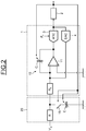
Figure 1 , an embodiment of a system for calibrating a time constant RC formed by the association of a resistor R and of a capacitor C has been detailed inFigure 2 . - It comprises, as in the example of
Figure 1 , a modulator 1 of delta-sigma type comprising an analogue/digital converter 3 (ADC) and a digital/analogue converter 4 (DAC), and adecimation filter 2. - The modulator 1 essentially comprises an
integrator 10 carrying out the function G(f) of the negative feedback loop ofFigure 1 . Thisintegrator 10 comprises anoperational amplifier 11 and an adjustable integration capacitance Ci connected between the inverting terminal and the output terminal of theamplifier 11. This inverting terminal is also coupled to a resistor R0. The non-inverting terminal of theamplifier 11 is connected to earth. - The output of the
operational amplifier 11 of theintegrator 10 is coupled to theconverter ADC 3 which samples the output of theintegrator 10 at a sampling frequency Fs. Theconverter ADC 3 is coupled at output to aconverter DAC 4 which is also coupled to the inverting terminal of theoperational amplifier 11. - The
converter DAC 4, in this embodiment, consists of a current generator. - The
decimation filter 2 receives as input the output signal from theconverter ADC 3, and controls the value of the adjustable integration capacitance Ci as a function of the attenuation measured on the basis of the comparison of the measurements of powers performed. - The modulator 1 is coupled at input to a variable-
impedance filter 20 formed by a resistor R and a capacitor C. The variable-impedance filter 20 can consist of a variable resistance or a variable capacitor. In this embodiment, the resistor R is fixed and the capacitor C is variable, so as to be in correspondence with the adjustable integration capacitance Ci. - It should be noted that the resistor R of the variable-
impedance filter 20 may be variable, and the resistor R0 of the modulator 1 may also be variable, it then being possible for the integration capacitance Ci to be fixed. - A controlled filter make/break
switch 15 makes it possible to couple, in this embodiment, the variable capacitor C to thefilter 20 and thus optionally to form thefilter 20. It is thus possible for the integrated circuit 1 to control a power measurement withfilter 20 or a power measurement withoutfilter 20 by controlling the make/breakswitch 15. - The decimation filter controls the value of the variable capacitor C in correspondence with the value of the integration capacitance Ci, and also controls the make/break
switch 15 according to the desired type of power measurement. - At the input of the calibration system, i.e. to a terminal of the resistor R, is applied an analogue input signal Vin of fixed frequency. The calibration of the time constant R0Ci is generally carried out by measuring the attenuation of an ideally sinusoidal signal of fixed frequency engendered by the
filter 20. In order to simplify the embodiment of the system, the analogue input signal Vin used in this embodiment is a square signal gated at a sub-multiple of the sampling frequency Fs of theconverter ADC 3. The analogy with a sinusoidal signal is then made by considering the measurements on its fundamental. -
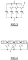
Figure 3 presents an electronic architecture of an adjustable capacitor according to one embodiment, which can be used according to the embodiment ofFigure 2 for the adjustable integration capacitance Ci and the variable capacitor C of the variable-impedance filter 20. - The adjustable capacitance comprises a fixed capacitance Cf, which fixes the minimum value of the adjustable capacitance, and of at least one unit capacitance Cu coupled in series with a make/break switch B. The fixed capacitance Cf is coupled in parallel with at least one unit assembly comprising a make/break switch B and a unit capacitance Cu. For example, for the embodiment of the adjustable capacitor C, the assembly is connected between earth and the common node between the resistor R and the resistor R0. The value of the adjustable capacitance can thus be adjusted by closing the make/break switches of the unit assemblies so as to couple as many unit capacitances Cu as necessary with the fixed capacitance Cf to obtain the desired capacitive value. Thus, according to one embodiment, by opening or closing the make/break switches B0, B1, B2, it is possible to modify the value of the variable capacitance, by coupling or decoupling unit capacitances Cu to the fixed capacitance Cf.
- According to the value of the unit capacitances, and according to the number of unit assemblies available, the precision of the value of the adjustable capacitance, and consequently the precision of the time constant R0Ci, can be modified.
- The make/break switches are controlled by digital bits arising from the
decimation filter 2. Of course, the length of the word, that is to say the number of bits of the word, corresponds to the overall number of unit capacitances Cu. Thus, the greater the number of bits provided by thedecimation filter 2, the greater the number of unit assemblies and the more the precision in the value of the time constant R0Ci is increased. -
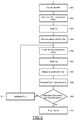
Figure 4 presents an electronic architecture of an adjustable resistor according to one embodiment, which can be used in the invention, according to a different embodiment fromFigure 2 , for the resistor R0 of the modulator 1 if the said resistor is embodied so as to be adjustable and for the resistor R of the variable-impedance filter 20 if said resistor is also embodied so as to be adjustable. - The adjustable resistor comprises a fixed resistor Rf, which fixes the minimum value of the adjustable resistor, and of at least one unit resistor Ru coupled to a make/break switch B. The fixed resistor Rf is wired in series with at least one unit resistor whose current input terminal is coupled to a make/break switch connected so as to short-circuit the unit resistor to which it is directly coupled at the current input of the resistor as well as all the unit resistors coupled after this make/break switch.
- For example, when this arrangement is intended to form the adjustable resistor R0, the fixed resistor Rf is connected to the current output terminal of the resistor R of the
filter 20, while the free terminals of the make/break switches B of the resistor R0 are wired to the modulator 1. - The value of the adjustable resistor can thus be adjusted by opening the make/break switches so as to couple as many unit resistors Ru as necessary with the fixed resistor Rf to obtain the desired resistance. Thus, according to one embodiment, by opening or closing the make/break switches
B 0 ,B 1 ,B 2 , it is possible to modify the resistance of the variable resistor. -
Figure 5 illustrates a method for calibrating the time constant RC of an integrated electronic circuit according to one mode of implementation. According to this mode of implementation, the time constant is formed by the resistance R0 of the modulator 1 and the adjustable integration capacitance Ci. - In a
first step 501, and also referring toFigure 2 , a variable-impedance filter 20 comprising a resistor R and a variable capacitor C is coupled to the input of the modulator 1. In a followingstep 502, the filter make/breakswitch 15 is opened so as to decouple the variable capacitor C from thefilter 20 with a view to carrying out a power measurement without filter subsequently. In athird step 503, a known analogue input signal Vin of fixed frequency is applied. The analogue input signal Vin used in this embodiment is a square signal gated at a sub-multiple of the sampling frequency Fs of theconverter ADC 3. In a followingstep 504, the power at the output of the modulator 1 is measured with the aid of thedecimation filter 2. - Secondly, the filter make/break
switch 15 is closed (step 505) with a view to coupling the variable capacitor C of thefilter 20 and thus carry out a power measurement with thefilter 20. In astep 506, the same known analogue input signal Vin of fixed frequency, namely a square signal gated at a sub-multiple of the sampling frequency Fs of theconverter ADC 3, is then applied. In astep 507, the power at the output of the modulator 1 is thereafter measured with the aid of thedecimation filter 2. - Thirdly, in a
step 508, the power measurement carried out withoutfilter 20 is compared with the power measurement carried out with thefilter 20, making it possible to obtain a direct image of the analogue input signal Vin attenuation engendered by thefilter 20. In astep 509, a test is performed to ascertain whether the measured attenuation corresponds to the desired attenuation. - When the measured attenuation corresponds to the desired attenuation, it is considered that the time constant R0Ci corresponds to the last value applied to the adjustable integration capacitance Ci (step 510).
- When the attenuation is too high, the R0Ci pair is too high and the corresponding cutoff frequency fc is too low. The
decimation filter 2 then chooses a lower R0Ci pair in astep 511, before recommencing instep 505 for a new power measurement with the filter. - As a reminder, the cutoff frequency is expressed according to the following expression:

- When on the other hand the attenuation is too low, the R0Ci pair is too low and the cutoff frequency fc is too high. The
decimation filter 2 then chooses a higher R0Ci pair in astep 511 before recommencing atstep 505 for a new power measurement with the filter. - It should be noted that the power measurement of a continuous signal is simpler than that of a periodic signal of frequency fi. It is therefore judicious to transpose the fundamental of the square signal to the zero frequency, such as that of a continuous signal, where the power measurement corresponds to the continuous value of the transposed signal. The transposition is carried out by multiplying, in the time domain, the image of the fundamental of frequency fi by a sinusoid of the same frequency fi. The resultant is the sum of a continuous component and of a component at twice the frequency 2fi weighted by a factor of a half.
- In continuous mode, the power measurement then corresponds to a measurement of the mean value of the signal. Such an operation is achievable with a digital integration carried out for a number N of periods and whose final value is divided by this number N. Over this number N of periods, the z-transfer function of the mean is as follows:

- The division by the number N of periods can be simplified in the case where the number N is a power of two, thereby corresponding to successive shifts.
- There is therefore proposed, according to the present description, the use of an integrated electronic circuit, in particular a current-feedback continuous-time delta-sigma converter, making it possible to provide an autocalibration of the time constant R0Ci of this same current-feedback continuous-time delta-sigma converter, on the basis of a measurement of the attenuation of a square analogue input signal of fixed frequency through the cut off band of a filter coupled at the input of the delta-sigma converter. By comparing a power measurement without filter with a power measurement with the filter, the measured attenuation is determined and is compared with the desired attenuation. The value of the time constant R0Ci and the value of the filter are then modified in correspondence until the desired attenuation is obtained.
Claims (17)
- Method for calibrating an adjustable time constant (R0Ci) of an integrated electronic circuit (1), the method comprising a step (501) of coupling a variable-impedance filter (20) at an input of the integrated electronic circuit (1), a step (506) of applying an analogue input signal (Vin) of fixed frequency to the variable-impedance filter (20), a step (507) of measuring the analogue input signal (Vin) attenuation engendered by the variable-impedance filter (20), and a step (511) of modifying the value of the time constant (R0Ci) and the value of the impedance of the variable-impedance filter (20) in correspondence until the measured attenuation corresponds to a desired attenuation for the integrated electronic circuit (1), the analogue input signal (Vin) attenuation engendered by the variable-impedance filter (20) being determined by comparing (508) a power measurement carried out without the variable-impedance filter (20) with a power measurement carried out with the variable-impedance filter (20).
- Method according to Claim 1, in which the time constant (R0Ci) is formed by a resistive element (Ro) and by a capacitive element (Ci).
- Method according to Claim 1 or 2, in which the measurement selection with and without the variable-impedance filter (20) is carried out with the aid of a controlled filter make/break switch (15) which couples the variable-impedance (20) to the integrated circuit (1).
- Method in accordance with one of Claims 1 to 3, in which the variable-impedance filter (20) comprises a first variable-impedance hardware component and a second variable-impedance hardware component, the first and second hardware components comprising a fixed hardware component with fixed impedance and an assembly of unit hardware components with unit impedance selectively coupled to the fixed hardware component under the control of make/break switches (B).
- Method according to Claim 4, in which the fixed hardware component and the unit hardware components each comprise a resistor.
- Method according to Claim 4, in which the fixed hardware component and the unit hardware components each comprise a capacitor.
- Method according to one of Claims 4 to 6, in which the value of the time constant (R0Ci) is modified by generating a digital control word for operating the make/break switches, the said word corresponding to the deviation between the measured attenuation and the desired attenuation for the integrated electronic circuit (1).
- Method according to Claim 7, in which the number of bits of the digital word and the value of the unit hardware component of a variable- impedance hardware component are modified as a function of a precision in the time constant (R0Ci).
- Method according to one of Claims 1 to 8, in which the analogue input signal (Vin) is a square signal.
- Method according to one of Claims 1 to 9, in which the integrated electronic circuit (1) is a modulator of delta-sigma type.
- System for calibrating a time constant (R0Ci) of an integrated electronic circuit (1), comprising:an integrated electronic circuit (1) with time constant (R0Ci), a variable-impedance filter (20) coupled at an input of the integrated electronic circuit (1),analysis means adapted to measure the attenuation of an analogue input signal (Vin) of fixed frequency engendered by the variable-impedance filter (20) and to modify the value of the time constant (R0Ci) and the value of the impedance of the variable-impedance filter (20) in correspondence until the measured attenuation corresponds to the desired attenuation for the integrated electronic circuit (1), anda filter make/break switch (15) adapted to couple the variable-impedance filter (20) to the input of the integrated circuit (1), the said filter make/break switch (15) being controlled by the integrated circuit (1), and whereinthe analogue input signal (Vin) attenuation engendered by the variable-impedance filter (20) is determined by comparing a power measurement carried out without the variable-impedance filter (20) with a power measurement carried out with the variable-impedance filter (20).
- System according to Claim 11, wherein the integrated circuit (1) comprises a resistive element (R0) and a capacitive element (Cj) forming the time constant (R0Ci).
- System according to one of Claims 11 or 12, wherein the variable-impedance filter (20) comprises a first variable-impedance hardware component and a second variable-impedance hardware component, the first and second hardware components comprising a fixed hardware component with fixed impedance and an assembly of unit hardware components with unit impedance selectively coupled to the fixed hardware component under the control of make/break switches (B).
- System according to Claim 13, wherein the fixed hardware component and the unit hardware components each comprise a resistor.
- System according to Claim 13, wherein the fixed hardware component and the unit hardware components each comprise a capacitor.
- System according to one of Claims 11 to 15, in which the analysis means comprise means able to generate a digital control word for operating the make/break switches, the said word corresponding to the deviation between the measured attenuation and the desired attenuation for the integrated electronic circuit (1).
- System according to one of Claims 11 to 16, wherein the integrated electronic circuit (1) comprises a modulator of delta-sigma type.
Applications Claiming Priority (2)
| Application Number | Priority Date | Filing Date | Title |
|---|---|---|---|
| FR0950523A FR2941576B1 (en) | 2009-01-28 | 2009-01-28 | METHOD AND SYSTEM FOR CALIBRATING AN INTEGRATED TIME CONSTANT, AND INTEGRATED CIRCUIT PROVIDED WITH SUCH A SYSTEM |
| PCT/EP2010/050965 WO2010086347A2 (en) | 2009-01-28 | 2010-01-28 | System for calibrating a time constant of an integrated circuit, and integrated circuit provided with such a system. |
Publications (2)
| Publication Number | Publication Date |
|---|---|
| EP2382708A2 EP2382708A2 (en) | 2011-11-02 |
| EP2382708B1 true EP2382708B1 (en) | 2017-12-27 |
Family
ID=40690318
Family Applications (1)
| Application Number | Title | Priority Date | Filing Date |
|---|---|---|---|
| EP10701528.1A Not-in-force EP2382708B1 (en) | 2009-01-28 | 2010-01-28 | System for calibrating a time constant of an integrated circuit, and integrated circuit provided with such a system. |
Country Status (5)
| Country | Link |
|---|---|
| US (1) | US8610610B2 (en) |
| EP (1) | EP2382708B1 (en) |
| CN (1) | CN102301591B (en) |
| FR (1) | FR2941576B1 (en) |
| WO (1) | WO2010086347A2 (en) |
Families Citing this family (2)
| Publication number | Priority date | Publication date | Assignee | Title |
|---|---|---|---|---|
| DE102013223394B4 (en) * | 2013-11-15 | 2015-07-16 | Fraunhofer-Gesellschaft zur Förderung der angewandten Forschung e.V. | Electrical circuit |
| WO2016203522A1 (en) * | 2015-06-15 | 2016-12-22 | オリンパス株式会社 | Successive approximation a/d converter |
Citations (1)
| Publication number | Priority date | Publication date | Assignee | Title |
|---|---|---|---|---|
| US6107870A (en) * | 1997-10-16 | 2000-08-22 | Kabushiki Kaisha Toshiba | Automatic compensation circuit for automatically compensating time constant of filter |
Family Cites Families (13)
| Publication number | Priority date | Publication date | Assignee | Title |
|---|---|---|---|---|
| US3914694A (en) * | 1973-09-12 | 1975-10-21 | Sun Oil Co Pennsylvania | Frequency modulation circuit |
| US3940715A (en) * | 1974-09-25 | 1976-02-24 | Sound Technology, Inc. | Distortion measurement system |
| FR2400279A1 (en) * | 1977-08-09 | 1979-03-09 | Simeau Bernard | SIGNAL ANALYSIS AND PROCESSING DEVICES |
| US4730499A (en) * | 1986-11-04 | 1988-03-15 | The Perkin-Elmer Corporation | Measurement of flow rate of powder from a hopper |
| US5392456A (en) * | 1989-10-06 | 1995-02-21 | Hitachi, Ltd. | Method of controlling filter time constant and filter circuit having the time constant control function based on the method |
| FR2775141B1 (en) | 1998-02-19 | 2002-10-11 | Sgs Thomson Microelectronics | TIME CONSTANT CALIBRATION DEVICE |
| US6262603B1 (en) | 2000-02-29 | 2001-07-17 | National Semiconductor Corporation | RC calibration circuit with reduced power consumption and increased accuracy |
| US6622103B1 (en) * | 2000-06-20 | 2003-09-16 | Formfactor, Inc. | System for calibrating timing of an integrated circuit wafer tester |
| JP4098701B2 (en) * | 2002-12-27 | 2008-06-11 | 株式会社東芝 | Variable time constant circuit and filter circuit using the same |
| US7002417B2 (en) * | 2003-03-21 | 2006-02-21 | Nokia Corporation | RC and SC filter compensation in a radio transceiver |
| US6803813B1 (en) | 2003-04-22 | 2004-10-12 | National Semiconductor Corporation | Time constant-based calibration circuit for active filters |
| DE10321200B3 (en) | 2003-05-12 | 2005-02-03 | Infineon Technologies Ag | Apparatus and method for calibrating R / C filter circuits |
| US8462030B2 (en) * | 2004-04-27 | 2013-06-11 | Texas Instruments Incorporated | Programmable loop filter for use with a sigma delta analog-to-digital converter and method of programming the same |
-
2009
- 2009-01-28 FR FR0950523A patent/FR2941576B1/en not_active Expired - Fee Related
-
2010
- 2010-01-28 CN CN201080005906.2A patent/CN102301591B/en not_active Expired - Fee Related
- 2010-01-28 WO PCT/EP2010/050965 patent/WO2010086347A2/en not_active Ceased
- 2010-01-28 EP EP10701528.1A patent/EP2382708B1/en not_active Not-in-force
- 2010-01-28 US US13/146,898 patent/US8610610B2/en not_active Expired - Fee Related
Patent Citations (1)
| Publication number | Priority date | Publication date | Assignee | Title |
|---|---|---|---|---|
| US6107870A (en) * | 1997-10-16 | 2000-08-22 | Kabushiki Kaisha Toshiba | Automatic compensation circuit for automatically compensating time constant of filter |
Also Published As
| Publication number | Publication date |
|---|---|
| FR2941576B1 (en) | 2016-07-15 |
| US8610610B2 (en) | 2013-12-17 |
| US20120026024A1 (en) | 2012-02-02 |
| CN102301591B (en) | 2015-04-29 |
| FR2941576A1 (en) | 2010-07-30 |
| WO2010086347A3 (en) | 2010-12-23 |
| WO2010086347A2 (en) | 2010-08-05 |
| CN102301591A (en) | 2011-12-28 |
| EP2382708A2 (en) | 2011-11-02 |
Similar Documents
| Publication | Publication Date | Title |
|---|---|---|
| Norsworthy et al. | A 14-bit 80-kHz sigma-delta A/D converter: modeling, design and performance evaluation | |
| US9459298B2 (en) | Method and apparatus for sensing capacitance value and converting it into digital format | |
| CN100523832C (en) | Method and apparatus for phase compensation in an electronic energy meter | |
| US20140375374A1 (en) | Capacitance to Digital Converter and Method | |
| Dallet et al. | Dynamic characterisation of analogue-to-digital converters | |
| JPH06249889A (en) | Voltage and current measuring unit and voltage and current measuring method | |
| US6781361B2 (en) | Apparatus and system for electrical power metering using digital integration | |
| US7193546B1 (en) | Phase-measuring delta-sigma modulator calibration method and apparatus | |
| JP2999468B2 (en) | Method and apparatus for discrete time measurement of reactance | |
| US8610610B2 (en) | System for calibrating a time constant of an integrated circuit, and integrated circuit provided with such a system | |
| EP2382709B1 (en) | Method and system for measuring a time constant of an integrated circuit, and integrated circuit provided with such a system | |
| EP0862060A2 (en) | RMS converter using digital filtering | |
| US20060028197A1 (en) | Direct current offset cancellation and phase equalization for power metering devices | |
| Grimaldi et al. | Identification of ADC error model by testing of the chosen code bins | |
| US20040189326A1 (en) | Vector-detecting apparatus and impedance measuring apparatus | |
| Brennan | Measuring a Loudspeaker Impedance Profile Using the AD5933 | |
| CN111487476B (en) | Quasi-peak detection method and quasi-peak detector | |
| US20260133231A1 (en) | Single pin impedance measurement system and phase offset compensation for a single pin impedance measurement system | |
| Leis | Lock-in amplification based on sigma-delta oversampling | |
| MatiC et al. | Comparison of digital signal processing methods for sine wave signal generation | |
| EP1008861A1 (en) | AC calibration apparatus | |
| Michaeli et al. | Fast testing of ADC using unified error model | |
| Hong et al. | A built-in-self-test Σ-Δ ADC prototype | |
| ADCs | SECTION 3 HIGH RESOLUTION SIGNAL CONDITIONING ADCs | |
| Devices | Mixed-signal and DSP design techniques |
Legal Events
| Date | Code | Title | Description |
|---|---|---|---|
| PUAI | Public reference made under article 153(3) epc to a published international application that has entered the european phase |
Free format text: ORIGINAL CODE: 0009012 |
|
| 17P | Request for examination filed |
Effective date: 20110627 |
|
| AK | Designated contracting states |
Kind code of ref document: A2 Designated state(s): AT BE BG CH CY CZ DE DK EE ES FI FR GB GR HR HU IE IS IT LI LT LU LV MC MK MT NL NO PL PT RO SE SI SK SM TR |
|
| DAX | Request for extension of the european patent (deleted) | ||
| 17Q | First examination report despatched |
Effective date: 20161013 |
|
| RAP1 | Party data changed (applicant data changed or rights of an application transferred) |
Owner name: OCT CIRCUIT TECHNOLOGIES INTERNATIONAL LIMITED |
|
| REG | Reference to a national code |
Ref country code: DE Ref legal event code: R079 Ref document number: 602010047621 Country of ref document: DE Free format text: PREVIOUS MAIN CLASS: H03H0011120000 Ipc: H03H0007010000 |
|
| GRAP | Despatch of communication of intention to grant a patent |
Free format text: ORIGINAL CODE: EPIDOSNIGR1 |
|
| RIC1 | Information provided on ipc code assigned before grant |
Ipc: H03M 3/00 20060101ALI20170531BHEP Ipc: H03H 11/12 20060101ALI20170531BHEP Ipc: H03H 7/01 20060101AFI20170531BHEP |
|
| INTG | Intention to grant announced |
Effective date: 20170704 |
|
| RIN1 | Information on inventor provided before grant (corrected) |
Inventor name: AMIACH, JONATHAN Inventor name: LEFEBVRE, SEBASTIEN Inventor name: ANDRE, ERIC |
|
| GRAS | Grant fee paid |
Free format text: ORIGINAL CODE: EPIDOSNIGR3 |
|
| GRAA | (expected) grant |
Free format text: ORIGINAL CODE: 0009210 |
|
| AK | Designated contracting states |
Kind code of ref document: B1 Designated state(s): AT BE BG CH CY CZ DE DK EE ES FI FR GB GR HR HU IE IS IT LI LT LU LV MC MK MT NL NO PL PT RO SE SI SK SM TR |
|
| REG | Reference to a national code |
Ref country code: GB Ref legal event code: FG4D |
|
| REG | Reference to a national code |
Ref country code: CH Ref legal event code: EP |
|
| REG | Reference to a national code |
Ref country code: AT Ref legal event code: REF Ref document number: 959104 Country of ref document: AT Kind code of ref document: T Effective date: 20180115 |
|
| REG | Reference to a national code |
Ref country code: IE Ref legal event code: FG4D |
|
| REG | Reference to a national code |
Ref country code: DE Ref legal event code: R096 Ref document number: 602010047621 Country of ref document: DE |
|
| PG25 | Lapsed in a contracting state [announced via postgrant information from national office to epo] |
Ref country code: NO Free format text: LAPSE BECAUSE OF FAILURE TO SUBMIT A TRANSLATION OF THE DESCRIPTION OR TO PAY THE FEE WITHIN THE PRESCRIBED TIME-LIMIT Effective date: 20180327 Ref country code: LT Free format text: LAPSE BECAUSE OF FAILURE TO SUBMIT A TRANSLATION OF THE DESCRIPTION OR TO PAY THE FEE WITHIN THE PRESCRIBED TIME-LIMIT Effective date: 20171227 Ref country code: FI Free format text: LAPSE BECAUSE OF FAILURE TO SUBMIT A TRANSLATION OF THE DESCRIPTION OR TO PAY THE FEE WITHIN THE PRESCRIBED TIME-LIMIT Effective date: 20171227 |
|
| REG | Reference to a national code |
Ref country code: NL Ref legal event code: MP Effective date: 20171227 |
|
| REG | Reference to a national code |
Ref country code: LT Ref legal event code: MG4D |
|
| REG | Reference to a national code |
Ref country code: AT Ref legal event code: MK05 Ref document number: 959104 Country of ref document: AT Kind code of ref document: T Effective date: 20171227 |
|
| PG25 | Lapsed in a contracting state [announced via postgrant information from national office to epo] |
Ref country code: LV Free format text: LAPSE BECAUSE OF FAILURE TO SUBMIT A TRANSLATION OF THE DESCRIPTION OR TO PAY THE FEE WITHIN THE PRESCRIBED TIME-LIMIT Effective date: 20171227 Ref country code: GR Free format text: LAPSE BECAUSE OF FAILURE TO SUBMIT A TRANSLATION OF THE DESCRIPTION OR TO PAY THE FEE WITHIN THE PRESCRIBED TIME-LIMIT Effective date: 20180328 Ref country code: HR Free format text: LAPSE BECAUSE OF FAILURE TO SUBMIT A TRANSLATION OF THE DESCRIPTION OR TO PAY THE FEE WITHIN THE PRESCRIBED TIME-LIMIT Effective date: 20171227 Ref country code: BG Free format text: LAPSE BECAUSE OF FAILURE TO SUBMIT A TRANSLATION OF THE DESCRIPTION OR TO PAY THE FEE WITHIN THE PRESCRIBED TIME-LIMIT Effective date: 20180327 |
|
| PG25 | Lapsed in a contracting state [announced via postgrant information from national office to epo] |
Ref country code: NL Free format text: LAPSE BECAUSE OF FAILURE TO SUBMIT A TRANSLATION OF THE DESCRIPTION OR TO PAY THE FEE WITHIN THE PRESCRIBED TIME-LIMIT Effective date: 20171227 |
|
| PG25 | Lapsed in a contracting state [announced via postgrant information from national office to epo] |
Ref country code: ES Free format text: LAPSE BECAUSE OF FAILURE TO SUBMIT A TRANSLATION OF THE DESCRIPTION OR TO PAY THE FEE WITHIN THE PRESCRIBED TIME-LIMIT Effective date: 20171227 Ref country code: EE Free format text: LAPSE BECAUSE OF FAILURE TO SUBMIT A TRANSLATION OF THE DESCRIPTION OR TO PAY THE FEE WITHIN THE PRESCRIBED TIME-LIMIT Effective date: 20171227 Ref country code: CY Free format text: LAPSE BECAUSE OF FAILURE TO SUBMIT A TRANSLATION OF THE DESCRIPTION OR TO PAY THE FEE WITHIN THE PRESCRIBED TIME-LIMIT Effective date: 20171227 Ref country code: CZ Free format text: LAPSE BECAUSE OF FAILURE TO SUBMIT A TRANSLATION OF THE DESCRIPTION OR TO PAY THE FEE WITHIN THE PRESCRIBED TIME-LIMIT Effective date: 20171227 Ref country code: SK Free format text: LAPSE BECAUSE OF FAILURE TO SUBMIT A TRANSLATION OF THE DESCRIPTION OR TO PAY THE FEE WITHIN THE PRESCRIBED TIME-LIMIT Effective date: 20171227 |
|
| PG25 | Lapsed in a contracting state [announced via postgrant information from national office to epo] |
Ref country code: SM Free format text: LAPSE BECAUSE OF FAILURE TO SUBMIT A TRANSLATION OF THE DESCRIPTION OR TO PAY THE FEE WITHIN THE PRESCRIBED TIME-LIMIT Effective date: 20171227 Ref country code: IT Free format text: LAPSE BECAUSE OF FAILURE TO SUBMIT A TRANSLATION OF THE DESCRIPTION OR TO PAY THE FEE WITHIN THE PRESCRIBED TIME-LIMIT Effective date: 20171227 Ref country code: AT Free format text: LAPSE BECAUSE OF FAILURE TO SUBMIT A TRANSLATION OF THE DESCRIPTION OR TO PAY THE FEE WITHIN THE PRESCRIBED TIME-LIMIT Effective date: 20171227 Ref country code: RO Free format text: LAPSE BECAUSE OF FAILURE TO SUBMIT A TRANSLATION OF THE DESCRIPTION OR TO PAY THE FEE WITHIN THE PRESCRIBED TIME-LIMIT Effective date: 20171227 Ref country code: IS Free format text: LAPSE BECAUSE OF FAILURE TO SUBMIT A TRANSLATION OF THE DESCRIPTION OR TO PAY THE FEE WITHIN THE PRESCRIBED TIME-LIMIT Effective date: 20180427 Ref country code: PL Free format text: LAPSE BECAUSE OF FAILURE TO SUBMIT A TRANSLATION OF THE DESCRIPTION OR TO PAY THE FEE WITHIN THE PRESCRIBED TIME-LIMIT Effective date: 20171227 |
|
| REG | Reference to a national code |
Ref country code: CH Ref legal event code: PL |
|
| PG25 | Lapsed in a contracting state [announced via postgrant information from national office to epo] |
Ref country code: MC Free format text: LAPSE BECAUSE OF FAILURE TO SUBMIT A TRANSLATION OF THE DESCRIPTION OR TO PAY THE FEE WITHIN THE PRESCRIBED TIME-LIMIT Effective date: 20171227 |
|
| REG | Reference to a national code |
Ref country code: DE Ref legal event code: R097 Ref document number: 602010047621 Country of ref document: DE |
|
| PG25 | Lapsed in a contracting state [announced via postgrant information from national office to epo] |
Ref country code: FR Free format text: LAPSE BECAUSE OF NON-PAYMENT OF DUE FEES Effective date: 20180227 Ref country code: LU Free format text: LAPSE BECAUSE OF NON-PAYMENT OF DUE FEES Effective date: 20180128 |
|
| REG | Reference to a national code |
Ref country code: IE Ref legal event code: MM4A |
|
| PLBE | No opposition filed within time limit |
Free format text: ORIGINAL CODE: 0009261 |
|
| REG | Reference to a national code |
Ref country code: FR Ref legal event code: ST Effective date: 20180928 |
|
| STAA | Information on the status of an ep patent application or granted ep patent |
Free format text: STATUS: NO OPPOSITION FILED WITHIN TIME LIMIT |
|
| REG | Reference to a national code |
Ref country code: BE Ref legal event code: MM Effective date: 20180131 |
|
| GBPC | Gb: european patent ceased through non-payment of renewal fee |
Effective date: 20180327 |
|
| PG25 | Lapsed in a contracting state [announced via postgrant information from national office to epo] |
Ref country code: DK Free format text: LAPSE BECAUSE OF FAILURE TO SUBMIT A TRANSLATION OF THE DESCRIPTION OR TO PAY THE FEE WITHIN THE PRESCRIBED TIME-LIMIT Effective date: 20171227 Ref country code: BE Free format text: LAPSE BECAUSE OF NON-PAYMENT OF DUE FEES Effective date: 20180131 Ref country code: CH Free format text: LAPSE BECAUSE OF NON-PAYMENT OF DUE FEES Effective date: 20180131 Ref country code: LI Free format text: LAPSE BECAUSE OF NON-PAYMENT OF DUE FEES Effective date: 20180131 |
|
| 26N | No opposition filed |
Effective date: 20180928 |
|
| PG25 | Lapsed in a contracting state [announced via postgrant information from national office to epo] |
Ref country code: IE Free format text: LAPSE BECAUSE OF NON-PAYMENT OF DUE FEES Effective date: 20180128 |
|
| PG25 | Lapsed in a contracting state [announced via postgrant information from national office to epo] |
Ref country code: SI Free format text: LAPSE BECAUSE OF FAILURE TO SUBMIT A TRANSLATION OF THE DESCRIPTION OR TO PAY THE FEE WITHIN THE PRESCRIBED TIME-LIMIT Effective date: 20171227 Ref country code: GB Free format text: LAPSE BECAUSE OF NON-PAYMENT OF DUE FEES Effective date: 20180327 |
|
| PG25 | Lapsed in a contracting state [announced via postgrant information from national office to epo] |
Ref country code: MT Free format text: LAPSE BECAUSE OF NON-PAYMENT OF DUE FEES Effective date: 20180128 |
|
| PG25 | Lapsed in a contracting state [announced via postgrant information from national office to epo] |
Ref country code: TR Free format text: LAPSE BECAUSE OF FAILURE TO SUBMIT A TRANSLATION OF THE DESCRIPTION OR TO PAY THE FEE WITHIN THE PRESCRIBED TIME-LIMIT Effective date: 20171227 |
|
| PG25 | Lapsed in a contracting state [announced via postgrant information from national office to epo] |
Ref country code: HU Free format text: LAPSE BECAUSE OF FAILURE TO SUBMIT A TRANSLATION OF THE DESCRIPTION OR TO PAY THE FEE WITHIN THE PRESCRIBED TIME-LIMIT; INVALID AB INITIO Effective date: 20100128 Ref country code: PT Free format text: LAPSE BECAUSE OF FAILURE TO SUBMIT A TRANSLATION OF THE DESCRIPTION OR TO PAY THE FEE WITHIN THE PRESCRIBED TIME-LIMIT Effective date: 20171227 |
|
| PG25 | Lapsed in a contracting state [announced via postgrant information from national office to epo] |
Ref country code: SE Free format text: LAPSE BECAUSE OF FAILURE TO SUBMIT A TRANSLATION OF THE DESCRIPTION OR TO PAY THE FEE WITHIN THE PRESCRIBED TIME-LIMIT Effective date: 20171227 Ref country code: MK Free format text: LAPSE BECAUSE OF NON-PAYMENT OF DUE FEES Effective date: 20171227 |
|
| PGFP | Annual fee paid to national office [announced via postgrant information from national office to epo] |
Ref country code: DE Payment date: 20210127 Year of fee payment: 12 |
|
| REG | Reference to a national code |
Ref country code: DE Ref legal event code: R119 Ref document number: 602010047621 Country of ref document: DE |
|
| PG25 | Lapsed in a contracting state [announced via postgrant information from national office to epo] |
Ref country code: DE Free format text: LAPSE BECAUSE OF NON-PAYMENT OF DUE FEES Effective date: 20220802 |