EP2378425A1 - A testing system for integrated circuits - Google Patents
A testing system for integrated circuits Download PDFInfo
- Publication number
- EP2378425A1 EP2378425A1 EP11160477A EP11160477A EP2378425A1 EP 2378425 A1 EP2378425 A1 EP 2378425A1 EP 11160477 A EP11160477 A EP 11160477A EP 11160477 A EP11160477 A EP 11160477A EP 2378425 A1 EP2378425 A1 EP 2378425A1
- Authority
- EP
- European Patent Office
- Prior art keywords
- clock
- flop
- test
- flip
- signal
- Prior art date
- Legal status (The legal status is an assumption and is not a legal conclusion. Google has not performed a legal analysis and makes no representation as to the accuracy of the status listed.)
- Withdrawn
Links
- 238000012360 testing method Methods 0.000 title claims abstract description 52
- 238000000034 method Methods 0.000 description 10
- 238000011144 upstream manufacturing Methods 0.000 description 5
- 238000010586 diagram Methods 0.000 description 3
- 230000015572 biosynthetic process Effects 0.000 description 2
- 238000013461 design Methods 0.000 description 2
- 238000011161 development Methods 0.000 description 2
- 238000004519 manufacturing process Methods 0.000 description 2
- 238000003786 synthesis reaction Methods 0.000 description 2
- 238000013459 approach Methods 0.000 description 1
- 238000011990 functional testing Methods 0.000 description 1
- 230000008092 positive effect Effects 0.000 description 1
- 238000012545 processing Methods 0.000 description 1
Images



Classifications
-
- G—PHYSICS
- G01—MEASURING; TESTING
- G01R—MEASURING ELECTRIC VARIABLES; MEASURING MAGNETIC VARIABLES
- G01R31/00—Arrangements for testing electric properties; Arrangements for locating electric faults; Arrangements for electrical testing characterised by what is being tested not provided for elsewhere
- G01R31/28—Testing of electronic circuits, e.g. by signal tracer
- G01R31/317—Testing of digital circuits
- G01R31/3181—Functional testing
- G01R31/3185—Reconfiguring for testing, e.g. LSSD, partitioning
- G01R31/318533—Reconfiguring for testing, e.g. LSSD, partitioning using scanning techniques, e.g. LSSD, Boundary Scan, JTAG
- G01R31/318552—Clock circuits details
-
- G—PHYSICS
- G01—MEASURING; TESTING
- G01R—MEASURING ELECTRIC VARIABLES; MEASURING MAGNETIC VARIABLES
- G01R31/00—Arrangements for testing electric properties; Arrangements for locating electric faults; Arrangements for electrical testing characterised by what is being tested not provided for elsewhere
- G01R31/28—Testing of electronic circuits, e.g. by signal tracer
- G01R31/317—Testing of digital circuits
- G01R31/3181—Functional testing
- G01R31/3185—Reconfiguring for testing, e.g. LSSD, partitioning
- G01R31/318533—Reconfiguring for testing, e.g. LSSD, partitioning using scanning techniques, e.g. LSSD, Boundary Scan, JTAG
- G01R31/318536—Scan chain arrangements, e.g. connections, test bus, analog signals
-
- G—PHYSICS
- G01—MEASURING; TESTING
- G01R—MEASURING ELECTRIC VARIABLES; MEASURING MAGNETIC VARIABLES
- G01R31/00—Arrangements for testing electric properties; Arrangements for locating electric faults; Arrangements for electrical testing characterised by what is being tested not provided for elsewhere
- G01R31/28—Testing of electronic circuits, e.g. by signal tracer
- G01R31/317—Testing of digital circuits
- G01R31/3181—Functional testing
- G01R31/3185—Reconfiguring for testing, e.g. LSSD, partitioning
- G01R31/318533—Reconfiguring for testing, e.g. LSSD, partitioning using scanning techniques, e.g. LSSD, Boundary Scan, JTAG
- G01R31/318594—Timing aspects
Definitions
- This disclosure relates to techniques for testing integrated circuits.
- test techniques such as "scan testing", wherein, instead of performing a functional test at the integrated circuit level, tests are performed aiming at verifying the structure correctness.
- the circuit there may be provided as many as a million flip-flops and more, and the most widespread methods consider the circuit as a group of interconnected functional blocks. This makes it possible for example to design components such as the flip-flops included in a single functional block, in such a way as to allow them to be connected with one another in a so-called scan path, in order to undergo testing. Beside the inputs and outputs employed during a normal operation of the circuit, the flip-flops included in such a scan path include therefore additional terminals or pins, such as the ones named Scan Input (SI) and Scan Enable input (SE). The flip-flops included in a scan path are connected with their outputs to the SI input of the following flip-flop.
- SI Scan Input
- SE Scan Enable input
- the first flip-flop in the path receives an input stimulus from an automatic test unit, through an access terminal to the chip of the integrated circuit.
- the last flip-flop in the scan path gives in turn its output to the automatic test unit through a corresponding test access terminal.
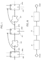
- Figure 1 of the annexed drawings shows by way of example a scan path comprising a plurality of flip-flops 100, 102, 104, ... (these flip-flops may be present in any rated number).
- Flip-flop 100 is assumed to be the first flip-flop in the scan path, while flip-flop 104 is considered to be ideally the last flip-flop.
- Logic blocks 120 are interposed between the individual flip-flops; they are assumed to be interposed between the output Q of the flip-flop upstream and the input D of the flip-flop downstream.
- the SI input of the individual flip-flop is connected to the output of the flip-flop upstream.
- the SI input of flip-flop 102 is connected to output Q, denoted by 100b, of flip-flop 100
- the SI input of flip-flop 104 is connected to output Q, denoted by 102b, of flip-flop 102.
- a scan path of the depicted kind generally comprises a much higher number of mutually cooperating flip-flops.
- shift mode and capture mode In particular, in order to perform the scan testing, it is possible to operate according to two different methods, which are known as shift mode and capture mode.
- the scan enable contact point acts as an interface for the automatic test unit, and allows the test unit to deliver a signal adapted to set the flip-flop into a shift mode.
- the flip-flops process the input signals received on input D, as it happens in the normal operating mode.
- a low level signal is applied on the SE input of the flip-flop.
- the number of internal clocks of an integrated circuit has an impact on the number of external pins.
- clock domains which phrase indicates a set of flip-flops and logic circuits that use the same clock. This fact may cause further difficulties in relation to a possible use of a common gate or a common flip-flop.
- independent clock domains i.e. clock domains that do not interfere with one another in any way, in a situation wherein the internal clocks supporting them may have different operating frequencies, which fact involves having for each clock domain a respective external pin supporting the testing function. This is a further difficulty as regards the soaring number of test pins.
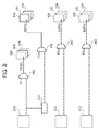
- FIG. 2 depicts a typical situation where the need exists to handle several internal clocks with different frequencies. These frequencies may correspond, for example, to the operating frequencies of various clock generators, denoted by CK1, CK1', CK2, CK3, etc.
- generator CK1 may be, for example, a PLL operating at an exemplary frequency of 72 MHz, with an associated divisor by two, which practically acts as a further clock generator CK1' operating at a frequency of 36 MHz, corresponding to half the frequency generated by generator CK1.
- generator CK2 can be an oscillator of any kind, operating for example at a frequency of 25 MHz
- clock generator CK3 may be an oscillating circuit RC, operating at a frequency of 16 MHz.
- the reported frequency values obviously have an exemplary value, and the choice of their respective value aims at highlighting that such clock signals and the related clock domains may operate at any frequency, without imposing or assuming any dependence constraint of such frequencies.
- Figure 2 refers mainly to the normal operating mode (without testing) of the device, and highlights the fact that the various clock domains, if necessary, can be "turned off” through clock gating cells 200, integrated in the circuit that must undergo testing.
- Cells 200 are subjected to control or enable (EN) signals and can comprise e.g. AND gates with two inputs, which respectively receive:
- the clock domain is active, and therefore the clock signal is supplied to flip-flops 100, 102, 104, ...; if the EN signal is at level "0", the clock domain is off.
- control or enable signal EN is to be distinguished from the scan enable signal SE.
- the solution in Figure 3 involves the use of plural pins, one for each test clock tst_ck1, tst_ck2, tst_ck3, tst_ck4, in order to solve the set up / hold issue among the various clock domains.
- a multiplexer 202 Upstream each cell 200, on the input that must receive the clock signal CK1, CK1', CK2, CK3, a multiplexer 202 is arranged which operates under the control of a test_mode signal.
- multiplexers 202 send, in place of the signal CK1, CK1', CK2, CK3, a corresponding signal tst_ck1, tst_ck2, tst_ck3, tst_ck4 to the cells 200.
- the firm Synopsis, Mountain View, California, USA offers a software tool that can be used in a design environment for integrated circuits and that is known as DFT_COMPILER.
- DFT_COMPILER Such a tool includes an application named OCC (On-Chip Clocking) that is adapted to manage various internal clocks of a circuit during a test operation.
- OCC On-Chip Clocking
- the inventors have moreover observed that also the previously mentioned tool, which can handle various internal clocks of a circuit during a testing operation, shows various disadvantages, for example a negative impact on the synthesis of so-called clock trees, and makes the circuit heavier in terms of area overhead.
- the object of the invention is to avoid the previously discussed drawbacks.
- the presently described solution allows the use of a single external pin, a feature that is particularly advantageous in the case of an "at speed scan test", being able to use a flip-flop which handles any clock domain.
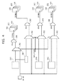
- FIG. 5 various embodiments can be considered as a development of the solution shown in Figure 4 .
- Such embodiments involve therefore the use of a single pin, common to all clock domains, on which a test signal test_clk is present, while upstream each cell 200, on the input that must receive the clock signal CK1, CK1', CK2, CK3, a multiplexer 202 is arranged which operates under the control of a test_mode signal.
- test_mode signal indicates that the circuit is being tested, multiplexers 202 send, in place of the signal CK1, CK1', CK2, CK3, a tst_clk signal to the cells 200.
- the clock gating cells 200 are provided, always referring for simplicity to an implementation with an AND gate, with a further input adapted to allow the performance of a clock gating function (particularly on the tst_clk signal, sent to the cells 200 from multiplexers 202 when the test_mode signal indicates the test mode).
- the said further input refers to a circuit 300 which includes (see Figures 6 and 7 ) a dedicated flip-flop 1000, itself integrated in circuit being tested.
- Flip-flop 1000 is adapted to perform a clock gating function at the desired frequency (for example, referring to the previously described values, and in no way by limitation, 72 MHz, 36 MHz, 25 MHz and 16 MHz).
- each flip-flop 1000 is supplied to the corresponding cell 200 through an OR gate 1002, interposed between flip-flop 1000 and cell 200 and having:
- Flip-flop 1000 receives the tst_clk signal as input.
- the respective inputs TI and TE on the contrary receive the scan in (SI) and scan enable (SE) signals, which have been described with reference to Figure 1 .
- the input D of flip-flop 1000 receives as a feedback the output of gate 1002, so as to avoid possible timing problems.
- the flow diagram in Figure 4 shows an operating mode whereby, after a START step, in a first shift step (SHIFT-IN) 50 the flip-flops are loaded to a known value.
- SHIFT-IN first shift step
- This step 50 is therefore named shift (in), and it lasts as many clock strikes as the length of the longest scan chain, in order to be able to load all flip-flops to the suitable value.
- This step 54 is perfectly equivalent to step 50, and in various embodiments steps 50 and 54 take place at the same time, because the shift-in of the new data to be loaded implies the simultaneous shift-out of the captured data.
- SHIFT and CAPTURE are two subsequent scan steps, that are discriminated by the SE value.
- step 54 moreover, the actually captured value is compared with the expected one, and during production all those elements showing differences are discarded.
- Various embodiments therefore allow to increase the parallelism in the system, because only one clock pin is needed to receive a clock signal from the outside, because the selective gating function of the clock is handled within the integrated circuit (through the flip-flops 1000).
- the area overhead is not excessive, as the overall addition only consists one single flip-flop and a gate, such as OR gate 1002, for each clock domain, which has a positive effect on the consumption, too.
Landscapes
- Engineering & Computer Science (AREA)
- General Engineering & Computer Science (AREA)
- Physics & Mathematics (AREA)
- General Physics & Mathematics (AREA)
- Semiconductor Integrated Circuits (AREA)
- Tests Of Electronic Circuits (AREA)
Abstract
A system for testing an integrated circuit including components (100, 102, 104), for receiving clock signals (CK1, CK1', CK2, CK3) corresponding to different clock domains, includes:
- a pin of the integrated circuit adapted to receive a test clock signal (tst_ck) for components (100, 102, 104) included in different clock domains,
- clock gating cells (200) integrated in the integrated circuit, to direct said test clock signal (tst_ck) from said pin towards components (100, 102, 104) included in respective clock domains, and
- coupled to each of the gating cells (200), a dedicated flip-flop (100) for a respective clock domain, said dedicated flip-flop being also integrated in the integrated circuit, to effect on the cell (200) to which it is coupled a clock gating function during test (50, 52, 54) of the integrated circuit.
- a pin of the integrated circuit adapted to receive a test clock signal (tst_ck) for components (100, 102, 104) included in different clock domains,
- clock gating cells (200) integrated in the integrated circuit, to direct said test clock signal (tst_ck) from said pin towards components (100, 102, 104) included in respective clock domains, and
- coupled to each of the gating cells (200), a dedicated flip-flop (100) for a respective clock domain, said dedicated flip-flop being also integrated in the integrated circuit, to effect on the cell (200) to which it is coupled a clock gating function during test (50, 52, 54) of the integrated circuit.
Description
- This disclosure relates to techniques for testing integrated circuits.
- This disclosure was devised with specific attention paid to its possible application to tests performed according to the methods known as "shift mode" and "capture mode". Such test modes are currently employed in the integrated circuit industry, particularly for consumer electronics.
- In the manufacture of integrated circuits, particularly of highly complex integrated circuits, the need arises to perform test operations on the components which constitute the circuit.
- Specifically, test techniques are known such as "scan testing", wherein, instead of performing a functional test at the integrated circuit level, tests are performed aiming at verifying the structure correctness.
- In an integrated circuit there may be provided as many as a million flip-flops and more, and the most widespread methods consider the circuit as a group of interconnected functional blocks. This makes it possible for example to design components such as the flip-flops included in a single functional block, in such a way as to allow them to be connected with one another in a so-called scan path, in order to undergo testing. Beside the inputs and outputs employed during a normal operation of the circuit, the flip-flops included in such a scan path include therefore additional terminals or pins, such as the ones named Scan Input (SI) and Scan Enable input (SE). The flip-flops included in a scan path are connected with their outputs to the SI input of the following flip-flop. The first flip-flop in the path receives an input stimulus from an automatic test unit, through an access terminal to the chip of the integrated circuit. The last flip-flop in the scan path gives in turn its output to the automatic test unit through a corresponding test access terminal. Within a single integrated circuit there may be several scan paths.
-
Figure 1 of the annexed drawings shows by way of example a scan path comprising a plurality of flip-flops flop 100 is assumed to be the first flip-flop in the scan path, while flip-flop 104 is considered to be ideally the last flip-flop.Logic blocks 120 are interposed between the individual flip-flops; they are assumed to be interposed between the output Q of the flip-flop upstream and the input D of the flip-flop downstream. - In
Figure 1 there are shown the previously mentioned SI and SE inputs, which are assumed to be ideally connected: - the SI (Scan Input) input to a scan input contact point, and
- the SE (Scan Enable) input to a scan enable contact point.
- For the subsequent flip-flops (e.g. flip-
flops 102 and 104), while keeping the connection of the SE input to the scan enable contact point, the SI input of the individual flip-flop is connected to the output of the flip-flop upstream. For instance, in the shown example, the SI input of flip-flop 102 is connected to output Q, denoted by 100b, of flip-flop 100, while the SI input of flip-flop 104 is connected to output Q, denoted by 102b, of flip-flop 102. - In this respect, it is to be remarked once again that the view in
Figure 1 is deliberately schematic in its essential elements: a scan path of the depicted kind generally comprises a much higher number of mutually cooperating flip-flops. - In particular, in order to perform the scan testing, it is possible to operate according to two different methods, which are known as shift mode and capture mode.
- In the shift mode, flip-flops process what they receive at their SI input. The scan enable contact point acts as an interface for the automatic test unit, and allows the test unit to deliver a signal adapted to set the flip-flop into a shift mode.
- In the capture mode, the flip-flops process the input signals received on input D, as it happens in the normal operating mode. In various embodiments, in order to shift to the capture mode a low level signal is applied on the SE input of the flip-flop.
- What has been said substantially corresponds to operating information and modes which are known in the state of the art, as reported for example in
US-A-2006/0075297 (US―B―7 500 165 ). - This document acknowledges the fact that the described techniques require the dedication of external pins of the integrated circuit to the scan testing function, in order to allow the connection to the automatic test devices.
- Although use is not made of a plurality of external pins dedicated to the test, by resorting to the functional pins being shared and having a specific meaning in test mode, in any case the need is felt to limit the number of external pins used; this is due to various different reasons:
- a low functional pin count is available,
- the necessary hardware for the test should be reduced (channels of the testing device),
- with the same number of channels, parallelism (the number of simultaneously tested devices) should be increased, and
- generally speaking, it is desirable to minimize the number of external pins dedicated to testing, so as to reduce dimensions and/or to dedicate a higher number of pins to the circuit functions.
- Moreover, the number of internal clocks of an integrated circuit has an impact on the number of external pins. In a currently employed chip there may be as many as hundreds of different "clock domains", which phrase indicates a set of flip-flops and logic circuits that use the same clock. This fact may cause further difficulties in relation to a possible use of a common gate or a common flip-flop. Actually, there may exist independent clock domains, i.e. clock domains that do not interfere with one another in any way, in a situation wherein the internal clocks supporting them may have different operating frequencies, which fact involves having for each clock domain a respective external pin supporting the testing function. This is a further difficulty as regards the soaring number of test pins.
- Specifically, the diagram in
Figure 2 depicts a typical situation where the need exists to handle several internal clocks with different frequencies. These frequencies may correspond, for example, to the operating frequencies of various clock generators, denoted by CK1, CK1', CK2, CK3, etc. - By way of example and not of limitation of the scope of the present disclosure, generator CK1 may be, for example, a PLL operating at an exemplary frequency of 72 MHz, with an associated divisor by two, which practically acts as a further clock generator CK1' operating at a frequency of 36 MHz, corresponding to half the frequency generated by generator CK1. Similarly, generator CK2 can be an oscillator of any kind, operating for example at a frequency of 25 MHz, while clock generator CK3 may be an oscillating circuit RC, operating at a frequency of 16 MHz. The reported frequency values obviously have an exemplary value, and the choice of their respective value aims at highlighting that such clock signals and the related clock domains may operate at any frequency, without imposing or assuming any dependence constraint of such frequencies.
-
Figure 2 refers mainly to the normal operating mode (without testing) of the device, and highlights the fact that the various clock domains, if necessary, can be "turned off" throughclock gating cells 200, integrated in the circuit that must undergo testing. -
Cells 200 are subjected to control or enable (EN) signals and can comprise e.g. AND gates with two inputs, which respectively receive: - on one input, the clock signal CK1, CK1', CK2, CK3, and
- on the other input, the EN signal.
- As a consequence, if the EN signal is at level "1", the clock domain is active, and therefore the clock signal is supplied to flip-
flops - For the sake of clarity it should be noted that, in the solution considered in
Figure 2 , the control or enable signal EN is to be distinguished from the scan enable signal SE. - In order to test the circuit, the structure depicted in
Figure 2 is adapted to be implemented, according to conventional solutions, with two different approaches, that are respectively illustrated inFigure 3 and inFigure 4 . In these two Figures, parts and components identical or equivalent to parts and components already described with reference toFigures 1 and2 are denoted by the same reference numbers, and the description thereof will be omitted. - Specifically, the solution in
Figure 3 involves the use of plural pins, one for each test clock tst_ck1, tst_ck2, tst_ck3, tst_ck4, in order to solve the set up / hold issue among the various clock domains. Upstream eachcell 200, on the input that must receive the clock signal CK1, CK1', CK2, CK3, amultiplexer 202 is arranged which operates under the control of a test_mode signal. When the test_mode signal shows that the circuit is being tested,multiplexers 202 send, in place of the signal CK1, CK1', CK2, CK3, a corresponding signal tst_ck1, tst_ck2, tst_ck3, tst_ck4 to thecells 200. - The solution in
Figure 4 involves on the contrary the use of a single pin, common to all clock domains, on which a test clock signal tst_ck is present. In this case as well, upstream eachcell 200, on the input that must receive the clock signal CK1, CK1', CK2, CK3, amultiplexer 202 is arranged which operates under the control of a test_mode signal. When the test_mode signal indicates that the circuit is being tested,multiplexers 202 send, in place of the signal CK1, CK1', CK2, CK3, a signal tst_clk to thecells 200. In this case the need arises to handle timing issues among the different clock signals. - The firm Synopsis, Mountain View, California, USA offers a software tool that can be used in a design environment for integrated circuits and that is known as DFT_COMPILER. Such a tool includes an application named OCC (On-Chip Clocking) that is adapted to manage various internal clocks of a circuit during a test operation.
- The inventors have observed that the solution previously considered with reference to
Figures 2 and4 suffers from some major drawbacks. - Specifically, in the case that one pin for each clock domain is employed, the number of necessary pads to handle a corresponding number of different clock domains increases, which fact results in a lower ability to operate in parallelism.
- If a common pin is used for all clock domains, a problem arises concerning the clock rate of the different clock domains, with the addition of the fact that a rather long processing time is required in order to generate the corresponding test patterns.
- The inventors have moreover observed that also the previously mentioned tool, which can handle various internal clocks of a circuit during a testing operation, shows various disadvantages, for example a negative impact on the synthesis of so-called clock trees, and makes the circuit heavier in terms of area overhead.
- The object of the invention is to avoid the previously discussed drawbacks.
- According to the present invention, such an object is achieved thanks to a system having the features set forth in the claims that follow.
- The claims are an integral part of the technical teaching of the invention provided herein.
- In various embodiments, the presently described solution allows the use of a single external pin, a feature that is particularly advantageous in the case of an "at speed scan test", being able to use a flip-flop which handles any clock domain.
- The invention will now be described, by way of example only, with reference to the enclosed representations, wherein:
-
Figures 1 to 4 have been previously described, -
Figure 5 shows an exemplary embodiment; -
Figures 6 and 7 show two possible embodiment solutions, and -
Figure 8 is a flow diagram showing the ways in which the embodiments can be employed. - In the following description, numerous specific details are given to provide a thorough understanding of embodiments. The embodiments can be practiced without one or more of the specific details, or with other methods, components, materials, etc. In other instances, well-known structures, materials, or operations are not shown or described in detail to avoid obscuring aspects of the embodiments.
- Reference throughout this specification to "one embodiment" or "an embodiment" means that a particular feature, structure, or characteristic described in connection with the embodiment is included in at least one embodiment. Thus, the appearances of the phrases "in one embodiment" or "in an embodiment" in various places throughout this specification are not necessarily all referring to the same embodiment. Furthermore, the particular features, structures, or characteristics may be combined in any suitable manner in one or more embodiments.
- The headings provided herein are for convenience only and do not interpret the scope or meaning of the embodiments.
- In
Figure 5 and in the subsequent Figures, parts and components identical or equivalent to parts and components already described with reference toFigures 1 and4 are denoted by the same reference numbers, and the description thereof will be omitted. - As exemplified in
Figure 5 , various embodiments can be considered as a development of the solution shown inFigure 4 . Such embodiments involve therefore the use of a single pin, common to all clock domains, on which a test signal test_clk is present, while upstream eachcell 200, on the input that must receive the clock signal CK1, CK1', CK2, CK3, amultiplexer 202 is arranged which operates under the control of a test_mode signal. When the test_mode signal indicates that the circuit is being tested,multiplexers 202 send, in place of the signal CK1, CK1', CK2, CK3, a tst_clk signal to thecells 200. - In
Figure 5 , theclock gating cells 200 are provided, always referring for simplicity to an implementation with an AND gate, with a further input adapted to allow the performance of a clock gating function (particularly on the tst_clk signal, sent to thecells 200 frommultiplexers 202 when the test_mode signal indicates the test mode). - In various embodiments, the said further input refers to a
circuit 300 which includes (seeFigures 6 and 7 ) a dedicated flip-flop 1000, itself integrated in circuit being tested. - Flip-
flop 1000 is adapted to perform a clock gating function at the desired frequency (for example, referring to the previously described values, and in no way by limitation, 72 MHz, 36 MHz, 25 MHz and 16 MHz). - In this way it is possible to control various clocks from a single pin, so as to perform, for example, a function of selecting a clock gating during the capture step, so as to perform an "at speed test" without encountering timing problems.
- In various embodiments, depicted in particular in
Figures 6 and 7 , the signal coming from each flip-flop 1000 is supplied to thecorresponding cell 200 through anOR gate 1002, interposed between flip-flop 1000 andcell 200 and having: - as a first input, the output signal from flip-
flop 1000, and - as a second input, the scan enable signal SE which has already been discussed in the introductory section of the present disclosure.
- Flip-
flop 1000 receives the tst_clk signal as input. The respective inputs TI and TE on the contrary receive the scan in (SI) and scan enable (SE) signals, which have been described with reference toFigure 1 . The input D of flip-flop 1000 receives as a feedback the output ofgate 1002, so as to avoid possible timing problems. - The two embodiments of
Figures 6 and 7 differ in the following features: - in the embodiment of
Figure 6 (mask system active low) the output signal of flip-flop 1000 is supplied to the input of theOR gate 1002 in a direct form; - in the embodiment of
Figure 7 (mask system active high) the output signal of flip-flop 1000 is supplied to the input of theOR gate 1002 in negated form (i.e. with inverted logic). - The output of
gate 1002, connected with an input ofcell 200, transfers tocell 100 the signal of flip-flop 1000 subjected to gating by the signal SE. - In this way it is possible to have a dedicated flip-
flop 1000 for each clock domain / frequency, and to handle the generation of patterns in a flexible way, by using the flip-flop 1000 (which is in turn adapted to be tested with the scan technique). - Specifically, the flow diagram in
Figure 4 shows an operating mode whereby, after a START step, in a first shift step (SHIFT-IN) 50 the flip-flops are loaded to a known value. In order to achieve this, all shift chains are carried out, i.e. all flip-flops step 50 is therefore named shift (in), and it lasts as many clock strikes as the length of the longest scan chain, in order to be able to load all flip-flops to the suitable value. - Once the device has been configured, the signal SE is brought to the value SE=0 (capture), in order to be able to select, in
step 52, the input D of the flip-flops, i.e. the functional input. - Subsequently, in a second shift step (SHIFT-OUT) 54, the signal is brought back to the value SE=1, in order to reconfigure the scan chains so as to observe the capture value serially. This
step 54 is perfectly equivalent to step 50, and in various embodiments steps 50 and 54 take place at the same time, because the shift-in of the new data to be loaded implies the simultaneous shift-out of the captured data. - In practice, SHIFT and CAPTURE are two subsequent scan steps, that are discriminated by the SE value.
- In
step 54, moreover, the actually captured value is compared with the expected one, and during production all those elements showing differences are discarded. - The general criteria for the execution of a test of the presently described type are anyway generally known, and therefore do not require a more detailed description herein.
- Various embodiments therefore allow to increase the parallelism in the system, because only one clock pin is needed to receive a clock signal from the outside, because the selective gating function of the clock is handled within the integrated circuit (through the flip-flops 1000).
- The area overhead is not excessive, as the overall addition only consists one single flip-flop and a gate, such as
OR gate 1002, for each clock domain, which has a positive effect on the consumption, too. - Various embodiments have a negligible impact on the function of clock tree synthesis, as it is also possible to execute tests on inter-clock domains.
- All these features are embodied in a solution of simple implementation, with the further advantage of time saving in the development flow as compared to the solution involving a test clock for each clock domain.
- Of course, without prejudice to the underlying principles of the invention, the details and the embodiments may vary, even appreciably, with respect to what has been described by way of example only, without departing from the scope of the invention as defined by the claims that follow.
Claims (8)
- A system for testing an integrated circuit including components (100, 102, 104) for receiving clock signals (CK1, CK1', CK2, CK3) corresponding to different clock domains, the system including:- a pin of the integrated circuit to receive a test clock signal (tst_ck) for components (100, 102, 104) included in different clock domains,- clock gating cells (200) integrated in the integrated circuit to direct said test clock signal (tst_ck) from said pin towards components (100, 102, 104) included in respective clock domains, and- coupled to each of said gating cells (200), a dedicated flip-flop (1000) for a respective clock domain, said dedicated flip-flop being also integrated in the integrated circuit to effect on the cell (200) to which it is coupled a clock gating function during test (50, 52, 54) of the integrated circuit.
- The system of claim 1, including multiplexers (202) controlled by a signal (test_mode) indicative of a test phase, to send toward said clock gating cells (200), in said test phase, said test clock signal (tst_ck) in the place of one of said clock signals (CK1, CK1', CK2, CK3).
- The system of claim 1 or claim 2, including a logic gate (1002) interposed between said dedicated flip-flop (1000) and said clock gating cell (200) coupled thereto to effect a gating function based on a scan enable signal (SE) by correspondingly managing generation of test patterns for the circuit.
- The system of claim 3, wherein the output of said logic gate (1002) is feedback connected to the input, preferably to the D input, of said dedicated flip-flop (1000).
- The system of claim 3 or claim 4, wherein said logic gate (1002) is an OR gate receiving said scan enable signal (SE) on an input and the output signal of said dedicated flip-flop (1000) on another input.
- The system of any of claims 3 to 5, wherein said logic gate (1002) receives the output signal of said dedicated flip-flop (1000) in direct form.
- The system of any of claims 3 to 5, wherein said logic gate (1002) receives the output signal of said dedicated flip-flop (1000) in negated form.
- The system of any of the claims 1 to 7 wherein said gating cells (200) are AND gates.
Applications Claiming Priority (1)
| Application Number | Priority Date | Filing Date | Title |
|---|---|---|---|
| ITTO20100268 | 2010-04-08 |
Publications (1)
| Publication Number | Publication Date |
|---|---|
| EP2378425A1 true EP2378425A1 (en) | 2011-10-19 |
Family
ID=43071446
Family Applications (1)
| Application Number | Title | Priority Date | Filing Date |
|---|---|---|---|
| EP11160477A Withdrawn EP2378425A1 (en) | 2010-04-08 | 2011-03-30 | A testing system for integrated circuits |
Country Status (2)
| Country | Link |
|---|---|
| US (1) | US8788895B2 (en) |
| EP (1) | EP2378425A1 (en) |
Families Citing this family (5)
| Publication number | Priority date | Publication date | Assignee | Title |
|---|---|---|---|---|
| US8656326B1 (en) | 2013-02-13 | 2014-02-18 | Atrenta, Inc. | Sequential clock gating using net activity and XOR technique on semiconductor designs including already gated pipeline design |
| US10775435B1 (en) * | 2018-11-01 | 2020-09-15 | Cadence Design Systems, Inc. | Low-power shift with clock staggering |
| TWI730707B (en) * | 2020-04-01 | 2021-06-11 | 瑞昱半導體股份有限公司 | Clock gating cell |
| CN113497606B (en) * | 2020-04-08 | 2024-02-23 | 瑞昱半导体股份有限公司 | Clock gating unit |
| WO2025264207A1 (en) * | 2024-06-17 | 2025-12-26 | Google Llc | Enhancing test-control connectivity for clock gating |
Citations (5)
| Publication number | Priority date | Publication date | Assignee | Title |
|---|---|---|---|---|
| US6715093B1 (en) * | 2000-04-28 | 2004-03-30 | Hewlett-Packard Development Company, L.P. | Method for triggering an asynchronous event by creating a lowest common denominator clock |
| US20050022083A1 (en) * | 2003-07-02 | 2005-01-27 | Chi-Feng Wu | System and method for performing scan test with single scan clock |
| US20050055614A1 (en) * | 2003-09-10 | 2005-03-10 | Ta-Chia Yeh | Multi-clock domain logic system and related method |
| US20060075297A1 (en) | 2004-10-06 | 2006-04-06 | Broadcom Corporation | Systems and methods for controlling clock signals during scan testing integrated circuits |
| US20080282122A1 (en) * | 2007-05-09 | 2008-11-13 | Amar Guettaf | Single scan clock in a multi-clock domain |
Family Cites Families (7)
| Publication number | Priority date | Publication date | Assignee | Title |
|---|---|---|---|---|
| US7552360B2 (en) * | 2005-03-21 | 2009-06-23 | Texas Instruments Incorporated | Debug and test system with format select register circuitry |
| US8145958B2 (en) * | 2005-11-10 | 2012-03-27 | Arm Limited | Integrated circuit and method for testing memory on the integrated circuit |
| TW200801550A (en) * | 2006-01-06 | 2008-01-01 | Koninkl Philips Electronics Nv | IC testing methods and apparatus |
| US7640475B2 (en) * | 2006-03-30 | 2009-12-29 | Texas Instruments Incorporated | At-speed transition fault testing with low speed scan enable |
| DE102006024507B4 (en) * | 2006-05-23 | 2017-06-01 | Infineon Technologies Ag | Integrated circuit and method for detecting runtime errors in integrated circuits |
| JP5275136B2 (en) * | 2009-05-28 | 2013-08-28 | ルネサスエレクトロニクス株式会社 | Semiconductor integrated circuit |
| US8464117B2 (en) * | 2010-05-25 | 2013-06-11 | Freescale Semiconductor, Inc. | System for testing integrated circuit with asynchronous clock domains |
-
2011
- 2011-03-17 US US13/050,611 patent/US8788895B2/en active Active
- 2011-03-30 EP EP11160477A patent/EP2378425A1/en not_active Withdrawn
Patent Citations (6)
| Publication number | Priority date | Publication date | Assignee | Title |
|---|---|---|---|---|
| US6715093B1 (en) * | 2000-04-28 | 2004-03-30 | Hewlett-Packard Development Company, L.P. | Method for triggering an asynchronous event by creating a lowest common denominator clock |
| US20050022083A1 (en) * | 2003-07-02 | 2005-01-27 | Chi-Feng Wu | System and method for performing scan test with single scan clock |
| US20050055614A1 (en) * | 2003-09-10 | 2005-03-10 | Ta-Chia Yeh | Multi-clock domain logic system and related method |
| US20060075297A1 (en) | 2004-10-06 | 2006-04-06 | Broadcom Corporation | Systems and methods for controlling clock signals during scan testing integrated circuits |
| US7500165B2 (en) | 2004-10-06 | 2009-03-03 | Broadcom Corporation | Systems and methods for controlling clock signals during scan testing integrated circuits |
| US20080282122A1 (en) * | 2007-05-09 | 2008-11-13 | Amar Guettaf | Single scan clock in a multi-clock domain |
Also Published As
| Publication number | Publication date |
|---|---|
| US8788895B2 (en) | 2014-07-22 |
| US20110248720A1 (en) | 2011-10-13 |
Similar Documents
| Publication | Publication Date | Title |
|---|---|---|
| JP3291350B2 (en) | Equipment for testing digital systems | |
| US8904255B2 (en) | Integrated circuit having clock gating circuitry responsive to scan shift control signal | |
| CN100587508C (en) | Scan chain and method for realizing high-speed test circuit | |
| US20140101500A1 (en) | Circuits and methods for functional testing of integrated circuit chips | |
| US7038494B2 (en) | Scan chain element and associated method | |
| US7124340B2 (en) | Low pin count, high-speed boundary scan testing | |
| CN110007217B (en) | A Low Power Consumption Boundary Scan Test Method | |
| CN111624478B (en) | A clock signal control circuit and device | |
| CN110346618A (en) | A kind of OCC circuit being directed to multi-clock zone at-speed test | |
| CN114280454A (en) | Chip testing method and device, chip testing machine and storage medium | |
| US8898527B2 (en) | At-speed scan testing of clock divider logic in a clock module of an integrated circuit | |
| US20110296265A1 (en) | System for testing integrated circuit with asynchronous clock domains | |
| US20160349318A1 (en) | Dynamic Clock Chain Bypass | |
| US8850280B2 (en) | Scan enable timing control for testing of scan cells | |
| US20090187801A1 (en) | Method and system to perform at-speed testing | |
| US8788895B2 (en) | Testing system for integrated circuits including components for receiving clock signals corresponding to different clock domains | |
| US20080282122A1 (en) | Single scan clock in a multi-clock domain | |
| KR100870037B1 (en) | Easy to test semiconductor device, test method of semiconductor device, test clock generation method and device for semiconductor device test | |
| CN118465523A (en) | A high-speed scan test method for asynchronous clock domain integrated circuits | |
| US9891279B2 (en) | Managing IR drop | |
| US7870452B2 (en) | Scan testing methods | |
| US8832510B2 (en) | Circuit to reduce peak power during transition fault testing of integrated circuit | |
| US20140201584A1 (en) | Scan test circuitry comprising at least one scan chain and associated reset multiplexing circuitry | |
| US8302065B2 (en) | Device and method for testing a device | |
| JP4356942B2 (en) | Integrated circuit and test method thereof |
Legal Events
| Date | Code | Title | Description |
|---|---|---|---|
| AK | Designated contracting states |
Kind code of ref document: A1 Designated state(s): AL AT BE BG CH CY CZ DE DK EE ES FI FR GB GR HR HU IE IS IT LI LT LU LV MC MK MT NL NO PL PT RO RS SE SI SK SM TR |
|
| AX | Request for extension of the european patent |
Extension state: BA ME |
|
| PUAI | Public reference made under article 153(3) epc to a published international application that has entered the european phase |
Free format text: ORIGINAL CODE: 0009012 |
|
| RAP1 | Party data changed (applicant data changed or rights of an application transferred) |
Owner name: STMICROELECTRONICS (ROUSSET) SAS Owner name: STMICROELECTRONICS SRL |
|
| STAA | Information on the status of an ep patent application or granted ep patent |
Free format text: STATUS: THE APPLICATION IS DEEMED TO BE WITHDRAWN |
|
| 18D | Application deemed to be withdrawn |
Effective date: 20120420 |