EP2378327A2 - Light guide panel assembly - Google Patents
Light guide panel assembly Download PDFInfo
- Publication number
- EP2378327A2 EP2378327A2 EP20110162511 EP11162511A EP2378327A2 EP 2378327 A2 EP2378327 A2 EP 2378327A2 EP 20110162511 EP20110162511 EP 20110162511 EP 11162511 A EP11162511 A EP 11162511A EP 2378327 A2 EP2378327 A2 EP 2378327A2
- Authority
- EP
- European Patent Office
- Prior art keywords
- panel
- light
- light guide
- rear face
- assembly
- Prior art date
- Legal status (The legal status is an assumption and is not a legal conclusion. Google has not performed a legal analysis and makes no representation as to the accuracy of the status listed.)
- Granted
Links
Images




Classifications
-
- B—PERFORMING OPERATIONS; TRANSPORTING
- B21—MECHANICAL METAL-WORKING WITHOUT ESSENTIALLY REMOVING MATERIAL; PUNCHING METAL
- B21C—MANUFACTURE OF METAL SHEETS, WIRE, RODS, TUBES, PROFILES OR LIKE SEMI-MANUFACTURED PRODUCTS OTHERWISE THAN BY ROLLING; AUXILIARY OPERATIONS USED IN CONNECTION WITH METAL-WORKING WITHOUT ESSENTIALLY REMOVING MATERIAL
- B21C37/00—Manufacture of metal sheets, rods, wire, tubes, profiles or like semi-manufactured products, not otherwise provided for; Manufacture of tubes of special shape
- B21C37/06—Manufacture of metal sheets, rods, wire, tubes, profiles or like semi-manufactured products, not otherwise provided for; Manufacture of tubes of special shape of tubes or metal hoses; Combined procedures for making tubes, e.g. for making multi-wall tubes
- B21C37/15—Making tubes of special shape; Making tube fittings
- B21C37/20—Making helical or similar guides in or on tubes without removing material, e.g. by drawing same over mandrels, by pushing same through dies ; Making tubes with angled walls, ribbed tubes or tubes with decorated walls
- B21C37/207—Making helical or similar guides in or on tubes without removing material, e.g. by drawing same over mandrels, by pushing same through dies ; Making tubes with angled walls, ribbed tubes or tubes with decorated walls with helical guides
-
- G—PHYSICS
- G02—OPTICS
- G02B—OPTICAL ELEMENTS, SYSTEMS OR APPARATUS
- G02B6/00—Light guides; Structural details of arrangements comprising light guides and other optical elements, e.g. couplings
- G02B6/24—Coupling light guides
- G02B6/42—Coupling light guides with opto-electronic elements
- G02B6/4201—Packages, e.g. shape, construction, internal or external details
-
- F—MECHANICAL ENGINEERING; LIGHTING; HEATING; WEAPONS; BLASTING
- F28—HEAT EXCHANGE IN GENERAL
- F28D—HEAT-EXCHANGE APPARATUS, NOT PROVIDED FOR IN ANOTHER SUBCLASS, IN WHICH THE HEAT-EXCHANGE MEDIA DO NOT COME INTO DIRECT CONTACT
- F28D15/00—Heat-exchange apparatus with the intermediate heat-transfer medium in closed tubes passing into or through the conduit walls ; Heat-exchange apparatus employing intermediate heat-transfer medium or bodies
- F28D15/02—Heat-exchange apparatus with the intermediate heat-transfer medium in closed tubes passing into or through the conduit walls ; Heat-exchange apparatus employing intermediate heat-transfer medium or bodies in which the medium condenses and evaporates, e.g. heat pipes
- F28D15/04—Heat-exchange apparatus with the intermediate heat-transfer medium in closed tubes passing into or through the conduit walls ; Heat-exchange apparatus employing intermediate heat-transfer medium or bodies in which the medium condenses and evaporates, e.g. heat pipes with tubes having a capillary structure
- F28D15/046—Heat-exchange apparatus with the intermediate heat-transfer medium in closed tubes passing into or through the conduit walls ; Heat-exchange apparatus employing intermediate heat-transfer medium or bodies in which the medium condenses and evaporates, e.g. heat pipes with tubes having a capillary structure characterised by the material or the construction of the capillary structure
-
- G—PHYSICS
- G02—OPTICS
- G02B—OPTICAL ELEMENTS, SYSTEMS OR APPARATUS
- G02B6/00—Light guides; Structural details of arrangements comprising light guides and other optical elements, e.g. couplings
- G02B6/0001—Light guides; Structural details of arrangements comprising light guides and other optical elements, e.g. couplings specially adapted for lighting devices or systems
- G02B6/0011—Light guides; Structural details of arrangements comprising light guides and other optical elements, e.g. couplings specially adapted for lighting devices or systems the light guides being planar or of plate-like form
- G02B6/0013—Means for improving the coupling-in of light from the light source into the light guide
- G02B6/0015—Means for improving the coupling-in of light from the light source into the light guide provided on the surface of the light guide or in the bulk of it
- G02B6/002—Means for improving the coupling-in of light from the light source into the light guide provided on the surface of the light guide or in the bulk of it by shaping at least a portion of the light guide, e.g. with collimating, focussing or diverging surfaces
- G02B6/0021—Means for improving the coupling-in of light from the light source into the light guide provided on the surface of the light guide or in the bulk of it by shaping at least a portion of the light guide, e.g. with collimating, focussing or diverging surfaces for housing at least a part of the light source, e.g. by forming holes or recesses
-
- G—PHYSICS
- G02—OPTICS
- G02B—OPTICAL ELEMENTS, SYSTEMS OR APPARATUS
- G02B6/00—Light guides; Structural details of arrangements comprising light guides and other optical elements, e.g. couplings
- G02B6/0001—Light guides; Structural details of arrangements comprising light guides and other optical elements, e.g. couplings specially adapted for lighting devices or systems
- G02B6/0011—Light guides; Structural details of arrangements comprising light guides and other optical elements, e.g. couplings specially adapted for lighting devices or systems the light guides being planar or of plate-like form
- G02B6/0033—Means for improving the coupling-out of light from the light guide
-
- G—PHYSICS
- G02—OPTICS
- G02B—OPTICAL ELEMENTS, SYSTEMS OR APPARATUS
- G02B6/00—Light guides; Structural details of arrangements comprising light guides and other optical elements, e.g. couplings
- G02B6/0001—Light guides; Structural details of arrangements comprising light guides and other optical elements, e.g. couplings specially adapted for lighting devices or systems
- G02B6/0011—Light guides; Structural details of arrangements comprising light guides and other optical elements, e.g. couplings specially adapted for lighting devices or systems the light guides being planar or of plate-like form
- G02B6/0033—Means for improving the coupling-out of light from the light guide
- G02B6/0058—Means for improving the coupling-out of light from the light guide varying in density, size, shape or depth along the light guide
- G02B6/0061—Means for improving the coupling-out of light from the light guide varying in density, size, shape or depth along the light guide to provide homogeneous light output intensity
-
- G—PHYSICS
- G02—OPTICS
- G02B—OPTICAL ELEMENTS, SYSTEMS OR APPARATUS
- G02B6/00—Light guides; Structural details of arrangements comprising light guides and other optical elements, e.g. couplings
- G02B6/0001—Light guides; Structural details of arrangements comprising light guides and other optical elements, e.g. couplings specially adapted for lighting devices or systems
- G02B6/0011—Light guides; Structural details of arrangements comprising light guides and other optical elements, e.g. couplings specially adapted for lighting devices or systems the light guides being planar or of plate-like form
- G02B6/0081—Mechanical or electrical aspects of the light guide and light source in the lighting device peculiar to the adaptation to planar light guides, e.g. concerning packaging
-
- G—PHYSICS
- G02—OPTICS
- G02B—OPTICAL ELEMENTS, SYSTEMS OR APPARATUS
- G02B6/00—Light guides; Structural details of arrangements comprising light guides and other optical elements, e.g. couplings
- G02B6/0001—Light guides; Structural details of arrangements comprising light guides and other optical elements, e.g. couplings specially adapted for lighting devices or systems
- G02B6/0011—Light guides; Structural details of arrangements comprising light guides and other optical elements, e.g. couplings specially adapted for lighting devices or systems the light guides being planar or of plate-like form
- G02B6/0081—Mechanical or electrical aspects of the light guide and light source in the lighting device peculiar to the adaptation to planar light guides, e.g. concerning packaging
- G02B6/0085—Means for removing heat created by the light source from the package
-
- G—PHYSICS
- G02—OPTICS
- G02B—OPTICAL ELEMENTS, SYSTEMS OR APPARATUS
- G02B6/00—Light guides; Structural details of arrangements comprising light guides and other optical elements, e.g. couplings
- G02B6/0001—Light guides; Structural details of arrangements comprising light guides and other optical elements, e.g. couplings specially adapted for lighting devices or systems
- G02B6/0011—Light guides; Structural details of arrangements comprising light guides and other optical elements, e.g. couplings specially adapted for lighting devices or systems the light guides being planar or of plate-like form
- G02B6/0033—Means for improving the coupling-out of light from the light guide
- G02B6/0035—Means for improving the coupling-out of light from the light guide provided on the surface of the light guide or in the bulk of it
- G02B6/0038—Linear indentations or grooves, e.g. arc-shaped grooves or meandering grooves, extending over the full length or width of the light guide
-
- G—PHYSICS
- G02—OPTICS
- G02B—OPTICAL ELEMENTS, SYSTEMS OR APPARATUS
- G02B6/00—Light guides; Structural details of arrangements comprising light guides and other optical elements, e.g. couplings
- G02B6/0001—Light guides; Structural details of arrangements comprising light guides and other optical elements, e.g. couplings specially adapted for lighting devices or systems
- G02B6/0011—Light guides; Structural details of arrangements comprising light guides and other optical elements, e.g. couplings specially adapted for lighting devices or systems the light guides being planar or of plate-like form
- G02B6/0066—Light guides; Structural details of arrangements comprising light guides and other optical elements, e.g. couplings specially adapted for lighting devices or systems the light guides being planar or of plate-like form characterised by the light source being coupled to the light guide
- G02B6/0068—Arrangements of plural sources, e.g. multi-colour light sources
-
- G—PHYSICS
- G02—OPTICS
- G02B—OPTICAL ELEMENTS, SYSTEMS OR APPARATUS
- G02B6/00—Light guides; Structural details of arrangements comprising light guides and other optical elements, e.g. couplings
- G02B6/0001—Light guides; Structural details of arrangements comprising light guides and other optical elements, e.g. couplings specially adapted for lighting devices or systems
- G02B6/0011—Light guides; Structural details of arrangements comprising light guides and other optical elements, e.g. couplings specially adapted for lighting devices or systems the light guides being planar or of plate-like form
- G02B6/0066—Light guides; Structural details of arrangements comprising light guides and other optical elements, e.g. couplings specially adapted for lighting devices or systems the light guides being planar or of plate-like form characterised by the light source being coupled to the light guide
- G02B6/0073—Light emitting diode [LED]
-
- G—PHYSICS
- G02—OPTICS
- G02B—OPTICAL ELEMENTS, SYSTEMS OR APPARATUS
- G02B6/00—Light guides; Structural details of arrangements comprising light guides and other optical elements, e.g. couplings
- G02B6/0001—Light guides; Structural details of arrangements comprising light guides and other optical elements, e.g. couplings specially adapted for lighting devices or systems
- G02B6/0011—Light guides; Structural details of arrangements comprising light guides and other optical elements, e.g. couplings specially adapted for lighting devices or systems the light guides being planar or of plate-like form
- G02B6/0081—Mechanical or electrical aspects of the light guide and light source in the lighting device peculiar to the adaptation to planar light guides, e.g. concerning packaging
- G02B6/0083—Details of electrical connections of light sources to drivers, circuit boards, or the like
Definitions
- This invention relates to light guide panel assemblies.
- Such panel assemblies can be used to provide illuminated signs, such as road signs, which may convey a message by virtue of their shape or by masking provided on the panel assembly. They may also be used for back-lighting of displays such as liquid crystal computer screens or television screens.
- a conventional panel assembly of this type comprises a translucent panel (for example of acrylic) and at least one light-emitting device (such as an light emitting diode, or LED) arranged for producing a divergent beam of light and projecting the light into the panel from a light-receiving edge of the panel.
- a translucent panel for example of acrylic
- at least one light-emitting device such as an light emitting diode, or LED
- the light passes through the panel, it is internally reflected by the front and rear faces of the panel and at least some of the light is transmitted by at least one light-emitting surface portion of at least one of the faces so as to illuminate that surface portion.
- At least one other surface portion of that face may be opaque so that an illuminated pattern is formed on that face.
- substantially all of one or each face may be light-emitting, so that the whole face (which may have a particular shape such as a direction arrow) is illuminated.
- the light-emitting face of the panel assembly provides uniform illumination (other than in areas where the face is intended to be masked).
- the further the light travels through the panel from the light-emitting device the less intense it becomes.
- the light-emitting device(s) are not properly positioned, for example being canted over, they can produce aberrations in the illumination.
- An aim of the present invention is to provide a light guide panel assembly which can: conduct heat effectively away from the light-emitting device(s); establish and maintain proper positioning of the light emitting device(s); provide a seal against ingress of moisture to the light-emitting devices; provide substantially uniform illumination of the light-emitting face of the panel assembly (other than in areas where the face is intended to be masked); and accomplish all of the aforesaid in a simple, convenient and inexpensive manner.
- a light guide panel assembly comprising: a translucent panel; a light-emitting device (such as an LED) arranged for producing a divergent beam of light and projecting the light into the panel from a light-receiving edge of the panel; a heatsink; and a compressible, thermally-conductive element disposed in compression against the heatsink and so as to urge the light-emitting device against the light-receiving edge of the panel and to provide a thermal pathway between the light-emitting device and the heatsink.
- the compressible element therefore serves the dual purposes of holding the light-emitting device in place and also assisting in conducting heat away from it. In some embodiments, it can also serve as a seal to prevent ingress of moisture to the light-emitting device.
- the light emitting device is preferably one of a plurality of such light-emitting devices mounted on one face of a common, elongate circuit board, and the compressible element is preferably elongate and is compressed against the heatsink and an opposite face of the circuit board.
- the light-receiving edge of the panel may include at least a portion which is not straight, in which case the circuit board is preferably flexible and conforms to the shape of the light-receiving edge of the panel. This conveniently enables complex shapes of panel assembly to be provided.
- the circuit board may have connection pads at each end of the circuit board, so that a plurality of the circuit boards can be daisy-chained together in a single panel assembly and/or in separate panel assemblies.
- the light-receiving edge of the panel is preferably formed by a side wall of a groove formed in one face of the panel, the light-emitting device(s) and compressible element being disposed in the groove, therefore enabling the opposite face of the panel to be uninterrupted.
- the compressible element is preferably disposed in compression against a bottom wall of the groove and against an opposite side wall of the groove, with the heatsink closing off the groove at the rear face of the panel.
- a front face of the panel preferably has at least one light-emitting surface portion which specularly reflects and transmits light incident thereon from within the panel, and a rear face of the panel preferably specularly reflects and scatteringly reflects light incident thereon from within the panel. This enables the panel to act as a light guide and to illuminate the front face.
- the rear face of the panel preferably specularly reflects and scatteringly reflects light incident thereon from within the panel with a ratio of specular to scattering reflection which is non-uniform across the rear face of the panel, preferably so as to cause substantially uniform illumination of the front face.
- a light guide panel assembly comprising a translucent panel and a light-emitting device arranged for producing a divergent beam of light and projecting the light into the panel from a light-receiving edge of the panel, wherein: a front face of the panel has at least one light-emitting surface portion which specularly reflects and transmits light incident thereon from within the panel; and a rear face of the panel specularly reflects and scatteringly reflects light incident thereon from within the panel with a ratio of specular to scattering reflection which is non-uniform across the rear face of the panel.
- the non-uniform reflection ratio may be provided by the rear face of the panel having a smooth surface interrupted by surface irregularities having a density which is non-uniform across the rear face of the panel.
- the surface irregularities may have depths which are non-uniform across the rear face of the panel and/or pitches relative to adjacent irregularities which are non-uniform across the rear face of panel.
- the surface irregularities may be formed by grooves in the rear surface of the panel. The grooves may be substantially straight and parallel, especially in the case of a rectangular panel illuminated along one edge, and/or they may be curved and/or non-parallel and/or non-concentric in the case of more complex shapes of panel.
- the panel assembly preferably further includes a scatteringly reflective surface disposed against the rear face of the panel so that any light that escapes through the rear face is reflected back to the rear face.
- the scatteringly reflective surface may be provided by the heatsink.
- the or each light-emitting surface portion of the front face of the panel preferably (a) specularly reflects substantially all light incident thereon from within the panel at an angle of incidence greater than the critical angle; and (b) transmits substantially all light incident thereon from within the panel at an angle of incidence less than the critical angle.
- the first embodiment of light guide panel assembly 10 comprises a panel 12, a printed circuit board (PCB) assembly 14, a two-core connection lead 16, a blanking plug 18, a compression element 20, a heatsink 22 and a backing sheet 24 (not shown in Figure 1 ).
- PCB printed circuit board
- the panel 12 is generally rectangular and is made of acrylic.
- a rabbet 26 is formed in the rear face 28 and one edge 30 of the panel 12.
- a deep groove 32 is formed in the rabbeted portion of the panel 12 and extends almost to the ends 34 of the panel 12.
- the innermost edge 52 of the deep groove 32 is preferably polished. Smaller grooves 36 are formed between the ends of the deep groove 32 and the ends 34 of the panel 12.
- the PCB assembly 14 comprises a flexible PCB 38 made from Kapton ® or similar material.
- the PCB 38 is in the form of a strip having a length slightly less than the length of the groove 32 in the panel 12 and a width slightly less than the depth of the groove 32 in the panel 12.
- a plurality of flat-faced surface-mount LEDs 40 are mounted on the PCB 38.
- the PCB 38 has a pair of connecting pads 42 at each of its ends.
- the PCB 38 may also carry other components 44 such as voltage-dropping resistors and/or current regulators.
- the LEDs 40, connecting pads 42 and other components 44 are connected by tracks (not shown) of the PCB 38 so that when the connecting pads 42 at one end of the PCB 38 are connected to a electrical supply of a particular voltage and polarity, an appropriate electrical current passes through each LED 40 to illuminate it, and also the supply voltage is fed to the connecting pads 42 at the opposite end of the PCB 38.
- connection lead 16 has a moulded resilient grommet 46 adjacent one end which is a tight fit in the smaller groove 36 at one end 34 of the panel 12 and which naturally protrudes slightly above the groove 36.
- the cores 48 of the lead 16 are soldered to the connecting pads 42 at the adjacent end of the PCB 38.
- the other end of the lead 16 is connected to an electrical supply, such as a battery pack or a mains-to-DC adapter.
- the blanking plug 18 is a tight fit in the smaller groove 36 at the opposite end 34 of the panel 12 and naturally protrudes slightly above the groove 36.
- the smaller groove 36 at that end 34 of the panel 12 may be omitted.
- a further connection lead may be fitted similarly to the connection lead 16 and soldered to the connecting pads 42 at the adjacent end of the PCB 38 so that electricity can be fed to another light guide panel assembly.
- the compression element 20 is a tubular O-rope formed from doped silicone rubber which is resilient, has a high thermal conductivity and is waterproof.
- the compression element may be made of Primasil PR910/1388 available from Primasil Silicones, HR4 8QU, United Kingdom, and having a thermal conductivity of about 1.5 W.m -1 .K -1 .
- the length of the compression element 20 is slightly longer than the length of the deep grove 32.
- the compression element 20 has an outer diameter which is slightly greater than the depth of the deep groove 32 and slightly greater than the width of the deep groove 32 less the height of the PCB assembly 14.
- the heatsink 22 is formed from a plate of aluminium alloy having a width equal to the width of the rabbet 26 and a length equal to the length of the panel 12 between its ends 34.
- the heatsink 22 may be plain or (as shown) it may be formed with fins 50 on one face.
- the backing sheet 24 is formed from plastics film having a matt-white self-adhesive surface.
- the backing sheet 24 is the same size as the rear non-rabbeted portion of the panel 12.
- the PCB assembly 14 is placed in the deep groove 32 with the light-emitting faces of the LEDs 40 abutting the polished innermost edge 52 of the deep groove 32, and the grommet 46 of the connection lead 16 and the blanking plug 18 are squeezed into the smaller grooves 36.
- the compression element 20 is then squeezed into the deep groove 32 so that it abuts the rear of the PCB assembly 14, the outermost edge 54 of the groove 32 and the bottom 56 of the groove 32.
- the compression element 20 naturally protrudes from the deep groove 32.
- the thermally-conductive compression element 20 urges itself into good contact with the rear of the PCB assembly 14 and the heatsink 22 so as to provide a good thermal path between the two.
- the compression element 20 also urges the light-emitting faces of the LEDs 40 into contact with the edge 52 of the groove 32.
- the compression element 20 serves to prevent any moisture which enters between the panel 12 and the heatsink 22 at the edge 30 of the panel 12 from reaching the PCB assembly 38.
- the LEDs 40 each produce a divergent beam having a viewing half-angle of, for example, 30 to 40 degrees and possibly greater.
- the acrylic material of the panel 12 has a refractive index of about 1.49, and therefore the critical angle at the acrylic-air interface is about 42 degrees.
- the front face 58 of the panel 12 is polished so that:
- the outer edge 60 of the panel 12 remote from the LEDs 40 may be substantially totally absorbent to light or may be slightly reflective.
- the sides 34 of the panel are preferably reflective.
- Each of these rays 72-78 is of lower intensity than the ray 64 received at point 62 ( Figure 3A ) due to the greater distance from the LED 40. Furthermore, the intensity of the rays 76,78 is further reduced due to the scattering reflections which occurred at the rear face 28 of the panel 12.
- the rear face 28 of the panel 12 is totally matt, so that none of the rays 72-78 is specularly reflected, in which case all of the rays 72-78 are scatteringly reflected as shown by the rays 80, and illuminate the panel in the region 82.
- the intensity of the ray 64 incident on the point 62 adjacent the LED 40 is substantially greater than the total intensity of the rays 72-78 incident on point 70 adjacent the far edge 60 of the panel 12. Therefore, the rear face 28 of the panel 12 needs to be substantially more glossy (i.e. specularly reflect a greater proportion of light) at point 62 than at point 70 in order that the illumination provided by the rays 68 in region 69 is substantially equal to the illumination provided by the rays 80 in region 82.
- the required glossiness of the rear face 28 of the panel 12 is related to the inverse of the distance from the LED 40.
- the non-uniformity of glossiness of the rear face 28 of the panel 12 that is required in order to achieve uniform illumination of the front face 58 of the panel 12 is best determined by trial and error.
- the non-uniform glossiness of the rear face 28 of the panel 12 may be achieved in a number of ways.
- discrete formations may be provided in the rear face 28, such as grooves cut or laser-engraved into the rear face 28.
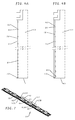
- Figure 4A shows an example where parallel grooves 84 of a particular depth are formed in the rear face 28, and the pitch between adjacent grooves progressively decreases from the point 62 near the LED 40 to the point 70 near the far edge 60 of the panel 12 parallel grooves 84 of the particular depth but a smaller pitch are formed in the rear face 28.
- Figure 4B shows an example where parallel grooves 84 of a particular pitch are formed in the rear face 28, and the depth of the grooves 84 progressively increases from the point 62 near the LED 40 to the point 70 near the far edge 60 of the panel 12. It will be appreciated that the arrangements of Figures 4A and 4B may be combined to provide for surface irregularities with both a non-uniform pitch and a non-uniform depth.
- the glossiness of the rear face 28 may also be rendered non-uniform by other treatments, such as rubbing the face 28 with a rotating wire wheel with varying pressure being applied, rubbing the face 28 with varying grades of abrasive paper, or sand-blasting the rear face 28 with varying exposure times.
- the panel 12 is rectangular. However, the panel may have any regular or irregular shape.
- Figures 5A & B show a second embodiment of the invention with a circular panel 12 having a circular groove 32 for the PCB assembly 14 and compression element 20.
- the heatsink 22 of the second embodiment is a plain circular disc which is secured to the rear of the panel 12 by screws 86.
- the compression element 20 engages both the plate of the heatsink 22 and the outer edge of the groove 32, the compression element 20 prevents the ingress of any moisture into the region occupied by the PCB assembly 14.
- At least the face of the plate of the heatsink 22 facing the panel 12 is finished as matt white so as to serve the same function as the backing sheet 24 in the first embodiment of the invention.
- connection lead (not shown) in the second embodiment may enter the panel through a grommet in the plate of the heatsink 22 or in the outer wall of the groove 32. Because of the circular shape of the panel 12, the required non-uniformity of the glossiness of the rear face 28 of the panel 12 in order to achieve uniform illumination may be less pronounced than in the case of the first embodiment. The non-uniformity will be rotationally symmetrical through any angle about the centre of the panel 12.
- Figures 6A & B show a third embodiment of the invention which is similar to the second embodiment except that the panel 12 is elliptical.
- the required non-unifomity of the glossiness of the rear face 28 of the panel 12 will be more complex than in the first and second embodiments but can be ascertained by trial and error.
- FIG. 7 shows more detail of a PCB assembly 14 which may be used in the embodiments of the invention.
- the PCB assembly 14 comprises a flexible PCB 38 made from Kapton ® .
- the PCB 38 is in the form of a strip many metres long and is divided up into identical sections 88 (three of which are shown in Figure 7 ) separated by perforated break lines 90.
- Each section 88 comprises two connecting pads 42A,B at one end and two connecting pads 42C,D at the opposite end.
- the tracks of the PCB 38 connect: pad 42A to pad 42C; pad 42B to pad 42D; and pad 42B to pad 42C via a plurality of LEDs 40 and a current regulator 44 in series.
- the tracks of the PCB 38 connect: pads 42A and 42C of the adjacent sections 88; and pads 42B and 42D of adjacent sections.
- the PCB assembly 14 can therefore be cut or snapped apart along a break line 90 to form any desired length of assembly 14 which is an integer multiple of the length of each section 88.
- the electricity supply can then be connected to the pads 42A,B at one end of the length of PCB assembly 14, and the pads 42C,D at the opposite end may be left unconnected, connected to another PCB assembly 14 or connected back to the pads 42A,B at the first end in a ring.
- Each current regulator 44 serves to regulate the current through the LEDs 40 in its section 88 to a desired value provided that the voltage supplied to the section 88 is sufficiently high for the regulator 44 not to drop out and provided the supply voltage is not too high to overload the regulator 44. Uniform illumination of the LEDs 40 can therefore be achieved despite variation in the supply voltage, voltage drops along the length of the PCB assembly 14, and the number of sections 88 in the PCB assembly 14.
- the current regulators 44 are adjustable, and further interconnected connecting pads are provided at each end of each section 88 for receiving a control voltage and supplying the control voltage to each current regulator 44.
- the panel 12 may be clear or tinted.
- the front face 58 of the panel 12 may be unmarked so that substantially the whole of the panel 12 is illuminated.
- the front face 58 of the panel may be masked with an opaque or contrastingly-coloured graphic in a conventional manner.
- the colours of the LEDs 40 may be chosen to suit the colours of the graphic.
- the LEDs 40 may be driven to provide a flashing sign, and a dimming arrangement may be provided, which may be responsive to ambient light.
- the panel assembly 10 may be incorporated into another structure.
Landscapes
- Physics & Mathematics (AREA)
- General Physics & Mathematics (AREA)
- Optics & Photonics (AREA)
- Engineering & Computer Science (AREA)
- Mechanical Engineering (AREA)
- Life Sciences & Earth Sciences (AREA)
- Sustainable Development (AREA)
- Thermal Sciences (AREA)
- General Engineering & Computer Science (AREA)
- Planar Illumination Modules (AREA)
- Illuminated Signs And Luminous Advertising (AREA)
Abstract
Description
- This invention relates to light guide panel assemblies.
- Such panel assemblies can be used to provide illuminated signs, such as road signs, which may convey a message by virtue of their shape or by masking provided on the panel assembly. They may also be used for back-lighting of displays such as liquid crystal computer screens or television screens.
- A conventional panel assembly of this type comprises a translucent panel (for example of acrylic) and at least one light-emitting device (such as an light emitting diode, or LED) arranged for producing a divergent beam of light and projecting the light into the panel from a light-receiving edge of the panel. As the light passes through the panel, it is internally reflected by the front and rear faces of the panel and at least some of the light is transmitted by at least one light-emitting surface portion of at least one of the faces so as to illuminate that surface portion. At least one other surface portion of that face may be opaque so that an illuminated pattern is formed on that face. Alternatively, substantially all of one or each face may be light-emitting, so that the whole face (which may have a particular shape such as a direction arrow) is illuminated.
- Although high-power LEDs are reasonably efficient at converting electrical energy into light energy, they do produce heat and can become hot. The hotter the temperature at which an LED is run, the shorter its life. It is therefore desirable to conduct the heat away from the LED.
- It is desirable that the light emitting device(s) and any other electrical components contained in the panel assembly are protected against the ingress of moisture.
- It is also desirable that the light-emitting face of the panel assembly provides uniform illumination (other than in areas where the face is intended to be masked). However, generally speaking, the further the light travels through the panel from the light-emitting device, the less intense it becomes. Also, if the light-emitting device(s) are not properly positioned, for example being canted over, they can produce aberrations in the illumination.
- An aim of the present invention, or at least of specific embodiments of it, is to provide a light guide panel assembly which can: conduct heat effectively away from the light-emitting device(s); establish and maintain proper positioning of the light emitting device(s); provide a seal against ingress of moisture to the light-emitting devices; provide substantially uniform illumination of the light-emitting face of the panel assembly (other than in areas where the face is intended to be masked); and accomplish all of the aforesaid in a simple, convenient and inexpensive manner.
- In accordance with a first aspect of the present invention, there is provided a light guide panel assembly comprising: a translucent panel; a light-emitting device (such as an LED) arranged for producing a divergent beam of light and projecting the light into the panel from a light-receiving edge of the panel; a heatsink; and a compressible, thermally-conductive element disposed in compression against the heatsink and so as to urge the light-emitting device against the light-receiving edge of the panel and to provide a thermal pathway between the light-emitting device and the heatsink. The compressible element therefore serves the dual purposes of holding the light-emitting device in place and also assisting in conducting heat away from it. In some embodiments, it can also serve as a seal to prevent ingress of moisture to the light-emitting device.
- The light emitting device is preferably one of a plurality of such light-emitting devices mounted on one face of a common, elongate circuit board, and the compressible element is preferably elongate and is compressed against the heatsink and an opposite face of the circuit board.
- The light-receiving edge of the panel may include at least a portion which is not straight, in which case the circuit board is preferably flexible and conforms to the shape of the light-receiving edge of the panel. This conveniently enables complex shapes of panel assembly to be provided.
- The circuit board may have connection pads at each end of the circuit board, so that a plurality of the circuit boards can be daisy-chained together in a single panel assembly and/or in separate panel assemblies.
- The light-receiving edge of the panel is preferably formed by a side wall of a groove formed in one face of the panel, the light-emitting device(s) and compressible element being disposed in the groove, therefore enabling the opposite face of the panel to be uninterrupted. In this case, the compressible element is preferably disposed in compression against a bottom wall of the groove and against an opposite side wall of the groove, with the heatsink closing off the groove at the rear face of the panel.
- A front face of the panel preferably has at least one light-emitting surface portion which specularly reflects and transmits light incident thereon from within the panel, and a rear face of the panel preferably specularly reflects and scatteringly reflects light incident thereon from within the panel. This enables the panel to act as a light guide and to illuminate the front face.
- The rear face of the panel preferably specularly reflects and scatteringly reflects light incident thereon from within the panel with a ratio of specular to scattering reflection which is non-uniform across the rear face of the panel, preferably so as to cause substantially uniform illumination of the front face.
- This latter feature may be provided independently of other features of the first aspect of the invention. Therefore, in accordance with a second aspect of the invention, there is provided a light guide panel assembly comprising a translucent panel and a light-emitting device arranged for producing a divergent beam of light and projecting the light into the panel from a light-receiving edge of the panel, wherein: a front face of the panel has at least one light-emitting surface portion which specularly reflects and transmits light incident thereon from within the panel; and a rear face of the panel specularly reflects and scatteringly reflects light incident thereon from within the panel with a ratio of specular to scattering reflection which is non-uniform across the rear face of the panel.
- The non-uniform reflection ratio may be provided by the rear face of the panel having a smooth surface interrupted by surface irregularities having a density which is non-uniform across the rear face of the panel. In particular, the surface irregularities may have depths which are non-uniform across the rear face of the panel and/or pitches relative to adjacent irregularities which are non-uniform across the rear face of panel. The surface irregularities may be formed by grooves in the rear surface of the panel. The grooves may be substantially straight and parallel, especially in the case of a rectangular panel illuminated along one edge, and/or they may be curved and/or non-parallel and/or non-concentric in the case of more complex shapes of panel.
- The panel assembly preferably further includes a scatteringly reflective surface disposed against the rear face of the panel so that any light that escapes through the rear face is reflected back to the rear face. In the case where a heatsink is provided, the scatteringly reflective surface may be provided by the heatsink.
- The or each light-emitting surface portion of the front face of the panel preferably (a) specularly reflects substantially all light incident thereon from within the panel at an angle of incidence greater than the critical angle; and (b) transmits substantially all light incident thereon from within the panel at an angle of incidence less than the critical angle.
- Specific embodiments of the present invention will now be described, purely by way of example, with reference to the accompanying drawings, in which:
- Figure 1
- is an exploded isometric view of a first embodiment of light guide panel assembly with its centre portion cut away;
- Figure 2A-C
- are sectioned side views of the light guide panel assembly of
Figure 1 , exploded inFigure 2A , partly assembled inFigure 2B , and fully assembled inFigure 2C ; - Figures 3A-D
- are side views of the panel assembly of
Figures 1 and2 showing sample light rays resulting in emission of light from four different regions on a front face of the panel assembly; - Figure 4A & B
- are side views on a larger scale showing two different arrangements of surface irregularities on two portions of the rear face of the panel assembly;
- Figures 5A & B
- are a sectioned side view and a sectioned underplan view, respectively, of a second embodiment of light guide panel assembly;
- Figures 6A & B
- are a sectioned side view and a sectioned underplan view, respectively, of a third embodiment of light guide panel assembly; and
- Figure 7
- is an isometric view of a modified printed circuit board assembly for use in the embodiments of the invention.
- Referring to
Figures 1 to 2C , the first embodiment of lightguide panel assembly 10 comprises apanel 12, a printed circuit board (PCB)assembly 14, a two-core connection lead 16, ablanking plug 18, acompression element 20, aheatsink 22 and a backing sheet 24 (not shown inFigure 1 ). - The
panel 12 is generally rectangular and is made of acrylic. Arabbet 26 is formed in therear face 28 and oneedge 30 of thepanel 12. Adeep groove 32 is formed in the rabbeted portion of thepanel 12 and extends almost to theends 34 of thepanel 12. Theinnermost edge 52 of thedeep groove 32 is preferably polished.Smaller grooves 36 are formed between the ends of thedeep groove 32 and theends 34 of thepanel 12. - The
PCB assembly 14 comprises aflexible PCB 38 made from Kapton® or similar material. The PCB 38 is in the form of a strip having a length slightly less than the length of thegroove 32 in thepanel 12 and a width slightly less than the depth of thegroove 32 in thepanel 12. A plurality of flat-faced surface-mount LEDs 40 are mounted on thePCB 38. The PCB 38 has a pair of connectingpads 42 at each of its ends. ThePCB 38 may also carryother components 44 such as voltage-dropping resistors and/or current regulators. TheLEDs 40, connectingpads 42 andother components 44 are connected by tracks (not shown) of thePCB 38 so that when the connectingpads 42 at one end of thePCB 38 are connected to a electrical supply of a particular voltage and polarity, an appropriate electrical current passes through eachLED 40 to illuminate it, and also the supply voltage is fed to the connectingpads 42 at the opposite end of thePCB 38. - The
connection lead 16 has a mouldedresilient grommet 46 adjacent one end which is a tight fit in thesmaller groove 36 at oneend 34 of thepanel 12 and which naturally protrudes slightly above thegroove 36. During assembly of thepanel assembly 10, thecores 48 of thelead 16 are soldered to the connectingpads 42 at the adjacent end of thePCB 38. The other end of thelead 16 is connected to an electrical supply, such as a battery pack or a mains-to-DC adapter. The blankingplug 18 is a tight fit in thesmaller groove 36 at theopposite end 34 of thepanel 12 and naturally protrudes slightly above thegroove 36. As an alternative to using the blankingplug 18, thesmaller groove 36 at thatend 34 of thepanel 12 may be omitted. Alternatively, a further connection lead may be fitted similarly to theconnection lead 16 and soldered to the connectingpads 42 at the adjacent end of thePCB 38 so that electricity can be fed to another light guide panel assembly. - The
compression element 20 is a tubular O-rope formed from doped silicone rubber which is resilient, has a high thermal conductivity and is waterproof. For example, the compression element may be made of Primasil PR910/1388 available from Primasil Silicones, HR4 8QU, United Kingdom, and having a thermal conductivity of about 1.5 W.m-1.K-1. The length of thecompression element 20 is slightly longer than the length of thedeep grove 32. Thecompression element 20 has an outer diameter which is slightly greater than the depth of thedeep groove 32 and slightly greater than the width of thedeep groove 32 less the height of thePCB assembly 14. - The
heatsink 22 is formed from a plate of aluminium alloy having a width equal to the width of therabbet 26 and a length equal to the length of thepanel 12 between its ends 34. Theheatsink 22 may be plain or (as shown) it may be formed withfins 50 on one face. - The
backing sheet 24 is formed from plastics film having a matt-white self-adhesive surface. Thebacking sheet 24 is the same size as the rear non-rabbeted portion of thepanel 12. - Referring in particular to
Figures 2A & B , during assembly of thepanel assembly 10, thePCB assembly 14 is placed in thedeep groove 32 with the light-emitting faces of theLEDs 40 abutting the polishedinnermost edge 52 of thedeep groove 32, and thegrommet 46 of theconnection lead 16 and the blankingplug 18 are squeezed into thesmaller grooves 36. Thecompression element 20 is then squeezed into thedeep groove 32 so that it abuts the rear of thePCB assembly 14, theoutermost edge 54 of thegroove 32 and the bottom 56 of thegroove 32. As can be seen inFigure 2B , thecompression element 20 naturally protrudes from thedeep groove 32. Then, adhesive is applied to the plain face of theheatsink 22 and/or to therabbet 26, and theheatsink 22 is pressed into therabbet 26 so as to compress thecompression element 20 into thedeep groove 32, as shown inFigure 2C , and also compress thegrommet 46 and blankingplug 18 into thesmaller grooves 36. External pressure is maintained until the adhesive has cured. Also, as shown inFigure 2C , thebacking sheet 24 is adhered to the rear non-rabbeted portion of thepanel 12. - It will therefore be appreciated that the thermally-
conductive compression element 20 urges itself into good contact with the rear of thePCB assembly 14 and theheatsink 22 so as to provide a good thermal path between the two. Thecompression element 20 also urges the light-emitting faces of theLEDs 40 into contact with theedge 52 of thegroove 32. Moreover, thecompression element 20 serves to prevent any moisture which enters between thepanel 12 and theheatsink 22 at theedge 30 of thepanel 12 from reaching thePCB assembly 38. - In operation, the
LEDs 40 each produce a divergent beam having a viewing half-angle of, for example, 30 to 40 degrees and possibly greater. The acrylic material of thepanel 12 has a refractive index of about 1.49, and therefore the critical angle at the acrylic-air interface is about 42 degrees. Thefront face 58 of thepanel 12 is polished so that: - substantially all light incident on the
front face 58 from within thepanel 12 is specularly reflected if the angle of incidence is greater than the critical angle; - substantially all light incident on the
front face 58 from within thepanel 12 is transmitted out of the panel if the angle of incidence is less than the critical angle; and - no substantial amount of light incident on the
front face 58 from within thepanel 12 is scatteringly reflected. - a proportion of light incident on the
rear face 28 from within thepanel 12 is specularly reflected; and - a proportion of light incident on the
rear face 28 from within thepanel 12 is specularly reflected either directly or by being transmitted through therear face 28 and then being specularly reflected back to thepanel 12 by the matt white surface of thebacking sheet 24. - The
outer edge 60 of thepanel 12 remote from theLEDs 40 may be substantially totally absorbent to light or may be slightly reflective. Thesides 34 of the panel are preferably reflective. - Referring to
Figures 3A-D and considering only light rays travelling in the plane of the paper, it will be seen that at a point 62 (Figure 3A ) on therear face 28 of thepanel 12 adjacent theLED 40, substantially the only incident light is ahigh intensity ray 64 received directly from theLED 40. A proportion of this light (i.e. of lower intensity than the ray 64) is specularly reflected, as shown byray 66, and a proportion is scatteringly reflected, as shown by therays 68, and illuminates thepanel 12 in theregion 69. By contrast, at a point 70 (Figure 3D ) on therear face 28 of thepanel 12 adjacent thefar edge 60 of thepanel 12, the incident light comprises: - a
ray 72 received directly from theLED 40; - a
ray 74 received after one specular reflection from thefront face 58; - a
ray 76 received after one reflection from therear face 28 and one specular reflection from thefront face 58; and - a number of
other rays 78 received after multiple reflections from the front and rear faces 58,28 of thepanel 12. - Each of these rays 72-78 is of lower intensity than the
ray 64 received at point 62 (Figure 3A ) due to the greater distance from theLED 40. Furthermore, the intensity of therays rear face 28 of thepanel 12. Preferably, at thepoint 70 adjacent thefar edge 60, therear face 28 of thepanel 12 is totally matt, so that none of the rays 72-78 is specularly reflected, in which case all of the rays 72-78 are scatteringly reflected as shown by therays 80, and illuminate the panel in the region 82. - To a first order approximation, the intensity of the
ray 64 incident on thepoint 62 adjacent theLED 40 is substantially greater than the total intensity of the rays 72-78 incident onpoint 70 adjacent thefar edge 60 of thepanel 12. Therefore, therear face 28 of thepanel 12 needs to be substantially more glossy (i.e. specularly reflect a greater proportion of light) atpoint 62 than atpoint 70 in order that the illumination provided by therays 68 inregion 69 is substantially equal to the illumination provided by therays 80 in region 82. Indeed, to a first order approximation, the required glossiness of therear face 28 of thepanel 12 is related to the inverse of the distance from theLED 40. However, other factors affect uniform illumination of thefront face 58 of thepanel 12, notably the radiation pattern of the LEDs 40 (i.e. the variation of intensity with viewing angle) and edge effects. Therefore, the non-uniformity of glossiness of therear face 28 of thepanel 12 that is required in order to achieve uniform illumination of thefront face 58 of thepanel 12 is best determined by trial and error. - The non-uniform glossiness of the
rear face 28 of thepanel 12 may be achieved in a number of ways. For example, discrete formations may be provided in therear face 28, such as grooves cut or laser-engraved into therear face 28.Figure 4A shows an example whereparallel grooves 84 of a particular depth are formed in therear face 28, and the pitch between adjacent grooves progressively decreases from thepoint 62 near theLED 40 to thepoint 70 near thefar edge 60 of thepanel 12parallel grooves 84 of the particular depth but a smaller pitch are formed in therear face 28.Figure 4B shows an example whereparallel grooves 84 of a particular pitch are formed in therear face 28, and the depth of thegrooves 84 progressively increases from thepoint 62 near theLED 40 to thepoint 70 near thefar edge 60 of thepanel 12. It will be appreciated that the arrangements ofFigures 4A and 4B may be combined to provide for surface irregularities with both a non-uniform pitch and a non-uniform depth. - Instead of providing discrete regular formations, the glossiness of the
rear face 28 may also be rendered non-uniform by other treatments, such as rubbing theface 28 with a rotating wire wheel with varying pressure being applied, rubbing theface 28 with varying grades of abrasive paper, or sand-blasting therear face 28 with varying exposure times. - In the first embodiment described above, the
panel 12 is rectangular. However, the panel may have any regular or irregular shape. - For example,
Figures 5A & B show a second embodiment of the invention with acircular panel 12 having acircular groove 32 for thePCB assembly 14 andcompression element 20. Because thePCB 38 andcompression element 20 are flexible, they can both readily be formed into circles. Theheatsink 22 of the second embodiment is a plain circular disc which is secured to the rear of thepanel 12 byscrews 86. It will be noted that because thecompression element 20 engages both the plate of theheatsink 22 and the outer edge of thegroove 32, thecompression element 20 prevents the ingress of any moisture into the region occupied by thePCB assembly 14. At least the face of the plate of theheatsink 22 facing thepanel 12 is finished as matt white so as to serve the same function as thebacking sheet 24 in the first embodiment of the invention. The connection lead (not shown) in the second embodiment may enter the panel through a grommet in the plate of theheatsink 22 or in the outer wall of thegroove 32. Because of the circular shape of thepanel 12, the required non-uniformity of the glossiness of therear face 28 of thepanel 12 in order to achieve uniform illumination may be less pronounced than in the case of the first embodiment. The non-uniformity will be rotationally symmetrical through any angle about the centre of thepanel 12. -
Figures 6A & B show a third embodiment of the invention which is similar to the second embodiment except that thepanel 12 is elliptical. In this case, the required non-unifomity of the glossiness of therear face 28 of thepanel 12 will be more complex than in the first and second embodiments but can be ascertained by trial and error. -
Figure 7 shows more detail of aPCB assembly 14 which may be used in the embodiments of the invention. As described above, thePCB assembly 14 comprises aflexible PCB 38 made from Kapton®. ThePCB 38 is in the form of a strip many metres long and is divided up into identical sections 88 (three of which are shown inFigure 7 ) separated by perforated break lines 90. Eachsection 88 comprises two connectingpads 42A,B at one end and two connectingpads 42C,D at the opposite end. In eachsection 88, the tracks of thePCB 38 connect: pad 42A to pad 42C; pad 42B to pad 42D; and pad 42B to pad 42C via a plurality ofLEDs 40 and acurrent regulator 44 in series. Also, across eachbreak line 90, the tracks of thePCB 38 connect:pads adjacent sections 88; andpads PCB assembly 14 can therefore be cut or snapped apart along abreak line 90 to form any desired length ofassembly 14 which is an integer multiple of the length of eachsection 88. The electricity supply can then be connected to thepads 42A,B at one end of the length ofPCB assembly 14, and thepads 42C,D at the opposite end may be left unconnected, connected to anotherPCB assembly 14 or connected back to thepads 42A,B at the first end in a ring. Eachcurrent regulator 44 serves to regulate the current through theLEDs 40 in itssection 88 to a desired value provided that the voltage supplied to thesection 88 is sufficiently high for theregulator 44 not to drop out and provided the supply voltage is not too high to overload theregulator 44. Uniform illumination of theLEDs 40 can therefore be achieved despite variation in the supply voltage, voltage drops along the length of thePCB assembly 14, and the number ofsections 88 in thePCB assembly 14. - In a modification to the
PCB assembly 14 ofFigure 7 , thecurrent regulators 44 are adjustable, and further interconnected connecting pads are provided at each end of eachsection 88 for receiving a control voltage and supplying the control voltage to eachcurrent regulator 44. - In all of the embodiments described above, the
panel 12 may be clear or tinted. Also, thefront face 58 of thepanel 12 may be unmarked so that substantially the whole of thepanel 12 is illuminated. Alternatively, thefront face 58 of the panel may be masked with an opaque or contrastingly-coloured graphic in a conventional manner. The colours of theLEDs 40 may be chosen to suit the colours of the graphic. TheLEDs 40 may be driven to provide a flashing sign, and a dimming arrangement may be provided, which may be responsive to ambient light. Thepanel assembly 10 may be incorporated into another structure. - It should be noted that the embodiments of the invention has been described above purely by way of example and that many other modifications and developments may be made thereto within the scope of the present invention.
Claims (15)
- A light guide panel assembly (10) comprising:a translucent panel (12);a light-emitting device (40) arranged for producing a divergent beam of light andprojecting the light into the panel from a light-receiving edge (52) of the panel;a heatsink (22); anda compressible, thermally-conductive element (20) disposed in compression against the heatsink and so as to urge the light-emitting device against the light-receiving edge of the panel and to provide a thermal pathway between the light-emitting device and the heatsink.
- A light guide panel assembly as claimed in claim 1, wherein:the light emitting device is one of a plurality of such light-emitting devices mounted on one face of a common, elongate circuit board (38); andthe compressible element is elongate and is compressed against the heatsink and an opposite face of the circuit board.
- A light guide panel assembly as claimed in claim 2, wherein:the light-receiving edge of the panel includes at least a portion which is not straight; andthe circuit board is flexible and conforms to the shape of the light-receiving edge of the panel.
- A light guide panel assembly as claimed in claim 2 or 3, wherein:the circuit board has connection pads (42) at each end of the circuit board.
- A light guide panel assembly as claimed in any preceding claim, wherein:the light-receiving edge of the panel is formed by a side wall of a groove (32) formed in one face (28) of the panel; andthe light-emitting device(s) and compressible element are disposed in the groove.
- A light guide panel assembly as claimed in claim 5, wherein:the compressible element is disposed in compression against a bottom wall (56) of the groove and against an opposite side wall (54) of the groove; andthe heatsink closes the groove at the rear face of the panel.
- A light guide panel assembly as claimed in any preceding claim, wherein:a front face (58) of the panel has at least one light-emitting surface portion which specularly reflects and transmits light incident thereon from within the panel;a rear face (28) of the panel specularly reflects and scatteringly reflects light incident thereon from within the panel.
- A light guide panel assembly as claimed in any preceding claim, wherein:the rear face of the panel specularly reflects and scatteringly reflects light incident thereon from within the panel with a ratio of specular to scattering reflection which is non-uniform across the rear face of the panel.
- A light guide panel assembly (10) comprising:a translucent panel (12); anda light-emitting device (40) arranged for producing a divergent beam of light andprojecting the light into the panel from a light-receiving edge (52) of the panel;wherein:a front face (58) of the panel has at least one light-emitting surface portion which specularly reflects and transmits light incident thereon from within the panel; anda rear face (28) of the panel specularly reflects and scatteringly reflects light incident thereon from within the panel with a ratio of specular to scattering reflection which is non-uniform across the rear face of the panel.
- A light guide panel assembly as claimed in claim 8 or 9, wherein:the rear face of the panel has a smooth surface interrupted by surface irregularities (84) having a density which is non-uniform across the rear face of the panel.
- A light guide panel assembly as claimed in claim 10, wherein:the surface irregularities have (i) depths, and/or (ii) pitches relative to adjacent irregularities, which are non-uniform across the rear face of panel.
- A light guide panel assembly as claimed in claim 10 or 11, wherein:the surface irregularities are formed by grooves (84) in the rear surface of the panel.
- A light guide panel assembly as claimed in any of claims 7 to 12, further including:a scatteringly reflective surface (24) disposed against the rear face of the panel.
- A light guide panel assembly as claimed in claim 13 when directly or indirectly dependent on claim 1, wherein:the scatteringly reflective surface is provided by the heatsink.
- A light guide panel assembly as claimed in any of claims 7 to 14, wherein:the or each light-emitting surface portion of the front face of the panel:specularly reflects substantially all light incident thereon from within the panel at an angle of incidence greater than the critical angle; andtransmits substantially all light incident thereon from within the panel at an angle of incidence less than the critical angle.
Applications Claiming Priority (1)
| Application Number | Priority Date | Filing Date | Title |
|---|---|---|---|
| GB1006375.8A GB2479590B (en) | 2010-04-16 | 2010-04-16 | Light guide panel assembly |
Publications (3)
| Publication Number | Publication Date |
|---|---|
| EP2378327A2 true EP2378327A2 (en) | 2011-10-19 |
| EP2378327A3 EP2378327A3 (en) | 2011-12-07 |
| EP2378327B1 EP2378327B1 (en) | 2018-03-14 |
Family
ID=42245318
Family Applications (1)
| Application Number | Title | Priority Date | Filing Date |
|---|---|---|---|
| EP11162511.7A Not-in-force EP2378327B1 (en) | 2010-04-16 | 2011-04-14 | Light guide panel assembly |
Country Status (3)
| Country | Link |
|---|---|
| US (1) | US20110255302A1 (en) |
| EP (1) | EP2378327B1 (en) |
| GB (1) | GB2479590B (en) |
Cited By (3)
| Publication number | Priority date | Publication date | Assignee | Title |
|---|---|---|---|---|
| EP2447747A1 (en) * | 2010-10-27 | 2012-05-02 | Young Lighting Technology Corporation | Flat light source module |
| WO2013119692A3 (en) * | 2012-02-06 | 2013-10-31 | Avery Dennison Corporation | Direction active projection |
| WO2014009730A1 (en) | 2012-07-13 | 2014-01-16 | Zeta Specialist Lighting Limited | Solar powered light assembly |
Families Citing this family (4)
| Publication number | Priority date | Publication date | Assignee | Title |
|---|---|---|---|---|
| GB2552807B (en) * | 2016-08-10 | 2019-03-20 | Lightly Tech Limited | A planar LED light source module |
| KR102328543B1 (en) * | 2021-07-09 | 2021-11-18 | 주식회사 필리스 | Surface emitting lumination device |
| KR102327804B1 (en) * | 2021-07-09 | 2021-11-18 | 주식회사 필리스 | surface emitting lumination device |
| US20260160936A1 (en) * | 2024-12-06 | 2026-06-11 | Hannstar Display Corporation | Light guide plate |
Family Cites Families (14)
| Publication number | Priority date | Publication date | Assignee | Title |
|---|---|---|---|---|
| JP3905755B2 (en) * | 2001-12-20 | 2007-04-18 | シャープ株式会社 | Backlight device |
| JP2004127922A (en) * | 2002-07-26 | 2004-04-22 | Ccs Inc | Light irradiation device and manufacturing method thereof |
| TWI257015B (en) * | 2002-12-20 | 2006-06-21 | Hon Hai Prec Ind Co Ltd | Light guide plate and back light system with the same |
| KR100506092B1 (en) * | 2003-04-16 | 2005-08-04 | 삼성전자주식회사 | Light guide panel of edge light type backlight apparatus and edge light type backlight apparatus using the same |
| WO2006137660A2 (en) * | 2005-06-22 | 2006-12-28 | Fawoo Technology Co., Ltd. | Back light unit |
| BRPI0616785A2 (en) * | 2005-10-26 | 2012-04-17 | Fawoo Technology Co Ltd | taillight unit |
| TWI280332B (en) * | 2005-10-31 | 2007-05-01 | Guei-Fang Chen | LED lighting device |
| BRPI0721020A2 (en) * | 2007-01-22 | 2014-07-29 | Sharp Kk | REAR LIGHT DEVICE AND FLAT DISPLAY Using the same |
| WO2008152563A1 (en) * | 2007-06-14 | 2008-12-18 | Koninklijke Philips Electronics N.V. | Accurate light source - optics positioning system and method |
| US7942556B2 (en) * | 2007-06-18 | 2011-05-17 | Xicato, Inc. | Solid state illumination device |
| JP2009245885A (en) * | 2008-03-31 | 2009-10-22 | Sanken Electric Co Ltd | Surface light source device |
| US8028537B2 (en) * | 2009-05-01 | 2011-10-04 | Abl Ip Holding Llc | Heat sinking and flexible circuit board, for solid state light fixture utilizing an optical cavity |
| KR100993059B1 (en) * | 2008-09-29 | 2010-11-08 | 엘지이노텍 주식회사 | Light emitting device |
| US8128262B2 (en) * | 2010-03-30 | 2012-03-06 | Abl Ip Holdings Llc | Lighting applications with light transmissive optic contoured to produce tailored light output distribution |
-
2010
- 2010-04-16 GB GB1006375.8A patent/GB2479590B/en not_active Expired - Fee Related
-
2011
- 2011-04-14 EP EP11162511.7A patent/EP2378327B1/en not_active Not-in-force
- 2011-04-15 US US13/087,926 patent/US20110255302A1/en not_active Abandoned
Non-Patent Citations (1)
| Title |
|---|
| None |
Cited By (5)
| Publication number | Priority date | Publication date | Assignee | Title |
|---|---|---|---|---|
| EP2447747A1 (en) * | 2010-10-27 | 2012-05-02 | Young Lighting Technology Corporation | Flat light source module |
| US8702295B2 (en) | 2010-10-27 | 2014-04-22 | Young Lighting Technology Inc. | Flat light source module |
| WO2013119692A3 (en) * | 2012-02-06 | 2013-10-31 | Avery Dennison Corporation | Direction active projection |
| US9218755B2 (en) | 2012-02-06 | 2015-12-22 | Avery Dennison Corporation | Direction active projection |
| WO2014009730A1 (en) | 2012-07-13 | 2014-01-16 | Zeta Specialist Lighting Limited | Solar powered light assembly |
Also Published As
| Publication number | Publication date |
|---|---|
| US20110255302A1 (en) | 2011-10-20 |
| EP2378327B1 (en) | 2018-03-14 |
| GB2479590A (en) | 2011-10-19 |
| EP2378327A3 (en) | 2011-12-07 |
| GB2479590B (en) | 2016-08-10 |
| GB201006375D0 (en) | 2010-06-02 |
Similar Documents
| Publication | Publication Date | Title |
|---|---|---|
| EP2378327B1 (en) | Light guide panel assembly | |
| CN1912713B (en) | Light source suitable for LCD backlight display | |
| TWI536335B (en) | Light emitting diode display unit and light emitting diode display | |
| CN202093765U (en) | light box | |
| CN101529290B (en) | Luminaire arrangement with a cover layer | |
| CN102072428B (en) | Light emitting diode (LED) daylight lamp | |
| US20180364414A1 (en) | Device and apparatus configured for illuminating an indicium | |
| US20090196071A1 (en) | Lighting system for creating an illuminated surface | |
| JP6640948B2 (en) | Light diffusion using light source | |
| EP1275101A2 (en) | A flexible light track for signage | |
| WO2001084046A1 (en) | Illumination system and display device | |
| EP1407185A1 (en) | Frontlit display | |
| JP2003045214A (en) | Light emitting device | |
| KR101185523B1 (en) | Led flat lighting with an unified guideplate | |
| JP2015195204A (en) | Strip-like led light | |
| US7281834B2 (en) | Method and apparatus for image illumination using self-contained luminaire | |
| US6505946B2 (en) | Spread illumination apparatus | |
| TWM302121U (en) | Light source module | |
| TWI503090B (en) | Protective cover | |
| TW201122579A (en) | Light guiding plate (LGP) device and backlight module using the same | |
| CN201187731Y (en) | LED light guide plate and heat dissipation device thereof | |
| JP4721159B2 (en) | Surface lighting device | |
| US20110146120A1 (en) | Emergency exit indicator incorporating led unit | |
| CN100376966C (en) | light guide plate | |
| CN201795313U (en) | Sheet light with double LED light strips |
Legal Events
| Date | Code | Title | Description |
|---|---|---|---|
| AK | Designated contracting states |
Kind code of ref document: A2 Designated state(s): AL AT BE BG CH CY CZ DE DK EE ES FI FR GB GR HR HU IE IS IT LI LT LU LV MC MK MT NL NO PL PT RO RS SE SI SK SM TR |
|
| AX | Request for extension of the european patent |
Extension state: BA ME |
|
| PUAL | Search report despatched |
Free format text: ORIGINAL CODE: 0009013 |
|
| PUAI | Public reference made under article 153(3) epc to a published international application that has entered the european phase |
Free format text: ORIGINAL CODE: 0009012 |
|
| AK | Designated contracting states |
Kind code of ref document: A3 Designated state(s): AL AT BE BG CH CY CZ DE DK EE ES FI FR GB GR HR HU IE IS IT LI LT LU LV MC MK MT NL NO PL PT RO RS SE SI SK SM TR |
|
| AX | Request for extension of the european patent |
Extension state: BA ME |
|
| RIC1 | Information provided on ipc code assigned before grant |
Ipc: G02B 6/00 20060101AFI20111103BHEP |
|
| 17P | Request for examination filed |
Effective date: 20120926 |
|
| RIN1 | Information on inventor provided before grant (corrected) |
Inventor name: DENT, NIGEL ALASTAIR Inventor name: SHADBOLT, PHILIP DAVID |
|
| RAP1 | Party data changed (applicant data changed or rights of an application transferred) |
Owner name: ZETA SPECIALIST LIGHTING LIMITED |
|
| 17Q | First examination report despatched |
Effective date: 20130712 |
|
| GRAP | Despatch of communication of intention to grant a patent |
Free format text: ORIGINAL CODE: EPIDOSNIGR1 |
|
| STAA | Information on the status of an ep patent application or granted ep patent |
Free format text: STATUS: GRANT OF PATENT IS INTENDED |
|
| INTG | Intention to grant announced |
Effective date: 20171218 |
|
| GRAS | Grant fee paid |
Free format text: ORIGINAL CODE: EPIDOSNIGR3 |
|
| GRAA | (expected) grant |
Free format text: ORIGINAL CODE: 0009210 |
|
| STAA | Information on the status of an ep patent application or granted ep patent |
Free format text: STATUS: THE PATENT HAS BEEN GRANTED |
|
| AK | Designated contracting states |
Kind code of ref document: B1 Designated state(s): AL AT BE BG CH CY CZ DE DK EE ES FI FR GB GR HR HU IE IS IT LI LT LU LV MC MK MT NL NO PL PT RO RS SE SI SK SM TR |
|
| REG | Reference to a national code |
Ref country code: GB Ref legal event code: FG4D |
|
| REG | Reference to a national code |
Ref country code: AT Ref legal event code: REF Ref document number: 979436 Country of ref document: AT Kind code of ref document: T Effective date: 20180315 Ref country code: CH Ref legal event code: EP |
|
| REG | Reference to a national code |
Ref country code: IE Ref legal event code: FG4D |
|
| REG | Reference to a national code |
Ref country code: DE Ref legal event code: R096 Ref document number: 602011046427 Country of ref document: DE |
|
| REG | Reference to a national code |
Ref country code: NL Ref legal event code: MP Effective date: 20180314 |
|
| REG | Reference to a national code |
Ref country code: LT Ref legal event code: MG4D |
|
| PG25 | Lapsed in a contracting state [announced via postgrant information from national office to epo] |
Ref country code: FI Free format text: LAPSE BECAUSE OF FAILURE TO SUBMIT A TRANSLATION OF THE DESCRIPTION OR TO PAY THE FEE WITHIN THE PRESCRIBED TIME-LIMIT Effective date: 20180314 Ref country code: CY Free format text: LAPSE BECAUSE OF FAILURE TO SUBMIT A TRANSLATION OF THE DESCRIPTION OR TO PAY THE FEE WITHIN THE PRESCRIBED TIME-LIMIT Effective date: 20180314 Ref country code: LT Free format text: LAPSE BECAUSE OF FAILURE TO SUBMIT A TRANSLATION OF THE DESCRIPTION OR TO PAY THE FEE WITHIN THE PRESCRIBED TIME-LIMIT Effective date: 20180314 Ref country code: HR Free format text: LAPSE BECAUSE OF FAILURE TO SUBMIT A TRANSLATION OF THE DESCRIPTION OR TO PAY THE FEE WITHIN THE PRESCRIBED TIME-LIMIT Effective date: 20180314 Ref country code: NO Free format text: LAPSE BECAUSE OF FAILURE TO SUBMIT A TRANSLATION OF THE DESCRIPTION OR TO PAY THE FEE WITHIN THE PRESCRIBED TIME-LIMIT Effective date: 20180614 Ref country code: ES Free format text: LAPSE BECAUSE OF FAILURE TO SUBMIT A TRANSLATION OF THE DESCRIPTION OR TO PAY THE FEE WITHIN THE PRESCRIBED TIME-LIMIT Effective date: 20180314 |
|
| REG | Reference to a national code |
Ref country code: AT Ref legal event code: MK05 Ref document number: 979436 Country of ref document: AT Kind code of ref document: T Effective date: 20180314 |
|
| PG25 | Lapsed in a contracting state [announced via postgrant information from national office to epo] |
Ref country code: BG Free format text: LAPSE BECAUSE OF FAILURE TO SUBMIT A TRANSLATION OF THE DESCRIPTION OR TO PAY THE FEE WITHIN THE PRESCRIBED TIME-LIMIT Effective date: 20180614 Ref country code: SE Free format text: LAPSE BECAUSE OF FAILURE TO SUBMIT A TRANSLATION OF THE DESCRIPTION OR TO PAY THE FEE WITHIN THE PRESCRIBED TIME-LIMIT Effective date: 20180314 Ref country code: LV Free format text: LAPSE BECAUSE OF FAILURE TO SUBMIT A TRANSLATION OF THE DESCRIPTION OR TO PAY THE FEE WITHIN THE PRESCRIBED TIME-LIMIT Effective date: 20180314 Ref country code: RS Free format text: LAPSE BECAUSE OF FAILURE TO SUBMIT A TRANSLATION OF THE DESCRIPTION OR TO PAY THE FEE WITHIN THE PRESCRIBED TIME-LIMIT Effective date: 20180314 Ref country code: GR Free format text: LAPSE BECAUSE OF FAILURE TO SUBMIT A TRANSLATION OF THE DESCRIPTION OR TO PAY THE FEE WITHIN THE PRESCRIBED TIME-LIMIT Effective date: 20180615 |
|
| PG25 | Lapsed in a contracting state [announced via postgrant information from national office to epo] |
Ref country code: RO Free format text: LAPSE BECAUSE OF FAILURE TO SUBMIT A TRANSLATION OF THE DESCRIPTION OR TO PAY THE FEE WITHIN THE PRESCRIBED TIME-LIMIT Effective date: 20180314 Ref country code: PL Free format text: LAPSE BECAUSE OF FAILURE TO SUBMIT A TRANSLATION OF THE DESCRIPTION OR TO PAY THE FEE WITHIN THE PRESCRIBED TIME-LIMIT Effective date: 20180314 Ref country code: NL Free format text: LAPSE BECAUSE OF FAILURE TO SUBMIT A TRANSLATION OF THE DESCRIPTION OR TO PAY THE FEE WITHIN THE PRESCRIBED TIME-LIMIT Effective date: 20180314 Ref country code: AL Free format text: LAPSE BECAUSE OF FAILURE TO SUBMIT A TRANSLATION OF THE DESCRIPTION OR TO PAY THE FEE WITHIN THE PRESCRIBED TIME-LIMIT Effective date: 20180314 Ref country code: EE Free format text: LAPSE BECAUSE OF FAILURE TO SUBMIT A TRANSLATION OF THE DESCRIPTION OR TO PAY THE FEE WITHIN THE PRESCRIBED TIME-LIMIT Effective date: 20180314 Ref country code: IT Free format text: LAPSE BECAUSE OF FAILURE TO SUBMIT A TRANSLATION OF THE DESCRIPTION OR TO PAY THE FEE WITHIN THE PRESCRIBED TIME-LIMIT Effective date: 20180314 |
|
| REG | Reference to a national code |
Ref country code: DE Ref legal event code: R119 Ref document number: 602011046427 Country of ref document: DE |
|
| PG25 | Lapsed in a contracting state [announced via postgrant information from national office to epo] |
Ref country code: SM Free format text: LAPSE BECAUSE OF FAILURE TO SUBMIT A TRANSLATION OF THE DESCRIPTION OR TO PAY THE FEE WITHIN THE PRESCRIBED TIME-LIMIT Effective date: 20180314 Ref country code: SK Free format text: LAPSE BECAUSE OF FAILURE TO SUBMIT A TRANSLATION OF THE DESCRIPTION OR TO PAY THE FEE WITHIN THE PRESCRIBED TIME-LIMIT Effective date: 20180314 Ref country code: CZ Free format text: LAPSE BECAUSE OF FAILURE TO SUBMIT A TRANSLATION OF THE DESCRIPTION OR TO PAY THE FEE WITHIN THE PRESCRIBED TIME-LIMIT Effective date: 20180314 Ref country code: AT Free format text: LAPSE BECAUSE OF FAILURE TO SUBMIT A TRANSLATION OF THE DESCRIPTION OR TO PAY THE FEE WITHIN THE PRESCRIBED TIME-LIMIT Effective date: 20180314 |
|
| REG | Reference to a national code |
Ref country code: CH Ref legal event code: PL |
|
| REG | Reference to a national code |
Ref country code: BE Ref legal event code: MM Effective date: 20180430 |
|
| PG25 | Lapsed in a contracting state [announced via postgrant information from national office to epo] |
Ref country code: PT Free format text: LAPSE BECAUSE OF FAILURE TO SUBMIT A TRANSLATION OF THE DESCRIPTION OR TO PAY THE FEE WITHIN THE PRESCRIBED TIME-LIMIT Effective date: 20180716 |
|
| PLBE | No opposition filed within time limit |
Free format text: ORIGINAL CODE: 0009261 |
|
| STAA | Information on the status of an ep patent application or granted ep patent |
Free format text: STATUS: NO OPPOSITION FILED WITHIN TIME LIMIT |
|
| REG | Reference to a national code |
Ref country code: IE Ref legal event code: MM4A |
|
| PG25 | Lapsed in a contracting state [announced via postgrant information from national office to epo] |
Ref country code: MC Free format text: LAPSE BECAUSE OF FAILURE TO SUBMIT A TRANSLATION OF THE DESCRIPTION OR TO PAY THE FEE WITHIN THE PRESCRIBED TIME-LIMIT Effective date: 20180314 Ref country code: LU Free format text: LAPSE BECAUSE OF NON-PAYMENT OF DUE FEES Effective date: 20180414 Ref country code: DE Free format text: LAPSE BECAUSE OF NON-PAYMENT OF DUE FEES Effective date: 20181101 Ref country code: DK Free format text: LAPSE BECAUSE OF FAILURE TO SUBMIT A TRANSLATION OF THE DESCRIPTION OR TO PAY THE FEE WITHIN THE PRESCRIBED TIME-LIMIT Effective date: 20180314 |
|
| 26N | No opposition filed |
Effective date: 20181217 |
|
| GBPC | Gb: european patent ceased through non-payment of renewal fee |
Effective date: 20180614 |
|
| PG25 | Lapsed in a contracting state [announced via postgrant information from national office to epo] |
Ref country code: SI Free format text: LAPSE BECAUSE OF FAILURE TO SUBMIT A TRANSLATION OF THE DESCRIPTION OR TO PAY THE FEE WITHIN THE PRESCRIBED TIME-LIMIT Effective date: 20180314 Ref country code: CH Free format text: LAPSE BECAUSE OF NON-PAYMENT OF DUE FEES Effective date: 20180430 Ref country code: LI Free format text: LAPSE BECAUSE OF NON-PAYMENT OF DUE FEES Effective date: 20180430 Ref country code: BE Free format text: LAPSE BECAUSE OF NON-PAYMENT OF DUE FEES Effective date: 20180430 |
|
| PG25 | Lapsed in a contracting state [announced via postgrant information from national office to epo] |
Ref country code: GB Free format text: LAPSE BECAUSE OF NON-PAYMENT OF DUE FEES Effective date: 20180614 Ref country code: IE Free format text: LAPSE BECAUSE OF NON-PAYMENT OF DUE FEES Effective date: 20180414 Ref country code: FR Free format text: LAPSE BECAUSE OF NON-PAYMENT OF DUE FEES Effective date: 20180514 |
|
| PG25 | Lapsed in a contracting state [announced via postgrant information from national office to epo] |
Ref country code: MT Free format text: LAPSE BECAUSE OF NON-PAYMENT OF DUE FEES Effective date: 20180414 |
|
| PG25 | Lapsed in a contracting state [announced via postgrant information from national office to epo] |
Ref country code: TR Free format text: LAPSE BECAUSE OF FAILURE TO SUBMIT A TRANSLATION OF THE DESCRIPTION OR TO PAY THE FEE WITHIN THE PRESCRIBED TIME-LIMIT Effective date: 20180314 |
|
| PG25 | Lapsed in a contracting state [announced via postgrant information from national office to epo] |
Ref country code: HU Free format text: LAPSE BECAUSE OF FAILURE TO SUBMIT A TRANSLATION OF THE DESCRIPTION OR TO PAY THE FEE WITHIN THE PRESCRIBED TIME-LIMIT; INVALID AB INITIO Effective date: 20110414 |
|
| PG25 | Lapsed in a contracting state [announced via postgrant information from national office to epo] |
Ref country code: MK Free format text: LAPSE BECAUSE OF NON-PAYMENT OF DUE FEES Effective date: 20180314 |
|
| PG25 | Lapsed in a contracting state [announced via postgrant information from national office to epo] |
Ref country code: IS Free format text: LAPSE BECAUSE OF FAILURE TO SUBMIT A TRANSLATION OF THE DESCRIPTION OR TO PAY THE FEE WITHIN THE PRESCRIBED TIME-LIMIT Effective date: 20180714 |
|
| P01 | Opt-out of the competence of the unified patent court (upc) registered |
Effective date: 20230515 |