EP2377197B1 - Antenna apparatus for internal impedance matching - Google Patents
Antenna apparatus for internal impedance matching Download PDFInfo
- Publication number
- EP2377197B1 EP2377197B1 EP09835304.8A EP09835304A EP2377197B1 EP 2377197 B1 EP2377197 B1 EP 2377197B1 EP 09835304 A EP09835304 A EP 09835304A EP 2377197 B1 EP2377197 B1 EP 2377197B1
- Authority
- EP
- European Patent Office
- Prior art keywords
- matching
- antenna
- antenna apparatus
- internal
- impedance
- Prior art date
- Legal status (The legal status is an assumption and is not a legal conclusion. Google has not performed a legal analysis and makes no representation as to the accuracy of the status listed.)
- Active
Links
Images



Classifications
-
- H—ELECTRICITY
- H01—ELECTRIC ELEMENTS
- H01Q—ANTENNAS, i.e. RADIO AERIALS
- H01Q1/00—Details of, or arrangements associated with, antennas
- H01Q1/12—Supports; Mounting means
- H01Q1/22—Supports; Mounting means by structural association with other equipment or articles
- H01Q1/24—Supports; Mounting means by structural association with other equipment or articles with receiving set
- H01Q1/241—Supports; Mounting means by structural association with other equipment or articles with receiving set used in mobile communications, e.g. GSM
- H01Q1/242—Supports; Mounting means by structural association with other equipment or articles with receiving set used in mobile communications, e.g. GSM specially adapted for hand-held use
- H01Q1/243—Supports; Mounting means by structural association with other equipment or articles with receiving set used in mobile communications, e.g. GSM specially adapted for hand-held use with built-in antennas
-
- H—ELECTRICITY
- H01—ELECTRIC ELEMENTS
- H01Q—ANTENNAS, i.e. RADIO AERIALS
- H01Q1/00—Details of, or arrangements associated with, antennas
- H01Q1/12—Supports; Mounting means
- H01Q1/22—Supports; Mounting means by structural association with other equipment or articles
- H01Q1/24—Supports; Mounting means by structural association with other equipment or articles with receiving set
-
- H—ELECTRICITY
- H01—ELECTRIC ELEMENTS
- H01Q—ANTENNAS, i.e. RADIO AERIALS
- H01Q9/00—Electrically-short antennas having dimensions not more than twice the operating wavelength and consisting of conductive active radiating elements
- H01Q9/04—Resonant antennas
- H01Q9/30—Resonant antennas with feed to end of elongated active element, e.g. unipole
- H01Q9/42—Resonant antennas with feed to end of elongated active element, e.g. unipole with folded element, the folded parts being spaced apart a small fraction of the operating wavelength
-
- H—ELECTRICITY
- H01—ELECTRIC ELEMENTS
- H01Q—ANTENNAS, i.e. RADIO AERIALS
- H01Q1/00—Details of, or arrangements associated with, antennas
- H01Q1/36—Structural form of radiating elements, e.g. cone, spiral, umbrella; Particular materials used therewith
- H01Q1/38—Structural form of radiating elements, e.g. cone, spiral, umbrella; Particular materials used therewith formed by a conductive layer on an insulating support
Definitions
- the present invention relates generally to an antenna for a wireless communication terminal and, more particularly, to an antenna apparatus allowing for internal impedance matching.
- Wireless communication systems generally provide a variety of multimedia services, which include Global Positioning System (GPS) based services, Bluetooth based services, Internet related services, etc.
- GPS Global Positioning System
- Bluetooth Bluetooth based services
- Internet related services etc.
- a high data transmission rate is required for a large volume of multimedia data.
- One way this requirement can be met is by improving the performance of antennas in communication terminals.
- EP 1 936 736 A1 an antenna system with a plurality of radiator elements and feed points connected with a signal processing circuit is provided.
- an antenna including a planar dielectric substrate and a conductive ground plane formed on the substrate is provided, wherein a conductive coupling element is formed on the substrate and coupled to the ground plane.
- an antenna device including a fed partial element, a folded partial element and an open-ended partial element.
- a conventional antenna apparatus in a communication terminal may be coupled to an external matching circuit so as to secure a reference impedance.
- the use of the external matching circuit may, however, be unfavorable for miniaturization of communication terminals and may cause a return loss during resonance.
- the present invention has been made to address the above problems and/or disadvantages and to provide at least the advantages described below. Accordingly, the present invention provides an antenna apparatus according to the disclosure of independent claim 1 that allows for internal impedance matching. Further embodiments of the invention are shown by the disclosure of the dependent claims.
- an antenna apparatus for internal impedance matching.
- the antenna apparatus includes a board body formed of a dielectric material and having a flat structure.
- the apparatus also includes an antenna device extending from a feed point, and having a first impedance.
- the apparatus further includes an internal matching device disposed on a lower surface of the board body, connected to the antenna device, and having a second impedance used for matching the first impedance with a reference impedance.
- the antenna device and the internal matching device resonate at the reference impedance in a specific frequency band when a voltage is supplied through the feed point.
- the antenna device is characterized in that a device carrier having a flat block-like structure with a certain thickness and predominantly formed of a dielectric material is disposed on an upper surface of the board body. Further, the antenna device is disposed on an upper surface of the device carrier and the internal matching device extends from the antenna device to a lateral surface of the device carrier and is connected to the antenna device through a matching line elongated along the lateral surface of the
- the antenna apparatus may allow for internal impedance matching by specially employing the internal matching device therein.
- the internal matching device is formed as a transmission line, thus reducing a return loss during resonance and improving impedance matching characteristics of the antenna apparatus. Furthermore, the internal matching device, together with the antenna device, resonates in a specific frequency band. Operation efficiency characteristics of the antenna apparatus are also improved.
- a resonance in several or varied frequency bands may be possible.
- the antenna apparatus since impedance matching is allowed without any external matching circuit, the antenna apparatus does not require a space for an external matching circuit. It is therefore possible to realize a space-effective and size-reduced communication terminal.
- FIG. 1 a diagram illustrates a perspective view of a front side of an antenna apparatus 100, according to a first example, not forming part of the invention but useful for understanding the same.
- FIG. 2 is a diagram illustrating a perspective view of a rear side of the antenna apparatus 100, according to the first example.
- the antenna apparatus 100 is fabricated in accordance with Printed Circuit Board (PCB) technology.
- PCB Printed Circuit Board
- the antenna apparatus 100 also referred to as an Internal Matching Antenna (IMA) apparatus, includes a board body 110, an antenna device 120, a board ground layer 130, an internal matching device 140, and a matching ground layer 150.
- IMA Internal Matching Antenna
- the board body 110 is a supporting base of the antenna apparatus 100.
- the board body 110 has a flat structure with at least four corners and the majority of it is formed of a dielectric material.
- An upper surface of the board body 110 is divided into an upper device region 111 and an upper ground region 113.
- the upper device region 111 may occupy at least two corners of the board body 110.
- a lower surface of the board body 110 is divided into a lower device region 115 and a lower ground region 117.
- the lower device region 115 and the lower ground region 117 may coincide with the upper device region 111 and the upper ground region 113, respectively.
- the antenna device 120 is configured to transmit and receive signals in a predetermined frequency band. Specifically, the antenna device 120 resonates in a specific frequency band and thereby passes signals.
- the antenna device 120 is configured to have a first impedance and resonates at a given reference impedance.
- the antenna device 120 is formed in the upper device region 111 of the board body 110 through a pattern of metal on the surface of the upper device region 111. More particularly, the antenna device 120 has a feed point 121 at one end disposed near the board ground layer 130. The feed point 121 may penetrate through the board body 110 and communicate with the lower surface of the board body 110.
- the antenna device 120 is extended in a particular form from the feed point 121 on the surface of the upper device region 111. A voltage is supplied to the antenna device 120 through the feed point 121.
- the antenna device 120 may be composed of at least one parallel component circuit and at least one perpendicular component circuit, which are connected to and distinguished from each other by at least one bent portion.
- the feed point 121 is formed at one end of the perpendicular component circuit of the antenna device 120.
- the antenna device 120 may be formed as a particular type of transmission line, such as a meander type, a spiral type, a step type, a loop type, and so forth.
- the antenna device 120 may be embodied in the form of an Inverted L Antenna (ILA).
- IVA Inverted L Antenna
- the board ground layer 130 is configured for grounding of the antenna device 120.
- the board ground layer 130 is formed in and covers the upper ground region 113 of the board body 110.
- the internal matching device 140 is configured to match the first impedance of the antenna device 120 with the reference impedance. Therefore, the internal matching device 140 has a second impedance to match the first impedance with the reference impedance.
- the internal matching device 140 together with the antenna device 120, can resonate at the reference impedance. Specifically, the internal matching device 140 as well as the antenna device 120 may resonate in a specific frequency band and thereby pass signals.
- the internal matching device 140 is extended from the antenna device 120 and formed in the lower device region 115 of the board body 110.
- the internal matching device 140 is formed through a pattern of metal, in a manner similar to the antenna device 120.
- the internal matching device 140 has a matching via 141 and a matching line 143.
- the matching via 141 is configured to penetrate the board body 110 from the antenna device 120. Specifically, the matching via 141 is formed as a hole that is filled with conductive material. Therefore, the internal matching device 140 is physically and electrically connected to the antenna device 120 through the matching via 141.
- the matching via 141 may be connected to one end of the parallel component circuit of the antenna device 120. Alternative examples may include more than one matching via 141.
- the matching line 143 extends from the matching via 141 and forms a single path on the lower surface of the board body 110.
- the matching line 143 is located in the lower device region 115 and also formed through a pattern of metal.
- the matching line 143 may be composed of a first matching line and a second matching line, which are connected to and distinguished from each other by at least one bent portion.
- the first matching line is extended in a direction that is parallel with the matching ground layer 150
- the second matching line is extended in a direction that is perpendicular to the matching ground layer 150. Additionally, the first matching line may overlap the parallel component circuit of the antenna device 120.
- the matching line 143 may be formed as a particular type of transmission line, such as a meander type, a spiral type, a step type, a loop type, and so forth. Also, the matching line 143 may be embodied in the corresponding form of ILA.
- the matching ground layer 150 is configured for grounding the internal matching device 140.
- the matching ground layer 150 is connected to the matching line 143, specifically at one end of the second matching line.
- the matching ground layer 150 is formed in and covers the lower ground region 117 of the board body 110.
- FIG. 3 is a circuit diagram illustrating an equivalent circuit of the antenna apparatus 100, according to the first example.
- this example employs the antenna device 120 and the internal matching device 140 respectively formed in a single cell, the example is not limited thereto. Alternatively, the antenna device 120 and the internal matching device 140 may be respectively formed in a plurality of cells.
- the antenna device 120 and the internal matching device 140 are interconnected.
- the antenna device 120 is configured to have an effective radiation resistance, an effective inductance, and an effective capacitance for allowing resonance in a specific frequency band, and therefore has the first impedance.
- the antenna device 120 is composed of a resistor 123, a first inductor 125, and a first capacitor 127.
- the resistor 123 and the first inductor 125 are connected in series, whereas the first inductor 125 and the first capacitor 127 are connected in parallel.
- the electrical properties of the antenna device 120 depend upon materials and physical dimensions.
- the effective radiation resistance of the antenna device 120 may depend on the material (e.g., metal) used in forming the antenna device 120.
- the effective inductance of the antenna device 120 may depend on a total length and width of the antenna device 120.
- the effective capacitance of the antenna device 120 may depend on a length of the perpendicular component circuit of the antenna device 120 and a distance between the parallel component circuit and the board ground layer 130.
- the internal matching device 140 is configured to have a matching capacitance and a matching inductance for matching the first impedance with the reference impedance, and therefore has the second impedance.
- the internal matching device 140 is composed of a second capacitor 147 and a second inductor 149.
- the second capacitor 147 and the second inductor 149 are connected in parallel.
- the electrical properties of the internal matching device 140 depend upon physical dimensions.
- the matching capacitance of the internal matching device 140 may depend on an overlapped length and width of the internal matching device 140 with the antenna device 120.
- the matching inductance of the internal matching device 140 may depend on a total length and width of the internal matching device 140.
- FIG. 4 is a graph illustrating impedance matching characteristics of the antenna apparatus 100, according to the first example.
- FIG. 5 is a graph illustrating operation efficiency characteristics of the antenna apparatus 100, according to the first example.
- the antenna apparatus 100 having the internal matching device 140 is represented as IMA, and a conventional antenna apparatus having an external matching circuit is represented as ILA. Experiments were carried out using antenna apparatuses of the same size.
- a difference in impedance matching characteristics between the antenna apparatus 100 and a conventional antenna apparatus was examined by comparing their frequency bandwidths.
- a Voltage Standing Wave Ratio (VSWR) which indicates a degree of impedance matching, of the frequency bandwidths ranges from 1 to 2.
- the antenna apparatus 100 shows a return loss under -6dB in frequencies from about 930MHz to about 1510MHz, which is approximately a 580MHz bandwidth.
- a conventional antenna apparatus shows a return loss under -6dB in frequencies from about 950MHz to about 1210MHz, which is approximately a 260MHz bandwidth.
- the antenna apparatus 100 allows for impedance matching in wider frequency bandwidth of more than twice that of the conventional apparatus. Specifically, the antenna apparatus 100 can resonate in wider frequency bandwidth when compared with a conventional antenna apparatus.
- the antenna apparatus 100 has an operation efficiency that is better than that of a conventional antenna apparatus by about 10% or more.
- the antenna apparatus 100 allows for internal impedance matching by employing the internal matching device 140.
- the internal matching device 140 can improve impedance matching characteristics of the antenna apparatus 100.
- resonance in a specific frequency band of both the internal matching device 140 and the antenna device 120 can improve operation efficiency characteristics of the antenna apparatus 100.
- the internal matching device of the aforesaid embodiment has only a single elongated path, the present example is not limited thereto.
- the internal matching device may have two or more elongated paths.
- the internal matching device may further include a branch line in addition to the above-described matching line.
- FIG. 6 is a diagram illustrating a perspective view of a rear side of an antenna apparatus, according to a second example, not forming part of the invention but useful for understanding the same.
- an antenna apparatus 200 includes a board body 210, an antenna device 220, a board ground layer 230, an internal matching device 240, and a matching ground layer 250.
- the board body 210 includes a lower device region 215 and a lower ground region 217.
- the basic configuration of the antenna apparatus 200 of FIG. 6 is similar to that of the antenna apparatus 100 of FIGs. 1 and 2 .
- the internal matching device 240 includes a matching via 241, a matching line 243, and a branch line 245. More particularly, the branch line 245 diverges and extends from a certain point of the matching line 243, and is located in the lower device region 215 of the board body 210. As shown in FIG. 6 , the branch line 245 may extend in a straight line with a first matching line of the matching line 243. The branch line 245 may also overlap a parallel component circuit of the antenna device 220.
- the branch line 245, together with the matching line 243, may be formed through a pattern of metal on a surface of the lower device region 215.
- the antenna apparatus 200 having the internal matching device 240 may resonate in two frequency bands. Specifically, the antenna apparatus 200 allows for impedance matching in a first frequency band and a second frequency band, which is higher than the first frequency band. For example, the antenna apparatus 200 may resonate at about 1GHz and about 2GHz, respectively.
- FIG. 7 is a diagram illustrating a perspective view of a rear side of a varied antenna apparatus, according to the second example.
- FIG. 8 is a graph illustrating impedance matching characteristics of a varied antenna apparatus, according to the second example.
- a length of a matching line 243a namely, the length of a path from a matching via 241a to the matching ground layer 250 may be varied.
- the second frequency band may vary according to the length of the matching line 243a. Specifically, in an antenna apparatus 200a having an internal matching device 240a, the second frequency band will increase as the matching line 243a increases in length.
- FIG. 8 illustrates experimental results of this relationship.
- FIG. 9 is a diagram illustrating a perspective view of a rear side of another varied antenna apparatus, according to the second example.
- FIG. 10 is a graph illustrating impedance matching characteristics of another varied antenna apparatus, according to the second example.
- a sum of a length of a matching line 243b and a length of a branch line 245b may be varied. Namely, a length of a parallel component circuit from a matching via 241b in an internal matching device 240b may be varied.
- the first frequency band may vary according to the sum of the length of the matching line 243b and the length of the branch line 245b. Specifically, in an antenna apparatus 200b having the internal matching device 240b, the first frequency band will increase as the sum of the aforesaid lengths decreases.
- FIG. 10 illustrates experimental results of this relationship.
- the antenna apparatus 200, 200a or 200b allows for resonance in several frequency bands by applying the branch line 245, 245a or 245b to the internal matching device 240, 240a or 240b. Additionally, by changing the length of the internal matching device 240, 240a or 240b, the antenna apparatus 200, 200a or 200b may resonate in varied frequency bands.
- the antenna device of this invention may be formed as one of a particular type of transmission line, such as a meander type, a spiral type, a step type, a loop type, and so forth.
- the antenna device may be formed as any other type, such as Planar Inverted F Antenna (PIFA), monopole antenna, or dipole antenna. A related case is described in greater detail below with reference to FIG. 11 .
- PIFA Planar Inverted F Antenna
- FIG. 11 is a diagram illustrating a perspective view of a front side of an antenna apparatus, according to a third examp!e, not forming part of the invention but useful for understanding the same.
- the antenna apparatus of this example is fabricated in accordance with PCB technology.
- An antenna apparatus 300a or 300b of this example includes a board body 310, an antenna device 320a or 320b, a board ground layer 330, an internal matching device 340, and a matching ground layer 350.
- the basic configuration of the antenna apparatus 300a or 300b in FIG. 11 is similar to those described above.
- the antenna device 320a is formed as a loop type antenna.
- the antenna device 320b is formed as a PIFA type antenna.
- the antenna device 320a or 320b has at one portion a feed point 321 near the board ground layer 330 and is connected at other portion to the board ground layer 330.
- the internal matching device in the form of an ILA, the present invention is not limited thereto.
- the internal matching device may be alternatively formed as one of a particular type of transmission line, such as a meander type, a spiral type, a step type, a loop type, and so forth.
- the internal matching device may be formed as any other type, such as Planar Inverted F Antenna (PIFA), monopole antenna, or dipole antenna.
- PIFA Planar Inverted F Antenna
- monopole antenna monopole antenna
- dipole antenna dipole antenna
- FIG. 12 is a diagram illustrating a perspective view of a rear side of an antenna apparatus, according to a fourth example, not forming part of the invention but useful for understanding the same.
- the antenna apparatus of this example is fabricated in accordance with PCB technology.
- An antenna apparatus 400a or 400b includes a board body 410, an antenna device 420, a board ground layer 430, an internal matching device 440a or 440b, and a matching ground layer 450.
- the basic configuration of the antenna apparatus 400a or 400b of FIG. 12 is similar to those described above.
- the internal matching device 440a may be formed as a loop type transmission line.
- the internal matching device 440b may be formed as a meander type transmission line.
- a matching via 441a or 441b and a first matching line of a matching line 443a or 443b may overlap a parallel component circuit of the antenna device 420.
- a second matching line of the matching line 443a or 443b may be connected to the matching ground layer 450.
- the antenna apparatus 300a, 300b, 400a or 400b allows for resonance in various frequency bands depending on the form of at least one of the antenna device 320a, 320b or 420 and the internal matching device 340, 440a or 440b. Specifically, by altering the form of at least one of the antenna device and the internal matching device, the resonant frequency band of the antenna apparatus 300a, 300b, 400a or 400b may be varied.
- the present invention is not limited thereto.
- at least one of the antenna device and the internal matching device may be fabricated on an element other than the board body, such as an external case of a communication terminal, a device carrier mounted on the board body, and so forth.
- the embodiment of the present invention is described in greater detail below with reference to FIG. 13 .
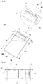
- FIG. 13 is a diagram illustrating a perspective view of a front side of an antenna apparatus, according to the embodiment of the present invention.
- the antenna apparatus of the embodiment is fabricated in accordance with PCB technology.
- An antenna apparatus 500 includes a board body 510, an antenna device 520, a board ground layer 530, an internal matching device 540, and a matching ground layer 550.
- the basic configuration of the antenna apparatus 500 of FIG. 13 is similar to those described above.
- the antenna apparatus 500 further includes a device carrier 560, which has a flat block-like structure with a certain thickness. Additionally, the device carrier 560 is predominantly formed of a dielectric material, which may have different dielectric constant than that of the board body 510. The device carrier 560 is mounted on an upper surface of the board body 510.
- the antenna device 520 is formed on an upper surface of the device carrier 560 through a pattern of metal. Therefore, the antenna device 520 is separated from the board ground layer 530, creating a space therebetween.
- a feed point 521 is disposed at one portion of the antenna device 520 near the board ground layer 530.
- the internal matching device 540 extends from the antenna device 520 and is also formed on the lower surface of the board body 510. The internal matching device 540 may be connected to the antenna device 520 through a matching line 543 elongated along one lateral surface of the device carrier 560, instead of through the matching via.
- the antenna apparatus 500 has a space between the antenna device 520 and the board ground layer 530 that is created by insertion of the device carrier 560. Alternatively, such a space may be created between the internal matching device 540 and the matching ground layer 550. By changing the thickness of the device carrier 560, operation efficiency characteristics of the antenna apparatus 500 may be improved.
- the present invention is not limited thereto.
- the internal matching device and the antenna device may be formed together on the same surface of the board body.
- a related example is described in greater detail below with reference to FIG. 14 .
- FIG. 14 is a diagram illustrating a perspective view of a front side of an antenna apparatus, according to a fifth example, not forming part of the invention but useful for understanding the same.
- the antenna apparatus of this embodiment is fabricated in accordance with PCB technology.
- An antenna apparatus 600 includes a board body 610, an antenna device 620, a board ground layer 630, an internal matching device 640, and a matching ground layer 650.
- the basic configuration of the antenna apparatus 600 of FIG. 14 is similar to those described above.
- the internal matching device 640 together with the antenna device 620, is formed in an upper device region 611 on an upper surface of the board body 610.
- the internal matching device 640 extends from and is located near the antenna device 620.
- the internal matching device 640 is connected to the board ground layer 630 in an upper ground region 613.
- the board body may have a corner-less form or a number of corners other than four.
- the shape of the board body may be determined according to the shape of an internal space for receiving the antenna apparatus in a communication terminal.
- the antenna apparatus may allow for internal impedance matching by specially employing the internal matching device therein.
- the internal matching device is formed as a transmission line, thus reducing a return loss during resonance and improving impedance matching characteristics of the antenna apparatus. Furthermore, the internal matching device, together with the antenna device, resonates in a specific frequency band. Operation efficiency characteristics of the antenna apparatus are also improved.
- a resonance in several or varied frequency bands may be possible.
- the antenna apparatus since impedance matching is allowed without any external matching circuit, the antenna apparatus does not require a space for an external matching circuit. It is therefore possible to realize a space-effective and size-reduced communication terminal.
Landscapes
- Engineering & Computer Science (AREA)
- Computer Networks & Wireless Communication (AREA)
- Details Of Aerials (AREA)
- Waveguide Aerials (AREA)
Description
- The present invention relates generally to an antenna for a wireless communication terminal and, more particularly, to an antenna apparatus allowing for internal impedance matching.
- Wireless communication systems generally provide a variety of multimedia services, which include Global Positioning System (GPS) based services, Bluetooth based services, Internet related services, etc. In order to favorably realize such services, a high data transmission rate is required for a large volume of multimedia data. One way this requirement can be met is by improving the performance of antennas in communication terminals.
- According to
EP 1 936 736 A1 an antenna system with a plurality of radiator elements and feed points connected with a signal processing circuit is provided. - According to
US 2008/0180333 A1 an antenna including a planar dielectric substrate and a conductive ground plane formed on the substrate is provided, wherein a conductive coupling element is formed on the substrate and coupled to the ground plane. - According to
US 2007/0115178 A1 a wide frequency band planar antenna with an elongated portion is provided. - According to
US 2008/0169981 A1 , there is provided an antenna device including a fed partial element, a folded partial element and an open-ended partial element. - Additionally, there is increasing tendency to make communication terminals smaller, thinner, lighter, and more multifunctional, in accordance with market demands for improving mobility and portability of the terminals. Traditional projecting or extractable antennas are often unfavorable for portability and very susceptible to external shock or impact. Therefore, most recently developed antennas are embedded in the terminals. Specifically, the antennas are fabricated in the form of an antenna.
- However, it is difficult to realize a size-reduced antenna apparatus having a reference impedance for resonance in a specific frequency band. Thus, a conventional antenna apparatus in a communication terminal may be coupled to an external matching circuit so as to secure a reference impedance. The use of the external matching circuit may, however, be unfavorable for miniaturization of communication terminals and may cause a return loss during resonance.
- The present invention has been made to address the above problems and/or disadvantages and to provide at least the advantages described below. Accordingly, the present invention provides an antenna apparatus according to the disclosure of independent claim 1 that allows for internal impedance matching. Further embodiments of the invention are shown by the disclosure of the dependent claims.
- Accordingly, an antenna apparatus is provided for internal impedance matching. The antenna apparatus includes a board body formed of a dielectric material and having a flat structure. The apparatus also includes an antenna device extending from a feed point, and having a first impedance. The apparatus further includes an internal matching device disposed on a lower surface of the board body, connected to the antenna device, and having a second impedance used for matching the first impedance with a reference impedance. The antenna device and the internal matching device resonate at the reference impedance in a specific frequency band when a voltage is supplied through the feed point. The antenna device is characterized in that a device carrier having a flat block-like structure with a certain thickness and predominantly formed of a dielectric material is disposed on an upper surface of the board body. Further, the antenna device is disposed on an upper surface of the device carrier and the internal matching device extends from the antenna device to a lateral surface of the device carrier and is connected to the antenna device through a matching line elongated along the lateral surface of the device carrier.
- According to the present invention, the antenna apparatus may allow for internal impedance matching by specially employing the internal matching device therein.
- The internal matching device is formed as a transmission line, thus reducing a return loss during resonance and improving impedance matching characteristics of the antenna apparatus. Furthermore, the internal matching device, together with the antenna device, resonates in a specific frequency band. Operation efficiency characteristics of the antenna apparatus are also improved.
- Additionally, by altering a configuration or a dimension of the internal matching device, a resonance in several or varied frequency bands may be possible.
- Moreover, since impedance matching is allowed without any external matching circuit, the antenna apparatus does not require a space for an external matching circuit. It is therefore possible to realize a space-effective and size-reduced communication terminal.
- The above and other aspects, features and advantages of the present invention will be more apparent from the following detailed description when taken in conjunction with the accompanying drawings, in which:
-
FIG. 1 is a diagram illustrating a perspective view of a front side of an antenna apparatus, according to a first example, not forming part of the invention but useful for understanding the same; -
FIG. 2 is a diagram illustrating a perspective view of a rear side of an antenna apparatus, according to the first example; -
FIG. 3 is a circuit diagram illustrating an equivalent circuit of an antenna apparatus, according to the first example; -
FIG. 4 is a graph illustrating impedance matching characteristics of an antenna apparatus, according to the first example; -
FIG. 5 is a graph illustrating operation efficiency characteristics of an antenna apparatus, according to the first example; -
FIG. 6 is a diagram illustrating a perspective view of a rear side of an antenna apparatus, according to a second example, not forming part of the invention but useful for understanding the same; -
FIG. 7 is a diagram illustrating a perspective view of a rear side of a varied antenna apparatus, according to the second example; -
FIG. 8 is a graph illustrating impedance matching characteristics of a varied antenna apparatus, according to the second example; -
FIG. 9 is a diagram illustrating a perspective view of a rear side of another varied antenna apparatus, according to the second example; -
FIG. 10 is a graph illustrating impedance matching characteristics of another varied antenna apparatus, according to the second example; -
FIG. 11 is a diagram illustrating perspective view of a front side of an antenna apparatus, according to a third example, not forming part of the invention but useful for understanding the same; -
FIG. 12 is a diagram illustrating perspective view of a rear side of an antenna apparatus, according to a fourth example, not forming part of the invention but useful for understanding the same; -
FIG. 13 is a diagram illustrating a perspective view of a front side of an antenna apparatus, according to the embodiment of the present invention; and -
FIG. 14 is a diagram illustrating a perspective view of a front side of an antenna apparatus, according to a fifth example, not forming part of the invention but useful for understanding the same. - Embodiments and Examples of the present invention are described in detail with reference to the accompanying drawings. The same or similar components may be designated by the same or similar reference numerals although they are illustrated in different drawings. Detailed descriptions of constructions or processes known in the art may be omitted to avoid obscuring the subject matter of the present invention.
- Referring initially to
FIG. 1 , a diagram illustrates a perspective view of a front side of anantenna apparatus 100, according to a first example, not forming part of the invention but useful for understanding the same.FIG. 2 is a diagram illustrating a perspective view of a rear side of theantenna apparatus 100, according to the first example. In this example, theantenna apparatus 100 is fabricated in accordance with Printed Circuit Board (PCB) technology. - The
antenna apparatus 100, also referred to as an Internal Matching Antenna (IMA) apparatus, includes aboard body 110, anantenna device 120, aboard ground layer 130, aninternal matching device 140, and a matchingground layer 150. - The
board body 110 is a supporting base of theantenna apparatus 100. Generally, theboard body 110 has a flat structure with at least four corners and the majority of it is formed of a dielectric material. An upper surface of theboard body 110 is divided into anupper device region 111 and anupper ground region 113. Theupper device region 111 may occupy at least two corners of theboard body 110. In addition, a lower surface of theboard body 110 is divided into alower device region 115 and alower ground region 117. Here, thelower device region 115 and thelower ground region 117 may coincide with theupper device region 111 and theupper ground region 113, respectively. - The
antenna device 120 is configured to transmit and receive signals in a predetermined frequency band. Specifically, theantenna device 120 resonates in a specific frequency band and thereby passes signals. Theantenna device 120 is configured to have a first impedance and resonates at a given reference impedance. In addition, theantenna device 120 is formed in theupper device region 111 of theboard body 110 through a pattern of metal on the surface of theupper device region 111. More particularly, theantenna device 120 has afeed point 121 at one end disposed near theboard ground layer 130. Thefeed point 121 may penetrate through theboard body 110 and communicate with the lower surface of theboard body 110. Theantenna device 120 is extended in a particular form from thefeed point 121 on the surface of theupper device region 111. A voltage is supplied to theantenna device 120 through thefeed point 121. - The
antenna device 120 may be composed of at least one parallel component circuit and at least one perpendicular component circuit, which are connected to and distinguished from each other by at least one bent portion. Thefeed point 121 is formed at one end of the perpendicular component circuit of theantenna device 120. For example, theantenna device 120 may be formed as a particular type of transmission line, such as a meander type, a spiral type, a step type, a loop type, and so forth. Also, theantenna device 120 may be embodied in the form of an Inverted L Antenna (ILA). - The
board ground layer 130 is configured for grounding of theantenna device 120. Theboard ground layer 130 is formed in and covers theupper ground region 113 of theboard body 110. - The
internal matching device 140 is configured to match the first impedance of theantenna device 120 with the reference impedance. Therefore, theinternal matching device 140 has a second impedance to match the first impedance with the reference impedance. Theinternal matching device 140, together with theantenna device 120, can resonate at the reference impedance. Specifically, theinternal matching device 140 as well as theantenna device 120 may resonate in a specific frequency band and thereby pass signals. Theinternal matching device 140 is extended from theantenna device 120 and formed in thelower device region 115 of theboard body 110. Theinternal matching device 140 is formed through a pattern of metal, in a manner similar to theantenna device 120. Theinternal matching device 140 has a matching via 141 and amatching line 143. - The matching via 141 is configured to penetrate the
board body 110 from theantenna device 120. Specifically, the matching via 141 is formed as a hole that is filled with conductive material. Therefore, theinternal matching device 140 is physically and electrically connected to theantenna device 120 through the matching via 141. The matching via 141 may be connected to one end of the parallel component circuit of theantenna device 120. Alternative examples may include more than one matching via 141. - The
matching line 143 extends from the matching via 141 and forms a single path on the lower surface of theboard body 110. Thematching line 143 is located in thelower device region 115 and also formed through a pattern of metal. Thematching line 143 may be composed of a first matching line and a second matching line, which are connected to and distinguished from each other by at least one bent portion. The first matching line is extended in a direction that is parallel with the matchingground layer 150, and the second matching line is extended in a direction that is perpendicular to thematching ground layer 150. Additionally, the first matching line may overlap the parallel component circuit of theantenna device 120. For example, thematching line 143 may be formed as a particular type of transmission line, such as a meander type, a spiral type, a step type, a loop type, and so forth. Also, thematching line 143 may be embodied in the corresponding form of ILA. - The matching
ground layer 150 is configured for grounding theinternal matching device 140. Here, the matchingground layer 150 is connected to thematching line 143, specifically at one end of the second matching line. The matchingground layer 150 is formed in and covers thelower ground region 117 of theboard body 110. - In the
antenna apparatus 100, the antenna device and theinternal matching device 140 are designed to have specific electrical properties, which is described in greater detail with respect toFIG. 3. FIG. 3 is a circuit diagram illustrating an equivalent circuit of theantenna apparatus 100, according to the first example. Although this example employs theantenna device 120 and theinternal matching device 140 respectively formed in a single cell, the example is not limited thereto. Alternatively, theantenna device 120 and theinternal matching device 140 may be respectively formed in a plurality of cells. - In the
antenna apparatus 100, theantenna device 120 and theinternal matching device 140 are interconnected. - The
antenna device 120 is configured to have an effective radiation resistance, an effective inductance, and an effective capacitance for allowing resonance in a specific frequency band, and therefore has the first impedance. Specifically, theantenna device 120 is composed of aresistor 123, afirst inductor 125, and afirst capacitor 127. Theresistor 123 and thefirst inductor 125 are connected in series, whereas thefirst inductor 125 and thefirst capacitor 127 are connected in parallel. - The electrical properties of the
antenna device 120 depend upon materials and physical dimensions. For example, the effective radiation resistance of theantenna device 120 may depend on the material (e.g., metal) used in forming theantenna device 120. The effective inductance of theantenna device 120 may depend on a total length and width of theantenna device 120. The effective capacitance of theantenna device 120 may depend on a length of the perpendicular component circuit of theantenna device 120 and a distance between the parallel component circuit and theboard ground layer 130. - The
internal matching device 140 is configured to have a matching capacitance and a matching inductance for matching the first impedance with the reference impedance, and therefore has the second impedance. Specifically, theinternal matching device 140 is composed of asecond capacitor 147 and asecond inductor 149. Thesecond capacitor 147 and thesecond inductor 149 are connected in parallel. - The electrical properties of the
internal matching device 140 depend upon physical dimensions. For example, the matching capacitance of theinternal matching device 140 may depend on an overlapped length and width of theinternal matching device 140 with theantenna device 120. The matching inductance of theinternal matching device 140 may depend on a total length and width of theinternal matching device 140. - The
antenna apparatus 100 with the above configuration has improved characteristics, which are described in greater detail with respect toFIGs. 4 and 5. FIG. 4 is a graph illustrating impedance matching characteristics of theantenna apparatus 100, according to the first example.FIG. 5 is a graph illustrating operation efficiency characteristics of theantenna apparatus 100, according to the first example. Theantenna apparatus 100 having theinternal matching device 140 is represented as IMA, and a conventional antenna apparatus having an external matching circuit is represented as ILA. Experiments were carried out using antenna apparatuses of the same size. - Referring to
FIG. 4 , a difference in impedance matching characteristics between theantenna apparatus 100 and a conventional antenna apparatus was examined by comparing their frequency bandwidths. A Voltage Standing Wave Ratio (VSWR), which indicates a degree of impedance matching, of the frequency bandwidths ranges from 1 to 2. Theantenna apparatus 100 shows a return loss under -6dB in frequencies from about 930MHz to about 1510MHz, which is approximately a 580MHz bandwidth. A conventional antenna apparatus shows a return loss under -6dB in frequencies from about 950MHz to about 1210MHz, which is approximately a 260MHz bandwidth. - Therefore, when compared with a conventional antenna apparatus, the
antenna apparatus 100 allows for impedance matching in wider frequency bandwidth of more than twice that of the conventional apparatus. Specifically, theantenna apparatus 100 can resonate in wider frequency bandwidth when compared with a conventional antenna apparatus. - Referring to
FIG. 5 , a difference in operation efficiency characteristics between theantenna apparatus 100 and a conventional antenna apparatus was examined in the resonant frequencies from about 900MHz to about 1500MHz. As shown, theantenna apparatus 100 has an operation efficiency that is better than that of a conventional antenna apparatus by about 10% or more. - According to this example, the
antenna apparatus 100 allows for internal impedance matching by employing theinternal matching device 140. Theinternal matching device 140 can improve impedance matching characteristics of theantenna apparatus 100. Furthermore, resonance in a specific frequency band of both theinternal matching device 140 and theantenna device 120 can improve operation efficiency characteristics of theantenna apparatus 100. - Although the internal matching device of the aforesaid embodiment has only a single elongated path, the present example is not limited thereto. Alternatively, the internal matching device may have two or more elongated paths. For example, the internal matching device may further include a branch line in addition to the above-described matching line.
-
FIG. 6 is a diagram illustrating a perspective view of a rear side of an antenna apparatus, according to a second example, not forming part of the invention but useful for understanding the same. - Referring to
FIG. 6 , anantenna apparatus 200 includes aboard body 210, anantenna device 220, aboard ground layer 230, aninternal matching device 240, and amatching ground layer 250. Theboard body 210 includes alower device region 215 and alower ground region 217. The basic configuration of theantenna apparatus 200 ofFIG. 6 is similar to that of theantenna apparatus 100 ofFIGs. 1 and2 . - The
internal matching device 240 includes a matching via 241, amatching line 243, and abranch line 245. More particularly, thebranch line 245 diverges and extends from a certain point of thematching line 243, and is located in thelower device region 215 of theboard body 210. As shown inFIG. 6 , thebranch line 245 may extend in a straight line with a first matching line of thematching line 243. Thebranch line 245 may also overlap a parallel component circuit of theantenna device 220. Thebranch line 245, together with thematching line 243, may be formed through a pattern of metal on a surface of thelower device region 215. - The
antenna apparatus 200 having theinternal matching device 240 may resonate in two frequency bands. Specifically, theantenna apparatus 200 allows for impedance matching in a first frequency band and a second frequency band, which is higher than the first frequency band. For example, theantenna apparatus 200 may resonate at about 1GHz and about 2GHz, respectively. -
FIG. 7 is a diagram illustrating a perspective view of a rear side of a varied antenna apparatus, according to the second example.FIG. 8 is a graph illustrating impedance matching characteristics of a varied antenna apparatus, according to the second example. - Referring to
FIG. 7 , a length of amatching line 243a, namely, the length of a path from a matching via 241a to thematching ground layer 250 may be varied. Regardless of abranch line 245a, the second frequency band may vary according to the length of thematching line 243a. Specifically, in anantenna apparatus 200a having aninternal matching device 240a, the second frequency band will increase as thematching line 243a increases in length.FIG. 8 illustrates experimental results of this relationship. -
FIG. 9 is a diagram illustrating a perspective view of a rear side of another varied antenna apparatus, according to the second example.FIG. 10 is a graph illustrating impedance matching characteristics of another varied antenna apparatus, according to the second example. - Referring to
FIG. 9 , a sum of a length of amatching line 243b and a length of abranch line 245b may be varied. Namely, a length of a parallel component circuit from a matching via 241b in aninternal matching device 240b may be varied. The first frequency band may vary according to the sum of the length of thematching line 243b and the length of thebranch line 245b. Specifically, in anantenna apparatus 200b having theinternal matching device 240b, the first frequency band will increase as the sum of the aforesaid lengths decreases.FIG. 10 illustrates experimental results of this relationship. - According to this embodiment of the present invention, the
antenna apparatus branch line internal matching device internal matching device antenna apparatus - Although the above examples describe antenna devices in the form of an ILA, the present invention is not limited thereto. Alternatively, the antenna device of this invention may be formed as one of a particular type of transmission line, such as a meander type, a spiral type, a step type, a loop type, and so forth. Furthermore, the antenna device may be formed as any other type, such as Planar Inverted F Antenna (PIFA), monopole antenna, or dipole antenna. A related case is described in greater detail below with reference to
FIG. 11 . -
FIG. 11 is a diagram illustrating a perspective view of a front side of an antenna apparatus, according to a third examp!e, not forming part of the invention but useful for understanding the same. The antenna apparatus of this example is fabricated in accordance with PCB technology. - An
antenna apparatus board body 310, anantenna device board ground layer 330, aninternal matching device 340, and amatching ground layer 350. The basic configuration of theantenna apparatus FIG. 11 is similar to those described above. - As shown in
FIG. 11(a) , theantenna device 320a is formed as a loop type antenna. Alternatively, as shown inFIG. 11(b) , theantenna device 320b is formed as a PIFA type antenna. Here, theantenna device feed point 321 near theboard ground layer 330 and is connected at other portion to theboard ground layer 330. - Although the above examples describe the internal matching device in the form of an ILA, the present invention is not limited thereto. Similarly, the internal matching device may be alternatively formed as one of a particular type of transmission line, such as a meander type, a spiral type, a step type, a loop type, and so forth. Furthermore, the internal matching device may be formed as any other type, such as Planar Inverted F Antenna (PIFA), monopole antenna, or dipole antenna. A related example is described in greater detail below with reference to
FIG. 12 . -
FIG. 12 is a diagram illustrating a perspective view of a rear side of an antenna apparatus, according to a fourth example, not forming part of the invention but useful for understanding the same. The antenna apparatus of this example is fabricated in accordance with PCB technology. - An
antenna apparatus board body 410, anantenna device 420, aboard ground layer 430, aninternal matching device matching ground layer 450. The basic configuration of theantenna apparatus FIG. 12 is similar to those described above. - As shown in
FIG. 12(a) , theinternal matching device 440a may be formed as a loop type transmission line. Alternatively, as shown inFIG. 12(b) , theinternal matching device 440b may be formed as a meander type transmission line. A matching via 441a or 441b and a first matching line of amatching line antenna device 420. Additionally, a second matching line of thematching line matching ground layer 450. - According to the third and fourth examples in
FIGs. 11(a), 11(b) ,12(a) and 12(c), theantenna apparatus antenna device internal matching device antenna apparatus - Although the above examples describe an antenna device and an internal matching device that are patterned directly on the board body, the present invention is not limited thereto. Alternatively, at least one of the antenna device and the internal matching device may be fabricated on an element other than the board body, such as an external case of a communication terminal, a device carrier mounted on the board body, and so forth. The embodiment of the present invention is described in greater detail below with reference to
FIG. 13 . -
FIG. 13 is a diagram illustrating a perspective view of a front side of an antenna apparatus, according to the embodiment of the present invention. The antenna apparatus of the embodiment is fabricated in accordance with PCB technology. - An antenna apparatus 500 includes a
board body 510, anantenna device 520, aboard ground layer 530, aninternal matching device 540, and amatching ground layer 550. The basic configuration of the antenna apparatus 500 ofFIG. 13 is similar to those described above. - The antenna apparatus 500 further includes a
device carrier 560, which has a flat block-like structure with a certain thickness. Additionally, thedevice carrier 560 is predominantly formed of a dielectric material, which may have different dielectric constant than that of theboard body 510. Thedevice carrier 560 is mounted on an upper surface of theboard body 510. - The
antenna device 520 is formed on an upper surface of thedevice carrier 560 through a pattern of metal. Therefore, theantenna device 520 is separated from theboard ground layer 530, creating a space therebetween. Afeed point 521 is disposed at one portion of theantenna device 520 near theboard ground layer 530. Theinternal matching device 540 extends from theantenna device 520 and is also formed on the lower surface of theboard body 510. Theinternal matching device 540 may be connected to theantenna device 520 through amatching line 543 elongated along one lateral surface of thedevice carrier 560, instead of through the matching via. - The antenna apparatus 500 has a space between the
antenna device 520 and theboard ground layer 530 that is created by insertion of thedevice carrier 560. Alternatively, such a space may be created between theinternal matching device 540 and thematching ground layer 550. By changing the thickness of thedevice carrier 560, operation efficiency characteristics of the antenna apparatus 500 may be improved. - Although the above examples and embodiment describe an internal matching device and an antenna device that are disposed on different surfaces of the board body, the present invention is not limited thereto. Alternatively, the internal matching device and the antenna device may be formed together on the same surface of the board body. A related example is described in greater detail below with reference to
FIG. 14 . -
FIG. 14 is a diagram illustrating a perspective view of a front side of an antenna apparatus, according to a fifth example, not forming part of the invention but useful for understanding the same. The antenna apparatus of this embodiment is fabricated in accordance with PCB technology. - An
antenna apparatus 600 includes aboard body 610, anantenna device 620, aboard ground layer 630, aninternal matching device 640, and a matching ground layer 650. The basic configuration of theantenna apparatus 600 ofFIG. 14 is similar to those described above. - The
internal matching device 640, together with theantenna device 620, is formed in anupper device region 611 on an upper surface of theboard body 610. Theinternal matching device 640 extends from and is located near theantenna device 620. Theinternal matching device 640 is connected to theboard ground layer 630 in anupper ground region 613. - Although the above examples describe the board body as a flat structure with four corners, the present invention is not limited thereto. Alternatively, the board body may have a corner-less form or a number of corners other than four. Specifically, the shape of the board body may be determined according to the shape of an internal space for receiving the antenna apparatus in a communication terminal.
- According to the present invention, the antenna apparatus may allow for internal impedance matching by specially employing the internal matching device therein.
- The internal matching device is formed as a transmission line, thus reducing a return loss during resonance and improving impedance matching characteristics of the antenna apparatus. Furthermore, the internal matching device, together with the antenna device, resonates in a specific frequency band. Operation efficiency characteristics of the antenna apparatus are also improved.
- Additionally, by altering a configuration or a dimension of the internal matching device, a resonance in several or varied frequency bands may be possible.
- Moreover, since impedance matching is allowed without any external matching circuit, the antenna apparatus does not require a space for an external matching circuit. It is therefore possible to realize a space-effective and size-reduced communication terminal.
Claims (5)
- An antenna apparatus (500) for internal impedance matching, the antenna apparatus comprising:a board body (510) formed of a dielectric material and having a flat structure;an antenna device (520) extending from a feed point, and having a first impedance; andan internal matching device (540) disposed on a lower surface of the board body, connected to the antenna device, and having a second impedance used for matching the first impedance with a reference impedance,wherein the antenna device and the internal matching device resonate at the reference impedance in a specific frequency band when a voltage is supplied through the feed point;characterized in thata device carrier (560) having a flat block-like structure with a certain thickness and predominantly formed of a dielectric material is disposed on an upper surface of the board body;the antenna device (520) is disposed on an upper surface of the device carrier (560), andthe internal matching device (540) extends from the antenna device to a lateral surface of the device carrier (560) and is connected to the antenna device (520) through a matching line (543) elongated along the lateral surface of the device carrier (560).
- The antenna apparatus of claim 1, wherein the matching line (543) forms a single path.
- The antenna apparatus of claim 1, wherein the internal matching device (540) further comprises a branch line that diverges and extends from the matching line (543).
- The antenna apparatus of claim 1, wherein the antenna device (520) and the internal matching device (540) are formed through patterns on the board body (510) and the device carrier (560).
- The antenna apparatus of claim 1, further comprising
a matching ground layer (550) disposed on the lower surface of the board body (510) and connected to the internal matching device (540).
Applications Claiming Priority (2)
| Application Number | Priority Date | Filing Date | Title |
|---|---|---|---|
| KR1020080132997A KR101535641B1 (en) | 2008-12-24 | 2008-12-24 | Antenna device for internal impedance matching |
| PCT/KR2009/007793 WO2010074538A2 (en) | 2008-12-24 | 2009-12-24 | Antenna apparatus for internal impedance matching |
Publications (3)
| Publication Number | Publication Date |
|---|---|
| EP2377197A2 EP2377197A2 (en) | 2011-10-19 |
| EP2377197A4 EP2377197A4 (en) | 2014-04-30 |
| EP2377197B1 true EP2377197B1 (en) | 2020-04-29 |
Family
ID=42265245
Family Applications (1)
| Application Number | Title | Priority Date | Filing Date |
|---|---|---|---|
| EP09835304.8A Active EP2377197B1 (en) | 2008-12-24 | 2009-12-24 | Antenna apparatus for internal impedance matching |
Country Status (4)
| Country | Link |
|---|---|
| US (1) | US8284116B2 (en) |
| EP (1) | EP2377197B1 (en) |
| KR (1) | KR101535641B1 (en) |
| WO (1) | WO2010074538A2 (en) |
Families Citing this family (5)
| Publication number | Priority date | Publication date | Assignee | Title |
|---|---|---|---|---|
| KR101919840B1 (en) | 2012-07-10 | 2018-11-19 | 삼성전자주식회사 | Broad band tunable antenna device for portable terminal |
| US9124003B2 (en) * | 2013-02-21 | 2015-09-01 | Qualcomm Incorporated | Multiple antenna system |
| KR20190129487A (en) | 2018-05-11 | 2019-11-20 | 주식회사 슈피겐코리아 | Wireless charging trasmitter with automatic recharging |
| US11063345B2 (en) * | 2018-07-17 | 2021-07-13 | Mastodon Design Llc | Systems and methods for providing a wearable antenna |
| CN112467369A (en) * | 2020-11-18 | 2021-03-09 | 上海磐启微电子有限公司 | WIFI board carries antenna |
Family Cites Families (11)
| Publication number | Priority date | Publication date | Assignee | Title |
|---|---|---|---|---|
| US4079268A (en) * | 1976-10-06 | 1978-03-14 | Nasa | Thin conformal antenna array for microwave power conversion |
| KR100363303B1 (en) * | 1999-06-19 | 2002-11-30 | 우종명 | Printing-Type Inverted F Antenna |
| CN101069322B (en) * | 2004-12-02 | 2011-07-20 | 皇家飞利浦电子股份有限公司 | Mobile phones with built-in flat-screen television antennas suitable for suppressing radiotelephone signals |
| US7253772B2 (en) * | 2005-11-24 | 2007-08-07 | Delta Networks, Inc. | Wide frequency band planar antenna |
| CN101385202A (en) * | 2005-12-14 | 2009-03-11 | 堪萨斯州立大学 | Microstrip antenna for rfid device |
| TWI329384B (en) * | 2006-08-18 | 2010-08-21 | Hon Hai Prec Ind Co Ltd | Planar antenna device |
| EP2095464A4 (en) * | 2006-11-16 | 2012-10-24 | Galtronics Ltd | Compact antenna |
| KR100842071B1 (en) * | 2006-12-18 | 2008-06-30 | 삼성전자주식회사 | Concurrent mode antenna system |
| FR2910182A1 (en) | 2006-12-18 | 2008-06-20 | Thomson Licensing Sas | IMPROVEMENT OF PLANAR ANTENNAS WITH RADIANT SLOT |
| JP4864733B2 (en) | 2007-01-16 | 2012-02-01 | 株式会社東芝 | Antenna device |
| CN201498592U (en) * | 2009-08-06 | 2010-06-02 | 国基电子(上海)有限公司 | dual frequency antenna |
-
2008
- 2008-12-24 KR KR1020080132997A patent/KR101535641B1/en active Active
-
2009
- 2009-12-24 WO PCT/KR2009/007793 patent/WO2010074538A2/en not_active Ceased
- 2009-12-24 US US12/647,128 patent/US8284116B2/en active Active
- 2009-12-24 EP EP09835304.8A patent/EP2377197B1/en active Active
Non-Patent Citations (1)
| Title |
|---|
| None * |
Also Published As
| Publication number | Publication date |
|---|---|
| US20100156748A1 (en) | 2010-06-24 |
| KR20100074532A (en) | 2010-07-02 |
| EP2377197A4 (en) | 2014-04-30 |
| EP2377197A2 (en) | 2011-10-19 |
| WO2010074538A2 (en) | 2010-07-01 |
| KR101535641B1 (en) | 2015-07-10 |
| WO2010074538A3 (en) | 2010-09-23 |
| US8284116B2 (en) | 2012-10-09 |
Similar Documents
| Publication | Publication Date | Title |
|---|---|---|
| CN103155281B (en) | For cell phone and other loop antennas applied | |
| US6980154B2 (en) | Planar inverted F antennas including current nulls between feed and ground couplings and related communications devices | |
| US7663551B2 (en) | Multiband antenna apparatus and methods | |
| KR100856310B1 (en) | Mobile-communication terminal | |
| TWI587575B (en) | Antenna isolation technique using a tuned ground plane notch | |
| US7193565B2 (en) | Meanderline coupled quadband antenna for wireless handsets | |
| US20080204328A1 (en) | Dual antenna apparatus and methods | |
| US8207895B2 (en) | Shorted monopole antenna | |
| US8643549B2 (en) | Multi-resonant antenna | |
| US9142884B2 (en) | Antenna device | |
| CN102812593A (en) | Dielectric Chip Antenna | |
| CN110770975B (en) | Antenna arrangement and device comprising such an antenna arrangement | |
| US8284116B2 (en) | Antenna apparatus for internal impedance matching | |
| CN103460505B (en) | Make ground connection radiant body and the grounded antenna of electricity container | |
| WO2010139120A1 (en) | Multi-band monopole antennas with parasitic elements | |
| EP2204880B1 (en) | Single band antenna and antenna module | |
| KR20080016353A (en) | Multiband antenna | |
| US9124352B2 (en) | Data communication terminal apparatus | |
| WO2007077461A1 (en) | Laptop computer antenna device | |
| CN2901607Y (en) | Small double frequency MLA built-in antenna for cell phone | |
| HK1235918B (en) | A loop antenna for mobile handset and other applications | |
| HK1235918A1 (en) | A loop antenna for mobile handset and other applications | |
| HK1235918A (en) | A loop antenna for mobile handset and other applications | |
| TWM288013U (en) | Micro GPS chip antenna at 1575MHz suitable for operation of handheld communication equipment |
Legal Events
| Date | Code | Title | Description |
|---|---|---|---|
| PUAI | Public reference made under article 153(3) epc to a published international application that has entered the european phase |
Free format text: ORIGINAL CODE: 0009012 |
|
| 17P | Request for examination filed |
Effective date: 20110624 |
|
| AK | Designated contracting states |
Kind code of ref document: A2 Designated state(s): AT BE BG CH CY CZ DE DK EE ES FI FR GB GR HR HU IE IS IT LI LT LU LV MC MK MT NL NO PL PT RO SE SI SK SM TR |
|
| DAX | Request for extension of the european patent (deleted) | ||
| RAP1 | Party data changed (applicant data changed or rights of an application transferred) |
Owner name: SAMSUNG ELECTRONICS CO., LTD. |
|
| A4 | Supplementary search report drawn up and despatched |
Effective date: 20140402 |
|
| RIC1 | Information provided on ipc code assigned before grant |
Ipc: H01Q 9/42 20060101ALI20140327BHEP Ipc: H01Q 1/38 20060101AFI20140327BHEP Ipc: H01Q 1/24 20060101ALI20140327BHEP |
|
| STAA | Information on the status of an ep patent application or granted ep patent |
Free format text: STATUS: EXAMINATION IS IN PROGRESS |
|
| 17Q | First examination report despatched |
Effective date: 20170327 |
|
| GRAP | Despatch of communication of intention to grant a patent |
Free format text: ORIGINAL CODE: EPIDOSNIGR1 |
|
| STAA | Information on the status of an ep patent application or granted ep patent |
Free format text: STATUS: GRANT OF PATENT IS INTENDED |
|
| INTG | Intention to grant announced |
Effective date: 20191118 |
|
| GRAS | Grant fee paid |
Free format text: ORIGINAL CODE: EPIDOSNIGR3 |
|
| GRAA | (expected) grant |
Free format text: ORIGINAL CODE: 0009210 |
|
| STAA | Information on the status of an ep patent application or granted ep patent |
Free format text: STATUS: THE PATENT HAS BEEN GRANTED |
|
| AK | Designated contracting states |
Kind code of ref document: B1 Designated state(s): AT BE BG CH CY CZ DE DK EE ES FI FR GB GR HR HU IE IS IT LI LT LU LV MC MK MT NL NO PL PT RO SE SI SK SM TR |
|
| REG | Reference to a national code |
Ref country code: GB Ref legal event code: FG4D |
|
| REG | Reference to a national code |
Ref country code: CH Ref legal event code: EP |
|
| REG | Reference to a national code |
Ref country code: AT Ref legal event code: REF Ref document number: 1264690 Country of ref document: AT Kind code of ref document: T Effective date: 20200515 |
|
| REG | Reference to a national code |
Ref country code: DE Ref legal event code: R096 Ref document number: 602009061912 Country of ref document: DE |
|
| REG | Reference to a national code |
Ref country code: IE Ref legal event code: FG4D |
|
| REG | Reference to a national code |
Ref country code: NL Ref legal event code: FP |
|
| REG | Reference to a national code |
Ref country code: LT Ref legal event code: MG4D |
|
| PG25 | Lapsed in a contracting state [announced via postgrant information from national office to epo] |
Ref country code: GR Free format text: LAPSE BECAUSE OF FAILURE TO SUBMIT A TRANSLATION OF THE DESCRIPTION OR TO PAY THE FEE WITHIN THE PRESCRIBED TIME-LIMIT Effective date: 20200730 Ref country code: SE Free format text: LAPSE BECAUSE OF FAILURE TO SUBMIT A TRANSLATION OF THE DESCRIPTION OR TO PAY THE FEE WITHIN THE PRESCRIBED TIME-LIMIT Effective date: 20200429 Ref country code: LT Free format text: LAPSE BECAUSE OF FAILURE TO SUBMIT A TRANSLATION OF THE DESCRIPTION OR TO PAY THE FEE WITHIN THE PRESCRIBED TIME-LIMIT Effective date: 20200429 Ref country code: PT Free format text: LAPSE BECAUSE OF FAILURE TO SUBMIT A TRANSLATION OF THE DESCRIPTION OR TO PAY THE FEE WITHIN THE PRESCRIBED TIME-LIMIT Effective date: 20200831 Ref country code: IS Free format text: LAPSE BECAUSE OF FAILURE TO SUBMIT A TRANSLATION OF THE DESCRIPTION OR TO PAY THE FEE WITHIN THE PRESCRIBED TIME-LIMIT Effective date: 20200829 Ref country code: NO Free format text: LAPSE BECAUSE OF FAILURE TO SUBMIT A TRANSLATION OF THE DESCRIPTION OR TO PAY THE FEE WITHIN THE PRESCRIBED TIME-LIMIT Effective date: 20200729 Ref country code: FI Free format text: LAPSE BECAUSE OF FAILURE TO SUBMIT A TRANSLATION OF THE DESCRIPTION OR TO PAY THE FEE WITHIN THE PRESCRIBED TIME-LIMIT Effective date: 20200429 |
|
| REG | Reference to a national code |
Ref country code: AT Ref legal event code: MK05 Ref document number: 1264690 Country of ref document: AT Kind code of ref document: T Effective date: 20200429 |
|
| PG25 | Lapsed in a contracting state [announced via postgrant information from national office to epo] |
Ref country code: BG Free format text: LAPSE BECAUSE OF FAILURE TO SUBMIT A TRANSLATION OF THE DESCRIPTION OR TO PAY THE FEE WITHIN THE PRESCRIBED TIME-LIMIT Effective date: 20200729 Ref country code: HR Free format text: LAPSE BECAUSE OF FAILURE TO SUBMIT A TRANSLATION OF THE DESCRIPTION OR TO PAY THE FEE WITHIN THE PRESCRIBED TIME-LIMIT Effective date: 20200429 Ref country code: LV Free format text: LAPSE BECAUSE OF FAILURE TO SUBMIT A TRANSLATION OF THE DESCRIPTION OR TO PAY THE FEE WITHIN THE PRESCRIBED TIME-LIMIT Effective date: 20200429 |
|
| PG25 | Lapsed in a contracting state [announced via postgrant information from national office to epo] |
Ref country code: EE Free format text: LAPSE BECAUSE OF FAILURE TO SUBMIT A TRANSLATION OF THE DESCRIPTION OR TO PAY THE FEE WITHIN THE PRESCRIBED TIME-LIMIT Effective date: 20200429 Ref country code: AT Free format text: LAPSE BECAUSE OF FAILURE TO SUBMIT A TRANSLATION OF THE DESCRIPTION OR TO PAY THE FEE WITHIN THE PRESCRIBED TIME-LIMIT Effective date: 20200429 Ref country code: SM Free format text: LAPSE BECAUSE OF FAILURE TO SUBMIT A TRANSLATION OF THE DESCRIPTION OR TO PAY THE FEE WITHIN THE PRESCRIBED TIME-LIMIT Effective date: 20200429 Ref country code: IT Free format text: LAPSE BECAUSE OF FAILURE TO SUBMIT A TRANSLATION OF THE DESCRIPTION OR TO PAY THE FEE WITHIN THE PRESCRIBED TIME-LIMIT Effective date: 20200429 Ref country code: DK Free format text: LAPSE BECAUSE OF FAILURE TO SUBMIT A TRANSLATION OF THE DESCRIPTION OR TO PAY THE FEE WITHIN THE PRESCRIBED TIME-LIMIT Effective date: 20200429 Ref country code: CZ Free format text: LAPSE BECAUSE OF FAILURE TO SUBMIT A TRANSLATION OF THE DESCRIPTION OR TO PAY THE FEE WITHIN THE PRESCRIBED TIME-LIMIT Effective date: 20200429 Ref country code: RO Free format text: LAPSE BECAUSE OF FAILURE TO SUBMIT A TRANSLATION OF THE DESCRIPTION OR TO PAY THE FEE WITHIN THE PRESCRIBED TIME-LIMIT Effective date: 20200429 Ref country code: ES Free format text: LAPSE BECAUSE OF FAILURE TO SUBMIT A TRANSLATION OF THE DESCRIPTION OR TO PAY THE FEE WITHIN THE PRESCRIBED TIME-LIMIT Effective date: 20200429 |
|
| REG | Reference to a national code |
Ref country code: DE Ref legal event code: R097 Ref document number: 602009061912 Country of ref document: DE |
|
| PG25 | Lapsed in a contracting state [announced via postgrant information from national office to epo] |
Ref country code: SK Free format text: LAPSE BECAUSE OF FAILURE TO SUBMIT A TRANSLATION OF THE DESCRIPTION OR TO PAY THE FEE WITHIN THE PRESCRIBED TIME-LIMIT Effective date: 20200429 Ref country code: PL Free format text: LAPSE BECAUSE OF FAILURE TO SUBMIT A TRANSLATION OF THE DESCRIPTION OR TO PAY THE FEE WITHIN THE PRESCRIBED TIME-LIMIT Effective date: 20200429 |
|
| PLBE | No opposition filed within time limit |
Free format text: ORIGINAL CODE: 0009261 |
|
| STAA | Information on the status of an ep patent application or granted ep patent |
Free format text: STATUS: NO OPPOSITION FILED WITHIN TIME LIMIT |
|
| 26N | No opposition filed |
Effective date: 20210201 |
|
| PG25 | Lapsed in a contracting state [announced via postgrant information from national office to epo] |
Ref country code: SI Free format text: LAPSE BECAUSE OF FAILURE TO SUBMIT A TRANSLATION OF THE DESCRIPTION OR TO PAY THE FEE WITHIN THE PRESCRIBED TIME-LIMIT Effective date: 20200429 |
|
| REG | Reference to a national code |
Ref country code: CH Ref legal event code: PL |
|
| PG25 | Lapsed in a contracting state [announced via postgrant information from national office to epo] |
Ref country code: MC Free format text: LAPSE BECAUSE OF FAILURE TO SUBMIT A TRANSLATION OF THE DESCRIPTION OR TO PAY THE FEE WITHIN THE PRESCRIBED TIME-LIMIT Effective date: 20200429 |
|
| REG | Reference to a national code |
Ref country code: BE Ref legal event code: MM Effective date: 20201231 |
|
| PG25 | Lapsed in a contracting state [announced via postgrant information from national office to epo] |
Ref country code: IE Free format text: LAPSE BECAUSE OF NON-PAYMENT OF DUE FEES Effective date: 20201224 Ref country code: FR Free format text: LAPSE BECAUSE OF NON-PAYMENT OF DUE FEES Effective date: 20201231 Ref country code: LU Free format text: LAPSE BECAUSE OF NON-PAYMENT OF DUE FEES Effective date: 20201224 |
|
| PG25 | Lapsed in a contracting state [announced via postgrant information from national office to epo] |
Ref country code: LI Free format text: LAPSE BECAUSE OF NON-PAYMENT OF DUE FEES Effective date: 20201231 Ref country code: CH Free format text: LAPSE BECAUSE OF NON-PAYMENT OF DUE FEES Effective date: 20201231 |
|
| PG25 | Lapsed in a contracting state [announced via postgrant information from national office to epo] |
Ref country code: TR Free format text: LAPSE BECAUSE OF FAILURE TO SUBMIT A TRANSLATION OF THE DESCRIPTION OR TO PAY THE FEE WITHIN THE PRESCRIBED TIME-LIMIT Effective date: 20200429 Ref country code: MT Free format text: LAPSE BECAUSE OF FAILURE TO SUBMIT A TRANSLATION OF THE DESCRIPTION OR TO PAY THE FEE WITHIN THE PRESCRIBED TIME-LIMIT Effective date: 20200429 Ref country code: CY Free format text: LAPSE BECAUSE OF FAILURE TO SUBMIT A TRANSLATION OF THE DESCRIPTION OR TO PAY THE FEE WITHIN THE PRESCRIBED TIME-LIMIT Effective date: 20200429 |
|
| PG25 | Lapsed in a contracting state [announced via postgrant information from national office to epo] |
Ref country code: MK Free format text: LAPSE BECAUSE OF FAILURE TO SUBMIT A TRANSLATION OF THE DESCRIPTION OR TO PAY THE FEE WITHIN THE PRESCRIBED TIME-LIMIT Effective date: 20200429 |
|
| PG25 | Lapsed in a contracting state [announced via postgrant information from national office to epo] |
Ref country code: BE Free format text: LAPSE BECAUSE OF NON-PAYMENT OF DUE FEES Effective date: 20201231 |
|
| PGFP | Annual fee paid to national office [announced via postgrant information from national office to epo] |
Ref country code: NL Payment date: 20251120 Year of fee payment: 17 |
|
| PGFP | Annual fee paid to national office [announced via postgrant information from national office to epo] |
Ref country code: DE Payment date: 20251120 Year of fee payment: 17 |
|
| PGFP | Annual fee paid to national office [announced via postgrant information from national office to epo] |
Ref country code: GB Payment date: 20251120 Year of fee payment: 17 |