EP2375570A2 - Power switches for aircraft - Google Patents
Power switches for aircraft Download PDFInfo
- Publication number
- EP2375570A2 EP2375570A2 EP11161543A EP11161543A EP2375570A2 EP 2375570 A2 EP2375570 A2 EP 2375570A2 EP 11161543 A EP11161543 A EP 11161543A EP 11161543 A EP11161543 A EP 11161543A EP 2375570 A2 EP2375570 A2 EP 2375570A2
- Authority
- EP
- European Patent Office
- Prior art keywords
- power switch
- solid state
- state power
- integrated solid
- integrated
- Prior art date
- Legal status (The legal status is an assumption and is not a legal conclusion. Google has not performed a legal analysis and makes no representation as to the accuracy of the status listed.)
- Withdrawn
Links
- 239000000463 material Substances 0.000 claims abstract description 39
- 239000007787 solid Substances 0.000 claims abstract description 39
- 238000000034 method Methods 0.000 claims abstract description 13
- 238000009826 distribution Methods 0.000 claims abstract description 10
- 239000004065 semiconductor Substances 0.000 claims abstract description 9
- 230000005669 field effect Effects 0.000 claims abstract description 7
- 238000004519 manufacturing process Methods 0.000 claims abstract description 5
- 239000000758 substrate Substances 0.000 claims description 18
- 229910052710 silicon Inorganic materials 0.000 claims description 15
- 239000010703 silicon Substances 0.000 claims description 15
- 238000001816 cooling Methods 0.000 abstract description 8
- XUIMIQQOPSSXEZ-UHFFFAOYSA-N Silicon Chemical compound [Si] XUIMIQQOPSSXEZ-UHFFFAOYSA-N 0.000 description 12
- 238000005229 chemical vapour deposition Methods 0.000 description 2
- 238000010276 construction Methods 0.000 description 2
- 238000005516 engineering process Methods 0.000 description 2
- 230000008569 process Effects 0.000 description 2
- 230000004044 response Effects 0.000 description 2
- 239000002210 silicon-based material Substances 0.000 description 2
- 230000003068 static effect Effects 0.000 description 2
- JBRZTFJDHDCESZ-UHFFFAOYSA-N AsGa Chemical compound [As]#[Ga] JBRZTFJDHDCESZ-UHFFFAOYSA-N 0.000 description 1
- JMASRVWKEDWRBT-UHFFFAOYSA-N Gallium nitride Chemical compound [Ga]#N JMASRVWKEDWRBT-UHFFFAOYSA-N 0.000 description 1
- 230000009471 action Effects 0.000 description 1
- 230000009977 dual effect Effects 0.000 description 1
- 239000012530 fluid Substances 0.000 description 1
- 238000010438 heat treatment Methods 0.000 description 1
- 238000012423 maintenance Methods 0.000 description 1
- 238000001451 molecular beam epitaxy Methods 0.000 description 1
- HBMJWWWQQXIZIP-UHFFFAOYSA-N silicon carbide Chemical compound [Si+]#[C-] HBMJWWWQQXIZIP-UHFFFAOYSA-N 0.000 description 1
- 230000001052 transient effect Effects 0.000 description 1
Images


Classifications
-
- H—ELECTRICITY
- H10—SEMICONDUCTOR DEVICES; ELECTRIC SOLID-STATE DEVICES NOT OTHERWISE PROVIDED FOR
- H10D—INORGANIC ELECTRIC SEMICONDUCTOR DEVICES
- H10D62/00—Semiconductor bodies, or regions thereof, of devices having potential barriers
- H10D62/10—Shapes, relative sizes or dispositions of the regions of the semiconductor bodies; Shapes of the semiconductor bodies
- H10D62/124—Shapes, relative sizes or dispositions of the regions of semiconductor bodies or of junctions between the regions
-
- H—ELECTRICITY
- H03—ELECTRONIC CIRCUITRY
- H03K—PULSE TECHNIQUE
- H03K17/00—Electronic switching or gating, i.e. not by contact-making and –breaking
- H03K17/08—Modifications for protecting switching circuit against overcurrent or overvoltage
- H03K17/082—Modifications for protecting switching circuit against overcurrent or overvoltage by feedback from the output to the control circuit
-
- H—ELECTRICITY
- H10—SEMICONDUCTOR DEVICES; ELECTRIC SOLID-STATE DEVICES NOT OTHERWISE PROVIDED FOR
- H10D—INORGANIC ELECTRIC SEMICONDUCTOR DEVICES
- H10D12/00—Bipolar devices controlled by the field effect, e.g. insulated-gate bipolar transistors [IGBT]
- H10D12/411—Insulated-gate bipolar transistors [IGBT]
- H10D12/441—Vertical IGBTs
-
- H—ELECTRICITY
- H10—SEMICONDUCTOR DEVICES; ELECTRIC SOLID-STATE DEVICES NOT OTHERWISE PROVIDED FOR
- H10D—INORGANIC ELECTRIC SEMICONDUCTOR DEVICES
- H10D30/00—Field-effect transistors [FET]
- H10D30/60—Insulated-gate field-effect transistors [IGFET]
- H10D30/64—Double-diffused metal-oxide semiconductor [DMOS] FETs
- H10D30/66—Vertical DMOS [VDMOS] FETs
-
- H—ELECTRICITY
- H10—SEMICONDUCTOR DEVICES; ELECTRIC SOLID-STATE DEVICES NOT OTHERWISE PROVIDED FOR
- H10D—INORGANIC ELECTRIC SEMICONDUCTOR DEVICES
- H10D62/00—Semiconductor bodies, or regions thereof, of devices having potential barriers
- H10D62/10—Shapes, relative sizes or dispositions of the regions of the semiconductor bodies; Shapes of the semiconductor bodies
- H10D62/13—Semiconductor regions connected to electrodes carrying current to be rectified, amplified or switched, e.g. source or drain regions
- H10D62/149—Source or drain regions of field-effect devices
- H10D62/151—Source or drain regions of field-effect devices of IGFETs
- H10D62/156—Drain regions of DMOS transistors
Definitions
- the present invention relates generally to power switches for aircraft.
- the present invention relates to improved power switching devices and methods for aircraft which provide fault protection for aircraft power distribution wiring.
- Aircraft power distribution systems are safety critical. Hence they need to be protected from over-current conditions that may be caused, for example, by lightning strikes, short circuits, etc., that might otherwise produce high currents that permanently damage or break wiring or other electrical components.
- Over-current protection is often provided by using various devices and systems that trip and break a circuit if a detected current (I fault ) is larger than a maximum operating or rated current (I normal ) in, for example, an aircraft wiring harness.
- SSPCs Solid State Power Controllers
- MOSFETs metal-oxide-silicon field effect transistors
- MOSFET-based systems have various advantages, they also operate at a relatively high temperature (e.g. the MOSFET junction temperature may typically be ⁇ 100 °C). Because of this, there is only a relatively small temperature range (i.e. a window of about 50-60 °C) in which the MOSFET devices need to be turned off in the event of a fault in order to prevent them heating into a temperature range above which silicon stops behaving as a semiconductor (i.e. above about 165 °C).
- MOSFETs are often provided with passive and/or active cooling.
- forced fluid cooling may be used, as may the provision of one or more heatsink devices.
- the system may also be formed using many individual MOSFET devices provided in parallel, and/or by using very bulky power devices, in order to provide a large physical amount of semiconductor material that can dissipate any heat generated under fault conditions without provoking a substantial temperature rise in the MOSFETs (essentially by reducing the value of R ).
- MOSFET-based power protection systems are generally fairly bulky and heavy. Clearly, this is disadvantageous, particularly in aircraft.
- an integrated solid state power switch for fault protection in an aircraft power distribution system.
- the integrated solid state power switch is formed of semiconductor material which provides a field effect transistor (FET) channel that is operable during normal device operation to provide an operating current flow path and a bipolar transistor channel that is operable during device overload conditions to provide an overload current flow path.
- FET field effect transistor
- bipolar transistor that is operable during device overload conditions to provide an overload current flow path.
- substantially all of a trip/overload current is routed through the overload current flow path to provide surge current protection.
- the switch may be a switch according to an embodiment of the aforementioned first aspect of the present invention.
- the method comprises providing a substrate layer, doping the substrate layer to provide at least one MOSFET drain region and at least one IGBT collector region, providing a channel layer over the substrate layer, forming at least one contact in the channel layer, and forming at least one gate contact over the contact(s).
- various embodiments of the present invention are able automatically to provide over-current protection by virtue of their inherent device physics, without the need for external sensors or active device control. Additionally, as the inherent device structure may provide separate operating current flow and overload current flow paths in the same integrated device, compact low-weight high current devices can be provided whilst eliminating or substantially reducing the need to provide heavy, expensive, or possibly unreliable, forced or unforced cooling devices.
- Figure 1 shows a vertically integrated power switch 200 in accordance with a first embodiment of the present invention.
- the vertically integrated solid state power switch 200 is particularly suited for use in fault protection of aircraft power distribution systems as it is light-weight, compact, reliable and does not require the use of forced cooling to maintain device operational integrity.
- the vertically integrated solid state power switch 200 is formed from silicon material 250.
- the vertically integrated solid state power switch 200 is made from a single high purity silicon wafer 204.
- the silicon wafer 204 is doped on one side to provide a central N + -type MOSFET drain region 212.
- P-type IGBT doped collector regions 208, 210 are provided concentrically surrounding the N + -type MOSFET drain region 212 within a substrate layer 202.
- the substrate layer 202 is provided with contacts (not shown) and forms a combined drain/collector of the vertically integrated solid state power switch 200.
- a channel layer 214 is provided in the silicon wafer 204.
- the channel layer is doped N - -type and is provided adjacent to the substrate layer 202.
- the channel layer 214 is electrically connected to the substrate layer 202 and to a source/emitter connection of the vertically integrated solid state power switch 200. In operation, the channel layer 214 provides both an operating current flow path 242 and an overload current flow path 240.
- an electrical contact 220 is formed on the opposite face of the wafer 204 from the substrate layer 202.
- the contact 220 is generally ring-shaped and concentrically aligned with the centre of the drain region 212.
- the contact 220 comprises a radially-outermost N + -type ring of material 216, 218 doped into the wafer 204 and exposed at the opposite face of the wafer 204.
- a radially-innermost concentric P-type ring of material 221, 222 is doped into the wafer 204 and is in contact with the channel layer 214, the opposite face of the wafer 204 and the outermost ring of material 216, 218.
- a third concentric ring of N - -type material 224, 226 is provided in contact with the opposite face of the wafer 204, the outermost ring of material 216, 218 and the innermost ring of material 221, 222 to complete the structure of the contact 220.
- the channel layer 214 extends from the substrate layer 202 to the surface of the opposite face of the wafer 204 through the centre of the innermost ring of material 221, 222. Above this surface-exposed channel layer 214 a disc-shaped layer of oxide material 228 is provided. The oxide material 228 also overlaps the innermost ring of material 221, 222 and part of the third ring of material 224, 226 where they are exposed at the surface of the opposite face of the wafer 204. A metallic layer of material 230 is formed over the oxide material 228 and together these provide a gate contact 206 for the vertically integrated power switch 200.
- the design of the vertically integrated power switch 200 is advantageous in that the MOSFET structure and IGBT structure occupy substantially same volume vertically between the substrate layer 202 and the gate contact 206 so that a relatively compact device is provided that requires a minimal amount of wafer space and thus also of semiconductor material. This provides advantages in terms of size, weight and cost.
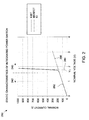
- FIG. 2 shows a graph 280 illustrating static V-I characteristics of the vertically integrated power switch 200 of Figure 1 . Operation of the vertically integrated power switch 200 will now be described in connection with the graph 280.
- a field effect transistor (FET) channel provides an operating current flow path 242 in which current flows from the source/emitter contact to the drain contact and which can be modulated by a voltage applied to the gate contact 206.
- the voltage drop between source/emitter and drain V initially increases linearly whilst the current follows the operating current flow path 242.
- This is illustrated in Figure 2 by the initial straight line portion of the integrated device (ID) V-I current profile 282, and shows that the vertically integrated power switch 200 has a substantially constant resistance R at relatively low operating currents.
- the V-I characteristics of the vertically integrated power switch 200 are thus initially dominated by the FET channel substantially following the MOSFET current profile 286.
- the voltage drop V becomes sufficient to cause conduction to begin across a band gap region formed between the P-type collector regions 208, 210 and the N - -type channel material of channel layer 214.
- This p-n junction region forms a bipolar transistor channel in an IGBT structure formed by the contact 220, the channel layer 214 and the collector regions 208, 210.
- the source/emitter-drain/collector voltage drop increases above a threshold value V T and the IGBT current profile 284 of the bipolar transistor channel begins to dominate the current profile 282, the bipolar transistor channel thereby providing the overload current flow path 240.
- R for a conventional MOSFET device experiencing fault current conditions. This helps reduce the cooling requirements and also means compact devices can be used.
- the inherent electrical characteristics of the vertically integrated power switch 200 provide the current profile 282 and thereby enable automatic switching of current from the operating current flow path 242 to the overload current path 240 should the vertically integrated power switch 200 experience current and/or voltage overload conditions.
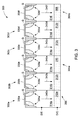
- FIG. 3 shows a horizontally integrated power switch 300 in accordance with an embodiment of the present invention.
- the horizontally integrated solid state power switch 300 is formed from silicon material 350.
- the horizontally integrated solid state power switch 300 is made from a single high purity silicon wafer, although other materials such as gallium arsenide (GaAs), gallium nitride (GaN), silicon carbide (SiC), etc., may additionally, or alternatively, be used.
- GaAs gallium arsenide
- GaN gallium nitride
- SiC silicon carbide
- the horizontally integrated solid state power switch 300 includes a plurality of adjacently positioned MOSFET devices 302a, 302b, 302c, 302d and a plurality of spaced IGBT devices 304a, 304b.
- two adjacent MOSFET devices 302a, 302b, 302c, 302d are provided for every IGBT device 304a, 304b in an alternating regularly spaced pattern with respective pairs of MOSFETs 302a, 302b, 302c, 302d separating the IGBT devices 304a, 304b.
- a ratio ( ⁇ ) of the number MOSFET structures (m) to the number of IGBT structures ( i ) is greater than 1:1.
- ⁇ m : i , and may be 2:1, 3:1, etc.
- the ratio ⁇ 3:1 as it provides an optimised low value for R drain-source_on whilst not requiring an excessive number of IGBTs to be provided for overload protection.
- the silicon wafer is doped on the side of drain/collector channel contact D/C to provide adjacent first and second N + -type MOSFET drain regions 312a, 312b and third and fourth N + -type MOSFET drain regions 312c, 312d.
- a first P-type IGBT collector region 310 is doped between the second MOSFET drain region 312b and the third MOSFET drain region 312c.
- a second P-type IGBT collector region 308 is doped into the silicon wafer material adjacent to the fourth MOSFET drain region 312d.
- a channel layer 314 is provided in the silicon wafer over the MOSFET drain regions 312a, 312b, 312c, 312d and the IGBT collector regions 308, 310.
- the channel layer 314 is doped N - -type and is electrically connected to a source/emitter connection S/E of the horizontally integrated solid state power switch 300. In operation, the channel layer 314 provides both an operating current flow path 342 and an overload current flow path 340.
- electrical contacts 320a, 320b, 320c, 320d, 320e, 320f are formed in each respective MOSFET device 302a, 302b, 302c, 302d and IGBT device 304a, 304b.
- the contacts 320a, 320b, 320c, 320d, 320e, 320f are generally ring-shaped and concentrically aligned with the centres of the respective drain and collector regions 312a, 312b, 312c, 312d, 308, 310.
- Each contact 320 is similar in construction to that described above in connection with the contact 220 of the embodiment of Figure 1 , and so will not be further described here.
- the channel layer 314 extends to the surface of the opposite face of the wafer through the centre of each of the MOSFET devices 302a, 302b, 302c, 302d and the IGBT devices 304a, 304b. Above this surface-exposed channel layer 314, respective disc-shaped layers of oxide material are provided. Each oxide material layer overlaps a respective contact 320 and is metallised to provide gate contacts 330a, 330b, 330c, 330d, 330e, 330f which can be connected to form a single device gate G.
- the MOSFET devices 302a, 302b, 302c, 302d operate in parallel to provide respective current paths 342a, 342b, 342c, 342d that together define the operating current flow path 342.
- the action of the parallel connected IGBT devices 304a, 304b becomes dominant providing respective current flow paths 340e, 340f that together define the overload current flow path 340.
- any overload current flowing through the overload current flow path 340 may be used to provide a signal indicating that an over-current fault has occurred.
- the design of the horizontally integrated power switch 300 is advantageous because it enables higher power and fault currents to be handled without the need for forced cooling or heavy passive cooling devices. Additionally, it has inherent built in redundancy such that if any one MOSFET or IGBT device should fail, the horizontally integrated power switch 300 will still be able to operate and provide fault protection.
- Figure 4 shows a method 400 of manufacturing various integrated power switches in accordance with various embodiments of the present invention.
- the method 400 comprises the step 402 of providing a substrate layer.
- the substrate layer is preferably a high-purity silicon wafer.
- the substrate layer is doped during a doping step 404 to provide at least one MOSFET drain region and at least one IGBT collector region.
- Various methods may be used for doping, including, for example, one or more of a chemical vapour deposition (CVD) process and a molecular beam epitaxy (MBE) process.
- CVD chemical vapour deposition
- MBE molecular beam epitaxy
- a plurality of N + -type regions are doped into silicon to provide MOSFET drain regions and one or more P-type regions doped into the silicon adjacent to the MOSFET drain regions to provide IGBT collector regions.
- Step 406 then includes providing a channel layer over the substrate layer.
- the channel layer provides both an operating current flow path and an overload current flow path in the integrated power switches.
- the channel layer is provided by doping the silicon to be N - -type.
- the contact(s) may be generally ring-shaped and concentrically aligned with respective drain and/or collector regions.
- Each contact may comprise a radially-outermost N + -type ring of material doped into the wafer, and a radially-innermost concentric P-type ring of material doped into the wafer in contact with the channel layer.
- a third concentric ring of N - -type material may then be provided in contact with one face of the wafer, the outermost ring of material and the innermost ring of material to complete the structure of the contact.
- At least one gate contact is then formed.
- the gate contact(s) may be substantially in vertical alignment with respective MOSFET drain regions and an IGBT collector region so as to form a vertically integrated hybrid device.
- the at least one gate contact may also, or alternatively, include a plurality of gate contacts horizontally offset with respect to one another and substantially in vertical alignment with a respective MOSFET drain region or an IGBT collector region so as to form a horizontally integrated hybrid device.
- the channel layer may extend from the substrate layer to a surface of the wafer through the centre of an innermost ring of material.
- a disc-shaped layer of oxide material can be provided above this surface-exposed channel layer.
- the oxide material can be formed to overlap the innermost ring of material and part of the third ring of material where they are exposed at the surface of the wafer.
- a metallic layer of material may then be formed over the oxide material and together these can then provide one or more gate contacts for the integrated power switch.
- Integrated solid state power switches may be high power devices. For example, they may operate at high powers greater than 4kW.
- integrated solid state power switches may be used in secondary power distribution systems for aircraft for distributing power at levels from about 4kW to about 10kW.
- integrated solid state power switches may be used in aircraft primary power distribution systems for distributing power at levels greater than about 10kW (e.g. from about 10kW to about 20kW, 50kW, 100kW, 250kW etc.).
- various embodiments of the present invention may be manufactured having P-type material substituted for N-type material and vice-versa in the illustrated embodiments to form alternative embodiments.
- the source/emitter connection may operate as a source and/or an emitter depending upon the operational state of the integrated solid state power switch at any particular time.
- devices may be designed such that the operating current flow path has maximal conductivity when the solid state power switch operates with a normal current load having a magnitude I normal , and an overload current flow path having maximal conductivity when the solid state power switch operates with a fault current load having a magnitude I fault .
Landscapes
- Metal-Oxide And Bipolar Metal-Oxide Semiconductor Integrated Circuits (AREA)
- Thin Film Transistor (AREA)
- Semiconductor Integrated Circuits (AREA)
- Bipolar Transistors (AREA)
Abstract
Description
- The present invention relates generally to power switches for aircraft. In particular, the present invention relates to improved power switching devices and methods for aircraft which provide fault protection for aircraft power distribution wiring.
- Aircraft power distribution systems are safety critical. Hence they need to be protected from over-current conditions that may be caused, for example, by lightning strikes, short circuits, etc., that might otherwise produce high currents that permanently damage or break wiring or other electrical components.
- Over-current protection is often provided by using various devices and systems that trip and break a circuit if a detected current (Ifault) is larger than a maximum operating or rated current (Inormal) in, for example, an aircraft wiring harness.
- Low power electrical power distribution (< 4kW) in aircraft is currently performed by SSPCs (Solid State Power Controllers). SSPCs provide a semiconductor switch, which has good performance and characteristics, including: very fast response, limiting of the fault current to within safe limits; a long multi-operation life span; a flexible construction and control scheme, that is fully controllable for both functions of current limiting and interruption; and low-cost with a minimal maintenance requirement.
- However to increase the power switching capability of SSPCs a much larger and heavier solution is required (for reasons discussed briefly below), which is why to date the alternative technology of choice for high power aircraft electrical distribution has been the electro-mechanical contactor.
- Conventional technology for SSPCs has been based on metal-oxide-silicon field effect transistors (MOSFETs) because of their low on-state resistance which provides low power dissipation (as heat) during normal operation. However, in aircraft systems these devices must be able to survive in harsh transient conditions, which requires the use of high speed control electronics to allow survivable operation.
- Additionally, whilst such MOSFET-based systems have various advantages, they also operate at a relatively high temperature (e.g. the MOSFET junction temperature may typically be ∼100 °C). Because of this, there is only a relatively small temperature range (i.e. a window of about 50-60 °C) in which the MOSFET devices need to be turned off in the event of a fault in order to prevent them heating into a temperature range above which silicon stops behaving as a semiconductor (i.e. above about 165 °C).
- This narrow temperature switch off range places design limitations on the MOSFET-based system. For example, where Ifault ≈ 10.Inormal, a power surge can increase the heat generated in the MOSFET devices by a factor of about 100 since heat generated is proportional to Pfault (the power to be dissipated

- Therefore conventional systems using MOSFETs are often provided with passive and/or active cooling. For example, forced fluid cooling may be used, as may the provision of one or more heatsink devices. The system may also be formed using many individual MOSFET devices provided in parallel, and/or by using very bulky power devices, in order to provide a large physical amount of semiconductor material that can dissipate any heat generated under fault conditions without provoking a substantial temperature rise in the MOSFETs (essentially by reducing the value of R).
- Hence in order to be able to cope with possible over-current conditions, particularly at high power, conventional MOSFET-based power protection systems are generally fairly bulky and heavy. Clearly, this is disadvantageous, particularly in aircraft.
- Various aspects and embodiments of the present invention have thus been devised with a view to addressing the aforementioned problems associated with MOSFET-based power protection systems.
- According to a first aspect of the present invention, there is provided an integrated solid state power switch for fault protection in an aircraft power distribution system. The integrated solid state power switch is formed of semiconductor material which provides a field effect transistor (FET) channel that is operable during normal device operation to provide an operating current flow path and a bipolar transistor channel that is operable during device overload conditions to provide an overload current flow path. In various embodiments, substantially all of a trip/overload current is routed through the overload current flow path to provide surge current protection.
- According to a second aspect of the present invention, there is provided a method for manufacturing an integrated solid state power switch. The switch may be a switch according to an embodiment of the aforementioned first aspect of the present invention. The method comprises providing a substrate layer, doping the substrate layer to provide at least one MOSFET drain region and at least one IGBT collector region, providing a channel layer over the substrate layer, forming at least one contact in the channel layer, and forming at least one gate contact over the contact(s).
- By providing an integrated device with dual FET and bipolar channels, various embodiments of the present invention are able automatically to provide over-current protection by virtue of their inherent device physics, without the need for external sensors or active device control. Additionally, as the inherent device structure may provide separate operating current flow and overload current flow paths in the same integrated device, compact low-weight high current devices can be provided whilst eliminating or substantially reducing the need to provide heavy, expensive, or possibly unreliable, forced or unforced cooling devices.
- Various aspects and embodiments of the present invention will now be described in connection with the accompanying drawings, in which:
-
Figure 1 shows a vertically integrated power switch in accordance with a first embodiment of the present invention; -
Figure 2 shows a graph illustrating static V-I characteristics of the integrated power switch ofFigure 1 ; -
Figure 3 shows a horizontally integrated power switch in accordance with a second embodiment of the present invention; and -
Figure 4 shows a method of manufacturing various integrated power switches in accordance with embodiments of the present invention. -
Figure 1 shows a vertically integratedpower switch 200 in accordance with a first embodiment of the present invention. The vertically integrated solidstate power switch 200 is particularly suited for use in fault protection of aircraft power distribution systems as it is light-weight, compact, reliable and does not require the use of forced cooling to maintain device operational integrity. - The vertically integrated solid
state power switch 200 is formed fromsilicon material 250. Preferably the vertically integrated solidstate power switch 200 is made from a single highpurity silicon wafer 204. Thesilicon wafer 204 is doped on one side to provide a central N+-typeMOSFET drain region 212. On the same side of thewafer 204, P-type IGBT dopedcollector regions MOSFET drain region 212 within asubstrate layer 202. Thesubstrate layer 202 is provided with contacts (not shown) and forms a combined drain/collector of the vertically integrated solidstate power switch 200. - A
channel layer 214 is provided in thesilicon wafer 204. The channel layer is doped N--type and is provided adjacent to thesubstrate layer 202. Thechannel layer 214 is electrically connected to thesubstrate layer 202 and to a source/emitter connection of the vertically integrated solidstate power switch 200. In operation, thechannel layer 214 provides both an operatingcurrent flow path 242 and an overloadcurrent flow path 240. - On the opposite face of the
wafer 204 from thesubstrate layer 202, anelectrical contact 220 is formed. Thecontact 220 is generally ring-shaped and concentrically aligned with the centre of thedrain region 212. Thecontact 220 comprises a radially-outermost N+-type ring ofmaterial wafer 204 and exposed at the opposite face of thewafer 204. A radially-innermost concentric P-type ring ofmaterial wafer 204 and is in contact with thechannel layer 214, the opposite face of thewafer 204 and the outermost ring ofmaterial type material wafer 204, the outermost ring ofmaterial material contact 220. - The
channel layer 214 extends from thesubstrate layer 202 to the surface of the opposite face of thewafer 204 through the centre of the innermost ring ofmaterial oxide material 228 is provided. Theoxide material 228 also overlaps the innermost ring ofmaterial material wafer 204. A metallic layer ofmaterial 230 is formed over theoxide material 228 and together these provide agate contact 206 for the vertically integratedpower switch 200. - The design of the vertically integrated
power switch 200 is advantageous in that the MOSFET structure and IGBT structure occupy substantially same volume vertically between thesubstrate layer 202 and thegate contact 206 so that a relatively compact device is provided that requires a minimal amount of wafer space and thus also of semiconductor material. This provides advantages in terms of size, weight and cost. -
Figure 2 shows agraph 280 illustrating static V-I characteristics of the vertically integratedpower switch 200 ofFigure 1 . Operation of the vertically integratedpower switch 200 will now be described in connection with thegraph 280. - During normal device operation, the
contact 220, thechannel layer 214 and theMOSFET drain region 212 cause the vertically integratedpower switch 200 to act as a MOSFET device. A field effect transistor (FET) channel provides an operatingcurrent flow path 242 in which current flows from the source/emitter contact to the drain contact and which can be modulated by a voltage applied to thegate contact 206. - As the current I in the
channel layer 214 increases, the voltage drop between source/emitter and drain V initially increases linearly whilst the current follows the operatingcurrent flow path 242. This is illustrated inFigure 2 by the initial straight line portion of the integrated device (ID) V-Icurrent profile 282, and shows that the vertically integratedpower switch 200 has a substantially constant resistance R at relatively low operating currents. The V-I characteristics of the vertically integratedpower switch 200 are thus initially dominated by the FET channel substantially following the MOSFETcurrent profile 286. - As the current I is further increased, the voltage drop V becomes sufficient to cause conduction to begin across a band gap region formed between the P-
type collector regions channel layer 214. This p-n junction region forms a bipolar transistor channel in an IGBT structure formed by thecontact 220, thechannel layer 214 and thecollector regions - As the current I increases even further, the source/emitter-drain/collector voltage drop increases above a threshold value VT and the IGBT
current profile 284 of the bipolar transistor channel begins to dominate thecurrent profile 282, the bipolar transistor channel thereby providing the overloadcurrent flow path 240. - In various embodiments, the fault energy dissipated by the integrated power switch is reduced to Efault which is proportional to Pfault = V.Ifault as compared to

- Hence the inherent electrical characteristics of the vertically integrated
power switch 200 provide thecurrent profile 282 and thereby enable automatic switching of current from the operatingcurrent flow path 242 to the overloadcurrent path 240 should the vertically integratedpower switch 200 experience current and/or voltage overload conditions. -
Figure 3 shows a horizontally integratedpower switch 300 in accordance with an embodiment of the present invention. The horizontally integrated solidstate power switch 300 is formed fromsilicon material 350. Preferably the horizontally integrated solidstate power switch 300 is made from a single high purity silicon wafer, although other materials such as gallium arsenide (GaAs), gallium nitride (GaN), silicon carbide (SiC), etc., may additionally, or alternatively, be used. - The horizontally integrated solid
state power switch 300 includes a plurality of adjacently positionedMOSFET devices IGBT devices adjacent MOSFET devices IGBT device IGBT devices - The silicon wafer is doped on the side of drain/collector channel contact D/C to provide adjacent first and second N+-type
MOSFET drain regions MOSFET drain regions IGBT collector region 310 is doped between the secondMOSFET drain region 312b and the thirdMOSFET drain region 312c. A second P-typeIGBT collector region 308 is doped into the silicon wafer material adjacent to the fourthMOSFET drain region 312d. - A channel layer 314 is provided in the silicon wafer over the
MOSFET drain regions IGBT collector regions state power switch 300. In operation, the channel layer 314 provides both an operating current flow path 342 and an overload current flow path 340. - On the opposite face of the wafer from the
drain regions collector regions electrical contacts respective MOSFET device IGBT device contacts collector regions contact 220 of the embodiment ofFigure 1 , and so will not be further described here. - The channel layer 314 extends to the surface of the opposite face of the wafer through the centre of each of the
MOSFET devices IGBT devices gate contacts - In normal operation, the
MOSFET devices current paths connected IGBT devices current flow paths - The design of the horizontally integrated
power switch 300 is advantageous because it enables higher power and fault currents to be handled without the need for forced cooling or heavy passive cooling devices. Additionally, it has inherent built in redundancy such that if any one MOSFET or IGBT device should fail, the horizontally integratedpower switch 300 will still be able to operate and provide fault protection. -
Figure 4 shows amethod 400 of manufacturing various integrated power switches in accordance with various embodiments of the present invention. - The
method 400 comprises thestep 402 of providing a substrate layer. The substrate layer is preferably a high-purity silicon wafer. The substrate layer is doped during adoping step 404 to provide at least one MOSFET drain region and at least one IGBT collector region. Various methods may be used for doping, including, for example, one or more of a chemical vapour deposition (CVD) process and a molecular beam epitaxy (MBE) process. Preferably a plurality of N+-type regions are doped into silicon to provide MOSFET drain regions and one or more P-type regions doped into the silicon adjacent to the MOSFET drain regions to provide IGBT collector regions. - Step 406 then includes providing a channel layer over the substrate layer. The channel layer provides both an operating current flow path and an overload current flow path in the integrated power switches. In various embodiments, the channel layer is provided by doping the silicon to be N--type.
- Within the channel layer, during
step 408, at least one contact is formed. The contact(s) may be generally ring-shaped and concentrically aligned with respective drain and/or collector regions. Each contact may comprise a radially-outermost N+-type ring of material doped into the wafer, and a radially-innermost concentric P-type ring of material doped into the wafer in contact with the channel layer. A third concentric ring of N--type material may then be provided in contact with one face of the wafer, the outermost ring of material and the innermost ring of material to complete the structure of the contact. - Over respective contacts, during
step 410, at least one gate contact is then formed. The gate contact(s) may be substantially in vertical alignment with respective MOSFET drain regions and an IGBT collector region so as to form a vertically integrated hybrid device. The at least one gate contact may also, or alternatively, include a plurality of gate contacts horizontally offset with respect to one another and substantially in vertical alignment with a respective MOSFET drain region or an IGBT collector region so as to form a horizontally integrated hybrid device. - The channel layer may extend from the substrate layer to a surface of the wafer through the centre of an innermost ring of material. Above this surface-exposed channel layer a disc-shaped layer of oxide material can be provided. The oxide material can be formed to overlap the innermost ring of material and part of the third ring of material where they are exposed at the surface of the wafer. A metallic layer of material may then be formed over the oxide material and together these can then provide one or more gate contacts for the integrated power switch.
- Integrated solid state power switches according to various embodiments of the present invention may be high power devices. For example, they may operate at high powers greater than 4kW. In various embodiments, integrated solid state power switches may be used in secondary power distribution systems for aircraft for distributing power at levels from about 4kW to about 10kW. In other applications, integrated solid state power switches may be used in aircraft primary power distribution systems for distributing power at levels greater than about 10kW (e.g. from about 10kW to about 20kW, 50kW, 100kW, 250kW etc.).
- Whilst the present invention has been described in accordance with various aspects and preferred embodiments, it is to be understood that the scope of the invention is not considered to be limited solely thereto and that it is the Applicant's intention that all variants and equivalents thereof also fall within the scope of the appended claims.
- For example, various embodiments of the present invention may be manufactured having P-type material substituted for N-type material and vice-versa in the illustrated embodiments to form alternative embodiments. In various embodiments, the source/emitter connection may operate as a source and/or an emitter depending upon the operational state of the integrated solid state power switch at any particular time.
- Also, whilst the embodiments depicted in the accompanying drawings show separate horizontally and vertically integrated devices, those skilled in the art would be aware that a combination of such devices would be possible, for example, by replacing one or more of the IGBT devices of
Figure 3 with a vertically integrated device of the type depicted inFigure 1 . One or more discrete MOSFET/FET and IGBT/bipolar transistor devices may also be combined to provide alternative embodiments of the present invention. - Those skilled in the art will also be aware that various materials, doping concentrations and designs may be used to tailor the response of various integrated power switches, in accordance with various embodiments of the present invention. For example, devices may be designed such that the operating current flow path has maximal conductivity when the solid state power switch operates with a normal current load having a magnitude Inormal, and an overload current flow path having maximal conductivity when the solid state power switch operates with a fault current load having a magnitude Ifault. In various embodiments, the switching state may be set such that Ifault > n.Inormal , where n is an integer having a value greater than one. For example, n > 1, with n » 10, or n = 10, etc.
Claims (15)
- An integrated solid state power switch (200, 300) for fault protection in an aircraft power distribution system, the integrated solid state power switch (200, 300) being formed of semiconductor material (250, 350) that provides:a field effect transistor (FET) channel that is operable during normal device operation to provide an operating current flow path (242, 342); anda bipolar transistor channel that is operable during device overload conditions to provide an overload current flow path (240, 340).
- The integrated solid state power switch (200, 300) of claim 1, wherein the operating current flow path (240, 340) has maximal conductivity when the solid state power switch (200, 300) operates with a normal current load having a magnitude Inormal, and overload current flow path (240, 340) has maximal conductivity when the solid state power switch (200, 300) operates with a fault current load having a magnitude Ifault.
- The integrated solid state power switch (200, 300) of claim 2, wherein Ifault > n.Inormal, n being an integer having a value greater than one.
- The integrated solid state power switch (200, 300) of any preceding claim, wherein the field effect transistor (FET) channel is provided by at least one metal-oxide-silicon field effect transistor (MOSFET) structure.
- The integrated solid state power switch (200, 300) of any preceding claim, wherein the bipolar transistor channel is provided by at least one insulated gate bipolar transistor (IGBT) structure.
- The integrated solid state power switch of any preceding claim, wherein at least one MOSFET structure and at least one IGBT structure form at least one vertically integrated hybrid device (200).
- The integrated solid state power switch of any preceding claim, wherein at least one MOSFET structure and at least one IGBT structure form a horizontally integrated hybrid device (300).
- The integrated solid state power switch (300) of any preceding claim, wherein a ratio (Δ) of a number MOSFET structures (m) to a number of IGBT structures (i) is greater than 1:1.
- The integrated solid state power switch (300) of claim 8, wherein the ratio (Δ) is 3:1.
- The integrated solid state power switch (200, 300) of any preceding claim, wherein the semiconductor material (250, 350) is silicon.
- The integrated solid state power switch (200, 300) of any preceding claim, formed on a single semiconductor wafer (204).
- The integrated solid state power switch (200, 300) of any preceding claim, wherein the integrated solid state power switch (200, 300) is a high power device.
- A method (400) for manufacturing an integrated solid state power switch (200, 300), the method (400) comprising:providing (402) a substrate layer (202);doping (404) the substrate layer (202) to provide at least one MOSFET drain region (208, 210, 312) and at least one IGBT collector region (212, 308, 310);providing (406) a channel layer (214, 314) over the substrate layer (202);forming (408) at least one contact (220, 320) in the channel layer (214, 314); andforming (410) at least one gate contact (206, 330) over the at least one contact (220, 320) formed in the channel layer.
- The method (400) of claim 13, wherein forming (410) at least one gate contact comprises providing a gate contact (206) substantially in vertical alignment with a respective MOSFET drain region (212) and an IGBT collector region (208, 210) so as to form a vertically integrated hybrid device (200).
- The method (400) of claim 13 or claim 14, wherein forming (410) at least one gate contact comprises providing a plurality of gate contacts (330) horizontally offset with respect to one another and substantially in vertical alignment with a respective MOSFET drain region (312) or an IGBT collector region (308, 310) so as to form a horizontally integrated hybrid device (300).
Applications Claiming Priority (1)
| Application Number | Priority Date | Filing Date | Title |
|---|---|---|---|
| GB1005779.2A GB2479372B (en) | 2010-04-07 | 2010-04-07 | Power switches for aircraft |
Publications (2)
| Publication Number | Publication Date |
|---|---|
| EP2375570A2 true EP2375570A2 (en) | 2011-10-12 |
| EP2375570A3 EP2375570A3 (en) | 2014-09-03 |
Family
ID=42235945
Family Applications (1)
| Application Number | Title | Priority Date | Filing Date |
|---|---|---|---|
| EP11161543.1A Withdrawn EP2375570A3 (en) | 2010-04-07 | 2011-04-07 | Power switches for aircraft |
Country Status (6)
| Country | Link |
|---|---|
| US (1) | US9246482B2 (en) |
| EP (1) | EP2375570A3 (en) |
| CN (1) | CN102215039B (en) |
| BR (1) | BRPI1101601A2 (en) |
| CA (1) | CA2735527C (en) |
| GB (1) | GB2479372B (en) |
Families Citing this family (2)
| Publication number | Priority date | Publication date | Assignee | Title |
|---|---|---|---|---|
| DE102014110681B4 (en) * | 2014-07-29 | 2019-06-06 | Infineon Technologies Ag | REVERSE LEADING IGBT AND MANUFACTURING METHOD THEREFOR |
| CN116830275A (en) * | 2021-02-09 | 2023-09-29 | 三菱电机株式会社 | Semiconductor device |
Family Cites Families (26)
| Publication number | Priority date | Publication date | Assignee | Title |
|---|---|---|---|---|
| US5291051A (en) * | 1992-09-11 | 1994-03-01 | National Semiconductor Corporation | ESD protection for inputs requiring operation beyond supply voltages |
| US5760448A (en) * | 1993-12-27 | 1998-06-02 | Sharp Kabushiki Kaisha | Semiconductor device and a method for manufacturing the same |
| JP3222330B2 (en) * | 1994-09-20 | 2001-10-29 | 株式会社日立製作所 | Semiconductor circuit and semiconductor integrated circuit |
| US5663678A (en) * | 1996-02-02 | 1997-09-02 | Vanguard International Semiconductor Corporation | ESD protection device |
| US5851857A (en) * | 1996-09-04 | 1998-12-22 | Ixys Corporation | High voltage power MOS device |
| US5891792A (en) * | 1998-08-14 | 1999-04-06 | Taiwan Semiconductor Manufacturing Company, Ltd. | ESD device protection structure and process with high tilt angle GE implant |
| US6306695B1 (en) * | 1999-09-27 | 2001-10-23 | Taiwan Semiconductor Manufacturing Company | Modified source side inserted anti-type diffusion ESD protection device |
| US6376878B1 (en) * | 2000-02-11 | 2002-04-23 | Fairchild Semiconductor Corporation | MOS-gated devices with alternating zones of conductivity |
| US6627961B1 (en) | 2000-05-05 | 2003-09-30 | International Rectifier Corporation | Hybrid IGBT and MOSFET for zero current at zero voltage |
| SE0103036D0 (en) * | 2001-05-04 | 2001-09-13 | Ericsson Telefon Ab L M | Semiconductor process and integrated circuit |
| TWI259573B (en) * | 2002-04-22 | 2006-08-01 | Ind Tech Res Inst | High efficiency substrate-triggered ESD protection component |
| US7009820B1 (en) * | 2002-12-24 | 2006-03-07 | Western Digital Technologies, Inc. | Disk drive comprising depletion mode MOSFETs for protecting a head from electrostatic discharge |
| WO2004066391A1 (en) * | 2003-01-20 | 2004-08-05 | Mitsubishi Denki Kabushiki Kaisha | Semiconductor device |
| US20050242371A1 (en) | 2004-04-30 | 2005-11-03 | Khemka Vishnu K | High current MOS device with avalanche protection and method of operation |
| TW200849556A (en) | 2006-06-14 | 2008-12-16 | Nxp Bv | Semiconductor device and method of manufacturing such a device |
| JP2009076761A (en) * | 2007-09-21 | 2009-04-09 | Sanyo Electric Co Ltd | Semiconductor device and manufacturing method thereof |
| WO2009050871A1 (en) * | 2007-10-15 | 2009-04-23 | Panasonic Corporation | Semiconductor device and method for manufacturing the same |
| US7795691B2 (en) * | 2008-01-25 | 2010-09-14 | Cree, Inc. | Semiconductor transistor with P type re-grown channel layer |
| KR101442886B1 (en) * | 2008-04-15 | 2014-09-19 | 스미토모덴키고교가부시키가이샤 | Semiconductor device and method for manufacturing the same |
| JP5296450B2 (en) * | 2008-08-13 | 2013-09-25 | セイコーインスツル株式会社 | Semiconductor device |
| JP2010118548A (en) * | 2008-11-13 | 2010-05-27 | Mitsubishi Electric Corp | Semiconductor device |
| JP4858791B2 (en) * | 2009-05-22 | 2012-01-18 | 住友電気工業株式会社 | Semiconductor device and manufacturing method thereof |
| US8193848B2 (en) * | 2009-06-02 | 2012-06-05 | Cree, Inc. | Power switching devices having controllable surge current capabilities |
| US8629509B2 (en) * | 2009-06-02 | 2014-01-14 | Cree, Inc. | High voltage insulated gate bipolar transistors with minority carrier diverter |
| JP5995435B2 (en) * | 2011-08-02 | 2016-09-21 | ローム株式会社 | Semiconductor device and manufacturing method thereof |
| US9006824B2 (en) * | 2013-05-13 | 2015-04-14 | International Rectifier Corporation | Power semiconductor device with reduced on-resistance and increased breakdown voltage |
-
2010
- 2010-04-07 GB GB1005779.2A patent/GB2479372B/en active Active
-
2011
- 2011-03-31 CA CA2735527A patent/CA2735527C/en active Active
- 2011-04-06 BR BRPI1101601-9A patent/BRPI1101601A2/en not_active Application Discontinuation
- 2011-04-07 EP EP11161543.1A patent/EP2375570A3/en not_active Withdrawn
- 2011-04-07 CN CN201110095569.7A patent/CN102215039B/en active Active
- 2011-04-07 US US13/082,137 patent/US9246482B2/en active Active
Non-Patent Citations (1)
| Title |
|---|
| None * |
Also Published As
| Publication number | Publication date |
|---|---|
| EP2375570A3 (en) | 2014-09-03 |
| US9246482B2 (en) | 2016-01-26 |
| GB2479372A (en) | 2011-10-12 |
| CN102215039B (en) | 2015-09-23 |
| GB2479372B (en) | 2013-07-24 |
| CA2735527C (en) | 2018-05-22 |
| US20120175674A1 (en) | 2012-07-12 |
| GB201005779D0 (en) | 2010-05-26 |
| BRPI1101601A2 (en) | 2012-08-21 |
| CN102215039A (en) | 2011-10-12 |
| GB2479372A8 (en) | 2011-11-02 |
| CA2735527A1 (en) | 2011-10-07 |
Similar Documents
| Publication | Publication Date | Title |
|---|---|---|
| US11682723B2 (en) | Silicon carbide semiconductor device and power converter | |
| EP2601663B1 (en) | Circuit breaker | |
| US9105470B2 (en) | Semiconductor device | |
| US20060220138A1 (en) | ESD protection circuit with scalable current capacity and voltage capacity | |
| US9825023B2 (en) | Insulated gate bipolar transistor comprising negative temperature coefficient thermistor | |
| JPWO2019123717A1 (en) | Silicon carbide semiconductor device and power converter | |
| US9660029B2 (en) | Semiconductor device having a positive temperature coefficient structure | |
| EP3987661B1 (en) | Device design for short circuit protection of transistors | |
| US9871126B2 (en) | Discrete semiconductor transistor | |
| US8907418B2 (en) | Semiconductor device | |
| US20110024791A1 (en) | Bipolar semiconductor device and manufacturing method | |
| CN107395171B (en) | Monolithically integrated semiconductor switches, especially power disconnect switches | |
| CN110610935B (en) | Power Electronics | |
| US6188555B1 (en) | Device for limiting alternating electric currents, in particular in the event of a short circuit | |
| US10404250B2 (en) | Transistor device | |
| CA2735527C (en) | Power switches for aircraft | |
| US10325984B2 (en) | Monolithically integrated semiconductor switch, in particular a power circuit breaker | |
| GB2492628A (en) | Solid state power switches for aircraft | |
| JP2020099039A (en) | Bidirectional switch | |
| EP4174952A1 (en) | Current limiting diode | |
| JP4853928B2 (en) | Control device and control method for silicon carbide static induction transistor | |
| US20260058559A1 (en) | Bi-directional switch for a semiconductor device | |
| US20250338632A1 (en) | Switching device with passive overcurrent protection | |
| WO2013004289A1 (en) | Method for obtaining a long-term short-circuit in a power electronics module | |
| WO1997022150A1 (en) | Semiconductor device |
Legal Events
| Date | Code | Title | Description |
|---|---|---|---|
| PUAI | Public reference made under article 153(3) epc to a published international application that has entered the european phase |
Free format text: ORIGINAL CODE: 0009012 |
|
| AK | Designated contracting states |
Kind code of ref document: A2 Designated state(s): AL AT BE BG CH CY CZ DE DK EE ES FI FR GB GR HR HU IE IS IT LI LT LU LV MC MK MT NL NO PL PT RO RS SE SI SK SM TR |
|
| AX | Request for extension of the european patent |
Extension state: BA ME |
|
| RIC1 | Information provided on ipc code assigned before grant |
Ipc: H03K 17/082 20060101AFI20140410BHEP Ipc: H01L 29/739 20060101ALI20140410BHEP |
|
| PUAL | Search report despatched |
Free format text: ORIGINAL CODE: 0009013 |
|
| AK | Designated contracting states |
Kind code of ref document: A3 Designated state(s): AL AT BE BG CH CY CZ DE DK EE ES FI FR GB GR HR HU IE IS IT LI LT LU LV MC MK MT NL NO PL PT RO RS SE SI SK SM TR |
|
| AX | Request for extension of the european patent |
Extension state: BA ME |
|
| RIC1 | Information provided on ipc code assigned before grant |
Ipc: H03K 17/082 20060101AFI20140731BHEP Ipc: H01L 29/739 20060101ALI20140731BHEP |
|
| 17P | Request for examination filed |
Effective date: 20150303 |
|
| RBV | Designated contracting states (corrected) |
Designated state(s): AL AT BE BG CH CY CZ DE DK EE ES FI FR GB GR HR HU IE IS IT LI LT LU LV MC MK MT NL NO PL PT RO RS SE SI SK SM TR |
|
| 17Q | First examination report despatched |
Effective date: 20170215 |
|
| GRAP | Despatch of communication of intention to grant a patent |
Free format text: ORIGINAL CODE: EPIDOSNIGR1 |
|
| INTG | Intention to grant announced |
Effective date: 20190329 |
|
| STAA | Information on the status of an ep patent application or granted ep patent |
Free format text: STATUS: THE APPLICATION IS DEEMED TO BE WITHDRAWN |
|
| 18D | Application deemed to be withdrawn |
Effective date: 20190809 |