EP2375363A1 - Non-contact communication device and method of operating the same - Google Patents
Non-contact communication device and method of operating the same Download PDFInfo
- Publication number
- EP2375363A1 EP2375363A1 EP10159383A EP10159383A EP2375363A1 EP 2375363 A1 EP2375363 A1 EP 2375363A1 EP 10159383 A EP10159383 A EP 10159383A EP 10159383 A EP10159383 A EP 10159383A EP 2375363 A1 EP2375363 A1 EP 2375363A1
- Authority
- EP
- European Patent Office
- Prior art keywords
- power
- communication device
- contact communication
- impedance
- matching network
- Prior art date
- Legal status (The legal status is an assumption and is not a legal conclusion. Google has not performed a legal analysis and makes no representation as to the accuracy of the status listed.)
- Granted
Links
Images



Classifications
-
- G—PHYSICS
- G06—COMPUTING OR CALCULATING; COUNTING
- G06K—GRAPHICAL DATA READING; PRESENTATION OF DATA; RECORD CARRIERS; HANDLING RECORD CARRIERS
- G06K19/00—Record carriers for use with machines and with at least a part designed to carry digital markings
- G06K19/06—Record carriers for use with machines and with at least a part designed to carry digital markings characterised by the kind of the digital marking, e.g. shape, nature, code
- G06K19/067—Record carriers with conductive marks, printed circuits or semiconductor circuit elements, e.g. credit or identity cards also with resonating or responding marks without active components
- G06K19/07—Record carriers with conductive marks, printed circuits or semiconductor circuit elements, e.g. credit or identity cards also with resonating or responding marks without active components with integrated circuit chips
- G06K19/077—Constructional details, e.g. mounting of circuits in the carrier
- G06K19/07749—Constructional details, e.g. mounting of circuits in the carrier the record carrier being capable of non-contact communication, e.g. constructional details of the antenna of a non-contact smart card
-
- G—PHYSICS
- G06—COMPUTING OR CALCULATING; COUNTING
- G06K—GRAPHICAL DATA READING; PRESENTATION OF DATA; RECORD CARRIERS; HANDLING RECORD CARRIERS
- G06K19/00—Record carriers for use with machines and with at least a part designed to carry digital markings
- G06K19/06—Record carriers for use with machines and with at least a part designed to carry digital markings characterised by the kind of the digital marking, e.g. shape, nature, code
- G06K19/067—Record carriers with conductive marks, printed circuits or semiconductor circuit elements, e.g. credit or identity cards also with resonating or responding marks without active components
- G06K19/07—Record carriers with conductive marks, printed circuits or semiconductor circuit elements, e.g. credit or identity cards also with resonating or responding marks without active components with integrated circuit chips
- G06K19/0723—Record carriers with conductive marks, printed circuits or semiconductor circuit elements, e.g. credit or identity cards also with resonating or responding marks without active components with integrated circuit chips the record carrier comprising an arrangement for non-contact communication, e.g. wireless communication circuits on transponder cards, non-contact smart cards or RFIDs
- G06K19/0726—Record carriers with conductive marks, printed circuits or semiconductor circuit elements, e.g. credit or identity cards also with resonating or responding marks without active components with integrated circuit chips the record carrier comprising an arrangement for non-contact communication, e.g. wireless communication circuits on transponder cards, non-contact smart cards or RFIDs the arrangement including a circuit for tuning the resonance frequency of an antenna on the record carrier
Definitions
- This invention relates to non-contact communication devices, and to methods of operating non-contact communication devices.
- Non-contact communication devices are widely used in a range of applications, such as stock control and inventory management, item tracking, security, and the like. Since a basic function of non-contact communication devices is identification of the device or tag, and radio frequencies are used, this technology is also known as RFID (radio frequency identification devices), although should be noted that applications now considerably extend beyond mere simple identification function. Hereinbelow, non-contact communication and RFID shall be used synonymously.
- RFID generally has two main components: a device, which may be, for instance, in the form of a tag, or embedded in a card, chip, or other item, and a reader.
- a device which may be, for instance, in the form of a tag, or embedded in a card, chip, or other item
- the term tag will be used to indicate any configuration of the device.
- the reader transmits a RF AC signal at a frequency which may typically be in the range of 125-148.5 kHz (low frequency - LF), around 13.56 MHz (high frequency - HF), or between 300 MHz and 3 GHz (ultrahigh frequency - UHF).
- the exact frequency ranges used depend on the regulatory requirements of the country or region for which the reader and tags are designed.
- the tag typically modulates the RF signal, and retransmits or backscatters it back to the reader.
- the reader detects the return modulated signal, and demodulates it in order to extract information from the tag.
- the reader may provide information to the tag within the RF signal, and the tag may process or store this information and may provide a response thereto.
- Tags may be either passive, or active.
- An active tag has its own power supply, to power for instance the modulation circuitry.
- providing an on-board power supply is relatively expensive and they are relatively bulky: therefore, passive tags are more widely used.
- Passive tags do not have their own power supply, but rather extract power from an external source, which is most typically the RF field.
- this invention relates primarily to passive tags, it may also find application in active tags, for instance to avoid or reduce Bit Error Rate (BER) losses under detuned conditions.
- BER Bit Error Rate
- Passive tags and in particular passive UHF tags, generally have a higher "read range" - that is to say, the distance between tag and reader over which the tag can communicate - than other tags.
- the read range can be affected by environmental factors, which may detune the tag, thus modifying its operating frequency and potentially reducing the received power.
- An RFID tag's performance assuming constant power consumption in its integrated circuit (IC), depends on the amount of power that can be captured by the antenna and provided to the IC. This in turn depends on impedance matching between the antenna and the IC. Environmental factors such as the presence of metals, liquids or other materials, or the close proximity of further tags, may lead to absorption or parasitic capacitance, which can the result in detuning the tag. Detuning of the tag may also result from the process spread in manufacturing of, for instance, any of the chip, antenna or packaging.
- Such a circuit is sensitive to noise on the amplitude modulation (AM) signal, variation in transmitter power, and changes in the surrounding environment of the tag.
- AM amplitude modulation
- a non-contact communication device comprising : an antenna having an antenna impedance and being for receiving an AC signal having a voltage and a current, a main unit comprising a power-extraction unit and a communication unit and having a main unit impedance, a tuning circuit, and a matching network for matching the antenna impedance to the main unit impedance, characterised in that the tuning circuit comprises a phase detector for detecting a phase difference between the voltage and the current and is configured to adjust the impedance of the matching network in dependence on the phase difference.
- phase detector results in a device which is less sensitive to amplitude modulated noise than known devices, since noise tends to have a more significant impact on the amplitude than the phase of the input RF signal.
- the matching network comprises a capacitor bank for providing a selectable capacitance and the tuning circuit is configured to adjust the impedance of the matching network so as to minimise the quadrature phase error, by selecting the capacitance of the matching network.
- quadrature phase error is meant the amount by which the phases are not in quadrature. For instance, if the first phase leads the second phase by a phase difference of ⁇ /3, then the out-of-quadrature phase difference is ⁇ /6, being the difference between ⁇ /3 and a quadrature phase of ⁇ /2.
- the quadrature phase error may also be termed out-of-quadrature phase difference.
- the phase detector is a passive phase detector.
- a passive phase detector does not require the relatively high level of energy typically required by active phase detectors. For active tags this energy may be available, but is unlikely to be available to passive tags, in which the use of a passive phase detector thus may provide a significant advantage.
- the phase detector detects a phase difference between the input voltage and the input current by detecting the phase difference between the input voltage and a coil voltage across a matching coil (L8), which matching coil forms part of the antenna (22)
- the power-extraction unit comprises a first output for providing power to the tuning circuit and a second output for providing power to the communication unit.
- the tuning can operate to match the impedance, under badly detuned conditions, or other conditions where there is not sufficient power available to operate the complete tag.
- the power extraction unit is an RF-to-DC converter and may in particular be a charge pump.
- the first power output has at least one of more stages and a smaller time constant than the second power output. Using more stages for the first output helps to build quickly sufficient voltage under detuning conditions. A smaller time constant helps to speedup the tuning process. Faster response is thereby facilitated, which is beneficial, since a tag should be able to respond to the reader command within a given amount of time.
- the tuning circuit further comprises a quantiser for quantising the output of the phase detectors and for providing an input to a counter, which counter is configured to select the capacitance of the matching network.
- a method of operating a non-contact communication device comprising: receiving an AC signal at an antenna; extracting power from the AC signal; using at least a part of the extracted power to tune the device by: detecting a phase difference between a voltage and a current of the AC signal in a phase detector, and adjusting a matching network in dependence on the phase.
- adjusting the matching network in dependence on the phase comprises quantising an output of the phase detector, adjusting a counter in response to the quantisation, and selecting the capacitance of a capacitor bank in dependence on the counter.
- the method may further comprise, subsequent to tuning the device, using a further part of the extracted power to power a communication unit.
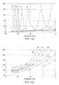
- Figure 1(a) is a graph showing the real part of an antenna's impedance, under simulations in which the relative permittivity ⁇ r of the surrounding material is varied between 1 and 10. Plotted on a relative scale against frequency, is the imaginary part 1 of the antenna impedance, tuned to a frequency of around about 960 MHz, surrounded by air or another medium having a relative permittivity ⁇ r equal to unity. Also shown on the graph are plots 2-6 of the impedances of the same antenna, when surrounded by a medium having relative permittivity value ⁇ r of 2.8, 4.6, 6.4, 8.2, and 10 respectively.
- a small change in a relative permittivity ⁇ r could cause a tag to fail to receive a wake-up signal from a transmitter or reader.
- FIG. 1(b) shown at Figure 1(b) is a graph showing the imaginary part of an antenna's impedance under the same simulated conditions. It is noted that the real part of the charge pump impedance can be adjusted by tuning the conduction angle of the rectifiers to the antenna. Such a tuning method is described in the current Applicant's co-pending but not prepublished US patent application 12/650,698 , the entire contents of which are incorporated herein by reference. The graph shows that the local maximum in the real part of the impedance occurs at reducing frequencies, again ranging from just under 1 GHz to around 500 MHz, as the relative permittivity ⁇ r increases from unity to 10.
- FIG. 2 shows a simplified schematic of a non-contact communication device according to embodiments of the invention.
- a non-contact communication device 20 comprising: an antenna 22 having a matching coil Lant and being for receiving an AC signal 24 having a voltage and a current, a main unit 26 comprising a power-extraction unit 27 and a communication unit 28 and having a main unit impedance, a tuning circuit 30 and a matching network for matching the antenna impedance to the main unit impedance.
- the tuning circuit comprises a phase detector 32 for detecting a phase difference between the voltage and the current and is configured to adjust the impedance of the matching network in dependence on the phase difference.
- the phase detector 32 comprises a passive mixer 34 which is connected across the antenna 22, and a second passive mixer 35, the inputs to which are both provided from one antenna connection.
- the passive mixers 34 and 35 provide a phase quadrature error signal to the differential amplifier 36.
- the output from differential amplifier 36 is routed to a quantiser comprising a comparator 38; the input is compared to a reference value Vref, and the output of the comparison is directed to a counter 40, to either increment or decrement the counter depending on the result of the comparison.
- the counter is used by a digital control block (not shown) to change the capacitance value of the capacitance C which is comprised in the matching network for the antenna 22.
- the power unit 27 contains a charge pump; the communication unit 28 typically comprises at least a part of the tag integrated circuit, which performs demodulation and modulation functions; in other devices the communication unit 28 may include storage capability, and may include processing capability in order to perform calculations or manipulate the modulated data transmitted by a reader (not shown), and to provide the results of the calculations or data manipulation.
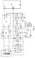
- FIG 3 shows a more detailed schematic of a non-contact communication device according to embodiments of the invention, and shows in addition to the detail of Figure 2 , the interconnections between components, comprising RF connections (shown dotted in Figure 3 ), dc power supply connections (shown solid), digital data communication lines (shown dot-dashed), and analog data communication (shown dashed).
- RF connections shown dotted in Figure 3
- dc power supply connections shown solid
- digital data communication lines shown dot-dashed
- analog data communication shown dashed.
- antenna 22 has RF connection lines to the phase detector 32, and to the capacitor bank 42 which provides a selectable capacitance C and an RF-to-DC converter 27, which as shown may be a charge pump.
- the RF connections between the antenna and phase detector provide separate information on the voltage across the antenna and the current through it (shown as rfs and rfp).
- the phase detector 32 provides a phase quadrature error signal to the comparator 38.
- the comparator provides a digital signal to the digital counter and state machine 40', which analog signal indicates either an increment or decrement.
- the digital counter and state machine (which forms a digital control block), sends a signal to the capacitor bank 42, to adjust its capacitance value, either increasing or decreasing it, by selecting an appropriate combination of capacitors, some or all of which may be switched in or out of capacitance C.
- the digital signal to the capacitor is a 6-bit word, so the capacitance can be selected to any one of 2 6 values (that is to say, to any one of 64 values); however, in other embodiments, shorter or longer word lengths may be used, to provide greater or lesser resolution for the impedance matching.
- the timing of counter 40' is controlled by means of clock 44, which provides a clock signal (clk) to the counter.
- a supply regulator (LDO) 46 provides a stable digital supply to the digital circuits, while the power-on-reset (POR) 48 triggers the tuning process when the supply voltage at the first output of the charge pump 27 is higher than 1.0V
- Shown in Figure 3 associated with some of the blocks or units, is a current value in nA.
- These values represent, for an example embodiment, the current requirement of each of the units.
- the phase detector may have a current requirement of 100nA
- comparator 38 may have a current requirement of 15nA
- the clock generator 44 may have a current requirement of 200 nA
- the LDO 46 a requirement of 50 nA
- the POR 48 a requirement for 10 nA.
- These blocks or units may be required according to embodiments of the invention, but are not necessarily present in conventional devices.
- the impedance-matching tuning by means of a phase detector according to embodiments of the invention may consume (100 + 50 + 200 + 50 + 10), that is to say, 410 nA.
- Embodiments of the invention include modifications to the power extraction unit 27, compared with those known in conventional devices, in order to ensure that, when the antenna is badly detuned from the RF field, resulting in a significant mismatch, the tuning circuitry can be provided with sufficient power in order to tune the antenna.
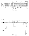
- Figure 4(a) shows an example geometrical arrangement of an antenna attached to the non-contact communication IC
- Figure 4(b) shows the equivalent circuit of the configuration of Figure 4(a)
- the antenna comprises a combination of a dipole 50 and a matching network 58.
- the dipole is shown as a meander structure, but may assume other known geometries, as will be immediately apparent to the skilled person.
- the dipole 50 shown on the left side of the antenna is connected, by means of an arm 52, to a matching network 58.
- Two loop sections (or stubs) are implemented onto the matching network.
- a first loop section is an elongate loop having first arm 54a, end angle 54b and return arm 54c. Return arm 54c is partially split, by means of slot 56, so as to enable two separate connections to the IC 54.
- IC 54 is shown mounted on the matching network.
- the IC pin rfs is connected to the antenna via 52 and to the matching network via 53, the IC pin rfp is connected to the matching network at 62 and the rfn pin is connected at 60.
- the coil L10 depicted in Figure 4(b) is part of the matching network 55, and is also used to sense the current flowing into the charge pump.
- the coils L8 and L10 (corresponding to 56 and 55 in Figure 4a , respectively) are also helping to transform the capacitance of the front-end to a much smaller value compared to the capacitance of the antenna. This allows maximizing the tuning range of the resonance frequency of the RLC network.
- FIG. 5(a) shows the circuit diagram of an example charge pump, a detail of which is shown in enlarged in Figure 5(b) .
- the charge pump may be provided as the power extraction unit 27, in embodiments of the invention.
- the charge pump comprises a linked series of stages, one of which is shown in greater detail in Figure 5(b) .
- the stage comprises a series-connected pair of diodes DS1 and DS2 connected between the stage input Si and the stage output So.
- a first stage capacitor CS1 is connected between the node between the diodes and the input voltage rail rfp, and the second stage capacitor CS2 is connected between the output and the ground (or return) rail.
- Such a multistage charge pump will be familiar to the skilled person.
- the charge pump configuration of Figure 5(a) includes a power unit (hereinafter referred to as the second power unit) consisting of a multistage charge pump, together with another power unit (hereinafter referred to as the first power unit) comprising a further multistage charge pump.
- the second power unit has five stages, whereas the first power unit has three extra stages.
- each power unit may have more or fewer stages.
- the second power unit also has a longer time constant than first power unit due to a large storage capacitance CS3 connected at its output.
- the first power unit having more stages, is able to extract power from a weaker received signal, sufficient to operate the tuning circuit according to embodiments of the invention.
- the second power unit can be made operable, to provide power to the rest of the tag, including the communication functions, and data storage and manipulation if the tag is desired for such.
- the charge pump may be configured as shown such that the second power unit does not provide any power to the tuning circuit or matching network; in other embodiments, the second power unit may be arranged so as to act as an auxiliary power source to the tuning circuit and matching network.
- FIG. 6 shows a circuit diagram of am example capacitor bank for use in embodiments of the invention.
- This type of capacitor bank will be familiar to the skilled person, and forms a selectable capacitance: it comprises a set of capacitors, some of which can be switched in and out of the circuit.
- the capacitor C0 to C5 are switchably connectable in parallel with Cmin, by means of switches MN0 -MN5, which may be MOSFETs as shown.
- Figure 7 shows a flow diagram of a method of operating a non-contact communication device according to embodiments of the invention.
- the communication unit is in a power-down mode
- the self tuning circuit is in power-down mode, except for the LDO and the POR circuit that generates a power-on reset signal (POR) when vdda exceeds 1V; in this state the current consumption may be less than 50 nA.
- the digital control block interrogates whether vdda > 1.0V: if "no" the interrogation is completed, whereas if "yes” the control moves to the next state 76.
- the controller will wait until the supply voltage of the tuning circuit exceeds 1V and then activates the tuning circuit.
- the tuning circuit is in either power-on or hold mode.
- the oscillator, phase detector, comparator, and digital block are switched on, but the remainder of the tag functionality such as the communication unit is not switched on.
- the current consumption in this mode is typically thus less than 400 nA. This allows compensation for a large amount of power mismatch.
- control then waits for a predetermined number, L, of clock cycles in order to allow the analog circuits time to settle before starting the tuning process.
- L clock cycles which is determined by interrogation 78
- control moves to state 80, wherein the tuning is in active mode. Tuning of the matching network as described above is then carried out.
- the control interrogates at interrogation 82, whether the second power unit, for powering the communication functionality of the tag has reached a voltage greater than 1V (i.e. whether vdda_tag > 1V). Once this condition is achieved, control moves to state 84, wherein the self-tuning is put into hold mode and the communication unit and other associated tag functionality is in power on mode. This allows reducing the response time of the tag to the reader request.
- the tag communication circuit is now powered on, but stays in the hold mode until the tuning is completed in order not to interfere with the tuning process. However, the current consumption at this stage will still typically be less than 3 pA. In the examples shown, a further M clock cycles are allowed to pass in order to allow the system to settle. This is checked by means of interrogation 86, and once this period has elapsed, control moves to state 88, in which the tuning reverts from pause mode to active mode in order to continue the self tuning. Tuning is allowed to continue until a total of N clock cycles have passed (which is checked at interrogation box 90), at which point the tuning is deemed to be completed, at box 92. At this moment the tuning circuits are forced in the power-down mode, except for the LDO which stays in the power-on mode, and the communication link between the tag and the power-providing reader can be established.
- Figure 8 shows simulation results of a situation where the antenna inductance is initially too large, and is retuned by means of a tuning circuit in accordance with embodiments of the invention.
- the Figure shows several voltages (plotted in V), and the switched-in fraction of the capacitor bank, plotted against time (in ⁇ S), as follows: curve 801 is the supply voltage of the tuning circuit (vdda), and curve 802 is the main supply voltage of the tag (vdda_tag), to power for instance the communication functionality.
- Curve 803 is the tuning word of the capacitor bank; and curve 804 is the output of the phase detector. Transitions in the comparator output from high to low (or vice versa) are shown at 805, and the moments at which the tuning circuit, and the main power unit, are enabled are shown at moments 806 and 807 respectively.
- the capacitor bank is set to 50% capacitance.
- the supply to the tuning circuit is sufficient to switch the tuning circuit on.
- the phase detector determines that the quadrature error is too high, and the counter starts to instruct the capacitor bank to reduce the tuning word 803 for the capacitance in small steps.
- the charge pump has achieved sufficient power to the switch on the main circuitry of the tag, and there is another brief settling period during which the decrementing of the capacitor word is interrupted.
- the increase in the capacitor bank has the effect of a reduction in the phase difference 804; once quadrature is reached, the comparator goes high, resulting in an increment in the tuning word 803 controlling the capacitance. This continual adjustment up-and-down of the phase continues until the tuning is stopped at the end of a tuning phase.
- the tag communication circuit switches thereafter form a hold mode, for the listen or receive mode.
- Figure 9 shows simulation results in a situation where the antenna inductance is initially too small, and is retuned by means of a tuning circuit in accordance with embodiments of the invention.
- the curves generally corresponds to those shown in Figure 8 , such that curve 901 is the supply voltage of the tuning circuit (vdda), curve 902 the main supply voltage of the tag (vdda_tag), curve 903 the tuning word of the capacitor bank, and curve 904 the output of the phase detector.
- the moments at which the tuning circuit, and the main power unit, are enabled are shown at moments 906 and 907 respectively.
Landscapes
- Engineering & Computer Science (AREA)
- Computer Hardware Design (AREA)
- Microelectronics & Electronic Packaging (AREA)
- Physics & Mathematics (AREA)
- General Physics & Mathematics (AREA)
- Theoretical Computer Science (AREA)
- Computer Networks & Wireless Communication (AREA)
- Near-Field Transmission Systems (AREA)
Abstract
Also disclosed is a method for tuning a non-contact communication device.
Description
- This invention relates to non-contact communication devices, and to methods of operating non-contact communication devices.
- Non-contact communication devices are widely used in a range of applications, such as stock control and inventory management, item tracking, security, and the like. Since a basic function of non-contact communication devices is identification of the device or tag, and radio frequencies are used, this technology is also known as RFID (radio frequency identification devices), although should be noted that applications now considerably extend beyond mere simple identification function. Hereinbelow, non-contact communication and RFID shall be used synonymously.
- RFID generally has two main components: a device, which may be, for instance, in the form of a tag, or embedded in a card, chip, or other item, and a reader. Hereinbelow, the term tag will be used to indicate any configuration of the device. In a typical arrangement, the reader transmits a RF AC signal at a frequency which may typically be in the range of 125-148.5 kHz (low frequency - LF), around 13.56 MHz (high frequency - HF), or between 300 MHz and 3 GHz (ultrahigh frequency - UHF). The exact frequency ranges used depend on the regulatory requirements of the country or region for which the reader and tags are designed. The tag typically modulates the RF signal, and retransmits or backscatters it back to the reader. The reader detects the return modulated signal, and demodulates it in order to extract information from the tag. In more advanced non-contact communication devices, the reader may provide information to the tag within the RF signal, and the tag may process or store this information and may provide a response thereto.
- Tags may be either passive, or active. An active tag has its own power supply, to power for instance the modulation circuitry. However, providing an on-board power supply is relatively expensive and they are relatively bulky: therefore, passive tags are more widely used. Passive tags do not have their own power supply, but rather extract power from an external source, which is most typically the RF field. Although this invention relates primarily to passive tags, it may also find application in active tags, for instance to avoid or reduce Bit Error Rate (BER) losses under detuned conditions.
- Passive tags, and in particular passive UHF tags, generally have a higher "read range" - that is to say, the distance between tag and reader over which the tag can communicate - than other tags. However, for all tags, and passive tags in particular, the read range can be affected by environmental factors, which may detune the tag, thus modifying its operating frequency and potentially reducing the received power.
- An RFID tag's performance, assuming constant power consumption in its integrated circuit (IC), depends on the amount of power that can be captured by the antenna and provided to the IC. This in turn depends on impedance matching between the antenna and the IC. Environmental factors such as the presence of metals, liquids or other materials, or the close proximity of further tags, may lead to absorption or parasitic capacitance, which can the result in detuning the tag. Detuning of the tag may also result from the process spread in manufacturing of, for instance, any of the chip, antenna or packaging.
- It has been proposed in United States Patent
US7,167,090 to provide a feedback tuning circuit, to mitigate the problem of detuning. The tuning circuit alters the impedance of the impedance matching network coupling the antenna to rest of the device, in order to maximise the RF input signal and thereby optimise the performance of a power extraction circuit. - However, such a circuit is sensitive to noise on the amplitude modulation (AM) signal, variation in transmitter power, and changes in the surrounding environment of the tag.
- It is an object of the present invention to provide an alternative non-contact communication device which can be tuned.
- According to a first aspect of the present invention, there is provided a non-contact communication device comprising : an antenna having an antenna impedance and being for receiving an AC signal having a voltage and a current, a main unit comprising a power-extraction unit and a communication unit and having a main unit impedance, a tuning circuit, and a matching network for matching the antenna impedance to the main unit impedance, characterised in that the tuning circuit comprises a phase detector for detecting a phase difference between the voltage and the current and is configured to adjust the impedance of the matching network in dependence on the phase difference.
- Use of a phase detector results in a device which is less sensitive to amplitude modulated noise than known devices, since noise tends to have a more significant impact on the amplitude than the phase of the input RF signal.
- In embodiments, the matching network comprises a capacitor bank for providing a selectable capacitance and the tuning circuit is configured to adjust the impedance of the matching network so as to minimise the quadrature phase error, by selecting the capacitance of the matching network. By quadrature phase error, is meant the amount by which the phases are not in quadrature. For instance, if the first phase leads the second phase by a phase difference of π/3, then the out-of-quadrature phase difference is π/6, being the difference between π/3 and a quadrature phase of π/2. The quadrature phase error may also be termed out-of-quadrature phase difference.
- In embodiments the phase detector is a passive phase detector. A passive phase detector does not require the relatively high level of energy typically required by active phase detectors. For active tags this energy may be available, but is unlikely to be available to passive tags, in which the use of a passive phase detector thus may provide a significant advantage.
- In embodiments, the phase detector detects a phase difference between the input voltage and the input current by detecting the phase difference between the input voltage and a coil voltage across a matching coil (L8), which matching coil forms part of the antenna (22)
- In embodiments, the power-extraction unit comprises a first output for providing power to the tuning circuit and a second output for providing power to the communication unit. Thereby, the tuning can operate to match the impedance, under badly detuned conditions, or other conditions where there is not sufficient power available to operate the complete tag.
- In embodiments, the power extraction unit is an RF-to-DC converter and may in particular be a charge pump.
- In embodiments, the first power output has at least one of more stages and a smaller time constant than the second power output. Using more stages for the first output helps to build quickly sufficient voltage under detuning conditions. A smaller time constant helps to speedup the tuning process. Faster response is thereby facilitated, which is beneficial, since a tag should be able to respond to the reader command within a given amount of time.
- In embodiments, the tuning circuit further comprises a quantiser for quantising the output of the phase detectors and for providing an input to a counter, which counter is configured to select the capacitance of the matching network.
- According to another aspect of the present invention, there is provided a method of operating a non-contact communication device, the method comprising: receiving an AC signal at an antenna; extracting power from the AC signal; using at least a part of the extracted power to tune the device by: detecting a phase difference between a voltage and a current of the AC signal in a phase detector, and adjusting a matching network in dependence on the phase.
- In embodiments, adjusting the matching network in dependence on the phase comprises quantising an output of the phase detector, adjusting a counter in response to the quantisation, and selecting the capacitance of a capacitor bank in dependence on the counter.
- In embodiments, the method may further comprise, subsequent to tuning the device, using a further part of the extracted power to power a communication unit.
- These and other aspects of the invention will be apparent from, and elucidated with reference to, the embodiments described hereinafter.
- Embodiments of the invention will be described, by way of example only, with reference to the drawings, in which
-
Figure 1(a) is a graph showing the real part of an antenna's impedance, under simulations in which the permittivity εr of the surrounding material is varied between 1 and 10; -
Figure 1(b) is a graph showing the imaginary part of an antenna's impedance under the same simulated conditions; -
Figure 2 shows a simplified schematic of a non-contact communication device according to embodiments of the invention; -
Figure 3 shows a more detailed schematic of a non-contact communication device according to embodiments of the invention; -
Figure 4(a) shows an example geometrical arrangement of an antenna attached to a non-contact communication IC; -
Figure 4(b) shows the equivalent circuit of the configuration offigure 4(a) ; -
Figure 5 shows the circuit diagram of an example charge pump; -
Figure 6 shows a circuit diagram of a capacitor bank for use in embodiments of the invention; -
Figure 7 shows a flow diagram of a method of operating a noncontact communication device according to embodiments of the invention; -
Figure 8 shows simulation results of a situation where the antenna inductance is initially too large, and is retuned by means of a tuning circuit in accordance with embodiments of the invention; -
Figure 9 shows simulation results in a situation where the antenna inductance is initially too small, and is retuned by means of a tuning circuit in accordance with embodiments of the invention. - It should be noted that the Figures are diagrammatic and not drawn to scale. Relative dimensions and proportions of parts of these Figures have been shown exaggerated or reduced in size, for the sake of clarity and convenience in the drawings. The same reference signs are generally used to refer to corresponding or similar feature in modified and different embodiments
-
Figure 1(a) is a graph showing the real part of an antenna's impedance, under simulations in which the relative permittivity εr of the surrounding material is varied between 1 and 10. Plotted on a relative scale against frequency, is theimaginary part 1 of the antenna impedance, tuned to a frequency of around about 960 MHz, surrounded by air or another medium having a relative permittivity εr equal to unity. Also shown on the graph are plots 2-6 of the impedances of the same antenna, when surrounded by a medium having relative permittivity value εr of 2.8, 4.6, 6.4, 8.2, and 10 respectively. From the graph it is clear that although the magnitude of the peak in the impedance does not vary significantly, the frequency at which the peak occurs, that is to say the tuned frequency of the antenna, reduces from the value around 960 MHz, in thecase 1 where the relative permittivity εr is unity, to about 500 MHz forplot 6 in which the relative permittivity εr is 10. Thus a change in relative permittivity has a significant impact on the tuned frequency of the antenna. - Thus, a small change in a relative permittivity εr could cause a tag to fail to receive a wake-up signal from a transmitter or reader.
- For completeness, shown at
Figure 1(b) is a graph showing the imaginary part of an antenna's impedance under the same simulated conditions. It is noted that the real part of the charge pump impedance can be adjusted by tuning the conduction angle of the rectifiers to the antenna. Such a tuning method is described in the current Applicant's co-pending but not prepublishedUS patent application 12/650,698 -
Figure 2 shows a simplified schematic of a non-contact communication device according to embodiments of the invention. Shown in the Figure is anon-contact communication device 20 comprising: anantenna 22 having a matching coil Lant and being for receiving anAC signal 24 having a voltage and a current, amain unit 26 comprising a power-extraction unit 27 and acommunication unit 28 and having a main unit impedance, atuning circuit 30 and a matching network for matching the antenna impedance to the main unit impedance. The tuning circuit comprises aphase detector 32 for detecting a phase difference between the voltage and the current and is configured to adjust the impedance of the matching network in dependence on the phase difference. - As shown in
Figure 2 , thephase detector 32 comprises apassive mixer 34 which is connected across theantenna 22, and a secondpassive mixer 35, the inputs to which are both provided from one antenna connection. Thepassive mixers differential amplifier 36. The output fromdifferential amplifier 36 is routed to a quantiser comprising acomparator 38; the input is compared to a reference value Vref, and the output of the comparison is directed to acounter 40, to either increment or decrement the counter depending on the result of the comparison. The counter is used by a digital control block (not shown) to change the capacitance value of the capacitance C which is comprised in the matching network for theantenna 22. Thepower unit 27 contains a charge pump; thecommunication unit 28 typically comprises at least a part of the tag integrated circuit, which performs demodulation and modulation functions; in other devices thecommunication unit 28 may include storage capability, and may include processing capability in order to perform calculations or manipulate the modulated data transmitted by a reader (not shown), and to provide the results of the calculations or data manipulation. -
Figure 3 shows a more detailed schematic of a non-contact communication device according to embodiments of the invention, and shows in addition to the detail ofFigure 2 , the interconnections between components, comprising RF connections (shown dotted inFigure 3 ), dc power supply connections (shown solid), digital data communication lines (shown dot-dashed), and analog data communication (shown dashed). Like blocks are assigned like reference numerals toFigure 2 : thus,antenna 22 has RF connection lines to thephase detector 32, and to the capacitor bank 42 which provides a selectable capacitance C and an RF-to-DC converter 27, which as shown may be a charge pump. Due to the design of the antenna, which will be described in more detail herebelow with reference toFigure 4 , the RF connections between the antenna and phase detector provide separate information on the voltage across the antenna and the current through it (shown as rfs and rfp). Thephase detector 32 provides a phase quadrature error signal to thecomparator 38. The comparator provides a digital signal to the digital counter and state machine 40', which analog signal indicates either an increment or decrement. The digital counter and state machine (which forms a digital control block), sends a signal to the capacitor bank 42, to adjust its capacitance value, either increasing or decreasing it, by selecting an appropriate combination of capacitors, some or all of which may be switched in or out of capacitance C. As shown, the digital signal to the capacitor is a 6-bit word, so the capacitance can be selected to any one of 26 values (that is to say, to any one of 64 values); however, in other embodiments, shorter or longer word lengths may be used, to provide greater or lesser resolution for the impedance matching. - The timing of counter 40' is controlled by means of clock 44, which provides a clock signal (clk) to the counter. A supply regulator (LDO) 46 provides a stable digital supply to the digital circuits, while the power-on-reset (POR) 48 triggers the tuning process when the supply voltage at the first output of the
charge pump 27 is higher than 1.0V - Shown in
Figure 3 , associated with some of the blocks or units, is a current value in nA. These values represent, for an example embodiment, the current requirement of each of the units. In particular, the phase detector may have a current requirement of 100nA,comparator 38 may have a current requirement of 15nA, the clock generator 44 may have a current requirement of 200 nA, the LDO 46 a requirement of 50 nA, and the POR 48 a requirement for 10 nA. These blocks or units may be required according to embodiments of the invention, but are not necessarily present in conventional devices. Thus the impedance-matching tuning by means of a phase detector according to embodiments of the invention may consume (100 + 50 + 200 + 50 + 10), that is to say, 410 nA. Embodiments of the invention include modifications to thepower extraction unit 27, compared with those known in conventional devices, in order to ensure that, when the antenna is badly detuned from the RF field, resulting in a significant mismatch, the tuning circuitry can be provided with sufficient power in order to tune the antenna. -
Figure 4(a) shows an example geometrical arrangement of an antenna attached to the non-contact communication IC, andFigure 4(b) shows the equivalent circuit of the configuration ofFigure 4(a) . The antenna comprises a combination of adipole 50 and a matching network 58. The dipole is shown as a meander structure, but may assume other known geometries, as will be immediately apparent to the skilled person. Thedipole 50 shown on the left side of the antenna is connected, by means of anarm 52, to a matching network 58. Two loop sections (or stubs) are implemented onto the matching network. A first loop section is an elongate loop havingfirst arm 54a, end angle 54b and return arm 54c. Return arm 54c is partially split, by means ofslot 56, so as to enable two separate connections to theIC 54. - In the
Figure 4(a) ,IC 54 is shown mounted on the matching network. The IC pin rfs is connected to the antenna via 52 and to the matching network via 53, the IC pin rfp is connected to the matching network at 62 and the rfn pin is connected at 60. The coil L10 depicted inFigure 4(b) is part of thematching network 55, and is also used to sense the current flowing into the charge pump. The coils L8 and L10 (corresponding to 56 and 55 inFigure 4a , respectively) are also helping to transform the capacitance of the front-end to a much smaller value compared to the capacitance of the antenna. This allows maximizing the tuning range of the resonance frequency of the RLC network. -
Figure 5(a) shows the circuit diagram of an example charge pump, a detail of which is shown in enlarged inFigure 5(b) . The charge pump may be provided as thepower extraction unit 27, in embodiments of the invention. The charge pump comprises a linked series of stages, one of which is shown in greater detail inFigure 5(b) . The stage comprises a series-connected pair of diodes DS1 and DS2 connected between the stage input Si and the stage output So. A first stage capacitor CS1 is connected between the node between the diodes and the input voltage rail rfp, and the second stage capacitor CS2 is connected between the output and the ground (or return) rail. Such a multistage charge pump will be familiar to the skilled person. However, the charge pump configuration ofFigure 5(a) , as used in embodiments of the invention, includes a power unit (hereinafter referred to as the second power unit) consisting of a multistage charge pump, together with another power unit (hereinafter referred to as the first power unit) comprising a further multistage charge pump. In this specific embodiment shown, the second power unit has five stages, whereas the first power unit has three extra stages. Of course, in other embodiments, each power unit may have more or fewer stages. In the embodiment shown, the second power unit also has a longer time constant than first power unit due to a large storage capacitance CS3 connected at its output. The first power unit, having more stages, is able to extract power from a weaker received signal, sufficient to operate the tuning circuit according to embodiments of the invention. Once the matching circuit has been tuned, the second power unit can be made operable, to provide power to the rest of the tag, including the communication functions, and data storage and manipulation if the tag is desired for such. The charge pump may be configured as shown such that the second power unit does not provide any power to the tuning circuit or matching network; in other embodiments, the second power unit may be arranged so as to act as an auxiliary power source to the tuning circuit and matching network. -
Figure 6 shows a circuit diagram of am example capacitor bank for use in embodiments of the invention. This type of capacitor bank will be familiar to the skilled person, and forms a selectable capacitance: it comprises a set of capacitors, some of which can be switched in and out of the circuit. In the embodiment shown, there are six capacitors, C0 through C5, with a total capacitance Cmax, which corresponds to the maximum capacitance which the capacitor bank can have. Capacitors C0 toC5, have capacitance which increase in a binary fashion, such that


The capacitor C0 to C5 are switchably connectable in parallel with Cmin, by means of switches MN0 -MN5, which may be MOSFETs as shown. -
Figure 7 shows a flow diagram of a method of operating a non-contact communication device according to embodiments of the invention; - In an
initial state 72, the communication unit is in a power-down mode, the self tuning circuit is in power-down mode, except for the LDO and the POR circuit that generates a power-on reset signal (POR) when vdda exceeds 1V; in this state the current consumption may be less than 50 nA. At decision 74, the digital control block interrogates whether vdda > 1.0V: if "no" the interrogation is completed, whereas if "yes" the control moves to thenext state 76. Thus at block 74, the controller will wait until the supply voltage of the tuning circuit exceeds 1V and then activates the tuning circuit. At 76, the tuning circuit is in either power-on or hold mode. Thus the oscillator, phase detector, comparator, and digital block are switched on, but the remainder of the tag functionality such as the communication unit is not switched on. The current consumption in this mode is typically thus less than 400 nA. This allows compensation for a large amount of power mismatch. - The system then waits for a predetermined number, L, of clock cycles in order to allow the analog circuits time to settle before starting the tuning process. Once L clock cycles have passed, which is determined by
interrogation 78, control moves tostate 80, wherein the tuning is in active mode. Tuning of the matching network as described above is then carried out. Meantime, the control interrogates atinterrogation 82, whether the second power unit, for powering the communication functionality of the tag has reached a voltage greater than 1V (i.e. whether vdda_tag > 1V). Once this condition is achieved, control moves tostate 84, wherein the self-tuning is put into hold mode and the communication unit and other associated tag functionality is in power on mode. This allows reducing the response time of the tag to the reader request. The tag communication circuit is now powered on, but stays in the hold mode until the tuning is completed in order not to interfere with the tuning process. However, the current consumption at this stage will still typically be less than 3 pA. In the examples shown, a further M clock cycles are allowed to pass in order to allow the system to settle. This is checked by means ofinterrogation 86, and once this period has elapsed, control moves tostate 88, in which the tuning reverts from pause mode to active mode in order to continue the self tuning. Tuning is allowed to continue until a total of N clock cycles have passed (which is checked at interrogation box 90), at which point the tuning is deemed to be completed, atbox 92. At this moment the tuning circuits are forced in the power-down mode, except for the LDO which stays in the power-on mode, and the communication link between the tag and the power-providing reader can be established. -
Figure 8 shows simulation results of a situation where the antenna inductance is initially too large, and is retuned by means of a tuning circuit in accordance with embodiments of the invention. The Figure shows several voltages (plotted in V), and the switched-in fraction of the capacitor bank, plotted against time (in µS), as follows:curve 801 is the supply voltage of the tuning circuit (vdda), andcurve 802 is the main supply voltage of the tag (vdda_tag), to power for instance the communication functionality.Curve 803 is the tuning word of the capacitor bank; andcurve 804 is the output of the phase detector. Transitions in the comparator output from high to low (or vice versa) are shown at 805, and the moments at which the tuning circuit, and the main power unit, are enabled are shown atmoments - Initially, at power-on the capacitor bank is set to 50% capacitance. At
moment 806 the supply to the tuning circuit is sufficient to switch the tuning circuit on. After a relatively short settling time, the phase detector determines that the quadrature error is too high, and the counter starts to instruct the capacitor bank to reduce thetuning word 803 for the capacitance in small steps. Atmoment 807 the charge pump has achieved sufficient power to the switch on the main circuitry of the tag, and there is another brief settling period during which the decrementing of the capacitor word is interrupted. The increase in the capacitor bank has the effect of a reduction in thephase difference 804; once quadrature is reached, the comparator goes high, resulting in an increment in thetuning word 803 controlling the capacitance. This continual adjustment up-and-down of the phase continues until the tuning is stopped at the end of a tuning phase. The tag communication circuit switches thereafter form a hold mode, for the listen or receive mode. -
Figure 9 shows simulation results in a situation where the antenna inductance is initially too small, and is retuned by means of a tuning circuit in accordance with embodiments of the invention. The curves generally corresponds to those shown inFigure 8 , such thatcurve 901 is the supply voltage of the tuning circuit (vdda),curve 902 the main supply voltage of the tag (vdda_tag),curve 903 the tuning word of the capacitor bank, andcurve 904 the output of the phase detector. The moments at which the tuning circuit, and the main power unit, are enabled are shown atmoments - A generally similar sequence is shown in
Figure 9 to that inFigure 9 , with the difference that in this case, initially thequadrature phase error 904 is negative, which results in theword 903 controlling the capacitance in the capacitor bank gradually increasing until quadrature is achieved. Settling periods for the system, during which there is a pause in the incrementing of theword 903, are visible after the first and second power units are switched on. - From reading the present disclosure, other variations and modifications will be apparent to the skilled person. Such variations and modifications may involve equivalent and other features which are already known in the art of non-contact communication and RFID, and which may be used instead of, or in addition to, features already described herein.
- Although the appended claims are directed to particular combinations of features, it should be understood that the scope of the disclosure of the present invention also includes any novel feature or any novel combination of features disclosed herein either explicitly or implicitly or any generalisation thereof, whether or not it relates to the same invention as presently claimed in any claim and whether or not it mitigates any or all of the same technical problems as does the present invention.
- Features which are described in the context of separate embodiments may also be provided in combination in a single embodiment. Conversely, various features which are, for brevity, described in the context of a single embodiment, may also be provided separately or in any suitable sub-combination.
- The applicant hereby gives notice that new claims may be formulated to such features and/or combinations of such features during the prosecution of the present application or of any further application derived therefrom.
- For the sake of completeness it is also stated that the term "comprising" does not exclude other elements or steps, the term "a" or "an" does not exclude a plurality, a single processor or other unit may fulfil the functions of several means recited in the claims and reference signs in the claims shall not be construed as limiting the scope of the claims.
Claims (11)
- A non-contact communication device (20) comprising :an antenna (22) having an antenna impedance and being for receiving an AC signal having an input voltage and an input current,a main unit (26) comprising a power-extraction unit (27) and a communication unit (28) and having a main unit impedance,a tuning circuit (30), anda matching network for matching the antenna impedance to the main unit impedance,characterised in thatthe tuning circuit (30) comprises a phase detector for detecting a phase difference between the input voltage and the input current and is configured to adjust the impedance of the matching network in dependence on the phase difference.
- A non-contact communication device as claimed in claim 1, wherein the matching network comprises a capacitor bank (42) for providing a selectable capacitance and the tuning circuit (30) is configured to adjust the impedance of the matching network so as to minimise the quadrature phase error, by selecting the capacitance of the matching network.
- A non-contact communication device as claimed in claim 1 or 2 wherein the phase detector is a passive phase detector.
- A non-contact communication device as claimed in any preceding claim, wherein the phase detector detects a phase difference between the input voltage and the input current by detecting the phase difference between the input voltage and a coil voltage across a matching coil (L8), which matching coil forms part of the antenna (22)
- A non-contact communication device as claimed in any preceding claim, wherein the power-extraction unit (27) comprises a first output (vdda) for providing power to the tuning circuit and a second output (vdda_tag) for providing power to the communication unit.
- A non-contact communication device as claimed in claim 5, wherein the power extraction unit (27) is a charge pump.
- A non-contact communication device as claimed in claim 6 wherein the first power output (vdda) has at least one of more stages and a smaller time constant than the second power output (vdda_tag).
- A non-contact communication device as claimed in any preceding claim, wherein the tuning circuit (30) further comprises a quantiser for quantising the output of the phase detector and for providing an input to a counter (40), which counter is configured to select the capacitance of the matching network.
- A method of operating a non-contact communication device, the method comprising:receiving an AC signal at an antenna;extracting power from the AC signal;using at least a part of the extracted power to tune the device by:detecting a phase difference between a voltage and a current of the AC signal in a phase detector, andadjusting a matching network in dependence on the phase.
- The method of claim 9 wherein adjusting the matching network in dependence on the phase comprises
quantising an output of the phase detector,
adjusting a counter in response to the quantisation, and
selecting the capacitance of a capacitor bank in dependence on the counter. - The method of claim 9 or 10, further comprising, subsequent to tuning the device, using a further part of the extracted power to power a communication unit.
Priority Applications (3)
| Application Number | Priority Date | Filing Date | Title |
|---|---|---|---|
| EP10159383A EP2375363B1 (en) | 2010-04-08 | 2010-04-08 | Non-contact communication device and method of operating the same |
| CN201110094772.2A CN102214313B (en) | 2010-04-08 | 2011-04-07 | Non-contact communication device and method of operating the same |
| US13/082,999 US8730016B2 (en) | 2010-04-08 | 2011-04-08 | Non-contact communication device and method of operating the same |
Applications Claiming Priority (1)
| Application Number | Priority Date | Filing Date | Title |
|---|---|---|---|
| EP10159383A EP2375363B1 (en) | 2010-04-08 | 2010-04-08 | Non-contact communication device and method of operating the same |
Publications (2)
| Publication Number | Publication Date |
|---|---|
| EP2375363A1 true EP2375363A1 (en) | 2011-10-12 |
| EP2375363B1 EP2375363B1 (en) | 2013-03-27 |
Family
ID=42312631
Family Applications (1)
| Application Number | Title | Priority Date | Filing Date |
|---|---|---|---|
| EP10159383A Not-in-force EP2375363B1 (en) | 2010-04-08 | 2010-04-08 | Non-contact communication device and method of operating the same |
Country Status (3)
| Country | Link |
|---|---|
| US (1) | US8730016B2 (en) |
| EP (1) | EP2375363B1 (en) |
| CN (1) | CN102214313B (en) |
Cited By (4)
| Publication number | Priority date | Publication date | Assignee | Title |
|---|---|---|---|---|
| CN103840853A (en) * | 2014-03-28 | 2014-06-04 | 上海坤锐电子科技有限公司 | Automatic impedance matching circuit suitable for radio frequency SIM card |
| CN104008415A (en) * | 2014-04-30 | 2014-08-27 | 北京邮电大学 | Self-interference canceling circuit |
| CN104008409A (en) * | 2014-04-30 | 2014-08-27 | 北京邮电大学 | Optical link for connecting antenna with reader-writer in passive RFID system |
| WO2025032357A1 (en) * | 2023-08-07 | 2025-02-13 | Silicon Craft Technology Public Company Limited (Sict) | A power extraction circuit for radio frequency identification (rfid) tags and power extraction method thereof |
Families Citing this family (16)
| Publication number | Priority date | Publication date | Assignee | Title |
|---|---|---|---|---|
| US11817637B2 (en) * | 2006-11-18 | 2023-11-14 | Rfmicron, Inc. | Radio frequency identification (RFID) moisture tag(s) and sensors with extended sensing via capillaries |
| US8886145B2 (en) * | 2012-03-26 | 2014-11-11 | Sony Corporation | Antenna adjustment circuit, antenna adjustment method, and communication unit |
| US9430729B2 (en) * | 2012-05-31 | 2016-08-30 | Nxp B.V. | Broadband progressive tag |
| KR20140008020A (en) * | 2012-07-10 | 2014-01-21 | 삼성전자주식회사 | Wireless power transmitter, wireless power relay device and wireless power receiver |
| EP3039770B1 (en) | 2013-08-14 | 2020-01-22 | WiTricity Corporation | Impedance tuning |
| US9584191B2 (en) | 2013-12-20 | 2017-02-28 | Southern Avionics Co. | Antenna tuning unit |
| US10002266B1 (en) | 2014-08-08 | 2018-06-19 | Impinj, Inc. | RFID tag clock frequency reduction during tuning |
| US10746682B2 (en) * | 2014-10-08 | 2020-08-18 | Rfmicron, Inc. | Wireless sensor with multiple sensing options |
| CN104966113B (en) * | 2015-07-27 | 2018-12-25 | 威海北洋电气集团股份有限公司 | The decoding of RFID read-write system and its label return signal and conflict processing method |
| CN105243347B (en) * | 2015-10-20 | 2018-05-01 | 上海汇阅物联网科技有限公司 | A kind of observation circuit based on passive label |
| CN105897312B (en) * | 2016-04-01 | 2019-04-02 | 王清斌 | An NFC tag interface optimized for energy harvesting and small size |
| IT201800002924A1 (en) * | 2018-02-21 | 2019-08-21 | St Microelectronics Srl | PROCEDURE FOR COLLECTING RADIOFREQUENCY ENERGY, CORRESPONDING CIRCUIT AND DEVICE |
| FR3114724B1 (en) * | 2020-09-30 | 2023-11-10 | St Microelectronics Rousset | Near field communication device and method |
| CN112580376B (en) * | 2020-12-14 | 2023-05-12 | 广东工业大学 | RFID tag antenna impedance tuning method and system based on software and hardware cooperation |
| US11481595B2 (en) * | 2020-12-18 | 2022-10-25 | Nxp B.V. | Dual system RFID tag |
| CN113283565B (en) * | 2021-06-02 | 2024-01-26 | 上海宜链物联网有限公司 | Automatic tuning system and method for antenna impedance of RFID tag chip |
Citations (3)
| Publication number | Priority date | Publication date | Assignee | Title |
|---|---|---|---|---|
| US5263183A (en) * | 1991-04-30 | 1993-11-16 | Seiko Corp. | Radio antenna tuning circuit |
| US6055420A (en) * | 1990-06-19 | 2000-04-25 | Bose Corproation | Antenna system having a high Q circuit |
| WO2003038733A1 (en) | 2001-10-24 | 2003-05-08 | Zentrum Mikroelektronik Dresden Ag | Method for the self-trimming of a resonance circuit |
Family Cites Families (5)
| Publication number | Priority date | Publication date | Assignee | Title |
|---|---|---|---|---|
| US7107026B2 (en) * | 2004-02-12 | 2006-09-12 | Nautel Limited | Automatic matching and tuning unit |
| US7167090B1 (en) | 2004-09-17 | 2007-01-23 | Massachusetts Institute Of Technology | Far-field RF power extraction circuits and systems |
| US7595732B2 (en) * | 2006-03-31 | 2009-09-29 | Broadcom Corporation | Power generating circuit |
| US7579902B2 (en) * | 2006-12-11 | 2009-08-25 | Atmel Corporation | Charge pump for generation of multiple output-voltage levels |
| US8643356B2 (en) * | 2009-10-06 | 2014-02-04 | Infineon Technologies Ag | Voltage regulation and modulation circuit |
-
2010
- 2010-04-08 EP EP10159383A patent/EP2375363B1/en not_active Not-in-force
-
2011
- 2011-04-07 CN CN201110094772.2A patent/CN102214313B/en not_active Expired - Fee Related
- 2011-04-08 US US13/082,999 patent/US8730016B2/en active Active
Patent Citations (3)
| Publication number | Priority date | Publication date | Assignee | Title |
|---|---|---|---|---|
| US6055420A (en) * | 1990-06-19 | 2000-04-25 | Bose Corproation | Antenna system having a high Q circuit |
| US5263183A (en) * | 1991-04-30 | 1993-11-16 | Seiko Corp. | Radio antenna tuning circuit |
| WO2003038733A1 (en) | 2001-10-24 | 2003-05-08 | Zentrum Mikroelektronik Dresden Ag | Method for the self-trimming of a resonance circuit |
Cited By (5)
| Publication number | Priority date | Publication date | Assignee | Title |
|---|---|---|---|---|
| CN103840853A (en) * | 2014-03-28 | 2014-06-04 | 上海坤锐电子科技有限公司 | Automatic impedance matching circuit suitable for radio frequency SIM card |
| CN104008415A (en) * | 2014-04-30 | 2014-08-27 | 北京邮电大学 | Self-interference canceling circuit |
| CN104008409A (en) * | 2014-04-30 | 2014-08-27 | 北京邮电大学 | Optical link for connecting antenna with reader-writer in passive RFID system |
| CN104008409B (en) * | 2014-04-30 | 2019-04-02 | 北京邮电大学 | The optical link of antenna and reader is connected in passive RFID system |
| WO2025032357A1 (en) * | 2023-08-07 | 2025-02-13 | Silicon Craft Technology Public Company Limited (Sict) | A power extraction circuit for radio frequency identification (rfid) tags and power extraction method thereof |
Also Published As
| Publication number | Publication date |
|---|---|
| CN102214313B (en) | 2014-01-29 |
| US8730016B2 (en) | 2014-05-20 |
| CN102214313A (en) | 2011-10-12 |
| EP2375363B1 (en) | 2013-03-27 |
| US20110248832A1 (en) | 2011-10-13 |
Similar Documents
| Publication | Publication Date | Title |
|---|---|---|
| EP2375363B1 (en) | Non-contact communication device and method of operating the same | |
| Shameli et al. | Power harvester design for passive UHF RFID tag using a voltage boosting technique | |
| Reinisch et al. | A multifrequency passive sensing tag with on-chip temperature sensor and off-chip sensor interface using EPC HF and UHF RFID technology | |
| US7535362B2 (en) | Circuit arrangement and method for supplying power to a transponder | |
| EP2351217B1 (en) | Tuned resonant circuits | |
| US8836512B2 (en) | Self tuning RFID | |
| US9471816B1 (en) | Increasing dynamic range of RFID tag self-tuning | |
| EP3968210B1 (en) | Rfid tag information reading device and method | |
| US9646186B1 (en) | Rectifier biasing for self-tuning RFID tags | |
| EP1738301A1 (en) | Variable frequency radio frequency identification (rfid) tags | |
| US8840023B2 (en) | Self-parameterising RFID antenna extender | |
| EP2669851B1 (en) | Broadband progressive tag | |
| US20180358680A1 (en) | Method of Monitoring the Level of Power Transmitted by a Contactless Communication Device and Corresponding Contactless Communication Device | |
| Lee et al. | Design consideration of UHF RFID tag for increased reading range | |
| CN102868237A (en) | Circuit for improving energy transmission efficiency of non-contact type IC (integrated circuit) card | |
| Li et al. | A 13.56 MHz RFID transponder front-end with merged load modulation and voltage doubler-clamping rectifier circuits | |
| WO1996028880A2 (en) | Transponder for electronic identification system | |
| Seigneuret et al. | Auto-tuning in passive UHF RFID tags | |
| CN113792563B (en) | Dual-mode radio frequency identification sensor, system and working method | |
| Zuriarrain et al. | A CMOS low frequency analog RFID front-end for the IoT | |
| Neto et al. | A semi-passive UHF RFID tag compliant with Brazilian national automated vehicle identification system (SINIAV) | |
| Bakhtiar et al. | An RF power harvesting system with input-tuning for long-range RFID tags | |
| EP3196807B1 (en) | Smart objects | |
| WO2024178568A1 (en) | System and method of antenna calibration for an nfc tag | |
| Ativanichayaphong et al. | A simple wireless batteryless sensing platform for resistive and capacitive sensors |
Legal Events
| Date | Code | Title | Description |
|---|---|---|---|
| PUAI | Public reference made under article 153(3) epc to a published international application that has entered the european phase |
Free format text: ORIGINAL CODE: 0009012 |
|
| AK | Designated contracting states |
Kind code of ref document: A1 Designated state(s): AT BE BG CH CY CZ DE DK EE ES FI FR GB GR HR HU IE IS IT LI LT LU LV MC MK MT NL NO PL PT RO SE SI SK SM TR |
|
| AX | Request for extension of the european patent |
Extension state: AL BA ME RS |
|
| 17P | Request for examination filed |
Effective date: 20120412 |
|
| 17Q | First examination report despatched |
Effective date: 20120615 |
|
| GRAP | Despatch of communication of intention to grant a patent |
Free format text: ORIGINAL CODE: EPIDOSNIGR1 |
|
| GRAS | Grant fee paid |
Free format text: ORIGINAL CODE: EPIDOSNIGR3 |
|
| GRAA | (expected) grant |
Free format text: ORIGINAL CODE: 0009210 |
|
| AK | Designated contracting states |
Kind code of ref document: B1 Designated state(s): AT BE BG CH CY CZ DE DK EE ES FI FR GB GR HR HU IE IS IT LI LT LU LV MC MK MT NL NO PL PT RO SE SI SK SM TR |
|
| REG | Reference to a national code |
Ref country code: GB Ref legal event code: FG4D |
|
| REG | Reference to a national code |
Ref country code: CH Ref legal event code: EP |
|
| REG | Reference to a national code |
Ref country code: AT Ref legal event code: REF Ref document number: 603817 Country of ref document: AT Kind code of ref document: T Effective date: 20130415 |
|
| REG | Reference to a national code |
Ref country code: IE Ref legal event code: FG4D |
|
| REG | Reference to a national code |
Ref country code: DE Ref legal event code: R096 Ref document number: 602010005712 Country of ref document: DE Effective date: 20130529 |
|
| PG25 | Lapsed in a contracting state [announced via postgrant information from national office to epo] |
Ref country code: LT Free format text: LAPSE BECAUSE OF FAILURE TO SUBMIT A TRANSLATION OF THE DESCRIPTION OR TO PAY THE FEE WITHIN THE PRESCRIBED TIME-LIMIT Effective date: 20130327 Ref country code: BG Free format text: LAPSE BECAUSE OF FAILURE TO SUBMIT A TRANSLATION OF THE DESCRIPTION OR TO PAY THE FEE WITHIN THE PRESCRIBED TIME-LIMIT Effective date: 20130627 Ref country code: NO Free format text: LAPSE BECAUSE OF FAILURE TO SUBMIT A TRANSLATION OF THE DESCRIPTION OR TO PAY THE FEE WITHIN THE PRESCRIBED TIME-LIMIT Effective date: 20130627 Ref country code: SE Free format text: LAPSE BECAUSE OF FAILURE TO SUBMIT A TRANSLATION OF THE DESCRIPTION OR TO PAY THE FEE WITHIN THE PRESCRIBED TIME-LIMIT Effective date: 20130327 |
|
| REG | Reference to a national code |
Ref country code: AT Ref legal event code: MK05 Ref document number: 603817 Country of ref document: AT Kind code of ref document: T Effective date: 20130327 |
|
| REG | Reference to a national code |
Ref country code: LT Ref legal event code: MG4D |
|
| PG25 | Lapsed in a contracting state [announced via postgrant information from national office to epo] |
Ref country code: LV Free format text: LAPSE BECAUSE OF FAILURE TO SUBMIT A TRANSLATION OF THE DESCRIPTION OR TO PAY THE FEE WITHIN THE PRESCRIBED TIME-LIMIT Effective date: 20130327 Ref country code: GR Free format text: LAPSE BECAUSE OF FAILURE TO SUBMIT A TRANSLATION OF THE DESCRIPTION OR TO PAY THE FEE WITHIN THE PRESCRIBED TIME-LIMIT Effective date: 20130628 Ref country code: FI Free format text: LAPSE BECAUSE OF FAILURE TO SUBMIT A TRANSLATION OF THE DESCRIPTION OR TO PAY THE FEE WITHIN THE PRESCRIBED TIME-LIMIT Effective date: 20130327 Ref country code: SI Free format text: LAPSE BECAUSE OF FAILURE TO SUBMIT A TRANSLATION OF THE DESCRIPTION OR TO PAY THE FEE WITHIN THE PRESCRIBED TIME-LIMIT Effective date: 20130327 |
|
| REG | Reference to a national code |
Ref country code: NL Ref legal event code: VDEP Effective date: 20130327 |
|
| PG25 | Lapsed in a contracting state [announced via postgrant information from national office to epo] |
Ref country code: HR Free format text: LAPSE BECAUSE OF FAILURE TO SUBMIT A TRANSLATION OF THE DESCRIPTION OR TO PAY THE FEE WITHIN THE PRESCRIBED TIME-LIMIT Effective date: 20130327 Ref country code: BE Free format text: LAPSE BECAUSE OF FAILURE TO SUBMIT A TRANSLATION OF THE DESCRIPTION OR TO PAY THE FEE WITHIN THE PRESCRIBED TIME-LIMIT Effective date: 20130327 |
|
| PG25 | Lapsed in a contracting state [announced via postgrant information from national office to epo] |
Ref country code: RO Free format text: LAPSE BECAUSE OF FAILURE TO SUBMIT A TRANSLATION OF THE DESCRIPTION OR TO PAY THE FEE WITHIN THE PRESCRIBED TIME-LIMIT Effective date: 20130327 Ref country code: ES Free format text: LAPSE BECAUSE OF FAILURE TO SUBMIT A TRANSLATION OF THE DESCRIPTION OR TO PAY THE FEE WITHIN THE PRESCRIBED TIME-LIMIT Effective date: 20130708 Ref country code: CZ Free format text: LAPSE BECAUSE OF FAILURE TO SUBMIT A TRANSLATION OF THE DESCRIPTION OR TO PAY THE FEE WITHIN THE PRESCRIBED TIME-LIMIT Effective date: 20130327 Ref country code: AT Free format text: LAPSE BECAUSE OF FAILURE TO SUBMIT A TRANSLATION OF THE DESCRIPTION OR TO PAY THE FEE WITHIN THE PRESCRIBED TIME-LIMIT Effective date: 20130327 Ref country code: IS Free format text: LAPSE BECAUSE OF FAILURE TO SUBMIT A TRANSLATION OF THE DESCRIPTION OR TO PAY THE FEE WITHIN THE PRESCRIBED TIME-LIMIT Effective date: 20130727 Ref country code: EE Free format text: LAPSE BECAUSE OF FAILURE TO SUBMIT A TRANSLATION OF THE DESCRIPTION OR TO PAY THE FEE WITHIN THE PRESCRIBED TIME-LIMIT Effective date: 20130327 Ref country code: PT Free format text: LAPSE BECAUSE OF FAILURE TO SUBMIT A TRANSLATION OF THE DESCRIPTION OR TO PAY THE FEE WITHIN THE PRESCRIBED TIME-LIMIT Effective date: 20130729 Ref country code: NL Free format text: LAPSE BECAUSE OF FAILURE TO SUBMIT A TRANSLATION OF THE DESCRIPTION OR TO PAY THE FEE WITHIN THE PRESCRIBED TIME-LIMIT Effective date: 20130327 Ref country code: SK Free format text: LAPSE BECAUSE OF FAILURE TO SUBMIT A TRANSLATION OF THE DESCRIPTION OR TO PAY THE FEE WITHIN THE PRESCRIBED TIME-LIMIT Effective date: 20130327 |
|
| PG25 | Lapsed in a contracting state [announced via postgrant information from national office to epo] |
Ref country code: PL Free format text: LAPSE BECAUSE OF FAILURE TO SUBMIT A TRANSLATION OF THE DESCRIPTION OR TO PAY THE FEE WITHIN THE PRESCRIBED TIME-LIMIT Effective date: 20130327 Ref country code: CY Free format text: LAPSE BECAUSE OF FAILURE TO SUBMIT A TRANSLATION OF THE DESCRIPTION OR TO PAY THE FEE WITHIN THE PRESCRIBED TIME-LIMIT Effective date: 20130327 |
|
| PG25 | Lapsed in a contracting state [announced via postgrant information from national office to epo] |
Ref country code: MC Free format text: LAPSE BECAUSE OF FAILURE TO SUBMIT A TRANSLATION OF THE DESCRIPTION OR TO PAY THE FEE WITHIN THE PRESCRIBED TIME-LIMIT Effective date: 20130327 |
|
| REG | Reference to a national code |
Ref country code: IE Ref legal event code: MM4A |
|
| PG25 | Lapsed in a contracting state [announced via postgrant information from national office to epo] |
Ref country code: DK Free format text: LAPSE BECAUSE OF FAILURE TO SUBMIT A TRANSLATION OF THE DESCRIPTION OR TO PAY THE FEE WITHIN THE PRESCRIBED TIME-LIMIT Effective date: 20130327 |
|
| PLBE | No opposition filed within time limit |
Free format text: ORIGINAL CODE: 0009261 |
|
| STAA | Information on the status of an ep patent application or granted ep patent |
Free format text: STATUS: NO OPPOSITION FILED WITHIN TIME LIMIT |
|
| PG25 | Lapsed in a contracting state [announced via postgrant information from national office to epo] |
Ref country code: IT Free format text: LAPSE BECAUSE OF FAILURE TO SUBMIT A TRANSLATION OF THE DESCRIPTION OR TO PAY THE FEE WITHIN THE PRESCRIBED TIME-LIMIT Effective date: 20130327 |
|
| 26N | No opposition filed |
Effective date: 20140103 |
|
| REG | Reference to a national code |
Ref country code: DE Ref legal event code: R097 Ref document number: 602010005712 Country of ref document: DE Effective date: 20140103 |
|
| PG25 | Lapsed in a contracting state [announced via postgrant information from national office to epo] |
Ref country code: IE Free format text: LAPSE BECAUSE OF NON-PAYMENT OF DUE FEES Effective date: 20130408 |
|
| REG | Reference to a national code |
Ref country code: CH Ref legal event code: PL |
|
| PG25 | Lapsed in a contracting state [announced via postgrant information from national office to epo] |
Ref country code: CH Free format text: LAPSE BECAUSE OF NON-PAYMENT OF DUE FEES Effective date: 20140430 Ref country code: LI Free format text: LAPSE BECAUSE OF NON-PAYMENT OF DUE FEES Effective date: 20140430 |
|
| PG25 | Lapsed in a contracting state [announced via postgrant information from national office to epo] |
Ref country code: MT Free format text: LAPSE BECAUSE OF FAILURE TO SUBMIT A TRANSLATION OF THE DESCRIPTION OR TO PAY THE FEE WITHIN THE PRESCRIBED TIME-LIMIT Effective date: 20130327 |
|
| PG25 | Lapsed in a contracting state [announced via postgrant information from national office to epo] |
Ref country code: SM Free format text: LAPSE BECAUSE OF FAILURE TO SUBMIT A TRANSLATION OF THE DESCRIPTION OR TO PAY THE FEE WITHIN THE PRESCRIBED TIME-LIMIT Effective date: 20130327 |
|
| PG25 | Lapsed in a contracting state [announced via postgrant information from national office to epo] |
Ref country code: TR Free format text: LAPSE BECAUSE OF FAILURE TO SUBMIT A TRANSLATION OF THE DESCRIPTION OR TO PAY THE FEE WITHIN THE PRESCRIBED TIME-LIMIT Effective date: 20130327 |
|
| PG25 | Lapsed in a contracting state [announced via postgrant information from national office to epo] |
Ref country code: LU Free format text: LAPSE BECAUSE OF NON-PAYMENT OF DUE FEES Effective date: 20130408 Ref country code: HU Free format text: LAPSE BECAUSE OF FAILURE TO SUBMIT A TRANSLATION OF THE DESCRIPTION OR TO PAY THE FEE WITHIN THE PRESCRIBED TIME-LIMIT; INVALID AB INITIO Effective date: 20100408 Ref country code: MK Free format text: LAPSE BECAUSE OF FAILURE TO SUBMIT A TRANSLATION OF THE DESCRIPTION OR TO PAY THE FEE WITHIN THE PRESCRIBED TIME-LIMIT Effective date: 20130327 |
|
| REG | Reference to a national code |
Ref country code: FR Ref legal event code: PLFP Year of fee payment: 7 |
|
| REG | Reference to a national code |
Ref country code: FR Ref legal event code: PLFP Year of fee payment: 8 |
|
| REG | Reference to a national code |
Ref country code: FR Ref legal event code: PLFP Year of fee payment: 9 |
|
| P01 | Opt-out of the competence of the unified patent court (upc) registered |
Effective date: 20230724 |
|
| PGFP | Annual fee paid to national office [announced via postgrant information from national office to epo] |
Ref country code: GB Payment date: 20240320 Year of fee payment: 15 |
|
| PGFP | Annual fee paid to national office [announced via postgrant information from national office to epo] |
Ref country code: FR Payment date: 20240320 Year of fee payment: 15 |
|
| PGFP | Annual fee paid to national office [announced via postgrant information from national office to epo] |
Ref country code: DE Payment date: 20240320 Year of fee payment: 15 |
|
| REG | Reference to a national code |
Ref country code: DE Ref legal event code: R119 Ref document number: 602010005712 Country of ref document: DE |
|
| GBPC | Gb: european patent ceased through non-payment of renewal fee |
Effective date: 20250408 |
|
| PG25 | Lapsed in a contracting state [announced via postgrant information from national office to epo] |
Ref country code: DE Free format text: LAPSE BECAUSE OF NON-PAYMENT OF DUE FEES Effective date: 20251104 |
|
| PG25 | Lapsed in a contracting state [announced via postgrant information from national office to epo] |
Ref country code: GB Free format text: LAPSE BECAUSE OF NON-PAYMENT OF DUE FEES Effective date: 20250408 |
|
| PG25 | Lapsed in a contracting state [announced via postgrant information from national office to epo] |
Ref country code: FR Free format text: LAPSE BECAUSE OF NON-PAYMENT OF DUE FEES Effective date: 20250430 |