EP2372898A1 - Power supply device - Google Patents
Power supply device Download PDFInfo
- Publication number
- EP2372898A1 EP2372898A1 EP09834974A EP09834974A EP2372898A1 EP 2372898 A1 EP2372898 A1 EP 2372898A1 EP 09834974 A EP09834974 A EP 09834974A EP 09834974 A EP09834974 A EP 09834974A EP 2372898 A1 EP2372898 A1 EP 2372898A1
- Authority
- EP
- European Patent Office
- Prior art keywords
- electronic switch
- power supply
- voltage
- point
- motor
- Prior art date
- Legal status (The legal status is an assumption and is not a legal conclusion. Google has not performed a legal analysis and makes no representation as to the accuracy of the status listed.)
- Granted
Links
- 230000003071 parasitic effect Effects 0.000 claims abstract description 21
- 239000004065 semiconductor Substances 0.000 claims description 17
- 239000003990 capacitor Substances 0.000 claims description 12
- 230000001934 delay Effects 0.000 claims description 3
- 230000008034 disappearance Effects 0.000 claims description 3
- 230000000630 rising effect Effects 0.000 claims description 3
- 230000001360 synchronised effect Effects 0.000 claims description 3
- 230000005669 field effect Effects 0.000 claims description 2
- 238000010586 diagram Methods 0.000 description 6
- 230000000694 effects Effects 0.000 description 4
- 230000020169 heat generation Effects 0.000 description 2
- 238000000034 method Methods 0.000 description 2
- 238000006243 chemical reaction Methods 0.000 description 1
- 238000012986 modification Methods 0.000 description 1
- 230000004048 modification Effects 0.000 description 1
Images


Classifications
-
- H—ELECTRICITY
- H02—GENERATION; CONVERSION OR DISTRIBUTION OF ELECTRIC POWER
- H02P—CONTROL OR REGULATION OF ELECTRIC MOTORS, ELECTRIC GENERATORS OR DYNAMO-ELECTRIC CONVERTERS; CONTROLLING TRANSFORMERS, REACTORS OR CHOKE COILS
- H02P7/00—Arrangements for regulating or controlling the speed or torque of electric DC motors
- H02P7/06—Arrangements for regulating or controlling the speed or torque of electric DC motors for regulating or controlling an individual DC dynamo-electric motor by varying field or armature current
- H02P7/18—Arrangements for regulating or controlling the speed or torque of electric DC motors for regulating or controlling an individual DC dynamo-electric motor by varying field or armature current by master control with auxiliary power
- H02P7/24—Arrangements for regulating or controlling the speed or torque of electric DC motors for regulating or controlling an individual DC dynamo-electric motor by varying field or armature current by master control with auxiliary power using discharge tubes or semiconductor devices
- H02P7/28—Arrangements for regulating or controlling the speed or torque of electric DC motors for regulating or controlling an individual DC dynamo-electric motor by varying field or armature current by master control with auxiliary power using discharge tubes or semiconductor devices using semiconductor devices
- H02P7/285—Arrangements for regulating or controlling the speed or torque of electric DC motors for regulating or controlling an individual DC dynamo-electric motor by varying field or armature current by master control with auxiliary power using discharge tubes or semiconductor devices using semiconductor devices controlling armature supply only
- H02P7/29—Arrangements for regulating or controlling the speed or torque of electric DC motors for regulating or controlling an individual DC dynamo-electric motor by varying field or armature current by master control with auxiliary power using discharge tubes or semiconductor devices using semiconductor devices controlling armature supply only using pulse modulation
Definitions
- the present invention relates to a power supply device for controlling an electric power supplied to a motor load by PWM controlling an electronic switch with a desired duty ratio and, in particular, relates to a technique of reducing energy loss due to heat generation.
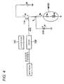
- Fig. 4 is a circuit diagram showing the configuration of a load circuit for driving a motor M101, used for a radiator fan etc. to be mounted on a vehicle, by the PWM control.
- An electronic switch T101 such as a MOSFET is provided between the motor M101 and the positive electrode terminal of a DC power supply VB (for example, a battery to be mounted on the vehicle).
- the inductance of the motor M101 is depicted as LM and an armature resistance thereof is depicted as Ra.
- the gate of the electronic switch T101 is connected to a driver 102 via a resistor R101.
- a charge pump 101 is connected to the driver 102.
- the driver 102 When the driver 102 is supplied with an input signal having a predetermined on/off cycle, the driver 102 outputs the output voltage of the charge pump 101 to the gate of the electronic switch T101 to thereby drive the electronic switch T101 with a predetermined duty ratio according to the PWM control.
- the current ID becomes equal to the current IM in the case where the electronic switch T101 is turned on to flow a current through a path from the positive electrode terminal of the DC power supply VB to the negative electrode terminal of the DC power supply VB via the electronic switch T101, the motor M101 and the ground.
- the electromagnetic energy of LM * IM 2 /2 is accumulated in the inductance LM of the motor M101.
- a flywheel diode D101 (hereinafter simply referred a "diode") is provided in parallel to the motor M101. Supposing that a connection point between the electronic switch T101 and the motor M101 is a, the cathode of the diode D101 is connected to the point a and the anode of the diode D101 is grounded.
- the current IM having been flowing through the motor M101 during the on-state of the electronic switch T101 starts to flow in a circulation manner through a path from the motor M101 to the motor M101 via the ground, the diode D101 and the point a when the electronic switch T101 is turned off.
- the electromagnetic energy having been accumulated in the inductance LM is converted into the driving torque of the motor M101.
- the circulation current IF becomes equal to the current IM.
- a power loss generated in the diode D101 is represented by VF* IF supposing that the voltage drop in the forward direction of the diode D101 is VF. Since this power loss is converted into heat to thereby merely increase the temperature of the diode D101, this power loss does not contribute to the maintaining of the rotation speed of the motor M101.
- This invention has been made in order to solve such the problem of the related art and an object of this invention is to provide a power supply device which can reduce energy loss caused due to the forward direction voltage of a flywheel diode.
- a power supply device comprising:
- the part of the period is set to a period from a time point where a voltage at a first connection point (point a) for connecting between the electronic switch and the motor load reduces to a level equal to or lower than a grounding level after the electronic switch is turned off to a time point before the voltage at the first connection point starts increasing due to disappearance of the electromagnetic energy.
- the semiconductor element includes: a first main electrode which is connected to a first connection point for connecting between the electronic switch and the motor load; a second main electrode which is connected to a ground; and a control electrode to which a control signal is input, the semiconductor element (T2) is turned on when a positive voltage is applied to the control electrode, and the control portion starts applying the positive voltage to the control electrode when the voltage at the first connection point reduces to the level equal to or lower than the grounding level after the electronic switch is shifted to an off state from an on state, and stops application of the positive voltage when a shorter time period has elapsed between a first time period from the application of the positive voltage to a start of increase of the voltage at the first point and a second time period until a constant time period elapses after the application of the positive voltage.
- the semiconductor element (T2) is an N-type field effect transistor which includes a drain as the first main electrode, a source as the second main electrode, and a gate as the control electrode
- the control portion includes a serial connection circuit which is formed by a first resistor (R2) and a transistor (T3), the serial connection circuit is disposed between the DC power supply and the ground, and a control input terminal of the transistor (T3) is connected to the first connection point, a second connection point (point b) for connecting between the first resistor (R2) and the transistor (T3) is connected to the ground via a serial connection circuit formed by a capacitor (C1) and a second resistor (R3), and a third connection point (point c) for connecting between the capacitor (C1) and the second resistor (R3) is connected to a gate of the semiconductor element (T2).
- control portion includes: an inverter circuit which generates an inverted signal of a PWM signal; a delay circuit which delays an output signal of the inverter circuit by a predetermined time, and an one-shot multivibrator which outputs an on-signal with a constant time period in synchronous with a rising timing of the PWM signal as a trigger output from the delay circuit.
- the semiconductor element (T2) such as a MOSFET is provided in parallel to the motor load (M1).
- the semiconductor element (T2) is turned on during a part of the period during which the electronic switch (T1) is placed in the off state.
- a circulation current flowing through the motor load (M1) flows through the semiconductor element (T2).
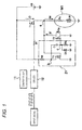
- Fig. 1 is a circuit diagram showing the configuration of a load circuit including a power supply device according to the first embodiment of the invention.
- the load circuit according to this embodiment includes a series connection circuit formed by a DC power supply VB, an electronic switch T1, and a motor M1 (motor load).
- the DC power supply VB is such as a battery to be mounted on a vehicle, for example.
- the electronic switch T1 is such as a MOSFET.
- the motor M1 is used for driving a radiator fan etc.
- the gate of the electronic switch T1 is connected to a driver 12 via a resistor R1.
- the driver 12 is supplied with electric power from a charge pump 11.
- the driver 12 When an input signal having a predetermined on/off cycle is supplied to the driver 12, the driver 12 outputs the output voltage of the charge pump 11 to the gate of the electronic switch T1 to thereby drive the electronic switch T1 with a predetermined duty ratio according to the PWM control.
- the electric power supplied to the motor M1 is controlled, the rotation driving of the motor M1 can be controlled.
- An armature resistance of the motor M1 is depicted as Ra and an inductance of the motor M1 is depicted as LM.
- An N-type MOSFET (T2: semiconductor element) is provided in parallel to the motor M1.
- the drain (first main electrode) of the MOSFET (T2) is connected to a point a (first connection point) which is provided between the electronic switch T1 and the motor M1, and the source (second main electrode) of the MOSFET (T2) is grounded.
- the cathode of the parasitic diode Dp of the MOSFET (T2) is connected to the point a and the anode of the parasitic diode Dp is grounded.
- the gate (control electrode) of the MOSFET (T2) is connected to a control circuit 21, whereby the on/off operation thereof is controlled by the control circuit 21.
- the control circuit 21 includes a transistor T3 (MOSFET in this embodiment), a resistor R2 (first resistor), a resistor R3 (second resistor), a capacitor C1 and a diode D2.
- One end of the resistor R2 is connected to the positive electrode terminal of the DC power supply VB and the other end thereof is grounded via the transistor T3.
- a point b (second connection point) which is provided between the resistor R2 and the transistor T3 is connected to the one end of the capacitor C1.
- the gate of the transistor T3 is connected to the point a.
- a point c which is the other end of the capacitor C1 is connected to the gate of the MOSFET (T2), connected to the ground via the resistor R3 and further connected to cathode of the diode D2.
- the anode of the diode D2 is grounded.
- the control circuit 21 turns the MOSFET (T2) on during a part of a period during which the electronic switch T1 is placed in an off state to thereby reduce an amount of heat generated from the parasitic diode Dp, whereby energy loss can be reduced.
- Figs. 3(a) to 3(e) are timing charts showing waveforms of respective signals of the power supply circuit according to the first embodiment.
- Fig. 3(a) shows the waveform of the input signal supplied to the driver 12
- Fig. 3(b) shows voltage waveforms generated at the point a, point b and point c
- Fig. 3(c) shows the waveform of a current IM flowing through the motor M1
- Fig.3(d) shows the waveform of a current ID flowing through the electronic switch T1
- Fig. 3(e) shows a circulation current IF flowing through the MOSFET (T2) or the parasitic diode Dp.
- Fig. 1 in a state that the electronic switch T1 has not been driven yet, the voltage at the point a is 0V and the transistor T3 is in an off state. Further, since the gate of the MOSFET (T2) is grounded via the resistor R3, the MOSFET (T2) is in an off state.
- the electronic switch T1 repeats on/off states with a predetermined duty ratio. That is, as shown in Fig. 3(a) , the electronic switch T1 repeats the on/off states with a constant period.
- the electronic switch T1 is turned on at a time point t1 shown in Fig. 3(a) , the voltage at the point a increases almost to the output voltage of the DC power supply VB as shown in Fig. 3(b) .
- the current ID flowing through the electronic switch T1 gradually increases as shown in Fig. 3(d) .
- the current IM flowing through the motor M1 gradually increases as shown in Fig. 3(c) .
- the transistor T3 since the gate voltage of the transistor T3 increases, the transistor T3 is turned on to thereby connect the point b to the ground.
- the voltage at the point c which is the gate of the MOSFET (T2) becomes lower than the ground level by the forward direction voltage (hereinafter referred to VF2) of the diode D2, whereby the MOSFET (T2) is turned off. That is, the MOSFET (T2) is turned off when the electronic switch T1 is turned on.
- VF2 forward direction voltage
- the voltage at the point a abruptly reduces in a manner of exceeding the ground level to the negative voltage side as shown in Fig. 3(b) . That is, since the circulation current flows through a path from the motor M1 to the motor M1 via the ground, the parasitic diode Dp and the point a due to the electromagnetic energy having been accumulated in the inductance LM of the motor M1. In this case, the current IM flowing through the motor M1 reduces gradually as shown in Fig. 3(c) , and the circulation current IF same as the current IM flows through the parasitic diode Dp as shown in Fig. 3(e) .
- the parasitic diode Dp of the MOSFET (T2) acts as a flywheel diode.
- the transistor T3 since the transistor T3 is turned off due to the voltage reduction at the point a, the connection between the point b and the ground is interrupted and hence the voltage at the point b increases.
- the voltage at the point c increases in accordance with the increase of the voltage at the point b in a manner that the voltage at the point c is lower than the voltage at the point b by about 0.7 V (see t2 to t3 in Fig. 3 ).
- the MOSFET (T2) is turned on due to the increase of the voltage at the point c, whereby the circulation current IF of the motor M1 stops flowing through the parasitic diode Dp and flows through a path from the motor M1 to the motor M1 via the ground, the MOSFET (T2) and the point a.
- the power loss due to the parasitic diode Dp is replaced by the power loss due to the on-resistance of the MOSFET (T2).
- the on-resistance of the MOSFET (T2) is 5[m ⁇ ] and the circulation current IF is 10A, as an example, the power loss becomes 0.5W.
- the power loss can be 1/14 by using the MOSFET (T2).
- the circulation current becomes the maximum when the electronic switch T1 is turned off and thereafter reduces with a constant rate.
- the power loss abruptly reduces in proportional to the square of the circulation current IF (IF2).
- the MOSFET (T2) since the MOSFET (T2) is turned off at the time point where the electromagnetic energy accumulated in the inductance LM of the motor M1 disappears, the inertial energy of the armature can be prevented from being wasted. Further, the MOSFET (T2) can be surely turned off before a time point t5 where the electronic switch T1 is turned on next.
- the MOSFET (T2) can be turned off before the voltage at the point a increases after the disappearance of the circulation current.
- the MOSFET (T2) can be turned off at the time point before the electromagnetic energy disappears by suitably changing the time constant ⁇ .
- the positive voltage is started to be applied to the gate of the MOSFET (T3) when the electronic switch T1 is shifted to the off state from the on state and the voltage at the point a reduces to the level equal to or lower than the ground level. Then, the application of this positive voltage is stopped to thereby turn the MOSFET (T2) off when a shorter time period has elapsed between a time period (first time period) from the application of this positive voltage to the start of the increase of the voltage at the point a and a time period (second time period) until the constant time period determined by the time constant ⁇ elapses after the application of this positive voltage.
- the circulation current IF flows through the parasitic diode Dp.
- the circulation current IF becomes small after the lapse of the time period determined by the time constant ⁇ , the power loss due to the parasitic diode Dp becomes quite small.
- the MOSFET (T2) is provided in parallel to the motor M1.
- the MOSFET (T2) is turned on during a part of the period during which the electronic switch T1 is placed in the off state.
- the circulation current IF flowing through the motor M1 is circulated via the MOSFET (T2).
- the energy loss can be remarkably reduced as compared with the case of the related art where the circulation current circulates via the flywheel diode.
- the lapsed time period Ty (see Fig. 3(c) ) required until the circulation current disappears is set to be shorter than the turn-off time period Tx of the electronic switch T1 (see Fig. 3(c) ).
- the aforesaid control can be realized so long as the T1 is turned on to thereby increase the voltage at the point a.
- the gate voltage (voltage at the point c) of the MOSFET (T2) is required to become sufficiently small until the electronic switch T1 is turned on. If the gate voltage of the MOSFET (T2) is sufficiently large when the electronic switch T1 is turned on, the current flows through a path from the DC power supply VB to the ground via the electronic switch T1, the point a and the MOSFET (T2), which is the same phenomenon as the case where the load side wiring is short-circuited and grounded. In order to avoid such the phenomenon, it is required to perform such a control of charging the capacitor C1 to reduce the voltage at the point c.
- Fig. 2 is a circuit diagram showing the configuration of a load circuit including a power supply device according to the second embodiment of the invention.
- the power supply device shown in Fig. 2 differs from Fig. 1 in a point that the control portion for controlling the turning-on/off operation of the MOSFET (T2) is changed from the analog circuit to a digital circuit.
- a control circuit 21 a includes an inverter circuit 13 which inverts a PWM signal having a predetermined on/off duty ratio to generate an inverted signal, a delay unit 14 which delays the output signal from the inverter circuit 13 by a predetermined time period (for example 10 [ ⁇ s]), and an one-shot multivibrator 15 which outputs an on-signal of a constant time period (Tz) in synchronous with the rising timing of the PWM signal as a trigger output from the delay unit 14.
- the output signal of the one-shot multivibrator 15 is supplied to the gate of the MOSFET (T2).
- the one-shot multivibrator 15 outputs to the gate of the MOSFET (T2), as the output signal, a signal of "H" level with the constant time period Tz upon the lapse of 10[ ⁇ s] after the input signal supplied to the driver 12 is interrupted.
- the constant time period Tz is set to be shorter than each of the time period Tx and the time period Ty shown in Fig. 3 .
- the MOSFET (T2) can be turned on during a part of the time period during which the electronic switch T1 is placed in the off state to thereby flow the circulation current via the MOSFET (T2).
- the circulation current IF still exists after the lapse of a time period of (Tz +10 [ ⁇ s]) after the turning-off of the electronic switch T1
- the circulation current flows through the parasitic diode Dp.
- control circuit 21a is configured by the digital circuit including the one-shot multivibrator 15, it is possible to obtain an effect that the circuit can be designed by the easier method in addition to the aforesaid effects described in the first embodiment.
- the invention is not limited thereto and may be applied to a case of driving the load of the motor under the PWM control by using the DC power supply.
- This invention is quite useful since the energy loss can be reduced at the time of driving the motor by using the PWM control.
Landscapes
- Engineering & Computer Science (AREA)
- Power Engineering (AREA)
- Control Of Direct Current Motors (AREA)
- Dc-Dc Converters (AREA)
- Electronic Switches (AREA)
Abstract
Description
- The present invention relates to a power supply device for controlling an electric power supplied to a motor load by PWM controlling an electronic switch with a desired duty ratio and, in particular, relates to a technique of reducing energy loss due to heat generation.
- Many load circuits have been employed each of which is configured in a manner that an electronic switch such as a MOSFET is provided between a DC power supply and a load, and the MOSFET is subjected to the PWM control to adjust an electric power supplied to the load to thereby control the output of the load (see a
patent document 1, for example). -
Fig. 4 is a circuit diagram showing the configuration of a load circuit for driving a motor M101, used for a radiator fan etc. to be mounted on a vehicle, by the PWM control. An electronic switch T101 such as a MOSFET is provided between the motor M101 and the positive electrode terminal of a DC power supply VB (for example, a battery to be mounted on the vehicle). The inductance of the motor M101 is depicted as LM and an armature resistance thereof is depicted as Ra. - The gate of the electronic switch T101 is connected to a
driver 102 via a resistor R101. Acharge pump 101 is connected to thedriver 102. When thedriver 102 is supplied with an input signal having a predetermined on/off cycle, thedriver 102 outputs the output voltage of thecharge pump 101 to the gate of the electronic switch T101 to thereby drive the electronic switch T101 with a predetermined duty ratio according to the PWM control. - As shown in
Fig. 4 , supposing that a current flowing through the electronic switch T101 is ID and a current flowing through the motor M101 is IM, the current ID becomes equal to the current IM in the case where the electronic switch T101 is turned on to flow a current through a path from the positive electrode terminal of the DC power supply VB to the negative electrode terminal of the DC power supply VB via the electronic switch T101, the motor M101 and the ground. In this case, the electromagnetic energy of LM * IM2/2 is accumulated in the inductance LM of the motor M101. - When the electronic switch T101 is turned off, the current ID becomes 0. However, the current IM tends to continuously flow due to the inductance LM of the motor M101. In order to flow this current into the motor M101 in a circulation manner, a flywheel diode D101 (hereinafter simply referred a "diode") is provided in parallel to the motor M101. Supposing that a connection point between the electronic switch T101 and the motor M101 is a, the cathode of the diode D101 is connected to the point a and the anode of the diode D101 is grounded.
- According to this configuration, the current IM having been flowing through the motor M101 during the on-state of the electronic switch T101 starts to flow in a circulation manner through a path from the motor M101 to the motor M101 via the ground, the diode D101 and the point a when the electronic switch T101 is turned off. Thus, the electromagnetic energy having been accumulated in the inductance LM is converted into the driving torque of the motor M101. In this case, supposing that the current flowing through the diode D101 is a circulation current IF, the circulation current IF becomes equal to the current IM.
- The motor current IM (= IF) flows through the armature resistor Ra and the diode D101 to thereby cause a power loss.
- Since the power loss at the armature resistor Ra causes the generation of the motor driving torque, this power loss has an effects of suppressing the reduction of the rotation speed of the motor M101 during the off period of the electronic switch T101. On the other hand, a power loss generated in the diode D101 is represented by VF* IF supposing that the voltage drop in the forward direction of the diode D101 is VF. Since this power loss is converted into heat to thereby merely increase the temperature of the diode D101, this power loss does not contribute to the maintaining of the rotation speed of the motor M101.
- When the electromagnetic energy accumulated in the inductance LM of the motor M101 disappears as the power loss of the armature resistor Ra and the diode D101, the voltage at the point a increases to the generation voltage due to the inertial force of the motor armature. In this case, the diode D101 prevents a current from flowing toward the ground from the point a.
- That is, a part of the electromagnetic energy accumulated in the inductance LM is converted into the torque of the motor M101 and the remaining of the electromagnetic energy is converted into heat generated by the diode D101. Thus, if it becomes possible to reduce the power loss of the diode D101, the conversion ratio into the torque of the motor M101 can be increased, whereby the energy can be utilized effectively and an amount of heat generated from the diode D101 can be reduced.
-
- Patent literature 1:
JP-A-11-168899 - As described above, in the load circuit of the related art, in the case of PMC controlling the motor M101 by using the electronic switch T101, when the electronic switch T101 is changed to the off state from the on state, the current IM generated by the electromagnetic energy accumulated in the inductance LM is flown into the motor M101 in the circulation manner via the flywheel diode D101. However, in the case of employing this system, the flywheel diode D101 generates heat, and hence the energy loss is generated due to the heat. Thus, it has been increasingly demanded to reduce such the energy loss.
- This invention has been made in order to solve such the problem of the related art and an object of this invention is to provide a power supply device which can reduce energy loss caused due to the forward direction voltage of a flywheel diode.
- In order to achieve the above object, according to the present invention, there is provided a power supply device, comprising:
- an electronic switch (T1) provided on a wiring which connects a DC power supply (VB) to a motor load (M1);
- a driving portion that controls the electronic switch with PWM to drive the motor load;
- a semiconductor element (T2) that has a parasitic diode and is disposed in parallel to the motor load so that a forward direction of the parasitic diode is in opposite to a flowing direction of a current flowing through the motor load; and
- a control portion that controls the semiconductor element so as to be turned on during a part of a period during which the electronic switch is placed in an off state under a control with the PWM.
- Preferably, in a case where electromagnetic energy accumulated in an inductance of the motor load disappears until the electronic switch is turned on again after the electronic switch is turned off, the part of the period is set to a period from a time point where a voltage at a first connection point (point a) for connecting between the electronic switch and the motor load reduces to a level equal to or lower than a grounding level after the electronic switch is turned off to a time point before the voltage at the first connection point starts increasing due to disappearance of the electromagnetic energy.
- Preferably, the semiconductor element includes: a first main electrode which is connected to a first connection point for connecting between the electronic switch and the motor load; a second main electrode which is connected to a ground; and a control electrode to which a control signal is input, the semiconductor element (T2) is turned on when a positive voltage is applied to the control electrode, and the control portion starts applying the positive voltage to the control electrode when the voltage at the first connection point reduces to the level equal to or lower than the grounding level after the electronic switch is shifted to an off state from an on state, and stops application of the positive voltage when a shorter time period has elapsed between a first time period from the application of the positive voltage to a start of increase of the voltage at the first point and a second time period until a constant time period elapses after the application of the positive voltage.
- Preferably, the semiconductor element (T2) is an N-type field effect transistor which includes a drain as the first main electrode, a source as the second main electrode, and a gate as the control electrode, the control portion includes a serial connection circuit which is formed by a first resistor (R2) and a transistor (T3), the serial connection circuit is disposed between the DC power supply and the ground, and a control input terminal of the transistor (T3) is connected to the first connection point, a second connection point (point b) for connecting between the first resistor (R2) and the transistor (T3) is connected to the ground via a serial connection circuit formed by a capacitor (C1) and a second resistor (R3), and a third connection point (point c) for connecting between the capacitor (C1) and the second resistor (R3) is connected to a gate of the semiconductor element (T2).
- Preferably, the control portion includes: an inverter circuit which generates an inverted signal of a PWM signal; a delay circuit which delays an output signal of the inverter circuit by a predetermined time, and an one-shot multivibrator which outputs an on-signal with a constant time period in synchronous with a rising timing of the PWM signal as a trigger output from the delay circuit.
- In the power supply device according to the invention, the semiconductor element (T2) such as a MOSFET is provided in parallel to the motor load (M1). At the time of driving the motor load by subjecting the electronic switch (T1) to the PWM control, the semiconductor element (T2) is turned on during a part of the period during which the electronic switch (T1) is placed in the off state. Thus, a circulation current flowing through the motor load (M1) flows through the semiconductor element (T2). As a result, since an amount of heat generation can be reduced as compared with the case of the related art where the flywheel diode is employed, the energy loss can be reduced.
-
- [
Fig. 1 ] A circuit diagram showing the configuration of a load circuit including a power supply device according to the first embodiment of the invention. - [
Fig. 2 ] A circuit diagram showing the configuration of a load circuit including a power supply device according to the second embodiment of the invention. - [
Fig. 3 ] (a) to (e) are timing charts showing respective waveforms of the load circuit including the power supply device according to the embodiment of the invention. - [
Fig. 4 ] A circuit diagram showing the configuration of a load circuit including a power supply device of a related art. - Hereinafter, embodiments according to the invention will be explained with reference to drawings.
Fig. 1 is a circuit diagram showing the configuration of a load circuit including a power supply device according to the first embodiment of the invention. As shown inFig. 1 , the load circuit according to this embodiment includes a series connection circuit formed by a DC power supply VB, an electronic switch T1, and a motor M1 (motor load). The DC power supply VB is such as a battery to be mounted on a vehicle, for example. The electronic switch T1 is such as a MOSFET. The motor M1 is used for driving a radiator fan etc. The gate of the electronic switch T1 is connected to adriver 12 via a resistor R1. Thedriver 12 is supplied with electric power from acharge pump 11. - When an input signal having a predetermined on/off cycle is supplied to the
driver 12, thedriver 12 outputs the output voltage of thecharge pump 11 to the gate of the electronic switch T1 to thereby drive the electronic switch T1 with a predetermined duty ratio according to the PWM control. As a result, since the electric power supplied to the motor M1 is controlled, the rotation driving of the motor M1 can be controlled. An armature resistance of the motor M1 is depicted as Ra and an inductance of the motor M1 is depicted as LM. - An N-type MOSFET (T2: semiconductor element) is provided in parallel to the motor M1. The drain (first main electrode) of the MOSFET (T2) is connected to a point a (first connection point) which is provided between the electronic switch T1 and the motor M1, and the source (second main electrode) of the MOSFET (T2) is grounded. The cathode of the parasitic diode Dp of the MOSFET (T2) is connected to the point a and the anode of the parasitic diode Dp is grounded.
- The gate (control electrode) of the MOSFET (T2) is connected to a
control circuit 21, whereby the on/off operation thereof is controlled by thecontrol circuit 21. - The
control circuit 21 includes a transistor T3 (MOSFET in this embodiment), a resistor R2 (first resistor), a resistor R3 (second resistor), a capacitor C1 and a diode D2. - One end of the resistor R2 is connected to the positive electrode terminal of the DC power supply VB and the other end thereof is grounded via the transistor T3. A point b (second connection point) which is provided between the resistor R2 and the transistor T3 is connected to the one end of the capacitor C1. The gate of the transistor T3 is connected to the point a.
- A point c (third connection point) which is the other end of the capacitor C1 is connected to the gate of the MOSFET (T2), connected to the ground via the resistor R3 and further connected to cathode of the diode D2. The anode of the diode D2 is grounded.
- The
control circuit 21 turns the MOSFET (T2) on during a part of a period during which the electronic switch T1 is placed in an off state to thereby reduce an amount of heat generated from the parasitic diode Dp, whereby energy loss can be reduced. - Hereinafter, the explanation will be made as to the operation of the power supply circuit according to the first embodiment.
Figs. 3(a) to 3(e) are timing charts showing waveforms of respective signals of the power supply circuit according to the first embodiment.Fig. 3(a) shows the waveform of the input signal supplied to thedriver 12,Fig. 3(b) shows voltage waveforms generated at the point a, point b and point c,Fig. 3(c) shows the waveform of a current IM flowing through the motor M1,Fig.3(d) shows the waveform of a current ID flowing through the electronic switch T1, andFig. 3(e) shows a circulation current IF flowing through the MOSFET (T2) or the parasitic diode Dp. - In
Fig. 1 , in a state that the electronic switch T1 has not been driven yet, the voltage at the point a is 0V and the transistor T3 is in an off state. Further, since the gate of the MOSFET (T2) is grounded via the resistor R3, the MOSFET (T2) is in an off state. - When the
driver 12 outputs a PWM signal to thereby supply a driving signal to the gate of the electronic switch T1, the electronic switch T1 repeats on/off states with a predetermined duty ratio. That is, as shown inFig. 3(a) , the electronic switch T1 repeats the on/off states with a constant period. When the electronic switch T1 is turned on at a time point t1 shown inFig. 3(a) , the voltage at the point a increases almost to the output voltage of the DC power supply VB as shown inFig. 3(b) . Further, the current ID flowing through the electronic switch T1 gradually increases as shown inFig. 3(d) . Similarly, the current IM flowing through the motor M1 gradually increases as shown inFig. 3(c) . - As a result, since the gate voltage of the transistor T3 increases, the transistor T3 is turned on to thereby connect the point b to the ground. Thus, the voltage at the point c which is the gate of the MOSFET (T2) becomes lower than the ground level by the forward direction voltage (hereinafter referred to VF2) of the diode D2, whereby the MOSFET (T2) is turned off. That is, the MOSFET (T2) is turned off when the electronic switch T1 is turned on.
- Next, when the electronic switch T1 is turned off at a time point t2 shown in
Fig. 3(a) , the voltage at the point a abruptly reduces in a manner of exceeding the ground level to the negative voltage side as shown inFig. 3(b) . That is, since the circulation current flows through a path from the motor M1 to the motor M1 via the ground, the parasitic diode Dp and the point a due to the electromagnetic energy having been accumulated in the inductance LM of the motor M1. In this case, the current IM flowing through the motor M1 reduces gradually as shown inFig. 3(c) , and the circulation current IF same as the current IM flows through the parasitic diode Dp as shown inFig. 3(e) . - When the voltage at the point a reduces to a level lower than the ground level by about 0.7 V to 1 V, the voltage at the point a is clamped by the parasitic diode Dp of the MOSFET (T2) and hence prevented from being reduced any more (see a symbol q1 of
Fig. 3(b) ). That is, the parasitic diode Dp acts as a flywheel diode. - Then, since the transistor T3 is turned off due to the voltage reduction at the point a, the connection between the point b and the ground is interrupted and hence the voltage at the point b increases. The voltage at the point c increases in accordance with the increase of the voltage at the point b in a manner that the voltage at the point c is lower than the voltage at the point b by about 0.7 V (see t2 to t3 in
Fig. 3 ). - The MOSFET (T2) is turned on due to the increase of the voltage at the point c, whereby the circulation current IF of the motor M1 stops flowing through the parasitic diode Dp and flows through a path from the motor M1 to the motor M1 via the ground, the MOSFET (T2) and the point a. Thus, the power loss due to the parasitic diode Dp is replaced by the power loss due to the on-resistance of the MOSFET (T2). Supposing that the on-resistance of the MOSFET (T2) is 5[mΩ] and the circulation current IF is 10A, as an example, the power loss becomes 0.5W.
- In contrast, supposing that the voltage drop in the forward direction of the parasitic diode Dp is 0.7V, since the power loss becomes 7W when the circulation current of 10A flows, the power loss can be 1/14 by using the MOSFET (T2). The circulation current becomes the maximum when the electronic switch T1 is turned off and thereafter reduces with a constant rate. Thus, the power loss abruptly reduces in proportional to the square of the circulation current IF (IF2).
- When the circulation current IF disappears at a time point t4 (see
Fig. 3(b) ) upon the lapse of a time period Ty after the time point t2 where the electronic switch T1 is turned off, the motor M1 generates the power by the rotation due to the inertial force of the armature to thereby increases the voltage at the point a (see a symbol q2 inFig. 3(b) ). The transistor T3 is turned on due to the voltage increase at the point a, whereby since the voltage at the point c becomes equal to or lower than the ground level, the MOSFET (T2) is turned off. Thus, the current path from the point a to the ground via the MOSFET (T2) is interrupted. In other words, since the MOSFET (T2) is turned off at the time point where the electromagnetic energy accumulated in the inductance LM of the motor M1 disappears, the inertial energy of the armature can be prevented from being wasted. Further, the MOSFET (T2) can be surely turned off before a time point t5 where the electronic switch T1 is turned on next. - Further, although the voltage at the point c is raised in accordance with the increase of the voltage at the point b immediately after the turning-off of the electronic switch T1 (see t2 to t3 in
Fig. 3 ), since the capacitor C1 is charged by a current flowing through a path from the DC power supply VB to the ground via the resistor R2, the capacitor C1 and the resistor R3, the voltage at the point c reduces with the time lapse (see t3 to t4 inFig. 3 ). In this case, a time constant τ of the current charging the capacitor C1 becomes τ= C1* (R2 + R3). Thus, when the time constant τ is set to a small value, the MOSFET (T2) can be turned off before the voltage at the point a increases after the disappearance of the circulation current. In other words, the MOSFET (T2) can be turned off at the time point before the electromagnetic energy disappears by suitably changing the time constant τ. - That is, according to the invention, the positive voltage is started to be applied to the gate of the MOSFET (T3) when the electronic switch T1 is shifted to the off state from the on state and the voltage at the point a reduces to the level equal to or lower than the ground level. Then, the application of this positive voltage is stopped to thereby turn the MOSFET (T2) off when a shorter time period has elapsed between a time period (first time period) from the application of this positive voltage to the start of the increase of the voltage at the point a and a time period (second time period) until the constant time period determined by the time constant τ elapses after the application of this positive voltage.
- After the turning-off of the MOSFET (T2), the circulation current IF flows through the parasitic diode Dp. In this case, although there is a fear about the power loss due to the parasitic diode Dp, since the circulation current IF becomes small after the lapse of the time period determined by the time constant τ, the power loss due to the parasitic diode Dp becomes quite small.
- In this manner, according to the power supply device of the first embodiment, the MOSFET (T2) is provided in parallel to the motor M1. At the time of driving the electronic switch T1 by the PWM control to thereby supply the power to the motor M1, the MOSFET (T2) is turned on during a part of the period during which the electronic switch T1 is placed in the off state. Thus, when the electronic switch T1 is placed in the off state, the circulation current IF flowing through the motor M1 is circulated via the MOSFET (T2). As a result, the energy loss can be remarkably reduced as compared with the case of the related art where the circulation current circulates via the flywheel diode.
- Further, at the time of executing the PWM control, since the MOSFET (T2) is turned on after the electronic switch T1 is turned off and the MOSFET (T2) is turned off before the electronic switch T1 is turned on, such a phenomenon can be surely prevented from occurring that both the MOSFET (T2) and the electronic switch T1 are simultaneously turned on.
- In the aforesaid first embodiment, the lapsed time period Ty (see
Fig. 3(c) ) required until the circulation current disappears is set to be shorter than the turn-off time period Tx of the electronic switch T1 (seeFig. 3(c) ). However, even if the time period Tx becomes equal to or smaller than the time period Ty, the aforesaid control can be realized so long as the T1 is turned on to thereby increase the voltage at the point a. - In order to realize such the control, the gate voltage (voltage at the point c) of the MOSFET (T2) is required to become sufficiently small until the electronic switch T1 is turned on. If the gate voltage of the MOSFET (T2) is sufficiently large when the electronic switch T1 is turned on, the current flows through a path from the DC power supply VB to the ground via the electronic switch T1, the point a and the MOSFET (T2), which is the same phenomenon as the case where the load side wiring is short-circuited and grounded. In order to avoid such the phenomenon, it is required to perform such a control of charging the capacitor C1 to reduce the voltage at the point c.
- Next, the second embodiment of this invention will be explained.
Fig. 2 is a circuit diagram showing the configuration of a load circuit including a power supply device according to the second embodiment of the invention. The power supply device shown inFig. 2 differs fromFig. 1 in a point that the control portion for controlling the turning-on/off operation of the MOSFET (T2) is changed from the analog circuit to a digital circuit. - A
control circuit 21 a according to the second embodiment includes aninverter circuit 13 which inverts a PWM signal having a predetermined on/off duty ratio to generate an inverted signal, adelay unit 14 which delays the output signal from theinverter circuit 13 by a predetermined time period (for example 10 [µs]), and an one-shot multivibrator 15 which outputs an on-signal of a constant time period (Tz) in synchronous with the rising timing of the PWM signal as a trigger output from thedelay unit 14. The output signal of the one-shot multivibrator 15 is supplied to the gate of the MOSFET (T2). - Thus, the one-
shot multivibrator 15 outputs to the gate of the MOSFET (T2), as the output signal, a signal of "H" level with the constant time period Tz upon the lapse of 10[µs] after the input signal supplied to thedriver 12 is interrupted. - In this case, the constant time period Tz is set to be shorter than each of the time period Tx and the time period Ty shown in
Fig. 3 . Thus, the MOSFET (T2) can be turned on during a part of the time period during which the electronic switch T1 is placed in the off state to thereby flow the circulation current via the MOSFET (T2). In the case where the circulation current IF still exists after the lapse of a time period of (Tz +10 [µs]) after the turning-off of the electronic switch T1, the circulation current flows through the parasitic diode Dp. - In this manner, according to the power supply device of the second embodiment, since the
control circuit 21a is configured by the digital circuit including the one-shot multivibrator 15, it is possible to obtain an effect that the circuit can be designed by the easier method in addition to the aforesaid effects described in the first embodiment. - Although the explanation is made as to the power supply device according to the invention based on the embodiments shown in the drawings, the invention is not limited thereto and the configuration of each of the respective portions may be replaced by an arbitrary configuration having the similar function.
- For example, although the aforesaid embodiments are explained as to the case of driving the radiator fan to be mounted on a vehicle as an example, the invention is not limited thereto and may be applied to a case of driving the load of the motor under the PWM control by using the DC power supply.
- Although the invention is explained in detail with reference to the particular embodiments, it will be apparent for those skilled in the art that various changes and modifications are possible without departing from the spirit , range or intentional range of the invention.
This invention is based on Japanese Patent Application (Japanese Patent Application No.2008-329693) filed on December 25, 2008 - This invention is quite useful since the energy loss can be reduced at the time of driving the motor by using the PWM control.
-
- 11
- charge pump
- 12
- driver
- 13
- inverter circuit
- 14
- delay unit
- 15
- one-shot multivibrator
- 21, 21a
- control circuit (control portion)
- VB
- DC power supply
- T1
- electronic switch
- T2
- MOSFET (semiconductor element)
- T3
- transistor
- Dp
- parasitic diode
- D2
- diode
- C1
- capacitor
- R1
- resistor
- R2
- resistor (first resistor)
- R3
- resistor (second resistor)
- M1
- motor (motor load)
- Ra
- armature resistor
- LM
- inductance
Claims (5)
- A power supply device, comprising:an electronic switch provided on a wiring which connects a DC power supply to a motor load;a driving portion that controls the electronic switch with PWM to drive the motor load;a semiconductor element that has a parasitic diode and is disposed in parallel to the motor load so that a forward direction of the parasitic diode is in opposite to a flowing direction of a current flowing through the motor load; anda control portion that controls the semiconductor element so as to be turned on during a part of a period during which the electronic switch is placed in an off state under a control with the PWM.
- The power supply device according to claim 1, wherein in a case where electromagnetic energy accumulated in an inductance of the motor load disappears until the electronic switch is turned on again after the electronic switch is turned off, the part of the period is set to a period from a time point where a voltage at a first connection point for connecting between the electronic switch and the motor load reduces to a level equal to or lower than a grounding level after the electronic switch is turned off to a time point before the voltage at the first connection point starts increasing due to disappearance of the electromagnetic energy.
- The power supply device according to claim 1, wherein the semiconductor element includes:a first main electrode which is connected to a first connection point for connecting between the electronic switch and the motor load;a second main electrode which is connected to a ground; anda control electrode to which a control signal is input,wherein the semiconductor element is turned on when a positive voltage is applied to the control electrode; and
wherein the control portion starts applying the positive voltage to the control electrode when the voltage at the first connection point reduces to the level equal to or lower than the grounding level after the electronic switch is shifted to an off state from an on state, and stops application of the positive voltage when a shorter time period has elapsed between a first time period from the application of the positive voltage to a start of increase of the voltage at the first point and a second time period until a constant time period elapses after the application of the positive voltage. - The power supply device according to any one of claims 1 to 3, wherein the semiconductor element is an N-type field effect transistor which includes a drain as the first main electrode, a source as the second main electrode, and a gate as the control electrode;
wherein the control portion includes a serial connection circuit which is formed by a first resistor and a transistor;
wherein the serial connection circuit is disposed between the DC power supply and the ground; and
wherein a control input terminal of the transistor is connected to the first connection point, a second connection point for connecting between the first resistor and the transistor is connected to the ground via a serial connection circuit formed by a capacitor and a second resistor, and a third connection point for connecting between the capacitor and the second resistor is connected to a gate of the semiconductor element. - The power supply device according to claim 1, wherein the control portion includes:an inverter circuit which generates an inverted signal of a PWM signal;a delay circuit which delays an output signal of the inverter circuit by a predetermined time; andan one-shot multivibrator which outputs an on-signal with a constant time period in synchronous with a rising timing of the PWM signal as a trigger output from the delay circuit.
Applications Claiming Priority (2)
| Application Number | Priority Date | Filing Date | Title |
|---|---|---|---|
| JP2008329693A JP5303262B2 (en) | 2008-12-25 | 2008-12-25 | Power supply |
| PCT/JP2009/071491 WO2010074176A1 (en) | 2008-12-25 | 2009-12-24 | Power supply device |
Publications (3)
| Publication Number | Publication Date |
|---|---|
| EP2372898A1 true EP2372898A1 (en) | 2011-10-05 |
| EP2372898A4 EP2372898A4 (en) | 2017-11-22 |
| EP2372898B1 EP2372898B1 (en) | 2020-07-15 |
Family
ID=42287783
Family Applications (1)
| Application Number | Title | Priority Date | Filing Date |
|---|---|---|---|
| EP09834974.9A Active EP2372898B1 (en) | 2008-12-25 | 2009-12-24 | Power supply device |
Country Status (5)
| Country | Link |
|---|---|
| US (1) | US8536819B2 (en) |
| EP (1) | EP2372898B1 (en) |
| JP (1) | JP5303262B2 (en) |
| CN (1) | CN102265501B (en) |
| WO (1) | WO2010074176A1 (en) |
Families Citing this family (8)
| Publication number | Priority date | Publication date | Assignee | Title |
|---|---|---|---|---|
| TW201225510A (en) * | 2010-12-07 | 2012-06-16 | xiang-yu Li | Safe motor energy recycling device |
| CN102570947A (en) * | 2011-12-05 | 2012-07-11 | 江苏浩峰汽车附件有限公司 | Switch control speed regulating circuit of direct current motor with braking function |
| CN102739144B (en) * | 2012-06-29 | 2015-07-22 | 深圳市航盛电子股份有限公司 | Belt-starter generator (BSG) motor control system for micro hybrid vehicle |
| CN104569857A (en) * | 2015-01-21 | 2015-04-29 | 浪潮电子信息产业股份有限公司 | A Design Method and Test Tool for Substituting Load Meter |
| WO2016167185A1 (en) * | 2015-04-17 | 2016-10-20 | 日立オートモティブシステムズ株式会社 | In-vehicle control device |
| CN104953902B (en) * | 2015-06-11 | 2018-06-19 | 南京普天大唐信息电子有限公司 | A kind of switched reluctance machines power control circuit |
| US10868525B2 (en) * | 2018-11-13 | 2020-12-15 | Mohammad GH. Alijani | Power transmission through a single conductive element |
| JP7596736B2 (en) | 2020-11-17 | 2024-12-10 | 株式会社オートネットワーク技術研究所 | Power supply control device, power supply control method, and computer program |
Family Cites Families (8)
| Publication number | Priority date | Publication date | Assignee | Title |
|---|---|---|---|---|
| JP2806929B2 (en) * | 1987-09-29 | 1998-09-30 | 株式会社デンソー | Motor drive control device |
| JPH11168899A (en) * | 1997-12-01 | 1999-06-22 | Zexel:Kk | Drive control method and apparatus in motor drive controller |
| JP2000201475A (en) * | 1999-01-04 | 2000-07-18 | Texas Instr Japan Ltd | Power supply |
| JP3626114B2 (en) * | 2001-06-06 | 2005-03-02 | 株式会社デンソー | DC-DC converter |
| JP3494223B2 (en) * | 2001-12-03 | 2004-02-09 | サンケン電気株式会社 | DC-DC converter |
| JP2005158870A (en) | 2003-11-21 | 2005-06-16 | Fujitsu Ten Ltd | Load controller |
| DE502005005617D1 (en) * | 2005-06-01 | 2008-11-20 | Metabowerke Gmbh | Control device for a DC electric motor of a power tool device |
| JP2008099474A (en) | 2006-10-13 | 2008-04-24 | Advics:Kk | Electric motor drive circuit for vehicle |
-
2008
- 2008-12-25 JP JP2008329693A patent/JP5303262B2/en not_active Expired - Fee Related
-
2009
- 2009-12-24 US US13/129,441 patent/US8536819B2/en not_active Expired - Fee Related
- 2009-12-24 EP EP09834974.9A patent/EP2372898B1/en active Active
- 2009-12-24 WO PCT/JP2009/071491 patent/WO2010074176A1/en not_active Ceased
- 2009-12-24 CN CN200980152850.0A patent/CN102265501B/en not_active Expired - Fee Related
Non-Patent Citations (1)
| Title |
|---|
| See references of WO2010074176A1 * |
Also Published As
| Publication number | Publication date |
|---|---|
| WO2010074176A1 (en) | 2010-07-01 |
| US8536819B2 (en) | 2013-09-17 |
| CN102265501B (en) | 2014-08-20 |
| JP2010154647A (en) | 2010-07-08 |
| EP2372898A4 (en) | 2017-11-22 |
| US20110221376A1 (en) | 2011-09-15 |
| CN102265501A (en) | 2011-11-30 |
| JP5303262B2 (en) | 2013-10-02 |
| EP2372898B1 (en) | 2020-07-15 |
Similar Documents
| Publication | Publication Date | Title |
|---|---|---|
| US8536819B2 (en) | Power supply device | |
| US7692474B2 (en) | Control circuit for a high-side semiconductor switch for switching a supply voltage | |
| US9240739B2 (en) | Driving system for driving switching element | |
| CN205725692U (en) | For driving the gate driver circuit of power switch | |
| US20140307495A1 (en) | Driver for target switching element and control system for machine using the same | |
| CN104866000B (en) | Gate drive circuit and method with voltage regulator | |
| EP2246971A1 (en) | Motor load control device | |
| CN107769554B (en) | Control circuit of switching power supply device and switching power supply device | |
| JP2905459B2 (en) | Buck regulator circuit | |
| US10931278B2 (en) | Driving circuit of switching transistor | |
| JP2022135911A (en) | Bipolar pulse voltage gate driver | |
| JP5447575B2 (en) | Drive device | |
| US9812944B2 (en) | Discharge device | |
| CN112104204B (en) | Apparatus and method for controlling driving of switching device of power converter | |
| US20070127276A1 (en) | Power supply and display | |
| KR100453666B1 (en) | Voltage controller for automotive alternator | |
| JP2001069667A (en) | Vehicle lamp lighting drive device | |
| JP2009095214A (en) | DC-DC converter circuit | |
| US20170063365A1 (en) | Method and Drive Circuit for Driving a Transistor | |
| EP4216436A1 (en) | Charge redistribution for powering a driven switch | |
| CN103715888B (en) | Method for reducing power loss in circuits driving inductive loads | |
| US8638129B2 (en) | Power circuit | |
| US11990826B2 (en) | Power electronics device and method for supplying electrical voltage to a driver circuit of a power semiconductor switch | |
| JP2018093638A (en) | Protection circuit, and motor unit | |
| JP2806929B2 (en) | Motor drive control device |
Legal Events
| Date | Code | Title | Description |
|---|---|---|---|
| PUAI | Public reference made under article 153(3) epc to a published international application that has entered the european phase |
Free format text: ORIGINAL CODE: 0009012 |
|
| 17P | Request for examination filed |
Effective date: 20110615 |
|
| AK | Designated contracting states |
Kind code of ref document: A1 Designated state(s): AT BE BG CH CY CZ DE DK EE ES FI FR GB GR HR HU IE IS IT LI LT LU LV MC MK MT NL NO PL PT RO SE SI SK SM TR |
|
| DAX | Request for extension of the european patent (deleted) | ||
| RA4 | Supplementary search report drawn up and despatched (corrected) |
Effective date: 20171019 |
|
| RIC1 | Information provided on ipc code assigned before grant |
Ipc: H02P 7/29 20160101AFI20171013BHEP |
|
| GRAP | Despatch of communication of intention to grant a patent |
Free format text: ORIGINAL CODE: EPIDOSNIGR1 |
|
| STAA | Information on the status of an ep patent application or granted ep patent |
Free format text: STATUS: GRANT OF PATENT IS INTENDED |
|
| INTG | Intention to grant announced |
Effective date: 20200424 |
|
| GRAS | Grant fee paid |
Free format text: ORIGINAL CODE: EPIDOSNIGR3 |
|
| GRAA | (expected) grant |
Free format text: ORIGINAL CODE: 0009210 |
|
| STAA | Information on the status of an ep patent application or granted ep patent |
Free format text: STATUS: THE PATENT HAS BEEN GRANTED |
|
| AK | Designated contracting states |
Kind code of ref document: B1 Designated state(s): AT BE BG CH CY CZ DE DK EE ES FI FR GB GR HR HU IE IS IT LI LT LU LV MC MK MT NL NO PL PT RO SE SI SK SM TR |
|
| REG | Reference to a national code |
Ref country code: GB Ref legal event code: FG4D Ref country code: CH Ref legal event code: EP |
|
| REG | Reference to a national code |
Ref country code: DE Ref legal event code: R096 Ref document number: 602009062438 Country of ref document: DE |
|
| REG | Reference to a national code |
Ref country code: IE Ref legal event code: FG4D |
|
| REG | Reference to a national code |
Ref country code: AT Ref legal event code: REF Ref document number: 1292093 Country of ref document: AT Kind code of ref document: T Effective date: 20200815 |
|
| REG | Reference to a national code |
Ref country code: LT Ref legal event code: MG4D |
|
| REG | Reference to a national code |
Ref country code: AT Ref legal event code: MK05 Ref document number: 1292093 Country of ref document: AT Kind code of ref document: T Effective date: 20200715 |
|
| REG | Reference to a national code |
Ref country code: NL Ref legal event code: MP Effective date: 20200715 |
|
| PG25 | Lapsed in a contracting state [announced via postgrant information from national office to epo] |
Ref country code: LT Free format text: LAPSE BECAUSE OF FAILURE TO SUBMIT A TRANSLATION OF THE DESCRIPTION OR TO PAY THE FEE WITHIN THE PRESCRIBED TIME-LIMIT Effective date: 20200715 Ref country code: ES Free format text: LAPSE BECAUSE OF FAILURE TO SUBMIT A TRANSLATION OF THE DESCRIPTION OR TO PAY THE FEE WITHIN THE PRESCRIBED TIME-LIMIT Effective date: 20200715 Ref country code: BG Free format text: LAPSE BECAUSE OF FAILURE TO SUBMIT A TRANSLATION OF THE DESCRIPTION OR TO PAY THE FEE WITHIN THE PRESCRIBED TIME-LIMIT Effective date: 20201015 Ref country code: PT Free format text: LAPSE BECAUSE OF FAILURE TO SUBMIT A TRANSLATION OF THE DESCRIPTION OR TO PAY THE FEE WITHIN THE PRESCRIBED TIME-LIMIT Effective date: 20201116 Ref country code: HR Free format text: LAPSE BECAUSE OF FAILURE TO SUBMIT A TRANSLATION OF THE DESCRIPTION OR TO PAY THE FEE WITHIN THE PRESCRIBED TIME-LIMIT Effective date: 20200715 Ref country code: GR Free format text: LAPSE BECAUSE OF FAILURE TO SUBMIT A TRANSLATION OF THE DESCRIPTION OR TO PAY THE FEE WITHIN THE PRESCRIBED TIME-LIMIT Effective date: 20201016 Ref country code: NO Free format text: LAPSE BECAUSE OF FAILURE TO SUBMIT A TRANSLATION OF THE DESCRIPTION OR TO PAY THE FEE WITHIN THE PRESCRIBED TIME-LIMIT Effective date: 20201015 Ref country code: FI Free format text: LAPSE BECAUSE OF FAILURE TO SUBMIT A TRANSLATION OF THE DESCRIPTION OR TO PAY THE FEE WITHIN THE PRESCRIBED TIME-LIMIT Effective date: 20200715 Ref country code: AT Free format text: LAPSE BECAUSE OF FAILURE TO SUBMIT A TRANSLATION OF THE DESCRIPTION OR TO PAY THE FEE WITHIN THE PRESCRIBED TIME-LIMIT Effective date: 20200715 Ref country code: SE Free format text: LAPSE BECAUSE OF FAILURE TO SUBMIT A TRANSLATION OF THE DESCRIPTION OR TO PAY THE FEE WITHIN THE PRESCRIBED TIME-LIMIT Effective date: 20200715 |
|
| PG25 | Lapsed in a contracting state [announced via postgrant information from national office to epo] |
Ref country code: IS Free format text: LAPSE BECAUSE OF FAILURE TO SUBMIT A TRANSLATION OF THE DESCRIPTION OR TO PAY THE FEE WITHIN THE PRESCRIBED TIME-LIMIT Effective date: 20201115 Ref country code: PL Free format text: LAPSE BECAUSE OF FAILURE TO SUBMIT A TRANSLATION OF THE DESCRIPTION OR TO PAY THE FEE WITHIN THE PRESCRIBED TIME-LIMIT Effective date: 20200715 Ref country code: LV Free format text: LAPSE BECAUSE OF FAILURE TO SUBMIT A TRANSLATION OF THE DESCRIPTION OR TO PAY THE FEE WITHIN THE PRESCRIBED TIME-LIMIT Effective date: 20200715 |
|
| PG25 | Lapsed in a contracting state [announced via postgrant information from national office to epo] |
Ref country code: NL Free format text: LAPSE BECAUSE OF FAILURE TO SUBMIT A TRANSLATION OF THE DESCRIPTION OR TO PAY THE FEE WITHIN THE PRESCRIBED TIME-LIMIT Effective date: 20200715 |
|
| REG | Reference to a national code |
Ref country code: DE Ref legal event code: R097 Ref document number: 602009062438 Country of ref document: DE |
|
| PG25 | Lapsed in a contracting state [announced via postgrant information from national office to epo] |
Ref country code: SM Free format text: LAPSE BECAUSE OF FAILURE TO SUBMIT A TRANSLATION OF THE DESCRIPTION OR TO PAY THE FEE WITHIN THE PRESCRIBED TIME-LIMIT Effective date: 20200715 Ref country code: RO Free format text: LAPSE BECAUSE OF FAILURE TO SUBMIT A TRANSLATION OF THE DESCRIPTION OR TO PAY THE FEE WITHIN THE PRESCRIBED TIME-LIMIT Effective date: 20200715 Ref country code: EE Free format text: LAPSE BECAUSE OF FAILURE TO SUBMIT A TRANSLATION OF THE DESCRIPTION OR TO PAY THE FEE WITHIN THE PRESCRIBED TIME-LIMIT Effective date: 20200715 Ref country code: CZ Free format text: LAPSE BECAUSE OF FAILURE TO SUBMIT A TRANSLATION OF THE DESCRIPTION OR TO PAY THE FEE WITHIN THE PRESCRIBED TIME-LIMIT Effective date: 20200715 Ref country code: DK Free format text: LAPSE BECAUSE OF FAILURE TO SUBMIT A TRANSLATION OF THE DESCRIPTION OR TO PAY THE FEE WITHIN THE PRESCRIBED TIME-LIMIT Effective date: 20200715 Ref country code: IT Free format text: LAPSE BECAUSE OF FAILURE TO SUBMIT A TRANSLATION OF THE DESCRIPTION OR TO PAY THE FEE WITHIN THE PRESCRIBED TIME-LIMIT Effective date: 20200715 |
|
| PLBE | No opposition filed within time limit |
Free format text: ORIGINAL CODE: 0009261 |
|
| STAA | Information on the status of an ep patent application or granted ep patent |
Free format text: STATUS: NO OPPOSITION FILED WITHIN TIME LIMIT |
|
| 26N | No opposition filed |
Effective date: 20210416 |
|
| PG25 | Lapsed in a contracting state [announced via postgrant information from national office to epo] |
Ref country code: SK Free format text: LAPSE BECAUSE OF FAILURE TO SUBMIT A TRANSLATION OF THE DESCRIPTION OR TO PAY THE FEE WITHIN THE PRESCRIBED TIME-LIMIT Effective date: 20200715 |
|
| REG | Reference to a national code |
Ref country code: CH Ref legal event code: PL |
|
| GBPC | Gb: european patent ceased through non-payment of renewal fee |
Effective date: 20201224 |
|
| PG25 | Lapsed in a contracting state [announced via postgrant information from national office to epo] |
Ref country code: SI Free format text: LAPSE BECAUSE OF FAILURE TO SUBMIT A TRANSLATION OF THE DESCRIPTION OR TO PAY THE FEE WITHIN THE PRESCRIBED TIME-LIMIT Effective date: 20200715 Ref country code: MC Free format text: LAPSE BECAUSE OF FAILURE TO SUBMIT A TRANSLATION OF THE DESCRIPTION OR TO PAY THE FEE WITHIN THE PRESCRIBED TIME-LIMIT Effective date: 20200715 |
|
| REG | Reference to a national code |
Ref country code: BE Ref legal event code: MM Effective date: 20201231 |
|
| PG25 | Lapsed in a contracting state [announced via postgrant information from national office to epo] |
Ref country code: LU Free format text: LAPSE BECAUSE OF NON-PAYMENT OF DUE FEES Effective date: 20201224 Ref country code: IE Free format text: LAPSE BECAUSE OF NON-PAYMENT OF DUE FEES Effective date: 20201224 |
|
| PG25 | Lapsed in a contracting state [announced via postgrant information from national office to epo] |
Ref country code: LI Free format text: LAPSE BECAUSE OF NON-PAYMENT OF DUE FEES Effective date: 20201231 Ref country code: GB Free format text: LAPSE BECAUSE OF NON-PAYMENT OF DUE FEES Effective date: 20201224 Ref country code: CH Free format text: LAPSE BECAUSE OF NON-PAYMENT OF DUE FEES Effective date: 20201231 |
|
| PGFP | Annual fee paid to national office [announced via postgrant information from national office to epo] |
Ref country code: FR Payment date: 20211116 Year of fee payment: 13 Ref country code: DE Payment date: 20211102 Year of fee payment: 13 |
|
| PG25 | Lapsed in a contracting state [announced via postgrant information from national office to epo] |
Ref country code: IS Free format text: LAPSE BECAUSE OF FAILURE TO SUBMIT A TRANSLATION OF THE DESCRIPTION OR TO PAY THE FEE WITHIN THE PRESCRIBED TIME-LIMIT Effective date: 20201115 Ref country code: TR Free format text: LAPSE BECAUSE OF FAILURE TO SUBMIT A TRANSLATION OF THE DESCRIPTION OR TO PAY THE FEE WITHIN THE PRESCRIBED TIME-LIMIT Effective date: 20200715 Ref country code: MT Free format text: LAPSE BECAUSE OF FAILURE TO SUBMIT A TRANSLATION OF THE DESCRIPTION OR TO PAY THE FEE WITHIN THE PRESCRIBED TIME-LIMIT Effective date: 20200715 Ref country code: CY Free format text: LAPSE BECAUSE OF FAILURE TO SUBMIT A TRANSLATION OF THE DESCRIPTION OR TO PAY THE FEE WITHIN THE PRESCRIBED TIME-LIMIT Effective date: 20200715 |
|
| PG25 | Lapsed in a contracting state [announced via postgrant information from national office to epo] |
Ref country code: MK Free format text: LAPSE BECAUSE OF FAILURE TO SUBMIT A TRANSLATION OF THE DESCRIPTION OR TO PAY THE FEE WITHIN THE PRESCRIBED TIME-LIMIT Effective date: 20200715 |
|
| PG25 | Lapsed in a contracting state [announced via postgrant information from national office to epo] |
Ref country code: BE Free format text: LAPSE BECAUSE OF NON-PAYMENT OF DUE FEES Effective date: 20201231 |
|
| REG | Reference to a national code |
Ref country code: DE Ref legal event code: R119 Ref document number: 602009062438 Country of ref document: DE |
|
| PG25 | Lapsed in a contracting state [announced via postgrant information from national office to epo] |
Ref country code: DE Free format text: LAPSE BECAUSE OF NON-PAYMENT OF DUE FEES Effective date: 20230701 |
|
| PG25 | Lapsed in a contracting state [announced via postgrant information from national office to epo] |
Ref country code: FR Free format text: LAPSE BECAUSE OF NON-PAYMENT OF DUE FEES Effective date: 20221231 |