EP2372844A1 - Differential antenna and associated circuit control system applied to digital television - Google Patents
Differential antenna and associated circuit control system applied to digital television Download PDFInfo
- Publication number
- EP2372844A1 EP2372844A1 EP11158042A EP11158042A EP2372844A1 EP 2372844 A1 EP2372844 A1 EP 2372844A1 EP 11158042 A EP11158042 A EP 11158042A EP 11158042 A EP11158042 A EP 11158042A EP 2372844 A1 EP2372844 A1 EP 2372844A1
- Authority
- EP
- European Patent Office
- Prior art keywords
- signal
- circuit
- differential
- optimized
- digital
- Prior art date
- Legal status (The legal status is an assumption and is not a legal conclusion. Google has not performed a legal analysis and makes no representation as to the accuracy of the status listed.)
- Withdrawn
Links
Images


Classifications
-
- H—ELECTRICITY
- H04—ELECTRIC COMMUNICATION TECHNIQUE
- H04N—PICTORIAL COMMUNICATION, e.g. TELEVISION
- H04N21/00—Selective content distribution, e.g. interactive television or video on demand [VOD]
- H04N21/40—Client devices specifically adapted for the reception of or interaction with content, e.g. set-top-box [STB]; Operations thereof
- H04N21/41—Structure of client; Structure of client peripherals
- H04N21/426—Internal components of the client ; Characteristics thereof
-
- G—PHYSICS
- G06—COMPUTING OR CALCULATING; COUNTING
- G06F—ELECTRIC DIGITAL DATA PROCESSING
- G06F1/00—Details not covered by groups G06F3/00 - G06F13/00 and G06F21/00
- G06F1/16—Constructional details or arrangements
- G06F1/1613—Constructional details or arrangements for portable computers
- G06F1/1633—Constructional details or arrangements of portable computers not specific to the type of enclosures covered by groups G06F1/1615 - G06F1/1626
- G06F1/1684—Constructional details or arrangements related to integrated I/O peripherals not covered by groups G06F1/1635 - G06F1/1675
- G06F1/1698—Constructional details or arrangements related to integrated I/O peripherals not covered by groups G06F1/1635 - G06F1/1675 the I/O peripheral being a sending/receiving arrangement to establish a cordless communication link, e.g. radio or infrared link, integrated cellular phone
-
- H—ELECTRICITY
- H01—ELECTRIC ELEMENTS
- H01Q—ANTENNAS, i.e. RADIO AERIALS
- H01Q1/00—Details of, or arrangements associated with, antennas
- H01Q1/12—Supports; Mounting means
- H01Q1/22—Supports; Mounting means by structural association with other equipment or articles
- H01Q1/2258—Supports; Mounting means by structural association with other equipment or articles used with computer equipment
- H01Q1/2266—Supports; Mounting means by structural association with other equipment or articles used with computer equipment disposed inside the computer
-
- H—ELECTRICITY
- H01—ELECTRIC ELEMENTS
- H01Q—ANTENNAS, i.e. RADIO AERIALS
- H01Q9/00—Electrically-short antennas having dimensions not more than twice the operating wavelength and consisting of conductive active radiating elements
- H01Q9/04—Resonant antennas
- H01Q9/06—Details
- H01Q9/14—Length of element or elements adjustable
-
- H—ELECTRICITY
- H03—ELECTRONIC CIRCUITRY
- H03H—IMPEDANCE NETWORKS, e.g. RESONANT CIRCUITS; RESONATORS
- H03H7/00—Multiple-port networks comprising only passive electrical elements as network components
- H03H7/38—Impedance-matching networks
-
- H—ELECTRICITY
- H03—ELECTRONIC CIRCUITRY
- H03J—TUNING RESONANT CIRCUITS; SELECTING RESONANT CIRCUITS
- H03J5/00—Discontinuous tuning; Selecting predetermined frequencies; Selecting frequency bands with or without continuous tuning in one or more of the bands, e.g. push-button tuning, turret tuner
- H03J5/24—Discontinuous tuning; Selecting predetermined frequencies; Selecting frequency bands with or without continuous tuning in one or more of the bands, e.g. push-button tuning, turret tuner with a number of separate pretuned tuning circuits or separate tuning elements selectively brought into circuit, e.g. for waveband selection or for television channel selection
- H03J5/242—Discontinuous tuning; Selecting predetermined frequencies; Selecting frequency bands with or without continuous tuning in one or more of the bands, e.g. push-button tuning, turret tuner with a number of separate pretuned tuning circuits or separate tuning elements selectively brought into circuit, e.g. for waveband selection or for television channel selection used exclusively for band selection
-
- H—ELECTRICITY
- H04—ELECTRIC COMMUNICATION TECHNIQUE
- H04B—TRANSMISSION
- H04B1/00—Details of transmission systems, not covered by a single one of groups H04B3/00 - H04B13/00; Details of transmission systems not characterised by the medium used for transmission
- H04B1/06—Receivers
- H04B1/16—Circuits
- H04B1/18—Input circuits, e.g. for coupling to an antenna or a transmission line
-
- H—ELECTRICITY
- H04—ELECTRIC COMMUNICATION TECHNIQUE
- H04N—PICTORIAL COMMUNICATION, e.g. TELEVISION
- H04N21/00—Selective content distribution, e.g. interactive television or video on demand [VOD]
- H04N21/40—Client devices specifically adapted for the reception of or interaction with content, e.g. set-top-box [STB]; Operations thereof
- H04N21/41—Structure of client; Structure of client peripherals
- H04N21/414—Specialised client platforms, e.g. receiver in car or embedded in a mobile appliance
- H04N21/41422—Specialised client platforms, e.g. receiver in car or embedded in a mobile appliance located in transportation means, e.g. personal vehicle
-
- H—ELECTRICITY
- H04—ELECTRIC COMMUNICATION TECHNIQUE
- H04N—PICTORIAL COMMUNICATION, e.g. TELEVISION
- H04N21/00—Selective content distribution, e.g. interactive television or video on demand [VOD]
- H04N21/40—Client devices specifically adapted for the reception of or interaction with content, e.g. set-top-box [STB]; Operations thereof
- H04N21/43—Processing of content or additional data, e.g. demultiplexing additional data from a digital video stream; Elementary client operations, e.g. monitoring of home network or synchronising decoder's clock; Client middleware
- H04N21/438—Interfacing the downstream path of the transmission network originating from a server, e.g. retrieving encoded video stream packets from an IP network
- H04N21/4382—Demodulation or channel decoding, e.g. QPSK demodulation
-
- H—ELECTRICITY
- H04—ELECTRIC COMMUNICATION TECHNIQUE
- H04N—PICTORIAL COMMUNICATION, e.g. TELEVISION
- H04N21/00—Selective content distribution, e.g. interactive television or video on demand [VOD]
- H04N21/40—Client devices specifically adapted for the reception of or interaction with content, e.g. set-top-box [STB]; Operations thereof
- H04N21/43—Processing of content or additional data, e.g. demultiplexing additional data from a digital video stream; Elementary client operations, e.g. monitoring of home network or synchronising decoder's clock; Client middleware
- H04N21/438—Interfacing the downstream path of the transmission network originating from a server, e.g. retrieving encoded video stream packets from an IP network
- H04N21/4383—Accessing a communication channel
-
- H—ELECTRICITY
- H04—ELECTRIC COMMUNICATION TECHNIQUE
- H04N—PICTORIAL COMMUNICATION, e.g. TELEVISION
- H04N21/00—Selective content distribution, e.g. interactive television or video on demand [VOD]
- H04N21/60—Network structure or processes for video distribution between server and client or between remote clients; Control signalling between clients, server and network components; Transmission of management data between server and client, e.g. sending from server to client commands for recording incoming content stream; Communication details between server and client
- H04N21/61—Network physical structure; Signal processing
- H04N21/6106—Network physical structure; Signal processing specially adapted to the downstream path of the transmission network
- H04N21/6112—Network physical structure; Signal processing specially adapted to the downstream path of the transmission network involving terrestrial transmission, e.g. DVB-T
Definitions
- the invention relates to an antenna and a control system thereof and, more particularly, to a differential antenna and a control system applied to a digital television (TV).
- TV digital television
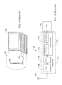
- FIG. 1A is a schematic diagram showing a conventional digital TV receiver applied to a host.
- a digital TV receiver 120 when a user watches a digital TV by using a host 100, he or she needs to connect a digital TV receiver 120 via a connector (such as a universal serial bus connecter (USB) of the host 100, and application programs of the digital TV is installed in the host 100.
- the digital TV receiver 120 includes an antenna 125 and a control unit 128.
- the antenna 125 is used for receiving a broadcasting signal of the digital TV, and the control unit 128 further converts the broadcasting signal to a selected channel signal.
- the selected channel signal is the channel selected by the user and transmitted to the host 100.
- FIG. 1B is a block diagram showing a conventional digital TV receiver.
- the control unit 128 of the digital TV receiver 120 includes a low noise amplifier (LNA) 150, a band-pass filter (BPF) 160 and a digital video broadcast (DVB) module 170.
- the DVB module 170 further includes a radio frequency (RF) tuner 172 and a demodulator 174.
- LNA low noise amplifier
- BPF band-pass filter
- RF radio frequency
- the BPF 160 keeps the digital TV bandwidth (about 450MHz to 870MHz) of the RF signal and transmits it to the DVB module 170.
- the DVB module 170 retrieves the selected channel according to the user's instruction and outputs the selected channel signal to the host 100, and the host 100 shows the content of the channel on the screen.
- the RF tuner 172 processes the bandwidth of the selected channel to a base band signal according to the user's instruction, and the demodulator 174 demodulates the base band signal and converts it to the selected channel signal.
- the digital TV system includes the DVB-T system in Europe, the advanced television system committee (ATSC) system in America, the integrated service digital broadcasting (ISDB-T) system in Japan and south America, the digital media broadcasting (DMB-T/H) system in China and so on.
- the digital TV bandwidth of the systems above is approximately between 460MHz to 870MHz.
- the bandwidth of the DVB-S satellite digital TV system is approximately between 950MHz to 2150MHz, and the bandwidth of the ISDB-S satellite digital TV system is approximately between 11.7GHz to 12.2GHz.
- the length of the antenna is in inverse proportion to a receiving frequency, since the size of the antenna applied to the digital TV in market is large, the antenna cannot be disposed inside the host 100 which is relatively small.
- the electromagnetic interference occurs in the host 100 in a conventional use, therefore, if the conventional antenna of the digital TV is disposed inside the host 100, the bad receiving signal due to EMI impact would lead to malfunction of the digital TV and cannot be watched.
- a differential antenna of a digital TV and a control system thereof is provided. Different matching circuits are used to optimize different signals of the bandwidth, and thus the size of an antenna can be reduced greatly.
- the antenna may be disposed inside any electrical device of the digital TV, and a differential RF signal generated by the antenna resists the EMI of the electrical device effectively.
- a control system of a digital TV is provided to receive a digital TV bandwidth which includes a differential antenna receiving a broadcasting signal and generating a differential RF signal including a positive signal and a negative signal; a control unit generating a selecting signal according to a selected channel; and a switch circuit including a plurality of matching circuits and a switch control circuit.
- the switch control circuit receives the selecting signal to control that an optimized positive signal is generated to the control unit after the positive signal passes through a first matching circuit of the matching circuits and an optimized negative signal is generated to the control unit after the negative signal passes through a second matching circuit of the matching circuits, the first matching circuit and the second matching circuit optimize the same bandwidth, the optimized positive signal and the optimized negative signal are a differential optimized signal, and the control unit receives the differential optimized signal and converts the differential optimized signal to a selected channel signal.
- An antenna circuit of a digital TV is further provided for receiving a digital TV bandwidth which includes a differential antenna receiving a broadcasting signal and generating a differential RF signal.
- the differential RF signal includes a positive signal and a negative signal
- a switch circuit includes a plurality of matching circuits and a switch control circuit.
- Each of the matching circuits optimizes part of the digital TV bandwidth
- the switch control circuit receives the selecting signal to control that an optimized positive signal is generated to the control unit after the positive signal passes through a first matching circuit of the matching circuits and an optimized negative signal is generated to the control unit after the negative signal passes through a second matching circuit of the matching circuits.
- the first matching circuit and the second matching circuit optimize the same bandwidth.
- a control system of a digital TV is further provided for receiving a digital TV bandwidth which includes a differential antenna receiving a broadcasting signal and generating a differential RF signal; a front-end circuit receiving the differential RF signal and converting it to an amplified positive signal and an amplified negative signal; a control unit generating a selecting signal according to a selected channel; and a switch circuit including a plurality of matching circuits and a switch control circuit.
- the switch control circuit receives the selecting signal to control that an optimized positive signal is generated to the control unit after the positive signal passes through a first matching circuit of the matching circuits and an optimized negative signal is generated to the control unit after the negative signal passes through a second matching circuit of the matching circuits, the first matching circuit and the second matching circuit optimize the same bandwidth, the optimized positive signal and the optimized negative signal are a differential optimized signal, and the control unit receives the differential optimized signal and converts it to a selected channel signal.
- An antenna circuit applied to a digital TV is further provided for receiving a digital TV bandwidth which includes a differential antenna receiving a broadcasting signal and generating a differential RF signal; a front-end circuit receiving the differential RF signal and converting it to an amplified positive signal and an amplified negative signal; a switch circuit including a plurality of matching circuits and a switch control circuit.
- the switch control circuit receives a selecting signal to control that an optimized positive signal is generated to the control unit after the positive signal passes through a first matching circuit of the matching circuits and an optimized negative signal is generated to the control unit after the negative signal passes through a second matching circuit of the matching circuits, the optimized positive signal and the optimized negative signal are a differential optimized signal, and the first matching circuit and the second matching circuit optimize the same bandwidth.
- a control system of a digital TV is further provided for receiving a digital TV bandwidth which includes a differential antenna receiving a broadcasting signal and generating a differential RF signal; a front-end circuit receiving the differential RF signal and generating a single ended signal; a DVB module generating a selecting signal according to a selected channel; and a switch circuit including a plurality of matching circuits and a switch control circuit.
- Each of the matching circuits optimizes part of the digital TV bandwidth, and the switch control circuit receives the selecting signal to control that a single ended optimized signal is generated to the DVB module after the single ended signal passes through a first matching circuit of the matching circuits.
- the DVB module converts the single ended optimized signal to a selected channel signal.
- An antenna circuit of the digital TV is further provided for receiving a digital TV bandwidth which includes a differential antenna receiving a broadcasting signal and generating a differential RF signal; a front-end circuit receiving the differential RF signal and converting a single ended signal; and a switch circuit including a plurality of the matching circuits and a switch control circuit.
- Each of the matching circuits optimizes part of the digital TV bandwidth, and the switch control circuit receives a selecting signal to control that a single ended optimized signal is generated after the single ended signal passes through a first matching circuit of the matching circuits.
- FIG. 1A is a schematic diagram showing a conventional digital TV receiving system applied to a host
- FIG. 1B is a block diagram showing a conventional digital TV receiver
- FIG. 2 is a schematic diagram showing a digital TV receiving system in an embodiment of the invention
- FIG. 3 is a block diagram showing a digital TV receiver in a first embodiment of the invention
- FIG. 4A to FIG. 4D are schematic diagrams showing matching circuits in different embodiments.
- FIG. 5 is a block diagram showing a digital TV receiver in a second embodiment of the invention.
- FIG. 6 is a block diagram showing a digital TV receiver in a third embodiment of the invention.
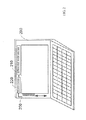
- FIG. 2 is a schematic diagram showing a digital TV receiving system in an embodiment of the invention.
- the digital TV receiving system is disposed at an available area at the edge of the screen of a host 200, which is not limited herein.
- the digital TV receiving system may be also disposed in any electrical device such as a digital TV set-top box (STB), a satellite digital TV receiver, a car audio and a video receiver, or a TV which can receive the digital TV signal.
- STB digital TV set-top box
- satellite digital TV receiver a satellite digital TV receiver
- car audio and a video receiver or a TV which can receive the digital TV signal.
- the digital TV receiving system includes a differential antenna 210, a switch circuit 220, and a control unit 250.
- the differential antenna 210 is used for receiving a broadcasting signal and generating a differential RF signal
- the switch circuit 220 is connected between the differential antenna 210 and the control unit 250.
- the switch circuit 220 optimizes a specific bandwidth corresponding to a selected channel of the differential RF signal. Afterwards, a differential optimized signal is outputted.
- the control unit 250 converts the differential optimized signal to a selected channel signal selected by the user and transmits the selected channel signal to an internal circuit of the host 200. Thus, the host 200 displays the content of the selected channel on the screen.
- the common mode noise of the EMI in the host 200 or other electrical devices is strong.
- the differential antenna 210 is used to restrain the common mode noise effectively according to an embodiment of the invention.
- the switch circuit 220 is used to optimize the bandwidth corresponding to the channel selected by the user and output the differential optimized signal to the control unit 250. Consequently, the size of the differential antenna 210 can be reduced to be smaller than 10cm, and it is easy to dispose the differential antenna 210 at the available area at the edge of the screen.
- FIG. 3 is a block diagram showing a digital TV receiver in a first embodiment of the invention.
- the differential antenna 210 uses a dipole antenna. Except for the dipole antenna, a loop antenna may also be used as the differential antenna 210.
- the differential RF signal outputted by the differential antenna 210 includes a positive signal S+ and a negative signal S-.
- the switch circuit 220 includes a switch control circuit including multiple switches Sw1 to Sw4 and a plurality of matching circuits 221 to 228, and the control unit 250 may output a 2-bit selecting signal to the switches Sw1 to Sw4 of the switch circuit 220.
- the matching circuits 221 to 228 optimize the different bandwidths of the digital TV bandwidth, and improve the receiving efficiency of the bandwidth.
- the first switch Sw1 inputs the positive signal S+ to the 450-550MHz matching circuit 221 which optimizes the signal with the 450 MHz to 550MHz bandwidth in the positive signal S+, and the optimized positive signal So+ is outputted by the second switch Sw2; when the selecting signal is "01", the first switch Sw1 inputs the positive signal S+ to the 550-650MHz matching circuit 223 which optimizes the signal with the 550MHz to 650MHz bandwidth in the positive signal S+, and the optimized positive signal So+ is outputted by the second switch Sw2; when the selecting signal is "10", the first switch Sw1 inputs the positive signal S+ to the 650-750MHz matching circuit 225 which optimizes the signal with the 650MHz to 754MHz bandwidth in the positive signal S+, and the optimized positive signal So+ is outputted by the second switch Sw2; when the selecting signal is "11", the first switch Sw1 inputs the positive signal S+ to the 750-870MHz matching circuit 227 which optimizes the signal with the 750MHz
- the principle of the actions to the negative signal S- by the third switch Sw3, the fourth switch Sw4, and the matching circuits 222, 224, 226, 228 are the same as the above principle, which is omitted herein.
- the optimized positive signal So+ and the optimized negative signal so- are the differential optimized signal.
- the control unit 250 includes a prepositive circuit 251 and a DVB module 256.
- the prepositive circuit 251 includes a differential LNA 252 and a balun 254.
- the DVB module 256 further includes a RF tuner 257 and a demodulator 258.
- the differential LNA 252 of the prepositive circuit 251 receives and amplifies the differential optimized signal.
- the balun 254 converts the differential optimized signal to a single ended optimized signal and inputs the single ended optimized signal to the DVB module 256.
- the DVB module 256 outputs the selecting signal according to the user's instruction, retrieves the selected channel from the single ended optimized signal and converts it to the selected channel signal to output to the host (or the electrical device).
- the host (or the electrical device) displays video on the corresponding screen.
- the RF tuner 257 converts the single ended optimized signal to the base band signal according to the user's instruction.
- the demodulator 258 outputs the selecting signal according to the user's instruction, demodulates the base band signal and converts it to the selected channel signal.
- the selected channel is transmitted to the DVB module 256.
- the demodulator 258 of the DVB module 256 outputs the selecting signal to the switch circuit 220, and the DVB module 256 converts the received single ended optimized signal to the selected channel signal. For example, if the selected channel is between 650MHz and 750 MHz, the demodulator 258 outputs the selecting signal "10" to the switches Sw1 to Sw4.
- the optimized positive signal So+ is generated after the positive signal S+ passes through the 650-750MHz matching circuit 225, and the optimized negative signal so- is also generated after the negative signal S- passes through the 650-750MHz matching circuit 226.
- the single ended optimized signal is inputted into the DVB module 256 after it passes through the differential LNA 252 and the balun 254.
- the DVB module 256 outputs the selected channel signal to the host (or the electrical device), and the video is displayed on the corresponding screen.
- the matching circuits may be a T-shaped circuit or a ⁇ -shaped circuit.
- the T-shaped circuit includes two inductors Lt1 and Lt2 connected in series between the input end S and the output end So.
- a capacitor Ct is connected between a connector point of the two inductors Lt1, Lt2 and a ground.
- the T-shaped circuit includes two capacitors Ct1 and Ct2 connected in series between the input end S and the output end So.
- An inductor Lt is connected between the connector point of the two capacitors Ct1, Ct2 and the ground.
- the ⁇ -shaped circuit includes an inductor Lp connected between the input end S and the output end So, a capacitor Cp1 connected between the input end S and the ground, and a capacitor Cp2 connected between the output end So and the ground.
- the ⁇ -shaped circuit includes a capacitor Cp connected between the input end S and the output end so, an inductor Lp 1 connected between the input end S and the ground, and an inductor Lp2 connected between the output end so and the ground.
- the matching circuits with different bandwidths can be obtained by adjusting the value of the inductor and the capacitor of the T-shaped circuit or the ⁇ -shape circuit.
- the switch circuit is used to optimize the signal with different bandwidths to reduce the size of the differential antenna.
- a common mode filter may be added between the input end of the switch circuit 220 and the output end of the differential LNA 252 to filter the common mode noise completely.
- FIG. 5 is a block diagram showing a digital TV receiver in a second embodiment of the invention.
- the digital TV receiver includes a differential antenna 310, a front-end circuit 320, a switch circuit 330, and a control unit 350.
- the front-end circuit 320 is a differential LNA 322.
- the differential antenna 310 receives the broadcasting signal and outputs the differential RF signal which includes a positive signal S+ and a negative signal S-.
- the differential LNA 322 receives the differential RF signal and converts it to an amplified differential RF signal which includes an amplified positive signal Si+ and an amplified negative signal Si-.
- the switch circuit 330 includes the switch control circuit including multiple switches Sw1 to Sw4 and a plurality of the matching circuits 331 to 338.
- the control unit 350 outputs a 2-bit selecting signal to the switches Sw1 to Sw4 of the switch circuit 330.
- the matching circuits 331 to 338 optimize the different bandwidths of the digital TV the bandwidth, and improve the receiving efficiency of the bandwidth.
- the first switch Sw1 inputs the amplified positive signal Si+ to the 450-550MHz matching circuit 331 which optimizes the signal with the 450MHz to 550MHz bandwidth in the amplified positive signal Si+, and then the optimized positive signal So+ is generated and outputted by the second switches Sw2;
- the selecting signal is "01”
- the first switch Sw1 inputs the amplified positive signal Si+ to the 550-650MHz matching circuit 333 which optimizes the signal with the 550MHz to 650MHz bandwidth in the amplified positive signal Si+, and then the optimized positive signal So+ is generated and outputted by the second switches Sw2;
- the selecting signal is "10”
- the first switch Sw1 inputs the amplified positive signal Si+ to the 650-750MHz matching circuit 335 which optimizes the signal with the 650MHz to 750MHz bandwidth in the amplified positive signal Si+, and then the optimized positive signal So+ is generated and outputted by the second switches Sw2;
- the selecting signal is "11"
- the first switch Sw1 inputs the
- the principle of actions to the amplified negative signal Si- by the third switch Sw3, the fourth switch Sw4, and the matching circuits 332, 334, 336, 338 are the same as the above principle, which is omitted herein.
- the optimized positive signal So+ and the optimized negative signal so- are the differential optimized signal.
- the control unit 350 includes a prepositive circuit 351 and a DVB module 356.
- the prepositive circuit 351 is a balun
- the DVB module 356 includes a RF tuner 357 and a demodulator 358.
- the balun 352 converts the differential optimized signal to the single ended optimized signal and inputs it to the DVB module 356.
- the DVB module 356 outputs the selecting signal according to the user's instruction, retrieves the selected channel from the single ended optimized signal and converts it to the selected channel signal to the host (or the electrical device).
- the host (or the electrical device) displays video signal on the corresponding screen.
- the RF tuner 357 converts the single ended optimized signal to the base band signal according to the user's instruction.
- the demodulator 358 outputs the selecting signal according to the user's instruction, demodulates the base band signal and converts it to the selected channel signal.
- the selected channel is transmitted to the DVB module 356.
- the demodulator 358 of the DVB module 356 outputs the selecting signal to the switch circuit 330, and the DVB module 356 converts the received single ended optimized signal to the selected channel signal. For example, if the selected channel is in 650MHz to 750MHz, the demodulator 358 outputs the "10" selecting signal to the switches Sw1 to Sw4.
- the optimized positive signal So+ is generated Similarly, after the amplified negative signal Si- passes through the 650-750MHz matching circuit 336, the optimized negative signal So- is generated after the control unit 350 receives the differential optimized signal, the single ended optimized signal is inputted to the DVB module 356 after it passes through the balun 352. Then, the DVB module 356 outputs the selected channel signal to the host (or the electrical device), and the video is displayed on the corresponding screen.
- Persons having ordinary skill in the art may further add a common mode filter to the front-end circuit 320 or the prepositive circuit 351 of the digital TV receiver in the second embodiment to filter the common mode noise completely.
- FIG. 6 is a block diagram showing a digital TV receiver in a third embodiment of the invention.
- the digital TV receiver includes a differential antenna 410, a front-end circuit 420, a switch circuit 430, and a DVB module 450.
- the differential antenna 410 receives the broadcasting signal and converts it to the differential RF signal which includes a positive signal S+ and a negative signal S-.
- the front-end circuit 420 receives the differential RF signal and converts it to a single ended signal.
- the front-end circuit 420 further includes a differential LNA 422 and a balun 424.
- the differential LNA 422 receives and amplifies the differential RF signal.
- the balun 424 converts the amplified differential RF signal to the single ended signal S.
- the switch circuit 430 includes the switch control circuit including multiple switches Sw1 to Sw2 and a plurality of the matching circuits 432 to 435, and the DVB module 450 may output the 2-bit selecting signal to the switches Sw1 to Sw2 of the switch circuit 430.
- the matching circuits 432 to 435 optimize the digital TV bandwidth with different bandwidths, and improve the receiving efficiency of the bandwidth.
- the first switches Sw1 inputs the single ended signal S to the 450-550MHz matching circuit 432 which optimizes the signal with the 450MHz to 550MHz bandwidth in the single ended signal S, and the single ended optimized signal So is outputted by the second switches Sw2; when the selecting signal is "01", the first switches Sw1 inputs the single ended signal S to the 550-650MHz matching circuit 433 which optimizes the signal with the 550MHz to 650MHz bandwidth in the single ended signal S, and the single ended optimized signal So is outputted by the second switches Sw2; when the selecting signal is "10", the first switches Sw1 inputs the single ended signal S to the 650-750MHz matching circuit 434 which optimizes the signal with the 650MHz to 750MHz bandwidth in the single ended signal S, and the single ended optimized signal So is outputted by the second switches Sw2; when the selecting signal is "1", the first switches Sw1 inputs the single ended signal S to the 750-870MHz matching circuit 435 which optimizes the signal with the 750MHz to
- the DVB module 450 outputs the selecting signal according to the user's instruction, retrieves the selected channel selected by the user from the single ended optimized signal and converts it to the selected channel signal to the host (or the electrical device).
- the host (or the electrical device) displays the content of the channel signal on the corresponding screen.
- the DVB module 450 further includes a RF tuner 457 and a demodulator 458.
- the RF tuner 457 converts the single ended optimized signal to the base band signal according to the user's instruction.
- the demodulator 458 outputs the selecting signal according to the user's instruction, demodulates the base band signal and converts it to the selected channel signal.
- the selected channel is transmitted to the DVB module 450.
- the demodulator 458 of the DVB module 450 outputs the selecting signal to the switch circuit 430, and the DVB module 450 converts the received single ended optimized signal to the selected channel signal. For example, if the selected channel is between 650 MHz to 750MHz, the demodulator 458 outputs the "10" selecting signal to the switches Sw1 to Sw2.
- the single ended optimized signal So is generated after the single ended signal S passes through the 650-750MHz matching circuit 434.
- the DVB module 450 receives the single ended optimized signal So, and then it can output the selected channel signal to the host (or the electrical device), and the content of the selected channel is displayed on the corresponding screen.
- the number of the matching circuits is not limited herein. Persons having ordinary skill in the art may design the matching circuits with different bandwidths, and match with the switch control circuit including different switches to achieve the switch circuit in the embodiment.
- the antenna and the digital TV receiver take the digital TV bandwidth 450MHz to 870MHz as an example, they may also be applied to a DVB-S satellite digital TV system or an ISDB-S satellite digital TV system.
- front-end circuit may change the front-end circuit, for example, they may exchange the positions of the differential LNA 422 and the balun 424 of the front-end circuit 420 in the third embodiment, or convert the differential RF signal to the single ended signal.
- the digital TV receiving system is not limited to be disposed in the host (or the electrical device). Persons having ordinary skill in the art also may dispose the receiving system outside the host (or the electrical device) to achieve the same effect.
Landscapes
- Engineering & Computer Science (AREA)
- Signal Processing (AREA)
- Multimedia (AREA)
- Computer Hardware Design (AREA)
- General Engineering & Computer Science (AREA)
- Theoretical Computer Science (AREA)
- Human Computer Interaction (AREA)
- Physics & Mathematics (AREA)
- General Physics & Mathematics (AREA)
- Computer Networks & Wireless Communication (AREA)
- Input Circuits Of Receivers And Coupling Of Receivers And Audio Equipment (AREA)
- Details Of Aerials (AREA)
- Support Of Aerials (AREA)
Abstract
A differential antenna and associated control system applied to a digital television (TV). The control system includes a differential antenna receiving a broadcasting signal and generating a differential radio frequency (RF) signal including a positive signal and a negative signal; a control unit generating a selecting signal according to a selected channel; a switch circuit including a switch control circuit and a plurality of matching circuits. Each of the matching circuits optimizes part of the digital TV bandwidth, and the switch control circuit receives the selecting signal to control that an optimized positive signal is generated to the control unit after the positive signal passes through a first matching circuit of the matching circuits, and an optimized negative signal is generated to the control unit after the negative signal passes through a second matching circuit of the matching circuits. The first matching circuit and the second matching circuit optimize the same frequency band, and a differential optimizing signal includes the optimized positive signal and the optimized negative signal. Thus, the control unit generates a selected channel signal accordingly.
Description
- The invention relates to an antenna and a control system thereof and, more particularly, to a differential antenna and a control system applied to a digital television (TV).
-
FIG. 1A is a schematic diagram showing a conventional digital TV receiver applied to a host. Generally, when a user watches a digital TV by using ahost 100, he or she needs to connect adigital TV receiver 120 via a connector (such as a universal serial bus connecter (USB) of thehost 100, and application programs of the digital TV is installed in thehost 100. Thedigital TV receiver 120 includes anantenna 125 and acontrol unit 128. Theantenna 125 is used for receiving a broadcasting signal of the digital TV, and thecontrol unit 128 further converts the broadcasting signal to a selected channel signal. The selected channel signal is the channel selected by the user and transmitted to thehost 100. -
FIG. 1B is a block diagram showing a conventional digital TV receiver. Thecontrol unit 128 of thedigital TV receiver 120 includes a low noise amplifier (LNA) 150, a band-pass filter (BPF) 160 and a digital video broadcast (DVB)module 170. The DVBmodule 170 further includes a radio frequency (RF)tuner 172 and ademodulator 174. - First, after the LNA 150 amplifies the RF signal, the
BPF 160 keeps the digital TV bandwidth (about 450MHz to 870MHz) of the RF signal and transmits it to theDVB module 170. Second, the DVBmodule 170 retrieves the selected channel according to the user's instruction and outputs the selected channel signal to thehost 100, and thehost 100 shows the content of the channel on the screen. TheRF tuner 172 processes the bandwidth of the selected channel to a base band signal according to the user's instruction, and thedemodulator 174 demodulates the base band signal and converts it to the selected channel signal. - It is well-known that the digital TV system includes the DVB-T system in Europe, the advanced television system committee (ATSC) system in America, the integrated service digital broadcasting (ISDB-T) system in Japan and south America, the digital media broadcasting (DMB-T/H) system in China and so on. The digital TV bandwidth of the systems above is approximately between 460MHz to 870MHz. The bandwidth of the DVB-S satellite digital TV system is approximately between 950MHz to 2150MHz, and the bandwidth of the ISDB-S satellite digital TV system is approximately between 11.7GHz to 12.2GHz.
- The length of the antenna is in inverse proportion to a receiving frequency, since the size of the antenna applied to the digital TV in market is large, the antenna cannot be disposed inside the
host 100 which is relatively small. - Further, the electromagnetic interference (EMI) occurs in the
host 100 in a conventional use, therefore, if the conventional antenna of the digital TV is disposed inside thehost 100, the bad receiving signal due to EMI impact would lead to malfunction of the digital TV and cannot be watched. - A differential antenna of a digital TV and a control system thereof is provided. Different matching circuits are used to optimize different signals of the bandwidth, and thus the size of an antenna can be reduced greatly. The antenna may be disposed inside any electrical device of the digital TV, and a differential RF signal generated by the antenna resists the EMI of the electrical device effectively.
- A control system of a digital TV is provided to receive a digital TV bandwidth which includes a differential antenna receiving a broadcasting signal and generating a differential RF signal including a positive signal and a negative signal; a control unit generating a selecting signal according to a selected channel; and a switch circuit including a plurality of matching circuits and a switch control circuit. Each of the matching circuits optimizes part of the digital TV bandwidth, the switch control circuit receives the selecting signal to control that an optimized positive signal is generated to the control unit after the positive signal passes through a first matching circuit of the matching circuits and an optimized negative signal is generated to the control unit after the negative signal passes through a second matching circuit of the matching circuits, the first matching circuit and the second matching circuit optimize the same bandwidth, the optimized positive signal and the optimized negative signal are a differential optimized signal, and the control unit receives the differential optimized signal and converts the differential optimized signal to a selected channel signal.
- An antenna circuit of a digital TV is further provided for receiving a digital TV bandwidth which includes a differential antenna receiving a broadcasting signal and generating a differential RF signal. The differential RF signal includes a positive signal and a negative signal, and a switch circuit includes a plurality of matching circuits and a switch control circuit. Each of the matching circuits optimizes part of the digital TV bandwidth, the switch control circuit receives the selecting signal to control that an optimized positive signal is generated to the control unit after the positive signal passes through a first matching circuit of the matching circuits and an optimized negative signal is generated to the control unit after the negative signal passes through a second matching circuit of the matching circuits. The first matching circuit and the second matching circuit optimize the same bandwidth.
- A control system of a digital TV is further provided for receiving a digital TV bandwidth which includes a differential antenna receiving a broadcasting signal and generating a differential RF signal; a front-end circuit receiving the differential RF signal and converting it to an amplified positive signal and an amplified negative signal; a control unit generating a selecting signal according to a selected channel; and a switch circuit including a plurality of matching circuits and a switch control circuit. Each of the matching circuits optimizes part of the digital TV bandwidth, the switch control circuit receives the selecting signal to control that an optimized positive signal is generated to the control unit after the positive signal passes through a first matching circuit of the matching circuits and an optimized negative signal is generated to the control unit after the negative signal passes through a second matching circuit of the matching circuits, the first matching circuit and the second matching circuit optimize the same bandwidth, the optimized positive signal and the optimized negative signal are a differential optimized signal, and the control unit receives the differential optimized signal and converts it to a selected channel signal.
- An antenna circuit applied to a digital TV is further provided for receiving a digital TV bandwidth which includes a differential antenna receiving a broadcasting signal and generating a differential RF signal; a front-end circuit receiving the differential RF signal and converting it to an amplified positive signal and an amplified negative signal; a switch circuit including a plurality of matching circuits and a switch control circuit. Each of the matching circuits optimizes part of the digital TV bandwidth, the switch control circuit receives a selecting signal to control that an optimized positive signal is generated to the control unit after the positive signal passes through a first matching circuit of the matching circuits and an optimized negative signal is generated to the control unit after the negative signal passes through a second matching circuit of the matching circuits, the optimized positive signal and the optimized negative signal are a differential optimized signal, and the first matching circuit and the second matching circuit optimize the same bandwidth.
- A control system of a digital TV is further provided for receiving a digital TV bandwidth which includes a differential antenna receiving a broadcasting signal and generating a differential RF signal; a front-end circuit receiving the differential RF signal and generating a single ended signal; a DVB module generating a selecting signal according to a selected channel; and a switch circuit including a plurality of matching circuits and a switch control circuit. Each of the matching circuits optimizes part of the digital TV bandwidth, and the switch control circuit receives the selecting signal to control that a single ended optimized signal is generated to the DVB module after the single ended signal passes through a first matching circuit of the matching circuits. The DVB module converts the single ended optimized signal to a selected channel signal.
- An antenna circuit of the digital TV is further provided for receiving a digital TV bandwidth which includes a differential antenna receiving a broadcasting signal and generating a differential RF signal; a front-end circuit receiving the differential RF signal and converting a single ended signal; and a switch circuit including a plurality of the matching circuits and a switch control circuit. Each of the matching circuits optimizes part of the digital TV bandwidth, and the switch control circuit receives a selecting signal to control that a single ended optimized signal is generated after the single ended signal passes through a first matching circuit of the matching circuits.
- These and other features, aspects and advantages of the present invention will become better understood with regard to the following description, appended claims, and accompanying drawings.
-
FIG. 1A is a schematic diagram showing a conventional digital TV receiving system applied to a host; -
FIG. 1B is a block diagram showing a conventional digital TV receiver; -
FIG. 2 is a schematic diagram showing a digital TV receiving system in an embodiment of the invention; -
FIG. 3 is a block diagram showing a digital TV receiver in a first embodiment of the invention; -
FIG. 4A to FIG. 4D are schematic diagrams showing matching circuits in different embodiments; -
FIG. 5 is a block diagram showing a digital TV receiver in a second embodiment of the invention; and -
FIG. 6 is a block diagram showing a digital TV receiver in a third embodiment of the invention. -
FIG. 2 is a schematic diagram showing a digital TV receiving system in an embodiment of the invention. The digital TV receiving system is disposed at an available area at the edge of the screen of ahost 200, which is not limited herein. The digital TV receiving system may be also disposed in any electrical device such as a digital TV set-top box (STB), a satellite digital TV receiver, a car audio and a video receiver, or a TV which can receive the digital TV signal. - In
FIG. 2 , the digital TV receiving system includes adifferential antenna 210, aswitch circuit 220, and acontrol unit 250. Thedifferential antenna 210 is used for receiving a broadcasting signal and generating a differential RF signal, and theswitch circuit 220 is connected between thedifferential antenna 210 and thecontrol unit 250. Theswitch circuit 220 optimizes a specific bandwidth corresponding to a selected channel of the differential RF signal. Afterwards, a differential optimized signal is outputted. Thecontrol unit 250 converts the differential optimized signal to a selected channel signal selected by the user and transmits the selected channel signal to an internal circuit of thehost 200. Thus, thehost 200 displays the content of the selected channel on the screen. - Generally speaking, the common mode noise of the EMI in the
host 200 or other electrical devices is strong. Thedifferential antenna 210 is used to restrain the common mode noise effectively according to an embodiment of the invention. Furthermore, to reduce the size of thedifferential antenna 210, theswitch circuit 220 is used to optimize the bandwidth corresponding to the channel selected by the user and output the differential optimized signal to thecontrol unit 250. Consequently, the size of thedifferential antenna 210 can be reduced to be smaller than 10cm, and it is easy to dispose thedifferential antenna 210 at the available area at the edge of the screen. -
FIG. 3 is a block diagram showing a digital TV receiver in a first embodiment of the invention. Thedifferential antenna 210 uses a dipole antenna. Except for the dipole antenna, a loop antenna may also be used as thedifferential antenna 210. The differential RF signal outputted by thedifferential antenna 210 includes a positive signal S+ and a negative signal S-. - The
switch circuit 220 includes a switch control circuit including multiple switches Sw1 to Sw4 and a plurality of matchingcircuits 221 to 228, and thecontrol unit 250 may output a 2-bit selecting signal to the switches Sw1 to Sw4 of theswitch circuit 220. The matchingcircuits 221 to 228 optimize the different bandwidths of the digital TV bandwidth, and improve the receiving efficiency of the bandwidth. - For example, when the selecting signal is "00", the first switch Sw1 inputs the positive signal S+ to the 450-
550MHz matching circuit 221 which optimizes the signal with the 450 MHz to 550MHz bandwidth in the positive signal S+, and the optimized positive signal So+ is outputted by the second switch Sw2; when the selecting signal is "01", the first switch Sw1 inputs the positive signal S+ to the 550-650MHz matching circuit 223 which optimizes the signal with the 550MHz to 650MHz bandwidth in the positive signal S+, and the optimized positive signal So+ is outputted by the second switch Sw2; when the selecting signal is "10", the first switch Sw1 inputs the positive signal S+ to the 650-750MHz matching circuit 225 which optimizes the signal with the 650MHz to 754MHz bandwidth in the positive signal S+, and the optimized positive signal So+ is outputted by the second switch Sw2; when the selecting signal is "11", the first switch Sw1 inputs the positive signal S+ to the 750-870MHz matching circuit 227 which optimizes the signal with the 750MHz to 870MHz bandwidth in the positive signal S+, and the optimized positive signal So+ is outputted by the second switch Sw2. The principle of the actions to the negative signal S- by the third switch Sw3, the fourth switch Sw4, and the matchingcircuits - The
control unit 250 includes aprepositive circuit 251 and aDVB module 256. Theprepositive circuit 251 includes adifferential LNA 252 and abalun 254. TheDVB module 256 further includes aRF tuner 257 and ademodulator 258. - The
differential LNA 252 of theprepositive circuit 251 receives and amplifies the differential optimized signal. Afterwards, thebalun 254 converts the differential optimized signal to a single ended optimized signal and inputs the single ended optimized signal to theDVB module 256. TheDVB module 256 outputs the selecting signal according to the user's instruction, retrieves the selected channel from the single ended optimized signal and converts it to the selected channel signal to output to the host (or the electrical device). The host (or the electrical device) displays video on the corresponding screen. Furthermore, theRF tuner 257 converts the single ended optimized signal to the base band signal according to the user's instruction. Thedemodulator 258 outputs the selecting signal according to the user's instruction, demodulates the base band signal and converts it to the selected channel signal. - After the user selects a channel in the host (or the electrical device), the selected channel is transmitted to the
DVB module 256. Thedemodulator 258 of theDVB module 256 outputs the selecting signal to theswitch circuit 220, and theDVB module 256 converts the received single ended optimized signal to the selected channel signal. For example, if the selected channel is between 650MHz and 750 MHz, thedemodulator 258 outputs the selecting signal "10" to the switches Sw1 to Sw4. Similarly, the optimized positive signal So+ is generated after the positive signal S+ passes through the 650-750MHz matching circuit 225, and the optimized negative signal so- is also generated after the negative signal S- passes through the 650-750MHz matching circuit 226. After thecontrol unit 250 receives the differential optimized signal, the single ended optimized signal is inputted into theDVB module 256 after it passes through thedifferential LNA 252 and thebalun 254. TheDVB module 256 outputs the selected channel signal to the host (or the electrical device), and the video is displayed on the corresponding screen. - As shown in
FIG. 4A to FIG. 4D , the matching circuits may be a T-shaped circuit or a π-shaped circuit. InFIG. 4A , the T-shaped circuit includes two inductors Lt1 and Lt2 connected in series between the input end S and the output end So. A capacitor Ct is connected between a connector point of the two inductors Lt1, Lt2 and a ground. InFIG. 4B , the T-shaped circuit includes two capacitors Ct1 and Ct2 connected in series between the input end S and the output end So. An inductor Lt is connected between the connector point of the two capacitors Ct1, Ct2 and the ground. InFIG. 4C , the π-shaped circuit includes an inductor Lp connected between the input end S and the output end So, a capacitor Cp1 connected between the input end S and the ground, and a capacitor Cp2 connected between the output end So and the ground. InFIG. 4D , the π-shaped circuit includes a capacitor Cp connected between the input end S and the output end so, aninductor Lp 1 connected between the input end S and the ground, and an inductor Lp2 connected between the output end so and the ground. The matching circuits with different bandwidths can be obtained by adjusting the value of the inductor and the capacitor of the T-shaped circuit or the π-shape circuit. - As stated above, the switch circuit is used to optimize the signal with different bandwidths to reduce the size of the differential antenna. Persons having ordinary skill in the art may make various modifications and changes according to the switch circuit in the embodiment. For example, in
FIG. 3 , a common mode filter may be added between the input end of theswitch circuit 220 and the output end of thedifferential LNA 252 to filter the common mode noise completely. -
FIG. 5 is a block diagram showing a digital TV receiver in a second embodiment of the invention. The digital TV receiver includes adifferential antenna 310, a front-end circuit 320, aswitch circuit 330, and acontrol unit 350. The front-end circuit 320 is adifferential LNA 322. - According to the second embodiment of the invention, the
differential antenna 310 receives the broadcasting signal and outputs the differential RF signal which includes a positive signal S+ and a negative signal S-. Thedifferential LNA 322 receives the differential RF signal and converts it to an amplified differential RF signal which includes an amplified positive signal Si+ and an amplified negative signal Si-. - The
switch circuit 330 includes the switch control circuit including multiple switches Sw1 to Sw4 and a plurality of the matchingcircuits 331 to 338. Thecontrol unit 350 outputs a 2-bit selecting signal to the switches Sw1 to Sw4 of theswitch circuit 330. The matchingcircuits 331 to 338 optimize the different bandwidths of the digital TV the bandwidth, and improve the receiving efficiency of the bandwidth. - For example, when the selecting signal is "00", the first switch Sw1 inputs the amplified positive signal Si+ to the 450-
550MHz matching circuit 331 which optimizes the signal with the 450MHz to 550MHz bandwidth in the amplified positive signal Si+, and then the optimized positive signal So+ is generated and outputted by the second switches Sw2; when the selecting signal is "01", the first switch Sw1 inputs the amplified positive signal Si+ to the 550-650MHz matching circuit 333 which optimizes the signal with the 550MHz to 650MHz bandwidth in the amplified positive signal Si+, and then the optimized positive signal So+ is generated and outputted by the second switches Sw2; when the selecting signal is "10", the first switch Sw1 inputs the amplified positive signal Si+ to the 650-750MHz matching circuit 335 which optimizes the signal with the 650MHz to 750MHz bandwidth in the amplified positive signal Si+, and then the optimized positive signal So+ is generated and outputted by the second switches Sw2; when the selecting signal is "11", the first switch Sw1 inputs the amplified positive signal Si+ to the 750-870MHz matching circuit 337 which optimizes the signal with the 750MHz to 870MHz bandwidth in the amplified positive signal Si+, and then the optimized positive signal So+ is generated and outputted by the second switches Sw2. The principle of actions to the amplified negative signal Si- by the third switch Sw3, the fourth switch Sw4, and the matchingcircuits - The
control unit 350 includes aprepositive circuit 351 and aDVB module 356. Theprepositive circuit 351 is a balun, and theDVB module 356 includes aRF tuner 357 and ademodulator 358. - The
balun 352 converts the differential optimized signal to the single ended optimized signal and inputs it to theDVB module 356. TheDVB module 356 outputs the selecting signal according to the user's instruction, retrieves the selected channel from the single ended optimized signal and converts it to the selected channel signal to the host (or the electrical device). The host (or the electrical device) displays video signal on the corresponding screen. TheRF tuner 357 converts the single ended optimized signal to the base band signal according to the user's instruction. Thedemodulator 358 outputs the selecting signal according to the user's instruction, demodulates the base band signal and converts it to the selected channel signal. - After the user determines a selected channel at the host (or the electrical device), the selected channel is transmitted to the
DVB module 356. Thedemodulator 358 of theDVB module 356 outputs the selecting signal to theswitch circuit 330, and theDVB module 356 converts the received single ended optimized signal to the selected channel signal. For example, if the selected channel is in 650MHz to 750MHz, thedemodulator 358 outputs the "10" selecting signal to the switches Sw1 to Sw4. Thus, after the amplified positive signal Si+ passes through the 650-750MHz matching circuit 335, the optimized positive signal So+ is generated Similarly, after the amplified negative signal Si- passes through the 650-750MHz matching circuit 336, the optimized negative signal So- is generated after thecontrol unit 350 receives the differential optimized signal, the single ended optimized signal is inputted to theDVB module 356 after it passes through thebalun 352. Then, theDVB module 356 outputs the selected channel signal to the host (or the electrical device), and the video is displayed on the corresponding screen. - Persons having ordinary skill in the art may further add a common mode filter to the front-
end circuit 320 or theprepositive circuit 351 of the digital TV receiver in the second embodiment to filter the common mode noise completely. -
FIG. 6 is a block diagram showing a digital TV receiver in a third embodiment of the invention. The digital TV receiver includes adifferential antenna 410, a front-end circuit 420, aswitch circuit 430, and aDVB module 450. Thedifferential antenna 410 receives the broadcasting signal and converts it to the differential RF signal which includes a positive signal S+ and a negative signal S-. - The front-
end circuit 420 receives the differential RF signal and converts it to a single ended signal. The front-end circuit 420 further includes adifferential LNA 422 and abalun 424. Thedifferential LNA 422 receives and amplifies the differential RF signal. Afterwards, thebalun 424 converts the amplified differential RF signal to the single ended signal S. - The
switch circuit 430 includes the switch control circuit including multiple switches Sw1 to Sw2 and a plurality of the matchingcircuits 432 to 435, and theDVB module 450 may output the 2-bit selecting signal to the switches Sw1 to Sw2 of theswitch circuit 430. The matchingcircuits 432 to 435 optimize the digital TV bandwidth with different bandwidths, and improve the receiving efficiency of the bandwidth. - For example, when the selecting signal is "00", the first switches Sw1 inputs the single ended signal S to the 450-
550MHz matching circuit 432 which optimizes the signal with the 450MHz to 550MHz bandwidth in the single ended signal S, and the single ended optimized signal So is outputted by the second switches Sw2; when the selecting signal is "01", the first switches Sw1 inputs the single ended signal S to the 550-650MHz matching circuit 433 which optimizes the signal with the 550MHz to 650MHz bandwidth in the single ended signal S, and the single ended optimized signal So is outputted by the second switches Sw2; when the selecting signal is "10", the first switches Sw1 inputs the single ended signal S to the 650-750MHz matching circuit 434 which optimizes the signal with the 650MHz to 750MHz bandwidth in the single ended signal S, and the single ended optimized signal So is outputted by the second switches Sw2; when the selecting signal is "1", the first switches Sw1 inputs the single ended signal S to the 750-870MHz matching circuit 435 which optimizes the signal with the 750MHz to 870MHz bandwidth in the single ended signal S, and the single ended optimized signal So is outputted by the second switches Sw2. - The
DVB module 450 outputs the selecting signal according to the user's instruction, retrieves the selected channel selected by the user from the single ended optimized signal and converts it to the selected channel signal to the host (or the electrical device). The host (or the electrical device) displays the content of the channel signal on the corresponding screen. TheDVB module 450 further includes aRF tuner 457 and ademodulator 458. TheRF tuner 457 converts the single ended optimized signal to the base band signal according to the user's instruction. Thedemodulator 458 outputs the selecting signal according to the user's instruction, demodulates the base band signal and converts it to the selected channel signal. - When the user determines a selected channel at the host (or the electrical device), the selected channel is transmitted to the
DVB module 450. Thedemodulator 458 of theDVB module 450 outputs the selecting signal to theswitch circuit 430, and theDVB module 450 converts the received single ended optimized signal to the selected channel signal. For example, if the selected channel is between 650 MHz to 750MHz, thedemodulator 458 outputs the "10" selecting signal to the switches Sw1 to Sw2. Thus, the single ended optimized signal So is generated after the single ended signal S passes through the 650-750MHz matching circuit 434. TheDVB module 450 receives the single ended optimized signal So, and then it can output the selected channel signal to the host (or the electrical device), and the content of the selected channel is displayed on the corresponding screen. - Besides, the number of the matching circuits is not limited herein. Persons having ordinary skill in the art may design the matching circuits with different bandwidths, and match with the switch control circuit including different switches to achieve the switch circuit in the embodiment. Moreover, although the antenna and the digital TV receiver take the digital TV bandwidth 450MHz to 870MHz as an example, they may also be applied to a DVB-S satellite digital TV system or an ISDB-S satellite digital TV system.
- Persons having ordinary skill in the art may change the front-end circuit, for example, they may exchange the positions of the
differential LNA 422 and thebalun 424 of the front-end circuit 420 in the third embodiment, or convert the differential RF signal to the single ended signal. - Although the antenna circuit of the digital TV and the receiving system are disposed in the host (or the electrical device), the digital TV receiving system is not limited to be disposed in the host (or the electrical device). Persons having ordinary skill in the art also may dispose the receiving system outside the host (or the electrical device) to achieve the same effect.
- Although the present invention has been described in considerable detail with reference to certain preferred embodiments thereof, the disclosure is not for limiting the scope of the invention. Persons having ordinary skill in the art may make various modifications and changes without departing from the scope. Therefore, the scope of the appended claims should not be limited to the description of the preferred embodiments described above.
Claims (17)
- A control system of a digital television (TV) receiving a digital TV bandwidth, characterized by comprising:a differential antenna (210) receiving broadcasting signal and generating a differential radio frequency (RF) signal including a positive signal and a negative signal;a control unit (250) generating a selecting signal according to a selected channel; anda switch circuit (220) including a plurality of matching circuits (221∼228) and a switch control circuit,wherein each of the matching circuits (221∼228) optimizes part of the digital TV bandwidth, the switch control circuit receives the selecting signal to control that an optimized positive signal is generated to the control unit (250) after the positive signal passes through a first matching circuit (221, 223, 225, 227) of the matching circuits (221∼228) and an optimized negative signal is generated to the control mit (250) after the negative signal passes through a second matching circuit (222, 224, 226, 228) of the matching circuits (221∼228), the first matching circuit (221, 223, 225, 227) and the second matching circuit (222, 224, 226, 228) optimize the same bandwidth, the optimized positive signal and the optimized negative signal are a differential optimized signal, and the control unit (250) receives the differential optimized signal and converts the differential optimized signal to a selected channel signal.
- The control system according to claim 1, characterized in that the control unit (250) comprises:a prepositive circuit (251) receiving the differential optimized signal and generating a single ended optimized signal; anda digital video broadcast (DVB) module (256) converting the single ended optimized signal to the selected channel signal according to the selected channel.
- The control system according to claim 2, characterized in that the prepositive circuit (251) comprises:a differential low noise amplifier (LNA) (252) receiving and amplifying the differential optimized signal; anda balun (254) converting the amplified differential optimized signal to the single ended optimized signal.
- A control system of a digital TV receiving a digital TV bandwidth, characterized by comprising:a differential antenna (410) receiving broadcasting signal and generating a differential RF signal;a front-end circuit (420) receiving the differential RF signal and generating a single ended signal;a DVB module (450) generating a selecting signal according to a selected channel; anda switch circuit (430) including a plurality of matching circuits (432∼435) and a switch control circuit, wherein each of the matching circuits (432∼435) optimizes part of the digital TV bandwidth, the switch control circuit receives the selecting signal to control that a single ended optimized signal is generated to the DVB module (450) after the single ended signal passes through a first matching circuit (432, 433, 434, 435) of the matching circuits (432∼435);wherein the DVB module (450) converts the single ended optimized signal to a selected channel signal.
- The control system according to claim 4, characterized in that the front-end circuit (420) comprises:a differential LNA (422) receiving and amplifying the differential RF signal; anda balun (424) converting the amplified differential RF signal to the single ended signal.
- The control system according to any of claims 1 to 3 or 4 to 5, characterized in that the DVB module (450) comprises:a RF tuner (257; 457) converting a bandwidth of the selected channel in the single ended optimized signal to a base band signal according to the selected channel; anda demodulator (258; 458) outputting the selecting signal according to the selected channel and converting the base band signal to the selected channel signal.
- The control system according to any of the preceding claims, characterized in that the control unit (250) or the DVB module (450) is further connected to an electrical device, and the electrical device provides the selected channel to the control unit (250) or the DVB module (450) and receives the selected channel signal.
- The control system according to any of the preceding claims, characterized in that the differential antenna (410) is a dipole antenna or a loop antenna.
- The control system according to any of the preceding claims, characterized in that the electrical device is a host, a digital TV set-top box, a satellite digital TV receiver, a car audio and video receiver, or a TV which receives the digital TV signal.
- The control system according to any of the preceding claims, characterized in that each of the matching circuits (432∼435) is a T-shaped circuit or a π-shaped circuit including capacitors and inductors.
- The control system according to claim 3, characterized in that the prepositive circuit (251) comprises a balun (254) converting the amplified differential optimized signal to the single ended optimized signal.
- The control system according to any of claims 1 to 3, characterized by further comprising a differential LNA (252) connected between the differential antenna (210) and the switch circuit (220) and used for receiving and amplifying the differential RF signal.
- An antenna circuit applied to a digital TV receiving a digital TV bandwidth, comprising:a differential antenna (210) receiving a broadcasting signal and generating a differential RF signal including a positive signal and a negative signal; anda switch circuit (220) including a plurality of matching circuits (221∼228) and a switch control circuit,wherein each of the matching circuits (221∼228) optimizes part of the digital TV bandwidth, the switch control circuit receives a selecting signal to control that an optimized positive signal is generated after the positive signal passes through a first matching circuit (221, 223, 225, 227) of the matching circuits (221∼228) and an optimized negative signal is generated after the negative signal passes through a second matching circuit (222, 224, 226, 228) of the matching circuits (221∼228), and the first matching circuit (221, 223, 225, 227) and the second matching circuit (222, 224, 226, 228) optimize the same bandwidth.
- The antenna circuit according to claim 13, characterized by further comprising a differential LNA (252) connected between the differential antenna (210) and the switch circuit (220) and used for receiving and amplifying the differential RF signal.
- An antenna circuit applied to a digital TV receiving a digital TV bandwidth, characterized by comprising:a differential antenna (410) receiving a broadcasting signal and generating a differential RF signal;a front-end circuit (420) receiving the differential RF signal and converting the differential RF signal to a single ended signal; anda switch circuit (430) including a plurality of matching circuits (432∼435) and a switch control circuit;wherein each of the matching circuits (432∼435) optimizes part of the digital TV bandwidth, the switch control circuit receives a selecting signal to control that a single ended optimized signal is generated after the single ended signal passes through a first matching circuit (432, 433, 434, 435) of the matching circuits (432∼435).
- The antenna circuit according to any of claims 13 to 15, characterized in that the differential antenna (410) is a dipole antenna or a loop antenna.
- The antenna circuit according to any of claims 13 to 16, characterized in that each of the matching circuits (432∼435) is a T-shaped circuit or a π-shaped circuit including capacitors and inductors.
Applications Claiming Priority (1)
| Application Number | Priority Date | Filing Date | Title |
|---|---|---|---|
| TW099107482A TW201132119A (en) | 2010-03-15 | 2010-03-15 | Differential antenna and associated circuit control system applied to digital television |
Publications (1)
| Publication Number | Publication Date |
|---|---|
| EP2372844A1 true EP2372844A1 (en) | 2011-10-05 |
Family
ID=44012579
Family Applications (1)
| Application Number | Title | Priority Date | Filing Date |
|---|---|---|---|
| EP11158042A Withdrawn EP2372844A1 (en) | 2010-03-15 | 2011-03-14 | Differential antenna and associated circuit control system applied to digital television |
Country Status (4)
| Country | Link |
|---|---|
| US (1) | US8482676B2 (en) |
| EP (1) | EP2372844A1 (en) |
| JP (1) | JP5265719B2 (en) |
| TW (1) | TW201132119A (en) |
Cited By (3)
| Publication number | Priority date | Publication date | Assignee | Title |
|---|---|---|---|---|
| EP2693644A1 (en) * | 2012-08-03 | 2014-02-05 | BlackBerry Limited | Mobile wireless communications device with lna front end circuit and related methods |
| US8954019B2 (en) | 2012-08-03 | 2015-02-10 | Blackberry Limited | Mobile wireless communications device with LNA front end circuit and related methods |
| TWI563854B (en) * | 2013-12-17 | 2016-12-21 | Wistron Neweb Corp | Signal switch device and satellite signal receiver |
Families Citing this family (6)
| Publication number | Priority date | Publication date | Assignee | Title |
|---|---|---|---|---|
| WO2011033659A1 (en) * | 2009-09-18 | 2011-03-24 | 株式会社 東芝 | Wireless device |
| US9509044B2 (en) | 2012-02-29 | 2016-11-29 | Htc Corporation | Headset, circuit structure of mobile apparatus, and mobile apparatus |
| TWI583058B (en) | 2013-06-04 | 2017-05-11 | 群邁通訊股份有限公司 | Anteena structure and wireless communication device using same |
| US9444410B1 (en) | 2015-05-19 | 2016-09-13 | AltoBeam Inc. | Wide-band single-ended-to-differential low-noise amplifier using complementary push-pull structure |
| CN106792137B (en) * | 2016-12-06 | 2020-06-26 | 北京四达时代软件技术股份有限公司 | Set-top box radio frequency RF modulation processing method and device |
| US11811435B2 (en) * | 2019-05-09 | 2023-11-07 | Sony Semiconductor Solutions Corporation | Semiconductor chip and receiving apparatus |
Citations (3)
| Publication number | Priority date | Publication date | Assignee | Title |
|---|---|---|---|---|
| US4381566A (en) * | 1979-06-14 | 1983-04-26 | Matsushita Electric Industrial Co., Ltd. | Electronic tuning antenna system |
| EP0428229A1 (en) * | 1989-11-14 | 1991-05-22 | Hollandse Signaalapparaten B.V. | tunable high-frequency antenna |
| DE20320731U1 (en) * | 2003-10-30 | 2005-01-20 | Kathrein-Werke Kg | Reception system for digital terrestrial signals e.g. digital video broadcast television signals, has antenna device attached to personal computer in alternate positions for reception of horizontally or vertically polarized signals |
Family Cites Families (15)
| Publication number | Priority date | Publication date | Assignee | Title |
|---|---|---|---|---|
| EP1036434B1 (en) * | 1997-12-05 | 2003-08-06 | Thomson Licensing S.A. | Automatic gain-controlled vhf/uhf antenna tuning apparatus |
| US5943012A (en) * | 1998-05-01 | 1999-08-24 | Tci/Br Communication, Inc. | Method and apparatus for exciting a television antenna using orthogonal modes |
| US7006040B2 (en) * | 2000-12-21 | 2006-02-28 | Hitachi America, Ltd. | Steerable antenna and receiver interface for terrestrial broadcast |
| US7031689B2 (en) | 2001-11-13 | 2006-04-18 | Frank Michael L | Differential radio |
| JP4052248B2 (en) * | 2002-01-10 | 2008-02-27 | 松下電器産業株式会社 | Portable device |
| US7295254B2 (en) * | 2003-08-14 | 2007-11-13 | Oded Bendov | Smart and active antenna array for portable and mobile television reception |
| WO2006078347A2 (en) * | 2004-11-19 | 2006-07-27 | Dotcast, Inc. | A directive, broadband, high gain, active antenna system |
| JP2007221663A (en) * | 2006-02-20 | 2007-08-30 | Neuro Solution Corp | Broadcasting signal receiving apparatus |
| JP2007288361A (en) * | 2006-04-13 | 2007-11-01 | Toshiba Corp | Unbalanced feeding antenna device |
| US7701398B2 (en) * | 2006-10-06 | 2010-04-20 | Sony Ericsson Mobile Communications Ab | Antenna for portable communication device |
| JP4918702B2 (en) * | 2007-01-17 | 2012-04-18 | 学校法人立命館 | Human-mounted antenna device, earphone antenna, and portable terminal |
| CN101267060B (en) | 2007-03-15 | 2012-05-02 | 太盟光电科技股份有限公司 | Ultra-miniaturized digital signal receiving antenna |
| CN101836331B (en) | 2007-10-24 | 2013-06-19 | 通腾科技股份有限公司 | Antenna arrangement with reduced comm-mode signal |
| JP4499168B2 (en) * | 2008-04-24 | 2010-07-07 | パナソニック株式会社 | Portable radio |
| JP5042157B2 (en) * | 2008-07-31 | 2012-10-03 | パナソニック株式会社 | Portable radio |
-
2010
- 2010-03-15 TW TW099107482A patent/TW201132119A/en unknown
-
2011
- 2011-03-14 US US13/047,324 patent/US8482676B2/en active Active
- 2011-03-14 EP EP11158042A patent/EP2372844A1/en not_active Withdrawn
- 2011-03-14 JP JP2011055272A patent/JP5265719B2/en active Active
Patent Citations (3)
| Publication number | Priority date | Publication date | Assignee | Title |
|---|---|---|---|---|
| US4381566A (en) * | 1979-06-14 | 1983-04-26 | Matsushita Electric Industrial Co., Ltd. | Electronic tuning antenna system |
| EP0428229A1 (en) * | 1989-11-14 | 1991-05-22 | Hollandse Signaalapparaten B.V. | tunable high-frequency antenna |
| DE20320731U1 (en) * | 2003-10-30 | 2005-01-20 | Kathrein-Werke Kg | Reception system for digital terrestrial signals e.g. digital video broadcast television signals, has antenna device attached to personal computer in alternate positions for reception of horizontally or vertically polarized signals |
Cited By (3)
| Publication number | Priority date | Publication date | Assignee | Title |
|---|---|---|---|---|
| EP2693644A1 (en) * | 2012-08-03 | 2014-02-05 | BlackBerry Limited | Mobile wireless communications device with lna front end circuit and related methods |
| US8954019B2 (en) | 2012-08-03 | 2015-02-10 | Blackberry Limited | Mobile wireless communications device with LNA front end circuit and related methods |
| TWI563854B (en) * | 2013-12-17 | 2016-12-21 | Wistron Neweb Corp | Signal switch device and satellite signal receiver |
Also Published As
| Publication number | Publication date |
|---|---|
| US8482676B2 (en) | 2013-07-09 |
| US20110221973A1 (en) | 2011-09-15 |
| TW201132119A (en) | 2011-09-16 |
| JP2011193470A (en) | 2011-09-29 |
| JP5265719B2 (en) | 2013-08-14 |
Similar Documents
| Publication | Publication Date | Title |
|---|---|---|
| US8482676B2 (en) | Differential antenna and associated control system applied to digital TV | |
| JP5535896B2 (en) | 6-port linear network single-wire multi-switch transceiver | |
| EP1863193A2 (en) | Digital satellite receiver and method for switching among multiple receiver antennas using diversity circuitry | |
| US20090141183A1 (en) | Active Splitter Device and Method Using Diplexed Front End | |
| CN101567989A (en) | Television receiving system | |
| JP2015528232A (en) | Apparatus and method for inserting power or control signals into a diplexer circuit | |
| CN102196205A (en) | Differential antenna of digital television and circuit control system thereof | |
| CN201328153Y (en) | Multifunctional KU frequency band satellite receiving tuner and corresponding receiving device | |
| CN101369819A (en) | Mobile terminal with antenna shared by mobile TV and mobile communication module | |
| WO2015164445A1 (en) | Apparatus and method for controlling current in a device due to electrostatic discharge or surge event | |
| CN204377023U (en) | There is the ground of USB interface, cable digital TV tuner | |
| US8145122B2 (en) | Power supply adapter and power supply system | |
| JP7543258B2 (en) | Semiconductor chip and receiving device | |
| JP2006253885A (en) | Receiver | |
| KR101221398B1 (en) | Modem for Radio Frequency including Tuner and display apparatus including thereof | |
| CN201838330U (en) | MP3 (moving picture experts group audio layer-3) player capable of receiving mobile television signals | |
| KR100568316B1 (en) | Integrated Receiving System with ONO Tuner | |
| CN200990647Y (en) | Direct broadcasting satellite system satellite digital television receiver | |
| JP6598018B2 (en) | Satellite broadcast receiver, television receiver and recorder | |
| KR20070038785A (en) | Multiple Output Broadcasting Reception System Using Single Set Top Box with Multiple Tuners | |
| KR100962132B1 (en) | Vehicle satellite broadcasting system and device | |
| KR101084906B1 (en) | Terrestrial and satellite tuner with loop-through circuit | |
| WO2019120530A1 (en) | Single connector and device assembly for providing combined terrestrial and satellite content | |
| KR20150086706A (en) | Receiving apparatus of broadcasting signal | |
| US20190238784A1 (en) | Television signal receiving apparatus in frequency division full-duplex satellite television system |
Legal Events
| Date | Code | Title | Description |
|---|---|---|---|
| PUAI | Public reference made under article 153(3) epc to a published international application that has entered the european phase |
Free format text: ORIGINAL CODE: 0009012 |
|
| AK | Designated contracting states |
Kind code of ref document: A1 Designated state(s): AL AT BE BG CH CY CZ DE DK EE ES FI FR GB GR HR HU IE IS IT LI LT LU LV MC MK MT NL NO PL PT RO RS SE SI SK SM TR |
|
| AX | Request for extension of the european patent |
Extension state: BA ME |
|
| 17P | Request for examination filed |
Effective date: 20120330 |
|
| 17Q | First examination report despatched |
Effective date: 20120919 |
|
| STAA | Information on the status of an ep patent application or granted ep patent |
Free format text: STATUS: THE APPLICATION IS DEEMED TO BE WITHDRAWN |
|
| 18D | Application deemed to be withdrawn |
Effective date: 20130130 |