EP2372807A2 - Organic light-emitting device - Google Patents
Organic light-emitting device Download PDFInfo
- Publication number
- EP2372807A2 EP2372807A2 EP11160768A EP11160768A EP2372807A2 EP 2372807 A2 EP2372807 A2 EP 2372807A2 EP 11160768 A EP11160768 A EP 11160768A EP 11160768 A EP11160768 A EP 11160768A EP 2372807 A2 EP2372807 A2 EP 2372807A2
- Authority
- EP
- European Patent Office
- Prior art keywords
- group
- substituted
- unsubstituted
- independently
- cyano
- Prior art date
- Legal status (The legal status is an assumption and is not a legal conclusion. Google has not performed a legal analysis and makes no representation as to the accuracy of the status listed.)
- Granted
Links
- 0 CC(*CCCN(C)*)C(C)N* Chemical compound CC(*CCCN(C)*)C(C)N* 0.000 description 4
- HGWBWRFZLWUCHF-UHFFFAOYSA-N CC1(C)c(cc(cc2)N(c(cc3c(cc4)c5cc4-c4ccc6-c7cc(N(c(cc8)cc(c9c%10cccc9)c8[n]%10-c8ccccc8)c(cc8)cc(c9ccccc99)c8[n]9-c8ccccc8)ccc7C(C)(C)c6c4)ccc3[n]5-c3ccccc3)c(cc3)cc4c3cc(cccc3)c3c4)c2-c2ccccc12 Chemical compound CC1(C)c(cc(cc2)N(c(cc3c(cc4)c5cc4-c4ccc6-c7cc(N(c(cc8)cc(c9c%10cccc9)c8[n]%10-c8ccccc8)c(cc8)cc(c9ccccc99)c8[n]9-c8ccccc8)ccc7C(C)(C)c6c4)ccc3[n]5-c3ccccc3)c(cc3)cc4c3cc(cccc3)c3c4)c2-c2ccccc12 HGWBWRFZLWUCHF-UHFFFAOYSA-N 0.000 description 1
- LYLKEECHVPXGKJ-UHFFFAOYSA-N CC1(C)c(ccc(N(c2ccc3-c4ccccc4C(C)(C)c3c2)c(cc2)cc(c3ccccc33)c2[n]3-c2ccccc2)c2)c2-c2c1cccc2 Chemical compound CC1(C)c(ccc(N(c2ccc3-c4ccccc4C(C)(C)c3c2)c(cc2)cc(c3ccccc33)c2[n]3-c2ccccc2)c2)c2-c2c1cccc2 LYLKEECHVPXGKJ-UHFFFAOYSA-N 0.000 description 1
Images

Classifications
-
- H—ELECTRICITY
- H10—SEMICONDUCTOR DEVICES; ELECTRIC SOLID-STATE DEVICES NOT OTHERWISE PROVIDED FOR
- H10K—ORGANIC ELECTRIC SOLID-STATE DEVICES
- H10K50/00—Organic light-emitting devices
-
- C—CHEMISTRY; METALLURGY
- C09—DYES; PAINTS; POLISHES; NATURAL RESINS; ADHESIVES; COMPOSITIONS NOT OTHERWISE PROVIDED FOR; APPLICATIONS OF MATERIALS NOT OTHERWISE PROVIDED FOR
- C09B—ORGANIC DYES OR CLOSELY-RELATED COMPOUNDS FOR PRODUCING DYES, e.g. PIGMENTS; MORDANTS; LAKES
- C09B57/00—Other synthetic dyes of known constitution
-
- C—CHEMISTRY; METALLURGY
- C09—DYES; PAINTS; POLISHES; NATURAL RESINS; ADHESIVES; COMPOSITIONS NOT OTHERWISE PROVIDED FOR; APPLICATIONS OF MATERIALS NOT OTHERWISE PROVIDED FOR
- C09B—ORGANIC DYES OR CLOSELY-RELATED COMPOUNDS FOR PRODUCING DYES, e.g. PIGMENTS; MORDANTS; LAKES
- C09B1/00—Dyes with anthracene nucleus not condensed with any other ring
-
- C—CHEMISTRY; METALLURGY
- C09—DYES; PAINTS; POLISHES; NATURAL RESINS; ADHESIVES; COMPOSITIONS NOT OTHERWISE PROVIDED FOR; APPLICATIONS OF MATERIALS NOT OTHERWISE PROVIDED FOR
- C09B—ORGANIC DYES OR CLOSELY-RELATED COMPOUNDS FOR PRODUCING DYES, e.g. PIGMENTS; MORDANTS; LAKES
- C09B57/00—Other synthetic dyes of known constitution
- C09B57/008—Triarylamine dyes containing no other chromophores
-
- C—CHEMISTRY; METALLURGY
- C09—DYES; PAINTS; POLISHES; NATURAL RESINS; ADHESIVES; COMPOSITIONS NOT OTHERWISE PROVIDED FOR; APPLICATIONS OF MATERIALS NOT OTHERWISE PROVIDED FOR
- C09K—MATERIALS FOR MISCELLANEOUS APPLICATIONS, NOT PROVIDED FOR ELSEWHERE
- C09K11/00—Luminescent materials, e.g. electroluminescent or chemiluminescent
- C09K11/06—Luminescent materials, e.g. electroluminescent or chemiluminescent containing organic luminescent materials
-
- H—ELECTRICITY
- H10—SEMICONDUCTOR DEVICES; ELECTRIC SOLID-STATE DEVICES NOT OTHERWISE PROVIDED FOR
- H10K—ORGANIC ELECTRIC SOLID-STATE DEVICES
- H10K85/00—Organic materials used in the body or electrodes of devices covered by this subclass
- H10K85/60—Organic compounds having low molecular weight
- H10K85/611—Charge transfer complexes
-
- H—ELECTRICITY
- H10—SEMICONDUCTOR DEVICES; ELECTRIC SOLID-STATE DEVICES NOT OTHERWISE PROVIDED FOR
- H10K—ORGANIC ELECTRIC SOLID-STATE DEVICES
- H10K85/00—Organic materials used in the body or electrodes of devices covered by this subclass
- H10K85/60—Organic compounds having low molecular weight
- H10K85/615—Polycyclic condensed aromatic hydrocarbons, e.g. anthracene
-
- H—ELECTRICITY
- H10—SEMICONDUCTOR DEVICES; ELECTRIC SOLID-STATE DEVICES NOT OTHERWISE PROVIDED FOR
- H10K—ORGANIC ELECTRIC SOLID-STATE DEVICES
- H10K85/00—Organic materials used in the body or electrodes of devices covered by this subclass
- H10K85/60—Organic compounds having low molecular weight
- H10K85/631—Amine compounds having at least two aryl rest on at least one amine-nitrogen atom, e.g. triphenylamine
- H10K85/636—Amine compounds having at least two aryl rest on at least one amine-nitrogen atom, e.g. triphenylamine comprising heteroaromatic hydrocarbons as substituents on the nitrogen atom
-
- H—ELECTRICITY
- H10—SEMICONDUCTOR DEVICES; ELECTRIC SOLID-STATE DEVICES NOT OTHERWISE PROVIDED FOR
- H10K—ORGANIC ELECTRIC SOLID-STATE DEVICES
- H10K85/00—Organic materials used in the body or electrodes of devices covered by this subclass
- H10K85/60—Organic compounds having low molecular weight
- H10K85/649—Aromatic compounds comprising a hetero atom
- H10K85/657—Polycyclic condensed heteroaromatic hydrocarbons
- H10K85/6572—Polycyclic condensed heteroaromatic hydrocarbons comprising only nitrogen in the heteroaromatic polycondensed ring system, e.g. phenanthroline or carbazole
-
- H—ELECTRICITY
- H10—SEMICONDUCTOR DEVICES; ELECTRIC SOLID-STATE DEVICES NOT OTHERWISE PROVIDED FOR
- H10K—ORGANIC ELECTRIC SOLID-STATE DEVICES
- H10K50/00—Organic light-emitting devices
- H10K50/10—OLEDs or polymer light-emitting diodes [PLED]
- H10K50/17—Carrier injection layers
-
- H—ELECTRICITY
- H10—SEMICONDUCTOR DEVICES; ELECTRIC SOLID-STATE DEVICES NOT OTHERWISE PROVIDED FOR
- H10K—ORGANIC ELECTRIC SOLID-STATE DEVICES
- H10K85/00—Organic materials used in the body or electrodes of devices covered by this subclass
- H10K85/60—Organic compounds having low molecular weight
- H10K85/649—Aromatic compounds comprising a hetero atom
- H10K85/657—Polycyclic condensed heteroaromatic hydrocarbons
- H10K85/6576—Polycyclic condensed heteroaromatic hydrocarbons comprising only sulfur in the heteroaromatic polycondensed ring system, e.g. benzothiophene
Definitions
- the present invention relates to an organic light-emitting device.
- OLEDs which are self-emitting devices, have advantages such as a wide viewing angle, excellent contrast, quick response, high brightness, and excellent driving voltage characteristics, and can provide multicolored images.
- a typical OLED has a structure including a substrate, and an anode, a hole transport layer (HTL), an emission layer (EML), an electron transport layer (ETL), and a cathode which are sequentially stacked on the substrate.
- HTL hole transport layer
- EML emission layer
- ETL electron transport layer
- cathode cathode
- the HTL, the EML, and the ETL are organic thin films formed of organic compounds.
- An operating principle of an OLED having the above-described structure is as follows. When a voltage is applied between the anode and the cathode, holes injected from the anode move to the EML via the HTL, and electrons injected from the cathode move to the EML via the ETL. The holes and electrons recombine in the EML to generate excitons. When the excitons drop from an excited state to a ground state, light is emitted.
- An OLED has not had fully satisfactory characteristics in terms of luminance, efficiency, driving stability, lifetime, and the like, and thus there is an urgent need for development of various technologies. To address these problems, it is necessary to develop an OLED that has high luminance, drives at a low voltage, and has excellent efficiency and performance.
- OLED organic light-emitting device
- an organic light-emitting device including a substrate; a first electrode disposed on the substrate; a second electrode; an organic layer disposed between the first electrode and the second electrode, the organic layer including a hole transport layer, an emission layer and an electron transport layer; and at least one layer disposed between the first electrode and the hole transport layer, the layer including at least one cyano group-containing compound.
- the cyano group-containing compound may be one represented by Formulae 1 through 20.
- the cyano group-containing compound may be one represented by Formulae 1A through 20B.
- R 103 and R 109 may each independently be a hydrogen atom, -F, a cyano group, a methyl group, an ethyl group, a propyl group, a ethenyl group, a methoxy group, an ethoxy group, or a propoxy group.
- the layer may further include a hole transporting compound.
- the hole transporting compound may be one represented by Formula 41 or 42.
- the layer may have a thickness of 10 ⁇ to 2,100 ⁇ .
- a distance between the layer and the emission layer may be 50 ⁇ or greater.
- the electron transport layer may include an anthracene-based compound and a quinolate-based compound.
- the anthracene-based compound may be one represented by Formula 101 and Formula 102, and the quinolate-based compound may be lithium quinolate (LiQ).
- the anthracene-based compound may also be one represented by Formula 103 and Formula 104, and the quinolate-based compound may be lithium quinolate (LiQ).
- the amount of the anthracene-based compound may be 50 to 150 parts by weight, based on 100 parts by weight of the quinolate-based compound.
- the emission layer may include a blue dopant and a blue host.
- the emission layer may include a blue dopant represented by Formula 201 and a blue host represented by Formula 202.
- FIG. 1 illustrates a schematic cross-sectional view of a structure of an organic light-emitting device (OLED) 10 according to an embodiment.
- the OLED 10 may include a substrate 1, a first electrode 5, a layer 6, an organic layer 7, and a second electrode 9 sequentially stacked in the stated order.
- the first layer 6 may include a cyano group-containing compound.
- the organic layer 7 may include an emission layer (EML) and an electron transport layer (ETL).
- the substrate 1 is a suitable substrate that is used in conventional organic light-emitting devices.
- the substrate 1 may be, e.g., a glass substrate or a transparent plastic substrate providing one or more of mechanical strength, thermal stability, transparency, surface smoothness, ease of handling, and water resistance.
- the first electrode 5 may constitute an anode or a cathode.
- the first electrode material include materials, such as indium tin oxide (ITO), indium zinc oxide (IZO), tin oxide (SnO 2 ), zinc oxide (ZnO), aluminum (Al), silver (Ag), and magnesium (Mg), which have excellent conductivity.
- the first electrode material may form a transparent or reflective electrode.
- the layer 6 may include a cyano group-containing compound and is disposed on the first electrode 5.
- the cyano group-containing compound included in the layer 6 has two one-electron reduced forms, and may have an extended ⁇ -electron system capable of generating stable radicals (this can be identified by, e.g., cyclic voltammetry).
- the layer 6 may lower a barrier of hole injection from the first electrode 5 into the organic layer 7.
- the layer 6 may facilitate the injection of holes into the organic layer 7 from the first electrode 5.
- the OLED 10 may have excellent driving voltage characteristics and power efficiency characteristics.
- the cyano group-containing compound included in the layer 6 may be one of the compounds represented by Formulae 1 through 20 below.
- X 1 through X 4 are each independently be compounds represented by Formulae 30A through 30D below; Y 1 through Y 8 are each independently be N or C(R 103 ); Z 1 through Z 4 are each independently be C or N; A 1 and A 2 are each independently be -O-, -S-, -N(R 104 ) or -C(R 105 )(R 106 )-; Q 101 and Q 102 are each independently be a C 2 -C 10 alkylene group, a C 2 -C 10 alkenylene group, or a substituted C 2 -C 10 alkylene group or a substituted C 2 -C 10 alkenylene group which have at least one substituent that is a halogen atom, a cyano group, a hydroxyl group, a C 1 -C 10 alkyl group or a C 1 -C 10 alkoxy group; T 1 and T 2 are each independently be a C 5 -C 30 aromatic ring system,
- X 1 through X 4 may each independently be a compound represented by Formula 30A or a compound represented by Formula 30D.
- R 103 in C(R 103 ) for Y 1 through Y 8 in Formulae 1 through 20 may be hydrogen; a halogen atom; a cyano group; a C 1 -C 10 alkyl group; a C 1 -C 10 alkoxy group; a substituted C 1 -C 10 alkyl group or a substituted C 1 -C 10 alkoxy group which have at least one substituent that is a halogen atom, a cyano group, a phenyl group, a naphthyl group, an anthryl group, a pyridinyl group, a thiophenyl group, or a benzothiophenyl group; or -N(R 107 )(R 108 ), wherein R 107 and R 108 may each independently be hydrogen, a C 1 -C 10 alkyl group, a phenyl group, or a biphenyl group.
- R 103 may be hydrogen, -F, a cyano group, a methyl group, an ethyl group, a propyl group, an ethenyl group, a methoxy group, an ethoxy group, a propoxy group, a phenyl-substituted methyl group, a phenyl-substituted propyl group, or an -N(biphenyl group)(biphenyl group).
- R 101 and R 102 may each independently be a cyano group, or
- a 1 and A 2 may be -S-.
- Q 101 and Q 102 may each independently be an ethylene group, a propylene group, an ethenylene group, a propylene group, or a substituted ethylene group, a substituted propylene group, a substituted ethenylene group, or a substituted propylene group which have at least one substituent that is a halogen atom, a cyano group, or a hydroxyl group.
- Q 101 and Q 102 may each independently be an ethylene group, an ethenylene group, or a substituted ethylene group or a substituted ethenylene group which have at least one substituent that is -F or a cyano group.
- T 1 and T 2 may each independently be a C 5 -C 30 aromatic ring system including elements Z 1 and Z 2 , or Z 3 and Z 4 ; a C 2 -C 30 heteroaromatic ring system; a substituted C 5 -C 30 aromatic ring system having at least one substituent that is a halogen atom, a cyano group, a hydroxyl group, a C 1 -C 10 alkyl group, or a C 1 -C 10 alkoxy group; or a substituted C 5 -C 30 heteroaromatic ring system having at least one substituent that is a halogen atom, a cyano group, a hydroxyl group, a C 1 -C 10 alkyl group, or a C 1 -C 10 alkoxy group.
- T 1 and T 2 may each independently be a C 6 -C 30 aromatic ring system including elements Z 1 and Z 2 , or Z 3 and Z 4 ; a C 2 -C 30 heteroaromatic ring system; a substituted C 6 -C 30 aromatic ring system having at least one substituent that is a halogen atom, a cyano group, a hydroxyl group, a C 1 -C 10 alkyl group, or a C 1 -C 10 alkoxy group; or a substituted C 5 -C 30 heteroaromatic ring system having at least one substituent that is a halogen atom, a cyano group, a hydroxyl group, a C 1 -C 10 alkyl group, or a C 1 -C 10 alkoxy group.
- T 1 and T 2 are fused to the backbones of Formulae 1 through 20.
- the C 5 -C 30 aromatic ring system refers to a C 5 -C 30 carbocyclic aromatic system including at least one aromatic ring.
- system used herein indicates that the C 5 -C 30 aromatic ring system may include a polycyclic structure.
- the C 5 -C 30 aromatic ring system includes 2 or more aromatic rings, the 2 or more aromatic rings may be fused together.
- the C 2 -C 30 heteroaromatic ring system refers to a C 2 -C 30 carbocyclic aromatic system including at least one heteroaromatic ring, wherein the at least one heteroaromatic ring includes at least one heteroatom that is nitrogen (N), oxygen (O), phosphorous (P) or sulfur (S), and has carbon (C) as the other ring atoms.
- the C 2 -C 30 heteroaromatic ring system further includes at least one of an aromatic ring group and a heteroaromatic ring, two or more (hetero)aromatic rings may be fused together.
- Examples of the C 5 -C 30 aromatic ring system include benzene, pentalene, indene, naphthalene, azulene, heptalene, indacene, acenaphthylene, fluorene, phenalene, phenanthrene, anthracene, fluoranthene, triphenylene, pyrene, chrysene, naphthacene, picene, perylene, pentaphene, and hexacene.
- Examples of the C 5 -C 30 heteroaromatic ring system include pyrrole, pyrazole, imidazole, imidazoline, pyridine, pyrazine, pyrimidine, indole, purine, quinoline, phthalazine, indolizine, naphthyridine, quinazoline, cinnoline, indazole, carbazole, phenazine, phenanthridine, pyran, chromene, benzofuran, thiophene, benzothiophene, isothiazole, isoxazole, thiadiazole, and oxadiazole.
- T 1 and T 2 may each independently be benzene; naphthalene; anthracene; thiophene; thiadiazole; oxadiazole; or a substituted benzene, a substituted naphthalene, a substituted anthracene, a substituted thiophene, a substituted thiadiazole, or a substituted oxadiazole which have at least one substituent that is a halogen atom, a cyano group, a C 1 -C 10 alkyl group, or a C 1 -C 10 alkoxy group.
- p may be 1.
- q may be 0, 1, or 2.
- the compound represented by Formula 3 may be a compound represented by Formula 3A, which will be described below.
- L 101 may be a C 5 -C 14 arylene group; a C 5 -C 14 heteroarylene group; a substituted C 5 -C 14 arylene group having at least one substituent that is a halogen atom, a cyano group, a hydroxyl group, a C 1 -C 10 alkyl group or a C 1 -C 10 alkoxy group; or a substituted C 5 -C 14 heteroarylene group having at least one substituent that is a C 2 -C 10 alkenylene group, a halogen atom, a cyano group, a hydroxyl group, a C 1 -C 10 alkyl group, or a C 1 -C 10 alkoxy group.
- L 101 may be a C 6 -C 14 arylene group; a C 5 -C 14 heteroarylene group; a substituted C 6 -C 14 arylene group having at least one substituent that is a halogen atom, a cyano group, a hydroxyl group, a C 1 -C 10 alkyl group or a C 1 -C 10 alkoxy group; or a substituted C 5 -C 14 heteroarylene group having at least one substituent that is a C 2 -C 10 alkenylene group, a halogen atom, a cyano group, a hydroxyl group, a C 1 -C 10 alkyl group, or a C 1 -C 10 alkoxy group.
- L 101 may be a thiophenylene group; a benzothiophenylene group; or a substituted thiophenylene group or a substituted benzothiophenylene group which have at least one substituent that is a halogen atom, a cyano group, or a C 1 -C 10 alkyl group.
- One or more of the compounds represented by Formulae 1A through 20B, below, may be used for the cyano group-containing compound included in the layer 6 of the OLED 10:
- R 103 and R 109 may each independently be a hydrogen atom, -F, a cyano group, a methyl group, an ethyl group, a propyl group, a methoxy group, an ethoxy group, or a propoxy group.
- the compound represented by Formula 20A or 20B may be the cyano group-containing compound included in the layer 6 of the OLED 10.
- R 103 and R 109 may both be -F.
- the cyano group-containing compound included in the layer 6 improves the hole injecting ability of the first electrode 5.
- the OLED 10 has a reduced driving voltage and higher emission and power efficiencies.
- the layer 6 may include a hole transporting compound in addition to the cyano group-containing compound described above.
- the cyano group-containing compound may form a charge transfer complex with the hole transporting compound, so that the concentration of free carriers in the layer 6 may be increased.
- the cyano group-containing compound may contribute to a reduction in interfacial resistance between the first electrode 5 and the organic layer 7.
- One or more of the compounds represented by Formulae 41 and 42, below, may be used for the hole transporting compound:
- R 10 may be represented by -(Ar 1 ) n -Ar 2 ;
- R 16 may be represented by -(Ar 11 ) m -Ar 12 ;
- Ar 1 , Ar 11 , L 1 and L 11 may each independently be a substituted or unsubstituted C 1 -C 30 alkylene group, a substituted or unsubstituted C 2 -C 30 alkenylene group, a substituted or unsubstituted C 5 -C 30 arylene group, a substituted or unsubstituted C 4 -C 30 heteroarylene group, or a group represented by -N(Q 1 )-;
- n, m, a, and b may each independently be an integer from 0 to 10;
- R 1 through R 3 , R 11 through R 15 , R 17 , R 18 , R 21 through R 29 , Ar 2 , Ar 12 , and Q 1 may each independently be hydrogen, a halogen atom,
- L 1 and L 11 may each independently be a substituted or unsubstituted C 1 -C 30 alkylene group, a substituted or unsubstituted C 2 -C 30 alkenylene group, a substituted or unsubstituted C 6 -C 30 arylene group, a substituted or unsubstituted C 4 -C 30 heteroarylene group, or a group represented by -N(Q 1 )-; R 1 through R 3 , R 11 through R 15 , R 17 , R 18 , R 21 through R 29 , Ar 2 , Ar 12 and Q 1 may each independently be hydrogen, a halogen atom, a hydroxyl group, a cyano group, a substituted or unsubstituted C 1 -C 30 alkyl group, a substituted or unsubstituted C 2 -C 30 alkenyl group, a substituted or unsubstituted C 2 -C 30 alkynyl group, a
- Ar 1 in the formula -(Ar 1 ) n -Ar 2 - for R 10 and Ar 11 in the formula -(Ar 11 ) m -Ar 12 -for R 16 may each independently be a substituted or unsubstituted C 1 -C 10 alkylene group, a substituted or unsubstituted C 2 -C 10 alkenylene group, a substituted or unsubstituted phenylene group, a substituted or unsubstituted pentalenylene group, a substituted or unsubstituted indenylene group, a substituted or unsubstituted naphthylene group, a substituted or unsubstituted azulenylene group, a substituted or unsubstituted heptalenylene group, a substituted or unsubstituted indacenylene group, a substituted or unsubstituted acenaphthylene group, a
- Q 1 may be hydrogen, a halogen atom, a hydroxyl group, a cyano group, a substituted or unsubstituted C 1 -C 10 alkyl group, a substituted or unsubstituted C 2 -C 10 alkenyl group, a substituted or unsubstituted C 2 -C 10 alkynyl group, a substituted or unsubstituted C 1 -C 10 alkoxy group, a substituted or unsubstituted C 1 -C 10 alkylthiol group, a substituted or unsubstituted C 5 -C 14 aryl group, a substituted or unsubstituted C 4 -C 14 heteroaryl group, or -N(Q 2 )(Q 3 ).
- Q 1 may be hydrogen, a halogen atom, a hydroxyl group, a cyano group, a substituted or unsubstituted C 1 -C 10 alkyl group, a substituted or unsubstituted C 2 -C 10 alkenyl group, a substituted or unsubstituted C 2 -C 10 alkynyl group, a substituted or unsubstituted C 1 -C 10 alkoxy group, a substituted or unsubstituted C 1 -C 10 alkylthiol group, a substituted or unsubstituted C 6 -C 14 aryl group, a substituted or unsubstituted C 4 -C 14 heteroaryl group, or -N(Q 2 )(Q 3 ).
- Ar 1 and Ar 11 may each independently be a C 1 -C 10 alkylene group; a phenylene group; a naphthylene group; an anthrylene group; a fluorenylene group; a carbazolylene group; a pyrazolylene group; a pyridinylene group; a triazinylene group; -N(Q 1 )-; or a substituted C 1 -C 10 alkylene group, a substituted phenylene group, a substituted naphthylene group, a substituted anthrylene group, a substituted fluorenylene group, a substituted carbazolylene group, a substituted pyrazolylene group, a substituted pyridinylene group, or a substituted triazinylene group which have at least one substituent that is a halogen atom, a cyano group, a hydroxyl group, a C 1 -C 10 alkyl group, a C 1 -C
- Q 1 may be hydrogen; a C 1 -C 10 alkyl group; a phenyl group; a naphthyl group; a carbazolyl group; a fluorenyl group; a pyrenyl group; a substituted C 1 -C 10 alkyl group, a substituted C 1 -C 10 alkoxy group, a substituted phenyl group, a substituted naphthyl group, a substituted carbazolyl group, a substituted fluorenyl group, or a substituted pyrenyl group which have at least one substituent that is a halogen atom, a cyano group, a hydroxyl group, a C 1 -C 10 alkyl group, a C 1 -C 10 alkoxy group, a phenyl group, a naphthyl group, or an anthryl group; or -N(Q 2 )(Q 3 ).
- Q 2 and Q 3 may be hydrogen; a C
- Ar 2 in the formula -(Ar 1 ) n -Ar 2 - and Ar 12 in the formula -(Ar 11 ) m -Ar 12 - are as defined above in connection with Q 1 .
- n in the formula -(Ar 1 )n-Ar 2 - and m in the formula -(Ar 11 ) m -Ar 12 - may each independently be an integer from 0 to 10.
- n and m may each independently be 0, 1, 2, 3, 4, or 5.
- n groups of Ar 1 in the formula -(Ar 1 ) n -Ar 2 - may be identical to or different from each other.
- the two groups of Ar 1 in -(Ar 1 ) n - may both be phenylene groups, or one of the two may be -N(Q 1 )- and the other may be a phenylene group.
- the descriptions of -(Ar 11 ) m -Ar 12 - may be the same as those of -(Ar 1 ) n -Ar 2 -above.
- R 1 through R 3 , R 11 through R 15 , R 17 , R 18 , and R 21 through R 29 in Formulae 41 and 42 may be defined as described above in connection with Q 1 .
- R 13 may be a phenyl group, a naphthyl group, or an anthryl group.
- R 28 and R 29 may each independently be a hydrogen atom, a methyl group, an ethyl group, a methoxy group, an ethoxy group, a phenyl group, a naphthyl group, or an anthryl group.
- L 1 and L 2 in Formulae 41 and 42 may be defined as described above in connection with Ar 1 and Ar 11 .
- L 1 and L 2 may each independently be a phenylene group, a carbazolylene group, or a phenylcarbazolylene group.
- a and b may each independently be an integer from 0 to 10.
- a and b may each independently be 0, 1, 2, or 3.
- Ar 1 in the formula -(Ar 1 ) n -Ar 2 - for R 10 and Ar 11 in the formula -(Ar 11 ) m -Ar 12 - for R 16 may each independently be a phenylene group; a carbazolylene group; a fluorenylene group; a methylfluorenylene group; a pyrazolylene group; a phenylpyrazolylene group; -N(Q 1 )-, wherein Q 1 is hydrogen, a phenyl group, a fluorenyl group, a dimethylfluorenyl group, a diphenylfluorenyl group, a carbazolyl group, or a phenylcarbazolyl group; a diphenylfluorenylene group; a triazinylene group; a methyltriazinylene group; a phenyltriazinylene group; a tetrafluorophen
- R 11 , R 12 , R 14 , R 15 , R 17 , R 18 , R 21 through R 27 may be hydrogen;
- R 13 may be a phenyl group, a naphthyl group, or an anthryl group;
- R 28 and R 29 may each independently be hydrogen, a methyl group, an ethyl group, a methoxy group, an ethoxy group, a phenyl group, a naphthyl group, or an anthryl group;
- L 11 may be a phenylene group; and b may be 0 or 1.
- one or more of Compounds 1 through 37 below may be used for the hole transporting compound:
- the amount of the cyano group-containing compound in the layer 6 may be 0.1 to 20 parts by weight, for example, 0.5 to 15 parts by weight, or 0.5 to 10 parts by weight, based on 100 parts by weight of the layer 6. With such an amount of the cyano group-containing compound, the driving voltage may be satisfactorily decreased, and the emission and power efficiencies can be satisfactorily improved.
- the thickness of the layer 6 may be 10 ⁇ to 2,100 ⁇ , for example, 10 ⁇ to 500 ⁇ , or 20 ⁇ to 200 ⁇ . With such a thickness of the layer 6, the driving voltage may be satisfactorily decreased, and the emission and power efficiencies can be satisfactorily improved.
- the organic layer 7 is disposed on the layer 6.
- the term "organic layer” used throughout the specification refers to any intervening layer between the first electrode 5 and the second electrode 9 (but excluding the layer 6 described above).
- the organic layer 7 is formed of organic materials, and may further include a metal complex.
- the organic layer 7 include a hole transprot layer (HTL), an emission layer (EML) and an electron transport layer (ETL).
- HTL hole transprot layer
- EML emission layer
- ETL electron transport layer
- a distance between the layer 6 and the EML may be 50 ⁇ or greater, for example, 100 ⁇ or greater, or 100 ⁇ to 2,500 ⁇ . With such a distance between the layer 6 and the EML, quenching of excitons in the emission layer caused by the cyano group-containing compound included in the layer 6 can be substantially prevented. Thus, the OLED has excellent quality.
- the organic layer 7 may further include at least one of a hole injection layer (HIL), a hole blocking layer (HBL), and an electron injection layer (EIL), in addition to the EML and the ETL.
- HIL hole injection layer
- HBL hole blocking layer
- EIL electron injection layer
- the HIL may be further disposed between the layer 6 and the EML..
- the HIL may be formed on the layer 6 by vacuum deposition, spin coating, casting, Langmuir-Blodgett (LB) deposition, or the like.
- LB Langmuir-Blodgett
- the deposition conditions may vary according to a compound that is used to form the HIL, and the structure and thermal properties of the HIL to be formed. In general, however, conditions for vacuum deposition may include a deposition temperature of 100 to 500 °C, a pressure of 10 -8 to 10 -3 torr, and a deposition rate of 0.01 to 100 ⁇ /sec.
- the coating conditions may vary according to a compound that is used to form the HIL, and the structure and thermal properties of the HIL to be formed. In general, however, the coating rate may be in the range of 2,000 to 5,000 rpm, and a temperature for heat treatment which is performed to remove a solvent after coating may be in the range of 80 to 200 °C.
- Examples of the material that can be used to form the HIL include a phthalocyanine compound such as copper phthalocyanine, 4,4',4"-tris(3-methylphenylphenylamino) triphenylamine (m-MTDATA), N,N'-di(1-naphthyl)-N,N'-diphenylbenzidine (NPB), TDATA, 2T-NATA, polyaniline/dodecylbenzenesulfonic acid (Pani/DBSA), poly(3,4-ethylenedioxythiophene)/poly(4-styrenesulfonate) (PEDOT/PSS), polyaniline/camphor sulfonic acid (Pani/CSA), and polyaniline)/poly(4-styrenesulfonate (PANI/PSS).
- a phthalocyanine compound such as copper phthalocyanine, 4,4',4"-tris(3-methylphenylphenylamino) trip
- the thickness of the HIL may be about 50 to 1,000 ⁇ , for example, about 100 to about 2,500 ⁇ . With such a thickness of the HIL, the HIL may have excellent hole injecting ability without a substantial increase in driving voltage.
- the HTL may be formed directly on the HIL or directly on the layer 6 by vacuum deposition, spin coating, casting, Langmuir-Blodgett (LB) deposition, or the like.
- LB Langmuir-Blodgett
- the conditions for deposition and coating may be similar to those for the formation of the HIL, although the conditions for the deposition and coating may vary according to the material that is used to form the HTL.
- One or more of the compounds represented by Formula 41 or 42 described above may be used to form the HTL.
- the thickness of the HTL may be about 50 to 1,000 ⁇ , for example, about 100 to about 2,500 ⁇ . With such a thickness of the HTL, the HTL may have a satisfactory hole transporting ability without a substantial increase in driving voltage.
- the EML may be formed on the HTL by using vacuum deposition, spin coating, casting, LB deposition, or the like.
- the conditions for deposition and coating may be similar to those for the formation of the HIL, although the conditions for deposition and coating may vary according to the material that is used to form the EML.
- the EML may include a blue dopant and a blue host.
- the blue host may be a compound represented by Formula 202 below.
- Examples of the blue host may include 9,10-di-(2-naphthyl) anthracene (ADN), 2-methyl-9,10-di-(2-naphthyl) anthracene (MADN), 2-tert-butyl-9,10-bis( ⁇ -naphthyl)-anthracene (TBADN), and 9,10,10-tetraphenyl-2,2-bianthracene (TPBA).
- ADN 9,10-di-(2-naphthyl) anthracene
- MADN 2-methyl-9,10-di-(2-naphthyl) anthracene
- TAADN 2-tert-butyl-9,10-bis( ⁇ -naphthyl)-anthracene
- TPBA 9,10,10-tetraphenyl-2,2-bianthracene
- Ar 51 , A 52 , Ar 53 and Ar 54 may each independently be a phenylene group, a naphthylene group, an anthrylene group, or a phenyl-substituted anthrylene group.
- R 51 through R56 may each independently be a hydrogen atom, a methyl group, an ethyl group, a propyl group, a butyl group, a phenyl group, a naphthyl group, an anthryl group, a pyrenyl group, a carbazolyl group, or -N(Q 2 )(Q 3 ), wherein Q 2 and Q 3 are each independently a methyl group, a phenyl group, a naphthyl group, or an anthryl group.
- d, e, f, and g may each independently be an integer from 0 to 10.
- d, e, f, and g may each independently be 0, 1, or 2.
- the blue dopant may be a compound represented by Formula 201.
- the blue dopant may be a compound represented by Formula 203 or 204.
- R 35 and R 42 may each independently be hydrogen, a halogen atom, a hydroxyl group, a cyano group, a substituted or unsubstituted C 1 -C 30 alkyl group, a substituted or unsubstituted C 2 -C 30 alkenyl group, a substituted or unsubstituted C 2 -C 30 alkynyl group, a substituted or unsubstituted C 1 -C 30 alkoxy group, a substituted or unsubstituted C 1 -C 30 alkylthiol group, a substituted or unsubstituted C 5 -C 30 aryl group, or a substituted or unsubstituted C 4 -C 30 heteroaryl group.
- R 35 and R 42 may each independently be hydrogen, a halogen atom, a hydroxyl group, a cyano group, a substituted or unsubstituted C 1 -C 30 alkyl group, a substituted or unsubstituted C 2 -C 30 alkenyl group, a substituted or unsubstituted C 2 -C 30 alkynyl group, a substituted or unsubstituted C 1 -C 30 alkoxy group, a substituted or unsubstituted C 1 -C 30 alkylthiol group, a substituted or unsubstituted C 6 -C 30 aryl group, or a substituted or unsubstituted C 4 -C 30 heteroaryl group.
- L 21 may be a substituted or unsubstituted C 1 -C 30 alkylene group, a substituted or unsubstituted C 2 -C 30 alkenylene group, a substituted or unsubstituted C 5 -C 30 arylene group, or a substituted or unsubstituted C 4 -C 30 heteroarylene group;
- c may be an integer from 1 to 20;
- c groups of L 21 in -(L 21 ) c - may be identical to or different from each other; and
- R 31 through R 34 may each independently be a substituted or unsubstituted C 1 -C 30 alkyl group, a substituted or unsubstituted C 2 -C 30 alkenyl group, a substituted or unsubstituted C 2 -C 30 alkynyl group, a substituted or unsubstituted C 1 -C 30 alkoxy group, a substituted or unsubstituted C 5
- L 21 may be a substituted or unsubstituted C 1 -C 30 alkylene group, a substituted or unsubstituted C 2 -C 30 alkenylene group, a substituted or unsubstituted C 6 -C 30 arylene group, or a substituted or unsubstituted C 4 -C 30 heteroarylene group; and R 31 through R 34 may each independently be a substituted or unsubstituted C 1 -C 30 alkyl group, a substituted or unsubstituted C 2 -C 30 alkenyl group, a substituted or unsubstituted C 2 -C 30 alkynyl group, a substituted or unsubstituted C 1 -C 30 alkoxy group, a substituted or unsubstituted C 6 -C 30 aryl group, or a substituted or unsubstituted C 4 -C 30 heteroaryl group.
- L 21 may be an ethenylene group, a propenylene group, or a phenylene group.
- c may be 1, 2, 3, 4, 5, or 6.
- R 31 through R 34 may each independently be a hydrogen atom, a methyl group, an ethyl group, a propyl group, a butyl group, a methoxy group, an ethoxy group, a propoxy group, a butoxy group, a phenyl group, a naphthyl group, or an anthryl group.
- c groups of L 21 in -(L 21 ) c - may be identical to or different from each other. For example, when c is 2, the two groups of L 21 may both be phenylene groups, or one of the two may be a phenylene group, and the other may be an ethenylene group.
- the compound represented by Formula 201 may be Compound 40 below.
- the amount of the dopant may be about 0.01 to about 15 parts by weight, based on 100 parts by weight of the host.
- the thickness of the EML may be about 100 to about 1,000 ⁇ , for example, about 200 to about 600 ⁇ . With such a thickness of the EML, the EML may have excellent light emitting ability without a substantial increase in driving voltage.
- a HBL may be formed between the HTL and the EML by using vacuum deposition, spin coating, casting, Langmuir-Blodgett (LB) deposition, or the like, in order to prevent diffusion of triplet excitons or holes into an ETL.
- the HBL is formed using vacuum deposition or spin coating, the conditions for deposition and coating may be similar to those for the formation of the HIL, although the conditions for deposition and coating may vary according to the material that is used to form the HBL. Examples of materials for forming the HBL include an oxadiazole derivative, a triazole derivative, and a phenanthroline derivative.
- the thickness of the HBL may be about 50 to 1,000 ⁇ , for example, about 100 to about 400 ⁇ . With such a thickness of the HBL, the HBL may have an excellent hole blocking ability without a substantial increase in driving voltage.
- an ETL may be formed on the HBL or EML by vacuum deposition, spin coating, casting, or the like.
- the deposition and coating conditions may be similar to those for formation of the HIL, although the deposition and coating conditions may vary according to a material that is used to form the ETL.
- a material for forming the ETL may include an anthracene-based compound and a quinolate-based compound that can stably transport electrons injected from an electron injecting electrode (cathode).
- the anthracene-based compound may be one represented by Formula 101 and Formula 102 below:
- R * 1 through R * 6 may each independently be a hydrogen atom, a halogen atom, a hydroxyl group, a cyano group, a substituted or unsubstituted C 1 -C 30 alkyl group, a substituted or unsubstituted C 1 -C 30 alkoxy group, a substituted or unsubstituted C 1 -C 30 acyl group, a substituted or unsubstituted C 2 -C 30 alkenyl group, a substituted or unsubstituted C 2 -C 30 alkynyl group, a substituted or unsubstituted C 6 -C 30 aryl group, or a substituted or unsubstituted C 3 -C 30 heteroaryl group, wherein at least two adjacent groups of R* 1 through R* 6 may be linked together to form a saturated or unsaturated ring; L* 1 may be a single bond, a substituted or unsubstituted C 1 -C
- the anthracene-based compound may be at least one of Formula 103 and Formula 104 below.
- the quinolate-based compound may be lithium quinolate (LiQ).
- the amounts of the anthracene-based compound and the quinolate-based compound may vary depending on the amount of holes injected from an anode to achieve optimum balance between carriers, and a ratio of the amount of the anthracene-based compound to the amount of the quinolate-based compound may be 10:5 to 10:15, for example, 10:10 taking into consideration a deposition process.
- a hole blocking ability of the HBL may increase, but an electron mobility of the ETL may decrease, thereby increasing driving voltage of the OLED and reducing efficiency of the OLED.
- the ETL may exhibit dominant physical properties by the effect of the anthracene-based compound on the electron mobility of the ETL, thereby increasing driving voltage of the OLED, and reducing efficiency and lifetime of the OLED.
- the thickness of the ETL may be about 100 to about 1,000 ⁇ , for example, about 150 to about 500 ⁇ . With such a thickness of the ETL, the ETL may have satisfactory electron transporting ability without a substantial increase in driving voltage.
- an EIL may be formed on the ETL.
- the EIL may be formed of a suitable material facilitating injection of electrons from a cathode.
- Examples of materials for forming the EIL include LiF, NaCl, CsF, Li 2 O, and BaO, which are known in the art.
- Deposition and coating conditions for forming the EIL may be similar to those for the formation of the HIL, although the deposition and coating conditions may vary according to a material that is used to form the EIL.
- the thickness of the EIL may be about 1 to about 100 ⁇ , for example, about 5 to about 90 ⁇ . With such a thickness of the EIL, the EIL may have satisfactory electron injecting ability without a substantial increase in driving voltage.
- the second electrode 9 is disposed on the organic layer 7.
- the second electrode 9 may be a cathode, which is an electron injecting electrode.
- the second electrode 9 may be formed by a metal, an alloy, or an electrically conductive compound, which have a low-work function, or a mixture thereof.
- the second electrode 9 may be formed of lithium (Li), magnesium (Mg), aluminum (Al), aluminum (Al)-lithium (Li), calcium (Ca), magnesium (Mg)-indium (In), magnesium (Mg)-silver (Ag), or the like, and may be formed as a thin film type transmissive electrode.
- the transmissive electrode may be formed of indium tin oxide (ITO) or indium zinc oxide (IZO) to manufacture a top-emission type light-emitting device.
- the OLED may have a structure including: the first electrode; a layer including one or more cyano group-containing compounds represented by Formulae 1A through 20B, wherein the layer may further include the hole transporting compound represented by Formula 42; a HTL including the compound represented by Formula 42; an EML including a blue host (the compound represented by Formula 202) and a blue dopant (the compound represented by Formula 202); an ETL including the anthracene-based compound represented by Formula 101 and LiQ; an EIL; and a second electrode, which are sequentially stacked in this order.
- the OLED may emit excellent blue light due to the structure.
- the OLED 10 may further include multiple HTLs between the first electrode 5 and the EML.
- an OLED according to an embodiment may have a structure including: a substrate, a first electrode, a first HTL, a layer containing the cyano group containing compound, a second HTL, an EML, an ETL, an EIL, and a second electrode, which are sequentially stacked in this order.
- the OLED may include multiple layers including the cyano group-containing compound.
- an OLED according to an embodiment may have a structure including: a substrate, a first electrode, a layer including the cyano group-containing compound, a HTL, another layer including the cyano group-containing compound, another HTL, an EML, an ETL, an EIL, and a second electrode, which are sequentially stacked in this order.
- a 15 ⁇ /cm 2 (1,200 ⁇ ) ITO glass substrate (available from Coming Co.) was cut to a size of 50 mm x 50 mm x 0.7 mm, ultrasonically washed with isopropyl alcohol for 5 minutes and then with pure water for 5 minutes, and washed again with UV ozone for 30 minutes. NPB was vacuum-deposited on the ITO glass substrate to form a HTL having a thickness of 750 ⁇ .
- Alq 3 was vacuum-deposited on the EML to form an ETL having a thickness of 300 ⁇ .
- LiQ was vacuum-deposited on the ETL to form an EIL having a thickness of 5 ⁇ and Mg and Ag were vacuum-deposited on the EIL to form a cathode having a thickness of 160 ⁇ .
- Alq 3 was deposited on the cathode to form a protection layer having a thickness of 600 ⁇ , thereby completing the manufacture of an OLED.
- a 15 ⁇ /cm 2 (1,200 ⁇ ) ITO glass substrate (available from Coming Co.) was cut to a size of 50 mm x 50 mm x 0.7 mm, ultrasonically washed with isopropyl alcohol for 5 minutes and then with pure water for 5 minutes, and washed again with UV ozone for 30 minutes.
- NPB was vacuum-deposited on the layer to form a HTL having a thickness of 750 ⁇ .
- 97 wt% of Compound 56 above and 3 wt% of Compound 58 above were deposited on the HTL to form an EML having a thickness of 200 ⁇ .
- Alq 3 was vacuum-deposited on the EML to form an ETL having a thickness of 300 ⁇ .
- LiQ was vacuum-deposited on the ETL to form an EIL having a thickness of 5 ⁇ and Mg and Ag were vacuum-deposited on the EIL to form a cathode having a thickness of 160 ⁇ .
- Alq 3 was deposited on the cathode to form a protection layer having a thickness of 600 ⁇ , thereby completing the manufacture of an OLED.
- a 15 ⁇ /cm 2 (1,200 ⁇ ) ITO glass substrate (available from Coming Co.) was cut to a size of 50 mm x 50 mm x 0.7 mm, ultrasonically washed with isopropyl alcohol for 5 minutes and then with pure water for 5 minutes, and washed again with UV ozone for 30 minutes.
- NPB 9,10-di(naphthalene-2-yl)anthracene
- ADN 9,10-di(naphthalene-2-yl)anthracene
- Compound 40 3 wt% of Compound 40 above were deposited on the HTL to form an EML having a thickness of 200 ⁇ .
- Alq 3 was vacuum-deposited on the EML to form an ETL having a thickness of 300 ⁇ .
- LiQ was vacuum-deposited on the ETL to form an EIL having a thickness of 5 ⁇ and Mg and Ag were vacuum-deposited on the EIL to form a cathode having a thickness of 160 ⁇ .
- Alq 3 was deposited on the cathode to form a protection layer having a thickness of 600 ⁇ , thereby completing the manufacture of an OLED.
- a 15 ⁇ /cm 2 (1,200 ⁇ ) ITO glass substrate (available from Coming Co.) was cut to a size of 50 mm x 50 mm x 0.7 mm, ultrasonically washed with isopropyl alcohol for 5 minutes and then with pure water for 5 minutes, and washed again with UV ozone for 30 minutes.
- NPB 9,10-di(naphthalene-2-yl)anthracene
- ADN 9,10-di(naphthalene-2-yl)anthracene
- Compound 40 3 wt% of Compound 40 above were deposited on the HTL to form an EML having a thickness of 200 ⁇ .
- ADN and LiQ were vacuum-deposited on the EML to form an ETL having a thickness of 300 ⁇ .
- LiQ was vacuum-deposited on the ETL to form an EIL having a thickness of 5 ⁇
- Mg and Ag were vacuum-deposited on the EIL to form a cathode having a thickness of 160 ⁇ .
- Alq 3 was deposited on the cathode to form a protection layer having a thickness of 600 ⁇ , thereby completing the manufacture of an OLED.
- An OLED was manufactured in the same manner as in Example 1, except that 3 parts by weight of the compound represented by Formula 20A was used based on 100 parts by weight of the layer.
- Driving voltages of the OLEDs manufactured according to Comparative Examples 1 through 3 and Examples 1 and 2 were measured using a 238 High-Current Source-Measure unit (available from Keithley Instruments Inc.), and current efficiency and power efficiency thereof were measured using a PR650 Spectroscan Source Measurement Unit (available from PhotoResearch, Inc.). The results are shown in Table 1 below.
- the OLEDs of Examples 1 and 2 were found to have lower driving voltages, and higher current efficiency and power efficiency, as compared to the OLEDs of Comparative Examples 1 through 3.
- an OLED according to the present invention has an excellent driving voltage characteristics, emission efficiency characteristics and power efficiency characteristics.
Landscapes
- Chemical & Material Sciences (AREA)
- Physics & Mathematics (AREA)
- Engineering & Computer Science (AREA)
- Materials Engineering (AREA)
- Spectroscopy & Molecular Physics (AREA)
- Organic Chemistry (AREA)
- Optics & Photonics (AREA)
- Electroluminescent Light Sources (AREA)
Abstract
Description
- The present invention relates to an organic light-emitting device.
- Organic light-emitting devices (OLEDs), which are self-emitting devices, have advantages such as a wide viewing angle, excellent contrast, quick response, high brightness, and excellent driving voltage characteristics, and can provide multicolored images.
- A typical OLED has a structure including a substrate, and an anode, a hole transport layer (HTL), an emission layer (EML), an electron transport layer (ETL), and a cathode which are sequentially stacked on the substrate. In this regard, the HTL, the EML, and the ETL are organic thin films formed of organic compounds.
- An operating principle of an OLED having the above-described structure is as follows. When a voltage is applied between the anode and the cathode, holes injected from the anode move to the EML via the HTL, and electrons injected from the cathode move to the EML via the ETL. The holes and electrons recombine in the EML to generate excitons. When the excitons drop from an excited state to a ground state, light is emitted.
- An OLED has not had fully satisfactory characteristics in terms of luminance, efficiency, driving stability, lifetime, and the like, and thus there is an urgent need for development of various technologies. To address these problems, it is necessary to develop an OLED that has high luminance, drives at a low voltage, and has excellent efficiency and performance.
- It is a feature of an embodiment to provide an organic light-emitting device (OLED) having excellent driving voltage characteristics, luminous efficiency characteristics, and power efficiency characteristics.
- At least one of the above and other features and advantages may be realized by providing an organic light-emitting device, including a substrate; a first electrode disposed on the substrate; a second electrode; an organic layer disposed between the first electrode and the second electrode, the organic layer including a hole transport layer, an emission layer and an electron transport layer; and at least one layer disposed between the first electrode and the hole transport layer, the layer including at least one cyano group-containing compound.
- The cyano group-containing compound may be one represented by Formulae 1 through 20.
- In
Formulae 1 through 20, - X1 through X4 may each independently be compounds represented by Formulae 30A through 30D;
- Y1 through Y8 may each independently be N or C(R103);
- Z1 through Z4 may each independently be C or N;
- A1 and A2 may each independently be -O-, -S-, -N(R104), or -C(R105)(R106)-;
- Q101 and Q102 may each independently be a C2-C10alkylene group; a C2-C10alkenylene group; or a substituted C2-C10alkylene group or a substituted C2-C10 alkenylene group which have at least one substituent that is a halogen atom, a cyano group, a hydroxyl group, a C1-C10alkyl group, or a C1-C10 alkoxy group;
- T1 and T2 may each independently be a C5-C30 aromatic ring system; a C2-C30 heteroaromatic ring system; or a substituted C5-C30 aromatic ring system or a substituted C2-C30 heteroaromatic ring system which have at least one substituent that is a halogen atom, a cyano group, a hydroxyl group, a C1-C10alkyl group, or a C1-C10alkoxy group;
- p may be an integer from 1 to 10;
- q may be an integer from 0 to 10;
- R101 through R106 may each independently be hydrogen; a halogen atom; a cyano group; a hydroxyl group; a C1-C10alkyl group; a C1-C10alkoxy group; a substituted C1-C10alkyl group or a substituted C1-C10alkoxy group which have at least one substituent that is a halogen atom, a cyano group, a hydroxyl group, a C5-C14aryl group, or a C2-C14 heteroaryl group;
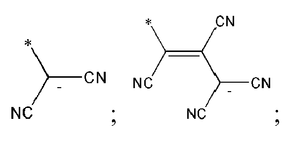
- L101 may be a C5-C14 arylene group; a C5-C14 heteroarylene group; or a substituted C2-C10 alkenylene group, a substituted C5-C14 arylene group, or a substituted C5-C14 heteroarylene group which have at least one substituent that is a halogen atom, a cyano group, a hydroxyl group, a C1-C10 alkyl group, or a C1-C10 alkoxy group.
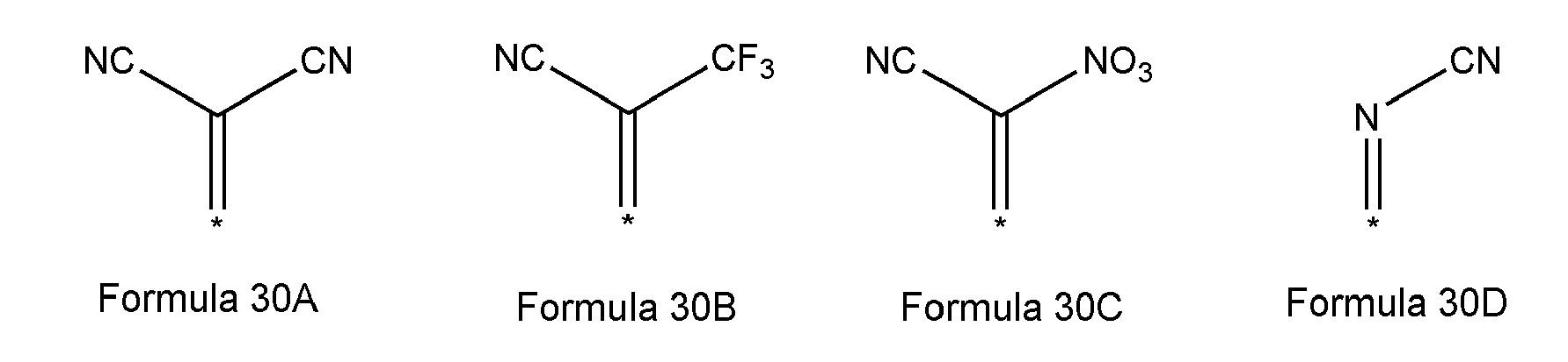
- X1 through X4 may each independently be the compound represented by Formula 30A or the compound represented by Formula 30D.
- R103 may be hydrogen; a halogen atom; a cyano group; a C1-C10alkyl group; a C1-C10 alkoxy group; a substituted C1-C10 alkyl group or a substituted C1-C10 alkoxy group which have at least one substituent that is a halogen atom, a cyano group, a phenyl group, a naphthyl group, an anthryl group, a pyridinyl group, a thiophenyl group, or a benzothiophenyl group; or -N(R107)(R108), wherein R107 and R108 may each independently be hydrogen, a C1-C10 alkyl group, a phenyl group, or a biphenyl group.
- T1 and T2 may each independently be benzene; naphthalene; anthracene; thiophene; thiadiazole; oxadiazole; or a substituted benzene, a substituted naphthalene, a substituted anthracene, a substituted thiophene, a substituted thiadiazole, or a substituted oxadiazole which have at least one substituent that is a halogen atom, a cyano group, a C1-C10 alkyl group, or a C1-C10 alkoxy group.
- L101 may be a thiophenylene group; a benzothiophenylene group; or a substituted thiophenylene group or a substituted benzothiophenylene group which have at least one substituent that is a halogen atom, a cyano group, or a C1-C10 alkyl group.
- The cyano group-containing compound may be one represented by Formulae 1A through 20B.
- In Formulae 1A through 20B, R103 and R109 may each independently be a hydrogen atom, -F, a cyano group, a methyl group, an ethyl group, a propyl group, a ethenyl group, a methoxy group, an ethoxy group, or a propoxy group.
- The layer may further include a hole transporting compound.
- The hole transporting compound may be one represented by Formula 41 or 42.
- In Formulae 41 and 42,
- R10 may be represented by -(Ar1)n-Ar2;
- R16 may be represented by -(Ar11)m-Ar12;
- Ar1, Ar11, L1, and L11 may each independently be a substituted or unsubstituted C1-C30 alkylene group, a substituted or unsubstituted C2-C30 alkenylene group, a substituted or unsubstituted C5-C30 arylene group, a substituted or unsubstituted C4-C30 heteroarylene group, or -N(Q1)-;
- n, m, a, and b may each independently be an integer from 0 to 10;
- R1 through R3, R11 through R15, R17, R18, R21 through R29, Ar2, Ar12, and Q1 may each independently be hydrogen, a halogen atom, a hydroxyl group, a cyano group, a substituted or unsubstituted C1-C30alkyl group, a substituted or unsubstituted C2-C30 alkenyl group, a substituted or unsubstituted C2-C30 alkynyl group, a substituted or unsubstituted C1-C30 alkoxy group, a substituted or unsubstituted C1-C30 alkylthiol group, a substituted or unsubstituted C5-C30 aryl group, a C4-C30 heteroaryl group, or -N(Q2)(Q3);
- Q2 and Q3 may each independently be hydrogen, a halogen atom, a hydroxyl group, a cyano group, a substituted or unsubstituted C1-C30 alkyl group, a substituted or unsubstituted C2-C30 alkenyl group, a substituted or unsubstituted C2-C30 alkynyl group, a substituted or unsubstituted C1-C30 alkoxy group, a substituted or unsubstituted C1-C30 alkylthiol group, a substituted or unsubstituted C5-C30 aryl group, or a substituted or unsubstituted C4-C30 heteroaryl group; and
- n groups of Ar1 in -(Ar1)n- may be identical to or different from each other, m groups of Ar11 in -(Ar11)m- may be identical to or different from each other, a groups of L1 in -(L1)a-may be identical to or different from each other, and b groups of L11 in -(L11)b- may be identical to or different from each other.
- Ar1 and Ar11 may each independently be a C1-C10 alkylene group; a phenylene group; a naphthylene group; an anthrylene group; a fluorenylene group; a carbazolylene group; a pyrazolylene group; a pyridinylene group; a triazinylene group; -N(Q1)-; or a substituted C1-C10 alkylene group, a substituted phenylene group, a substituted naphthylene group, a substituted anthrylene group, a substituted fluorenylene group, a substituted carbazolylene group, a substituted pyrazolylene group, a substituted pyridinylene group, or a substituted triazinylene group which have at least one substituent that is halogen atom, a cyano group, a hydroxyl group, a C1-C10 alkyl group, a C1-C10 alkoxy group, a phenyl group, a naphthyl group, or an anthryl group; and
- Q1 may be hydrogen; a C1-C10 alkyl group; a phenyl group; a naphthyl group; a carbazolyl group; a fluorenyl group; or a substituted C1-C10 alkyl group, a substituted C1-C10alkoxy group, a substituted phenyl group, a substituted naphthyl group, a substituted carbazolyl group, or a substituted fluorenyl group which have at least one substituent that is a halogen atom, a cyano group, a hydroxyl group, a C1-C10 alkyl group, a C1-C10 alkoxy group, a phenyl group, a naphthyl group, or an anthryl group.
- Ar2 and Ar12 may each independently be hydrogen; a C1-C10 alkyl group; a phenyl group; a naphthyl group; a carbazolyl group; a fluorenyl group; a pyrenyl group; a substituted C1-C10 alkyl group, a substituted C1-C10 alkoxy group, a substituted phenyl group, a substituted naphthyl group, a substituted carbazolyl group, a substituted fluorenyl group, or a substituted pyrenyl group which have at least one substituent that is a halogen atom, a cyano group, a hydroxyl group, a C1-C10 alkyl group, a C1-C10 alkoxy group, a phenyl group, a naphthyl group, or an anthryl group; or -N(Q2)(Q3), wherein Q2 and Q3 may each independently be hydrogen, a methyl group, an ethyl group, a phenyl group, a methylphenyl group, a biphenyl group, a naphthyl group, or a methylnaphthyl group. The amount of the cyano group-containing compound in the layer may be 0.1 to 20 parts by weight, based on 100 parts by weight of the first layer.
- The layer may have a thickness of 10 Å to 2,100 Å.
- A distance between the layer and the emission layer may be 50 Å or greater.
- The electron transport layer may include an anthracene-based compound and a quinolate-based compound.
- The anthracene-based compound may be one represented by Formula 101 and Formula 102, and the quinolate-based compound may be lithium quinolate (LiQ).
- In Formulae 101 and 102,
- R*1 through R*6 may each independently be a hydrogen atom, a halogen atom, a hydroxy group, a cyano group, a substituted or unsubstituted C1-C30 alkyl group, a substituted or unsubstituted C1-C30 alkoxy group, a substituted or unsubstituted C1-C30 acyl group, a substituted or unsubstituted C2-C30 alkenyl group, a substituted or unsubstituted C2-C30 alkynyl group, a substituted or unsubstituted C6-C30 aryl group, or a substituted or unsubstituted C3-C30 heteroaryl group, wherein at least two adjacent groups of R*1 through R*6 are linked to form a saturated or unsaturated ring;
- L*1 may be a single bond, a substituted or unsubstituted C1-C30 alkylene group, a substituted or unsubstituted C6-C30 arylene group, or a substituted or unsubstituted C3-C30 hetero arylene group;
- Q*1 through Q*9 may each independently be a hydrogen atom, a substituted or unsubstituted C6-C30 aryl group, or a substituted or unsubstituted C3-C30 heteroaryl group; and
- a* may be an integer from 1 to 10.
- The anthracene-based compound may also be one represented by Formula 103 and Formula 104, and the quinolate-based compound may be lithium quinolate (LiQ).
- The amount of the anthracene-based compound may be 50 to 150 parts by weight, based on 100 parts by weight of the quinolate-based compound.
- The emission layer may include a blue dopant and a blue host.
- The emission layer may include a blue dopant represented by Formula 201 and a blue host represented by Formula 202.
- In Formulae 201 and 202,
- L21 may be a substituted or unsubstituted C1-C30 alkylene group, a substituted or unsubstituted C2-C30 alkenylene group, a substituted or unsubstituted C5-C30 arylene group, or a substituted or unsubstituted C4-C30 heteroarylene group;
- c may be an integer from 1 to 20;
- R31 through R34 may each independently be a substituted or unsubstituted C1-C30 alkyl group, a substituted or unsubstituted C2-C30 alkenyl group, a substituted or unsubstituted C2-C30 alkynyl group, a substituted or unsubstituted C1-C30 alkoxy group, a substituted or unsubstituted C5-C30 aryl group, or a substituted or unsubstituted C4-C30 heteroaryl group.
- c groups of L21 in -(L21)c- may be identical to or different from each other;
- Ar51, A52, Ar53, and Ar54 may each independently be a phenylene group, a naphthylene group, an anthrylene group, or a phenyl-substituted anthrylene group,
- R51 through R56 may each independently be a hydrogen atom, a methyl group, an ethyl group, a propyl group, a butyl group, a phenyl group, a naphthyl group, an anthryl group, a pyrenyl group, a carbazolyl group, or -N(Q2)(Q3), wherein Q2 and Q3 may each independently be a methyl group, a phenyl group, a naphthyl group, or an anthryl group; and
- d, e, f, and g may each independently be an integer from 0 to 10.
- The above and other features and advantages will become more apparent to those of skill in the art by describing in detail example embodiments with reference to the attached drawing, in which:
-
FIG. 1 illustrates a cross-sectional view of a structure of an organic light-emitting device (OLED) according to an embodiment. - Example embodiments will now be described more fully hereinafter with reference to the accompanying drawing.
- In the drawing figure, the dimensions of layers and regions are exaggerated for clarity of illustration. It will also be understood that when a layer or element is referred to as being "on" another layer or substrate, it can be directly on the other layer or substrate, or intervening layers may also be present. Further, it will be understood that when a layer is referred to as being "under" another layer, it can be directly under, and one or more intervening layers may also be present. In addition, it will also be understood that when a layer is referred to as being "between" two layers, it can be the only layer between the two layers, or one or more intervening layers may also be present. Like reference numerals refer to like elements throughout.
-
FIG. 1 illustrates a schematic cross-sectional view of a structure of an organic light-emitting device (OLED) 10 according to an embodiment. Referring toFIG. 1 , theOLED 10 according to an embodiment may include asubstrate 1, afirst electrode 5, alayer 6, anorganic layer 7, and asecond electrode 9 sequentially stacked in the stated order. Thefirst layer 6 may include a cyano group-containing compound. Theorganic layer 7 may include an emission layer (EML) and an electron transport layer (ETL). - The
substrate 1 is a suitable substrate that is used in conventional organic light-emitting devices. Thesubstrate 1 may be, e.g., a glass substrate or a transparent plastic substrate providing one or more of mechanical strength, thermal stability, transparency, surface smoothness, ease of handling, and water resistance. - The
first electrode 5 may constitute an anode or a cathode. Examples of the first electrode material include materials, such as indium tin oxide (ITO), indium zinc oxide (IZO), tin oxide (SnO2), zinc oxide (ZnO), aluminum (Al), silver (Ag), and magnesium (Mg), which have excellent conductivity. The first electrode material may form a transparent or reflective electrode. - The
layer 6 may include a cyano group-containing compound and is disposed on thefirst electrode 5. The cyano group-containing compound included in thelayer 6 has two one-electron reduced forms, and may have an extended π-electron system capable of generating stable radicals (this can be identified by, e.g., cyclic voltammetry). Thelayer 6 may lower a barrier of hole injection from thefirst electrode 5 into theorganic layer 7. Thus, thelayer 6 may facilitate the injection of holes into theorganic layer 7 from thefirst electrode 5. Thus, theOLED 10 may have excellent driving voltage characteristics and power efficiency characteristics. - The cyano group-containing compound included in the
layer 6 may be one of the compounds represented byFormulae 1 through 20 below.


- In Formulae 1 through 20, X1 through X4 are each independently be compounds represented by Formulae 30A through 30D below; Y1 through Y8 are each independently be N or C(R103); Z1 through Z4 are each independently be C or N; A1 and A2 are each independently be -O-, -S-, -N(R104) or -C(R105)(R106)-; Q101 and Q102 are each independently be a C2-C10 alkylene group, a C2-C10alkenylene group, or a substituted C2-C10alkylene group or a substituted C2-C10 alkenylene group which have at least one substituent that is a halogen atom, a cyano group, a hydroxyl group, a C1-C10 alkyl group or a C1-C10 alkoxy group; T1 and T2 are each independently be a C5-C30 aromatic ring system, a C2-C30 heteroaromatic ring system, or a substituted C5-C30 aromatic ring system or a substituted C2-C30 heteroaromatic ring system which have at least one substituent that is a halogen atom, a cyano group, a hydroxyl group, a C1-C10 alkyl group or a C1-C10 alkoxy group; p is an integer from 1 to 10; q is an integer from 0 to 10; R101 through R106 are each independently be hydrogen, a halogen atom, a cyano group, a hydroxyl group, a C1-C10 alkyl group, a C1-C10 alkoxy group, a substituted C1-C10 alkyl group or a substituted C1-C10 alkoxy group which have at least one substituent that is a halogen atom, a cyano group, a hydroxyl group, a C5-C14 aryl group, or a C2-C14 heteroaryl group,

- For example, in
Formula 1 through 20, X1 through X4 may each independently be a compound represented by Formula 30A or a compound represented by Formula 30D. - For example, R103 in C(R103) for Y1 through Y8 in
Formulae 1 through 20 may be hydrogen; a halogen atom; a cyano group; a C1-C10alkyl group; a C1-C10alkoxy group; a substituted C1-C10alkyl group or a substituted C1-C10alkoxy group which have at least one substituent that is a halogen atom, a cyano group, a phenyl group, a naphthyl group, an anthryl group, a pyridinyl group, a thiophenyl group, or a benzothiophenyl group; or -N(R107)(R108), wherein R107 and R108 may each independently be hydrogen, a C1-C10 alkyl group, a phenyl group, or a biphenyl group. - In particular, R103 may be hydrogen, -F, a cyano group, a methyl group, an ethyl group, a propyl group, an ethenyl group, a methoxy group, an ethoxy group, a propoxy group, a phenyl-substituted methyl group, a phenyl-substituted propyl group, or an -N(biphenyl group)(biphenyl group).
- In
Formulae 1 and 2, R101 and R102 may each independently be a cyano group,

- In
Formulae 1 through 20, A1 and A2 may be -S-. - In Formula 20, Q101 and Q102 may each independently be an ethylene group, a propylene group, an ethenylene group, a propylene group, or a substituted ethylene group, a substituted propylene group, a substituted ethenylene group, or a substituted propylene group which have at least one substituent that is a halogen atom, a cyano group, or a hydroxyl group. In particular, Q101 and Q102 may each independently be an ethylene group, an ethenylene group, or a substituted ethylene group or a substituted ethenylene group which have at least one substituent that is -F or a cyano group.
- In
Formulae 1 through 20, T1 and T2 may each independently be a C5-C30aromatic ring system including elements Z1 and Z2, or Z3 and Z4; a C2-C30 heteroaromatic ring system; a substituted C5-C30 aromatic ring system having at least one substituent that is a halogen atom, a cyano group, a hydroxyl group, a C1-C10alkyl group, or a C1-C10alkoxy group; or a substituted C5-C30 heteroaromatic ring system having at least one substituent that is a halogen atom, a cyano group, a hydroxyl group, a C1-C10alkyl group, or a C1-C10 alkoxy group. In an implementation, T1 and T2 may each independently be a C6-C30aromatic ring system including elements Z1 and Z2, or Z3 and Z4; a C2-C30heteroaromatic ring system; a substituted C6-C30aromatic ring system having at least one substituent that is a halogen atom, a cyano group, a hydroxyl group, a C1-C10alkyl group, or a C1-C10alkoxy group; or a substituted C5-C30heteroaromatic ring system having at least one substituent that is a halogen atom, a cyano group, a hydroxyl group, a C1-C10alkyl group, or a C1-C10 alkoxy group. As identified fromFormulae 1 through 20, T1 and T2 are fused to the backbones ofFormulae 1 through 20. - The C5-C30 aromatic ring system refers to a C5-C30 carbocyclic aromatic system including at least one aromatic ring. In this regard, the term "system" used herein indicates that the C5-C30 aromatic ring system may include a polycyclic structure. When the C5-C30 aromatic ring system includes 2 or more aromatic rings, the 2 or more aromatic rings may be fused together. The C2-C30 heteroaromatic ring system refers to a C2-C30 carbocyclic aromatic system including at least one heteroaromatic ring, wherein the at least one heteroaromatic ring includes at least one heteroatom that is nitrogen (N), oxygen (O), phosphorous (P) or sulfur (S), and has carbon (C) as the other ring atoms. When the C2-C30 heteroaromatic ring system further includes at least one of an aromatic ring group and a heteroaromatic ring, two or more (hetero)aromatic rings may be fused together.
- Examples of the C5-C30 aromatic ring system include benzene, pentalene, indene, naphthalene, azulene, heptalene, indacene, acenaphthylene, fluorene, phenalene, phenanthrene, anthracene, fluoranthene, triphenylene, pyrene, chrysene, naphthacene, picene, perylene, pentaphene, and hexacene.
- Examples of the C5-C30 heteroaromatic ring system include pyrrole, pyrazole, imidazole, imidazoline, pyridine, pyrazine, pyrimidine, indole, purine, quinoline, phthalazine, indolizine, naphthyridine, quinazoline, cinnoline, indazole, carbazole, phenazine, phenanthridine, pyran, chromene, benzofuran, thiophene, benzothiophene, isothiazole, isoxazole, thiadiazole, and oxadiazole.
- For example, in
Formulae 1 through 20, T1 and T2 may each independently be benzene; naphthalene; anthracene; thiophene; thiadiazole; oxadiazole; or a substituted benzene, a substituted naphthalene, a substituted anthracene, a substituted thiophene, a substituted thiadiazole, or a substituted oxadiazole which have at least one substituent that is a halogen atom, a cyano group, a C1-C10 alkyl group, or a C1-C10 alkoxy group. - In
Formulae 1 through 20, p may be 1. In addition, q may be 0, 1, or 2. For example, when q in Formula 3 is 0, the compound represented by Formula 3 may be a compound represented by Formula 3A, which will be described below. - In Formula 2, L101 may be a C5-C14 arylene group; a C5-C14 heteroarylene group; a substituted C5-C14 arylene group having at least one substituent that is a halogen atom, a cyano group, a hydroxyl group, a C1-C10alkyl group or a C1-C10 alkoxy group; or a substituted C5-C14 heteroarylene group having at least one substituent that is a C2-C10 alkenylene group, a halogen atom, a cyano group, a hydroxyl group, a C1-C10 alkyl group, or a C1-C10 alkoxy group. In an implementation, L101 may be a C6-C14 arylene group; a C5-C14 heteroarylene group; a substituted C6-C14 arylene group having at least one substituent that is a halogen atom, a cyano group, a hydroxyl group, a C1-C10 alkyl group or a C1-C10 alkoxy group; or a substituted C5-C14 heteroarylene group having at least one substituent that is a C2-C10 alkenylene group, a halogen atom, a cyano group, a hydroxyl group, a C1-C10 alkyl group, or a C1-C10 alkoxy group. For example, L101 may be a thiophenylene group; a benzothiophenylene group; or a substituted thiophenylene group or a substituted benzothiophenylene group which have at least one substituent that is a halogen atom, a cyano group, or a C1-C10 alkyl group.
- One or more of the compounds represented by Formulae 1A through 20B, below, may be used for the cyano group-containing compound included in the
layer 6 of the OLED 10:

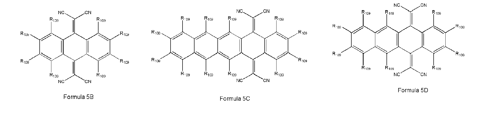
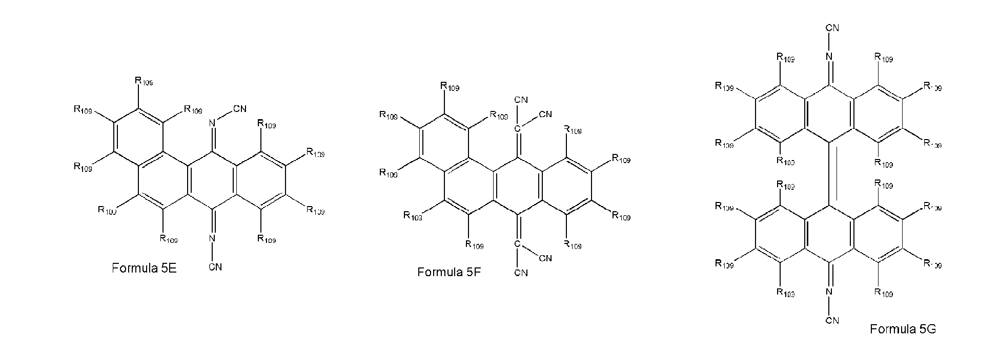
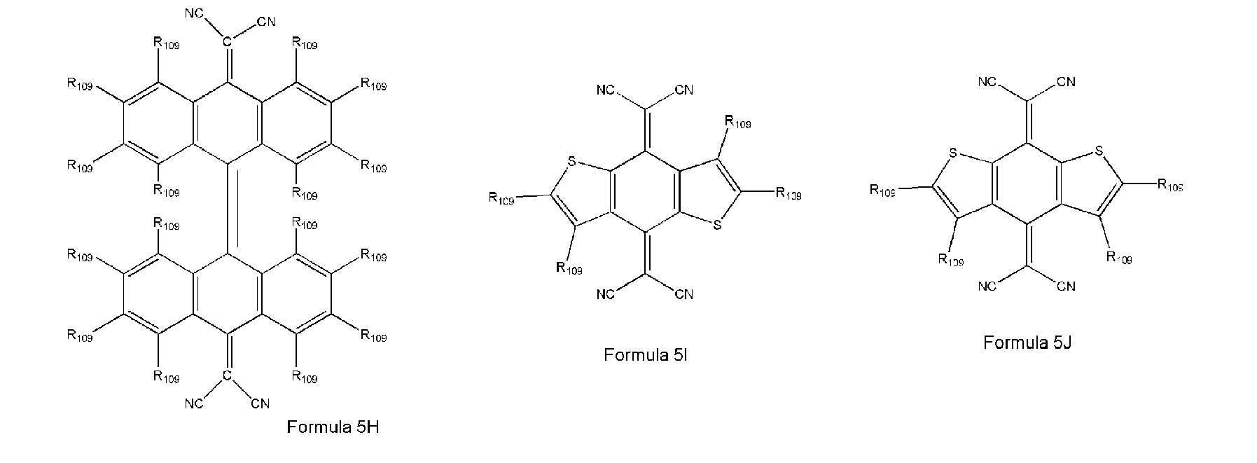


- In Formulae 1A through 20B, R103 and R109 may each independently be a hydrogen atom, -F, a cyano group, a methyl group, an ethyl group, a propyl group, a methoxy group, an ethoxy group, or a propoxy group.
- For example, the compound represented by Formula 20A or 20B may be the cyano group-containing compound included in the
layer 6 of theOLED 10. In Formulae 20A and 20B, R103 and R109 may both be -F. - The cyano group-containing compound included in the
layer 6 improves the hole injecting ability of thefirst electrode 5. Thus, theOLED 10 has a reduced driving voltage and higher emission and power efficiencies. - The
layer 6 may include a hole transporting compound in addition to the cyano group-containing compound described above. The cyano group-containing compound may form a charge transfer complex with the hole transporting compound, so that the concentration of free carriers in thelayer 6 may be increased. Thus, the cyano group-containing compound may contribute to a reduction in interfacial resistance between thefirst electrode 5 and theorganic layer 7. - One or more of the compounds represented by Formulae 41 and 42, below, may be used for the hole transporting compound:


- In Formulae 41 and 42, R10 may be represented by -(Ar1)n-Ar2; R16 may be represented by -(Ar11)m-Ar12; Ar1, Ar11, L1 and L11 may each independently be a substituted or unsubstituted C1-C30alkylene group, a substituted or unsubstituted C2-C30 alkenylene group, a substituted or unsubstituted C5-C30 arylene group, a substituted or unsubstituted C4-C30 heteroarylene group, or a group represented by -N(Q1)-; n, m, a, and b may each independently be an integer from 0 to 10; R1 through R3, R11 through R15, R17, R18, R21 through R29, Ar2, Ar12, and Q1 may each independently be hydrogen, a halogen atom, a hydroxyl group, a cyano group, a substituted or unsubstituted C1-C30 alkyl group, a substituted or unsubstituted C2-C30 alkenyl group, a substituted or unsubstituted C2-C30 alkynyl group, a substituted or unsubstituted C1-C30 alkoxy group, a substituted or unsubstituted C1-C30 alkylthiol group, a substituted or unsubstituted C5-C30 aryl group, a substituted or unsubstituted C4-C30 heteroaryl group, or a group represented by -N(Q2)(Q3); and Q2 and Q3 may each independently be hydrogen, a halogen atom, a hydroxyl group, a cyano group, a substituted or unsubstituted C1-C30 alkyl group, a substituted or unsubstituted C2-C30 alkenyl group, a substituted or unsubstituted C2-C30 alkynyl group, a substituted or unsubstituted C1-C30 alkoxy group, a substituted or unsubstituted C1-C30 alkylthiol group, a substituted or unsubstituted C5-C30 aryl group, or a substituted or unsubstituted C4-C30 heteroaryl group, wherein n groups of Ar1 in -(Ar1)n-may be identical to or different from each other, m groups of Ar11 in -(Ar11)m- may be identical to or different from each other, a groups of L1 in -(L1)a- may be identical to or different from each other, and b groups of L11 in -(L11)b- may be identical to or different from each other. In an implementation, L1 and L11 may each independently be a substituted or unsubstituted C1-C30 alkylene group, a substituted or unsubstituted C2-C30 alkenylene group, a substituted or unsubstituted C6-C30 arylene group, a substituted or unsubstituted C4-C30 heteroarylene group, or a group represented by -N(Q1)-; R1 through R3, R11 through R15, R17, R18, R21 through R29, Ar2, Ar12 and Q1 may each independently be hydrogen, a halogen atom, a hydroxyl group, a cyano group, a substituted or unsubstituted C1-C30 alkyl group, a substituted or unsubstituted C2-C30 alkenyl group, a substituted or unsubstituted C2-C30 alkynyl group, a substituted or unsubstituted C1-C30 alkoxy group, a substituted or unsubstituted C1-C30 alkylthiol group, a substituted or unsubstituted C6-C30 aryl group, a substituted or unsubstituted C4-C30 heteroaryl group, or a group represented by -N(Q2)(Q3); and Q2 and Q3 may each independently be hydrogen, a halogen atom, a hydroxyl group, a cyano group, a substituted or unsubstituted C1-C30 alkyl group, a substituted or unsubstituted C2-C30 alkenyl group, a substituted or unsubstituted C2-C30 alkynyl group, a substituted or unsubstituted C1-C30 alkoxy group, a substituted or unsubstituted C1-C30 alkylthiol group, a substituted or unsubstituted C6-C30 aryl group, or a substituted or unsubstituted C4-C30 heteroaryl group.
- Examples of Ar1 in the formula -(Ar1)n-Ar2- for R10 and Ar11 in the formula -(Ar11)m-Ar12-for R16 may each independently be a substituted or unsubstituted C1-C10 alkylene group, a substituted or unsubstituted C2-C10 alkenylene group, a substituted or unsubstituted phenylene group, a substituted or unsubstituted pentalenylene group, a substituted or unsubstituted indenylene group, a substituted or unsubstituted naphthylene group, a substituted or unsubstituted azulenylene group, a substituted or unsubstituted heptalenylene group, a substituted or unsubstituted indacenylene group, a substituted or unsubstituted acenaphthylene group, a substituted or unsubstituted fluorenylene group, a substituted or unsubstituted phenalenylene group, a substituted or unsubstituted phenanthrenylene group, a substituted or unsubstituted anthracenylene group, a substituted or unsubstituted fluoranthenylene group, a substituted or unsubstituted triphenylenylene group, a substituted or unsubstituted pyrenylenylene group, a substituted or unsubstituted chrysenylene group, a substituted or unsubstituted perylenylene group, a substituted or unsubstituted pyrrolylene group, a substituted or unsubstituted pyrazolylene group, a substituted or unsubstituted imidazolylene group, a substituted or unsubstituted imidazolinylene group, a substituted or unsubstituted imidazopyridinylene group, a substituted or unsubstituted imidazopyrimidinylene group, a substituted or unsubstituted pyridinylene group, a substituted or unsubstituted pyrazinylene group, a substituted or unsubstituted pyrimidinylene group, a substituted or unsubstituted indolylene group, a substituted or unsubstituted purinylene group, a substituted or unsubstituted quinolinylene group, a substituted or unsubstituted phthalazinylene group, a substituted or unsubstituted indolizinylene group, a substituted or unsubstituted naphthyridinylene group, a substituted or unsubstituted quinazolinylene group, a substituted or unsubstituted cinnolinylene group, a substituted or unsubstituted indazolylene group, a substituted or unsubstituted carbazolylene group, a substituted or unsubstituted phenazinylene group, a substituted or unsubstituted phenanthridinylene group, a substituted or unsubstituted pyranylene group, a substituted or unsubstituted chromenylene group, a substituted or unsubstituted benzofuranylene group, a substituted or unsubstituted thiophenylene group, a substituted or unsubstituted benzothiophenylene group, a substituted or unsubstituted isothiazolylene group, a substituted or unsubstituted benzoimidazolylene group, a substituted or unsubstituted isoxazolylene group, a substituted or unsubstituted triazinylene group, or a group represented by -N(Q1)-, but are limited thereto. In this regard, Q1 may be hydrogen, a halogen atom, a hydroxyl group, a cyano group, a substituted or unsubstituted C1-C10 alkyl group, a substituted or unsubstituted C2-C10 alkenyl group, a substituted or unsubstituted C2-C10 alkynyl group, a substituted or unsubstituted C1-C10 alkoxy group, a substituted or unsubstituted C1-C10 alkylthiol group, a substituted or unsubstituted C5-C14 aryl group, a substituted or unsubstituted C4-C14 heteroaryl group, or -N(Q2)(Q3). In an implementation, Q1 may be hydrogen, a halogen atom, a hydroxyl group, a cyano group, a substituted or unsubstituted C1-C10 alkyl group, a substituted or unsubstituted C2-C10 alkenyl group, a substituted or unsubstituted C2-C10 alkynyl group, a substituted or unsubstituted C1-C10 alkoxy group, a substituted or unsubstituted C1-C10 alkylthiol group, a substituted or unsubstituted C6-C14 aryl group, a substituted or unsubstituted C4-C14 heteroaryl group, or -N(Q2)(Q3).
- For example, Ar1 and Ar11 may each independently be a C1-C10 alkylene group; a phenylene group; a naphthylene group; an anthrylene group; a fluorenylene group; a carbazolylene group; a pyrazolylene group; a pyridinylene group; a triazinylene group; -N(Q1)-; or a substituted C1-C10 alkylene group, a substituted phenylene group, a substituted naphthylene group, a substituted anthrylene group, a substituted fluorenylene group, a substituted carbazolylene group, a substituted pyrazolylene group, a substituted pyridinylene group, or a substituted triazinylene group which have at least one substituent that is a halogen atom, a cyano group, a hydroxyl group, a C1-C10 alkyl group, a C1-C10 alkoxy group, a phenyl group, a naphthyl group, or an anthryl group. In this regard, Q1 may be hydrogen; a C1-C10 alkyl group; a phenyl group; a naphthyl group; a carbazolyl group; a fluorenyl group; a pyrenyl group; a substituted C1-C10 alkyl group, a substituted C1-C10 alkoxy group, a substituted phenyl group, a substituted naphthyl group, a substituted carbazolyl group, a substituted fluorenyl group, or a substituted pyrenyl group which have at least one substituent that is a halogen atom, a cyano group, a hydroxyl group, a C1-C10 alkyl group, a C1-C10 alkoxy group, a phenyl group, a naphthyl group, or an anthryl group; or -N(Q2)(Q3). In addition, Q2 and Q3 may be a methyl group, a phenyl group, a naphthyl group, or an anthryl group.
- Ar2 in the formula -(Ar1)n-Ar2- and Ar12 in the formula -(Ar11)m-Ar12- are as defined above in connection with Q1.
- Also, n in the formula -(Ar1)n-Ar2- and m in the formula -(Ar11)m-Ar12- may each independently be an integer from 0 to 10. For example, n and m may each independently be 0, 1, 2, 3, 4, or 5.
- Also, n groups of Ar1 in the formula -(Ar1)n-Ar2- may be identical to or different from each other. For example, when n is 2, the two groups of Ar1 in -(Ar1)n- may both be phenylene groups, or one of the two may be -N(Q1)- and the other may be a phenylene group. The descriptions of -(Ar11)m-Ar12- may be the same as those of -(Ar1)n-Ar2-above.
- R1 through R3, R11 through R15, R17, R18, and R21 through R29 in Formulae 41 and 42 may be defined as described above in connection with Q1.
- For example, R13 may be a phenyl group, a naphthyl group, or an anthryl group.
- For example, R28 and R29 may each independently be a hydrogen atom, a methyl group, an ethyl group, a methoxy group, an ethoxy group, a phenyl group, a naphthyl group, or an anthryl group.
- L1 and L2 in Formulae 41 and 42 may be defined as described above in connection with Ar1 and Ar11.
- For example, L1 and L2 may each independently be a phenylene group, a carbazolylene group, or a phenylcarbazolylene group.
- In Formulae 41 and 42, a and b may each independently be an integer from 0 to 10. For example, a and b may each independently be 0, 1, 2, or 3.
- For example, in Formula 42, Ar1 in the formula -(Ar1)n-Ar2- for R10 and Ar11 in the formula -(Ar11)m-Ar12- for R16 may each independently be a phenylene group; a carbazolylene group; a fluorenylene group; a methylfluorenylene group; a pyrazolylene group; a phenylpyrazolylene group; -N(Q1)-, wherein Q1 is hydrogen, a phenyl group, a fluorenyl group, a dimethylfluorenyl group, a diphenylfluorenyl group, a carbazolyl group, or a phenylcarbazolyl group; a diphenylfluorenylene group; a triazinylene group; a methyltriazinylene group; a phenyltriazinylene group; a tetrafluorophenylene group; an ethylene group; or a methylphenylene group, wherein n and m may each independently be 0, 1, 2, 3, 4, 5 or 6, and Ar2 and Ar12 may each independently be hydrogen, a cyano group, a fluoro group, a phenyl group, a cyanophenyl group, a naphthyl group, an anthryl group, a methyl group, a pyridinyl group, a carbazolyl group, a phenylcarbazolyl group, a fluorenyl group, a dimethylfluorenyl group, or a diphenylfluorenyl group. R11, R12, R14, R15, R17, R18, R21 through R27 may be hydrogen; R13 may be a phenyl group, a naphthyl group, or an anthryl group; R28 and R29 may each independently be hydrogen, a methyl group, an ethyl group, a methoxy group, an ethoxy group, a phenyl group, a naphthyl group, or an anthryl group; L11 may be a phenylene group; and b may be 0 or 1. In an embodiment, one or more of
Compounds 1 through 37 below may be used for the hole transporting compound:


- When the
layer 6 includes a hole transporting material described above in addition to the cyano group-containing compound, the amount of the cyano group-containing compound in thelayer 6 may be 0.1 to 20 parts by weight, for example, 0.5 to 15 parts by weight, or 0.5 to 10 parts by weight, based on 100 parts by weight of thelayer 6. With such an amount of the cyano group-containing compound, the driving voltage may be satisfactorily decreased, and the emission and power efficiencies can be satisfactorily improved. - The thickness of the
layer 6 may be 10 Å to 2,100 Å, for example, 10 Å to 500 Å, or 20 Å to 200 Å. With such a thickness of thelayer 6, the driving voltage may be satisfactorily decreased, and the emission and power efficiencies can be satisfactorily improved. - The
organic layer 7 is disposed on thelayer 6. The term "organic layer" used throughout the specification refers to any intervening layer between thefirst electrode 5 and the second electrode 9 (but excluding thelayer 6 described above). Theorganic layer 7 is formed of organic materials, and may further include a metal complex. - The
organic layer 7 include a hole transprot layer (HTL), an emission layer (EML) and an electron transport layer (ETL). - A distance between the
layer 6 and the EML may be 50 Å or greater, for example, 100 Å or greater, or 100 Å to 2,500 Å. With such a distance between thelayer 6 and the EML, quenching of excitons in the emission layer caused by the cyano group-containing compound included in thelayer 6 can be substantially prevented. Thus, the OLED has excellent quality. - The
organic layer 7 may further include at least one of a hole injection layer (HIL), a hole blocking layer (HBL), and an electron injection layer (EIL), in addition to the EML and the ETL. - The HIL may be further disposed between the
layer 6 and the EML.. - The HIL may be formed on the
layer 6 by vacuum deposition, spin coating, casting, Langmuir-Blodgett (LB) deposition, or the like. - When the HIL is formed using vacuum deposition, the deposition conditions may vary according to a compound that is used to form the HIL, and the structure and thermal properties of the HIL to be formed. In general, however, conditions for vacuum deposition may include a deposition temperature of 100 to 500 °C, a pressure of 10-8 to 10-3 torr, and a deposition rate of 0.01 to 100 Å/sec.
- When the HIL is formed using spin coating, the coating conditions may vary according to a compound that is used to form the HIL, and the structure and thermal properties of the HIL to be formed. In general, however, the coating rate may be in the range of 2,000 to 5,000 rpm, and a temperature for heat treatment which is performed to remove a solvent after coating may be in the range of 80 to 200 °C.
- Examples of the material that can be used to form the HIL include a phthalocyanine compound such as copper phthalocyanine, 4,4',4"-tris(3-methylphenylphenylamino) triphenylamine (m-MTDATA), N,N'-di(1-naphthyl)-N,N'-diphenylbenzidine (NPB), TDATA, 2T-NATA, polyaniline/dodecylbenzenesulfonic acid (Pani/DBSA), poly(3,4-ethylenedioxythiophene)/poly(4-styrenesulfonate) (PEDOT/PSS), polyaniline/camphor sulfonic acid (Pani/CSA), and polyaniline)/poly(4-styrenesulfonate (PANI/PSS).

- The thickness of the HIL may be about 50 to 1,000 Å, for example, about 100 to about 2,500 Å. With such a thickness of the HIL, the HIL may have excellent hole injecting ability without a substantial increase in driving voltage.
- Then, the HTL may be formed directly on the HIL or directly on the
layer 6 by vacuum deposition, spin coating, casting, Langmuir-Blodgett (LB) deposition, or the like. When the HTL is formed using vacuum deposition or spin coating, the conditions for deposition and coating may be similar to those for the formation of the HIL, although the conditions for the deposition and coating may vary according to the material that is used to form the HTL. - One or more of the compounds represented by Formula 41 or 42 described above may be used to form the HTL.
- The thickness of the HTL may be about 50 to 1,000 Å, for example, about 100 to about 2,500 Å. With such a thickness of the HTL, the HTL may have a satisfactory hole transporting ability without a substantial increase in driving voltage.
- Then, the EML may be formed on the HTL by using vacuum deposition, spin coating, casting, LB deposition, or the like. When the EML is formed using vacuum deposition or spin coating, the conditions for deposition and coating may be similar to those for the formation of the HIL, although the conditions for deposition and coating may vary according to the material that is used to form the EML.
- The EML may include a blue dopant and a blue host.
- The blue host may be a compound represented by Formula 202 below. Examples of the blue host may include 9,10-di-(2-naphthyl) anthracene (ADN), 2-methyl-9,10-di-(2-naphthyl) anthracene (MADN), 2-tert-butyl-9,10-bis(β-naphthyl)-anthracene (TBADN), and 9,10,10-tetraphenyl-2,2-bianthracene (TPBA).

- In Formula 202, Ar51, A52, Ar53 and Ar54 may each independently be a phenylene group, a naphthylene group, an anthrylene group, or a phenyl-substituted anthrylene group.
- R51 through R56 may each independently be a hydrogen atom, a methyl group, an ethyl group, a propyl group, a butyl group, a phenyl group, a naphthyl group, an anthryl group, a pyrenyl group, a carbazolyl group, or -N(Q2)(Q3), wherein Q2 and Q3 are each independently a methyl group, a phenyl group, a naphthyl group, or an anthryl group.
- In Formula 202, d, e, f, and g may each independently be an integer from 0 to 10. For example, d, e, f, and g may each independently be 0, 1, or 2.
- The blue dopant may be a compound represented by Formula 201. For example, the blue dopant may be a compound represented by Formula 203 or 204.


- R35 and R42 may each independently be hydrogen, a halogen atom, a hydroxyl group, a cyano group, a substituted or unsubstituted C1-C30 alkyl group, a substituted or unsubstituted C2-C30 alkenyl group, a substituted or unsubstituted C2-C30 alkynyl group, a substituted or unsubstituted C1-C30 alkoxy group, a substituted or unsubstituted C1-C30 alkylthiol group, a substituted or unsubstituted C5-C30 aryl group, or a substituted or unsubstituted C4-C30 heteroaryl group. In an implementation, R35 and R42 may each independently be hydrogen, a halogen atom, a hydroxyl group, a cyano group, a substituted or unsubstituted C1-C30 alkyl group, a substituted or unsubstituted C2-C30 alkenyl group, a substituted or unsubstituted C2-C30 alkynyl group, a substituted or unsubstituted C1-C30 alkoxy group, a substituted or unsubstituted C1-C30 alkylthiol group, a substituted or unsubstituted C6-C30 aryl group, or a substituted or unsubstituted C4-C30 heteroaryl group.
- In Formula 201, L21 may be a substituted or unsubstituted C1-C30 alkylene group, a substituted or unsubstituted C2-C30 alkenylene group, a substituted or unsubstituted C5-C30 arylene group, or a substituted or unsubstituted C4-C30 heteroarylene group; c may be an integer from 1 to 20; c groups of L21 in -(L21)c- may be identical to or different from each other; and R31 through R34 may each independently be a substituted or unsubstituted C1-C30 alkyl group, a substituted or unsubstituted C2-C30 alkenyl group, a substituted or unsubstituted C2-C30 alkynyl group, a substituted or unsubstituted C1-C30 alkoxy group, a substituted or unsubstituted C5-C30 aryl group, or a substituted or unsubstituted C4-C30 heteroaryl group. In an implementation, L21 may be a substituted or unsubstituted C1-C30 alkylene group, a substituted or unsubstituted C2-C30 alkenylene group, a substituted or unsubstituted C6-C30 arylene group, or a substituted or unsubstituted C4-C30 heteroarylene group; and R31 through R34 may each independently be a substituted or unsubstituted C1-C30 alkyl group, a substituted or unsubstituted C2-C30 alkenyl group, a substituted or unsubstituted C2-C30 alkynyl group, a substituted or unsubstituted C1-C30 alkoxy group, a substituted or unsubstituted C6-C30 aryl group, or a substituted or unsubstituted C4-C30 heteroaryl group.
- In Formula 201, L21 may be an ethenylene group, a propenylene group, or a phenylene group.
- In Formula 201, c may be 1, 2, 3, 4, 5, or 6.
- In Formula 201, R31 through R34 may each independently be a hydrogen atom, a methyl group, an ethyl group, a propyl group, a butyl group, a methoxy group, an ethoxy group, a propoxy group, a butoxy group, a phenyl group, a naphthyl group, or an anthryl group. In Formula 201, c groups of L21 in -(L21)c- may be identical to or different from each other. For example, when c is 2, the two groups of L21 may both be phenylene groups, or one of the two may be a phenylene group, and the other may be an ethenylene group. The compound represented by Formula 201 may be Compound 40 below.
-
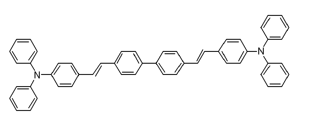
- When a dopant and a host are used together as materials for the EML, the amount of the dopant may be about 0.01 to about 15 parts by weight, based on 100 parts by weight of the host.
- The thickness of the EML may be about 100 to about 1,000 Å, for example, about 200 to about 600 Å. With such a thickness of the EML, the EML may have excellent light emitting ability without a substantial increase in driving voltage.
- When a phosphorescent dopant is also used to form the EML, a HBL may be formed between the HTL and the EML by using vacuum deposition, spin coating, casting, Langmuir-Blodgett (LB) deposition, or the like, in order to prevent diffusion of triplet excitons or holes into an ETL. When the HBL is formed using vacuum deposition or spin coating, the conditions for deposition and coating may be similar to those for the formation of the HIL, although the conditions for deposition and coating may vary according to the material that is used to form the HBL. Examples of materials for forming the HBL include an oxadiazole derivative, a triazole derivative, and a phenanthroline derivative.
- The thickness of the HBL may be about 50 to 1,000 Å, for example, about 100 to about 400 Å. With such a thickness of the HBL, the HBL may have an excellent hole blocking ability without a substantial increase in driving voltage.
- Then, an ETL may be formed on the HBL or EML by vacuum deposition, spin coating, casting, or the like. When the ETL is formed using vacuum deposition or spin coating, the deposition and coating conditions may be similar to those for formation of the HIL, although the deposition and coating conditions may vary according to a material that is used to form the ETL.
- A material for forming the ETL may include an anthracene-based compound and a quinolate-based compound that can stably transport electrons injected from an electron injecting electrode (cathode).
- The anthracene-based compound may be one represented by Formula 101 and Formula 102 below:
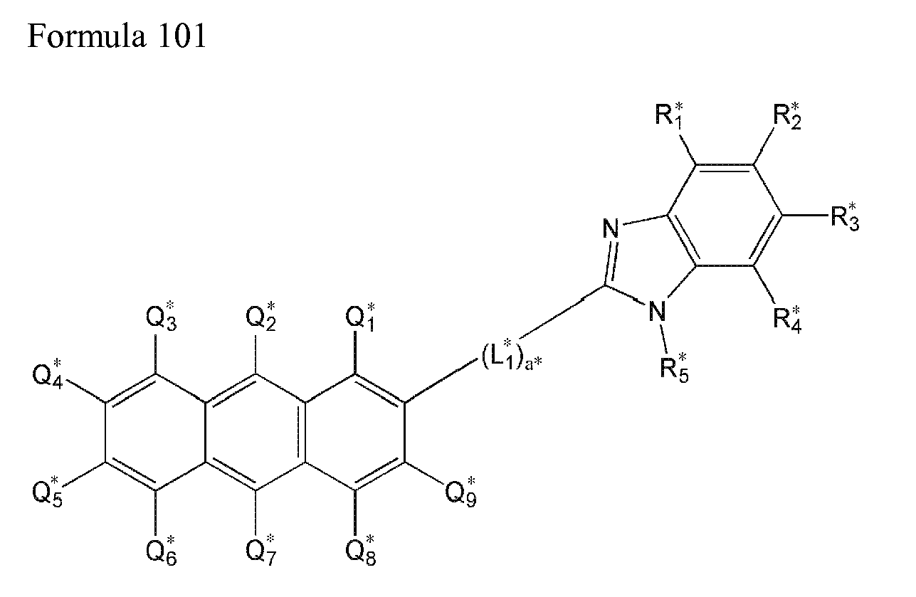
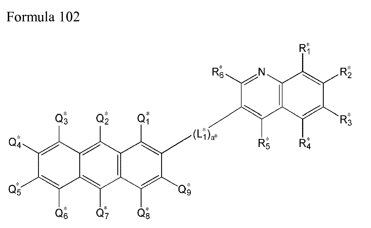
- In Formulae 101 and 102, R* 1 through R* 6 may each independently be a hydrogen atom, a halogen atom, a hydroxyl group, a cyano group, a substituted or unsubstituted C1-C30 alkyl group, a substituted or unsubstituted C1-C30 alkoxy group, a substituted or unsubstituted C1-C30 acyl group, a substituted or unsubstituted C2-C30 alkenyl group, a substituted or unsubstituted C2-C30 alkynyl group, a substituted or unsubstituted C6-C30 aryl group, or a substituted or unsubstituted C3-C30 heteroaryl group, wherein at least two adjacent groups of R*1 through R*6 may be linked together to form a saturated or unsaturated ring; L*1 may be a single bond, a substituted or unsubstituted C1-C30 alkylene group, a substituted or unsubstituted C6-C30 arylene group, or a substituted or unsubstituted C3-C30 heteroarylene group; Q*1 through Q*9 may each independently be a hydrogen atom, a substituted or unsubstituted C6-C30 aryl group, or a substituted or unsubstituted C3-C30 heteroaryl group; and a* may be an integer from 1 to 10.
- For example, the anthracene-based compound may be at least one of Formula 103 and Formula 104 below.

- The quinolate-based compound may be lithium quinolate (LiQ).
- The amounts of the anthracene-based compound and the quinolate-based compound may vary depending on the amount of holes injected from an anode to achieve optimum balance between carriers, and a ratio of the amount of the anthracene-based compound to the amount of the quinolate-based compound may be 10:5 to 10:15, for example, 10:10 taking into consideration a deposition process. As the amount of the quinolate-based compound increases, a hole blocking ability of the HBL may increase, but an electron mobility of the ETL may decrease, thereby increasing driving voltage of the OLED and reducing efficiency of the OLED. As the amount of the quinolate-based compound decreases, the ETL may exhibit dominant physical properties by the effect of the anthracene-based compound on the electron mobility of the ETL, thereby increasing driving voltage of the OLED, and reducing efficiency and lifetime of the OLED.
- The thickness of the ETL may be about 100 to about 1,000 Å, for example, about 150 to about 500 Å. With such a thickness of the ETL, the ETL may have satisfactory electron transporting ability without a substantial increase in driving voltage.
- Then, an EIL may be formed on the ETL. The EIL may be formed of a suitable material facilitating injection of electrons from a cathode.
- Examples of materials for forming the EIL include LiF, NaCl, CsF, Li2O, and BaO, which are known in the art. Deposition and coating conditions for forming the EIL may be similar to those for the formation of the HIL, although the deposition and coating conditions may vary according to a material that is used to form the EIL.
- The thickness of the EIL may be about 1 to about 100 Å, for example, about 5 to about 90 Å. With such a thickness of the EIL, the EIL may have satisfactory electron injecting ability without a substantial increase in driving voltage.
- The
second electrode 9 is disposed on theorganic layer 7. Thesecond electrode 9 may be a cathode, which is an electron injecting electrode. Thesecond electrode 9 may be formed by a metal, an alloy, or an electrically conductive compound, which have a low-work function, or a mixture thereof. In this regard, thesecond electrode 9 may be formed of lithium (Li), magnesium (Mg), aluminum (Al), aluminum (Al)-lithium (Li), calcium (Ca), magnesium (Mg)-indium (In), magnesium (Mg)-silver (Ag), or the like, and may be formed as a thin film type transmissive electrode. In addition, the transmissive electrode may be formed of indium tin oxide (ITO) or indium zinc oxide (IZO) to manufacture a top-emission type light-emitting device. - For example, the OLED may have a structure including: the first electrode; a layer including one or more cyano group-containing compounds represented by Formulae 1A through 20B, wherein the layer may further include the hole transporting compound represented by Formula 42; a HTL including the compound represented by Formula 42; an EML including a blue host (the compound represented by Formula 202) and a blue dopant (the compound represented by Formula 202); an ETL including the anthracene-based compound represented by Formula 101 and LiQ; an EIL; and a second electrode, which are sequentially stacked in this order. Thus, the OLED may emit excellent blue light due to the structure.
- The
OLED 10 may further include multiple HTLs between thefirst electrode 5 and the EML. For example, an OLED according to an embodiment may have a structure including: a substrate, a first electrode, a first HTL, a layer containing the cyano group containing compound, a second HTL, an EML, an ETL, an EIL, and a second electrode, which are sequentially stacked in this order. - In another embodiment, the OLED may include multiple layers including the cyano group-containing compound. For example, an OLED according to an embodiment may have a structure including: a substrate, a first electrode, a layer including the cyano group-containing compound, a HTL, another layer including the cyano group-containing compound, another HTL, an EML, an ETL, an EIL, and a second electrode, which are sequentially stacked in this order.
- The following Examples and Comparative Examples are provided in order to set forth particular details of one or more embodiments. The Comparative Examples are set forth to highlight certain characteristics of certain embodiments.
- A 15 Ω/cm2 (1,200 Å) ITO glass substrate (available from Coming Co.) was cut to a size of 50 mm x 50 mm x 0.7 mm, ultrasonically washed with isopropyl alcohol for 5 minutes and then with pure water for 5 minutes, and washed again with UV ozone for 30 minutes. NPB was vacuum-deposited on the ITO glass substrate to form a HTL having a thickness of 750 Å.
- 97 wt% of Compound 56 and 3 wt% of Compound 58 were deposited on the HTL to form an EML having a thickness of 200 Å.

- Alq3 was vacuum-deposited on the EML to form an ETL having a thickness of 300 Å.
- LiQ was vacuum-deposited on the ETL to form an EIL having a thickness of 5 Å and Mg and Ag were vacuum-deposited on the EIL to form a cathode having a thickness of 160 Å. Next, Alq3 was deposited on the cathode to form a protection layer having a thickness of 600 Å, thereby completing the manufacture of an OLED.
- A 15 Ω/cm2 (1,200 Å) ITO glass substrate (available from Coming Co.) was cut to a size of 50 mm x 50 mm x 0.7 mm, ultrasonically washed with isopropyl alcohol for 5 minutes and then with pure water for 5 minutes, and washed again with UV ozone for 30 minutes. A layer, instead of the HIL, was formed on the ITO glass substrate to a thickness of 100 Å, wherein the layer contained
Compound 5 above and 1 part by weight of the compound represented by Formula 20A (R109 is -F) based on 100 parts by weight of the layer.
- NPB was vacuum-deposited on the layer to form a HTL having a thickness of 750 Å. 97 wt% of Compound 56 above and 3 wt% of Compound 58 above were deposited on the HTL to form an EML having a thickness of 200 Å.
- Alq3 was vacuum-deposited on the EML to form an ETL having a thickness of 300 Å.
- LiQ was vacuum-deposited on the ETL to form an EIL having a thickness of 5 Å and Mg and Ag were vacuum-deposited on the EIL to form a cathode having a thickness of 160 Å. Next, Alq3 was deposited on the cathode to form a protection layer having a thickness of 600 Å, thereby completing the manufacture of an OLED.
- A 15 Ω/cm2 (1,200 Å) ITO glass substrate (available from Coming Co.) was cut to a size of 50 mm x 50 mm x 0.7 mm, ultrasonically washed with isopropyl alcohol for 5 minutes and then with pure water for 5 minutes, and washed again with UV ozone for 30 minutes. A layer, instead of the HIL, was formed on the ITO glass substrate to a thickness of 100 Å, wherein the layer contained
Compound 5 above and 1 part by weight of the compound represented by Formula 20A (R109 is -F) based on 100 parts by weight of the layer. - NPB was vacuum-deposited on the layer to form a HTL having a thickness of 750 Å. 97 wt% of 9,10-di(naphthalene-2-yl)anthracene (ADN) and 3 wt% of Compound 40 above were deposited on the HTL to form an EML having a thickness of 200 Å.
- Alq3 was vacuum-deposited on the EML to form an ETL having a thickness of 300 Å.
- LiQ was vacuum-deposited on the ETL to form an EIL having a thickness of 5 Å and Mg and Ag were vacuum-deposited on the EIL to form a cathode having a thickness of 160 Å. Next, Alq3 was deposited on the cathode to form a protection layer having a thickness of 600 Å, thereby completing the manufacture of an OLED.
- A 15 Ω/cm2 (1,200 Å) ITO glass substrate (available from Coming Co.) was cut to a size of 50 mm x 50 mm x 0.7 mm, ultrasonically washed with isopropyl alcohol for 5 minutes and then with pure water for 5 minutes, and washed again with UV ozone for 30 minutes. A layer, instead of the HIL, was formed on the ITO glass substrate to a thickness of 100 Å, wherein the layer contained
Compound 5 above and 1 part by weight of the compound represented by Formula 20A (R109 is -F) based on 100 parts by weight of the layer. - NPB was vacuum-deposited on the layer to form a HTL having a thickness of 750 Å. 97 wt% of 9,10-di(naphthalene-2-yl)anthracene (ADN) and 3 wt% of Compound 40 above were deposited on the HTL to form an EML having a thickness of 200 Å.
- ADN and LiQ were vacuum-deposited on the EML to form an ETL having a thickness of 300 Å.
- LiQ was vacuum-deposited on the ETL to form an EIL having a thickness of 5 Å, and Mg and Ag were vacuum-deposited on the EIL to form a cathode having a thickness of 160 Å. Next, Alq3 was deposited on the cathode to form a protection layer having a thickness of 600 Å, thereby completing the manufacture of an OLED.
- An OLED was manufactured in the same manner as in Example 1, except that 3 parts by weight of the compound represented by Formula 20A was used based on 100 parts by weight of the layer.
- Driving voltages of the OLEDs manufactured according to Comparative Examples 1 through 3 and Examples 1 and 2 were measured using a 238 High-Current Source-Measure unit (available from Keithley Instruments Inc.), and current efficiency and power efficiency thereof were measured using a PR650 Spectroscan Source Measurement Unit (available from PhotoResearch, Inc.). The results are shown in Table 1 below.
Table 1 Driving voltage (V) current efficiency (Cd/A) Color coordinate weight-calculated efficiency (Cd/Ay) Comparative Example 1 3.8 2.9 58 Comparative Example 2 3.8 3.5 76 Comparative Example 3 3.9 3.7 81 Example 1 4.1 5.4 102 Example 2 3.8 7.15 130 - Referring to Table 1, the OLEDs of Examples 1 and 2 were found to have lower driving voltages, and higher current efficiency and power efficiency, as compared to the OLEDs of Comparative Examples 1 through 3.
- As described above, an OLED according to the present invention has an excellent driving voltage characteristics, emission efficiency characteristics and power efficiency characteristics.
Claims (20)
- An organic light-emitting device (10), comprising:a substrate (1);a first electrode (5) disposed on the substrate (1);a second electrode (9);an organic layer (7) disposed between the first electrode (5) and the second electrode (9), the organic layer (7) including a hole transport layer (HTL), an emission layer (EML) and an electron transport layer (ETL); anda layer (6) disposed between the first electrode (5) and the hole transport layer (HTL), the layer (6) including at least one cyano group-containing compound.
- The organic light-emitting device as claimed in claim 1, wherein the cyano group-containing compound is one of Formulae 1 through 20:
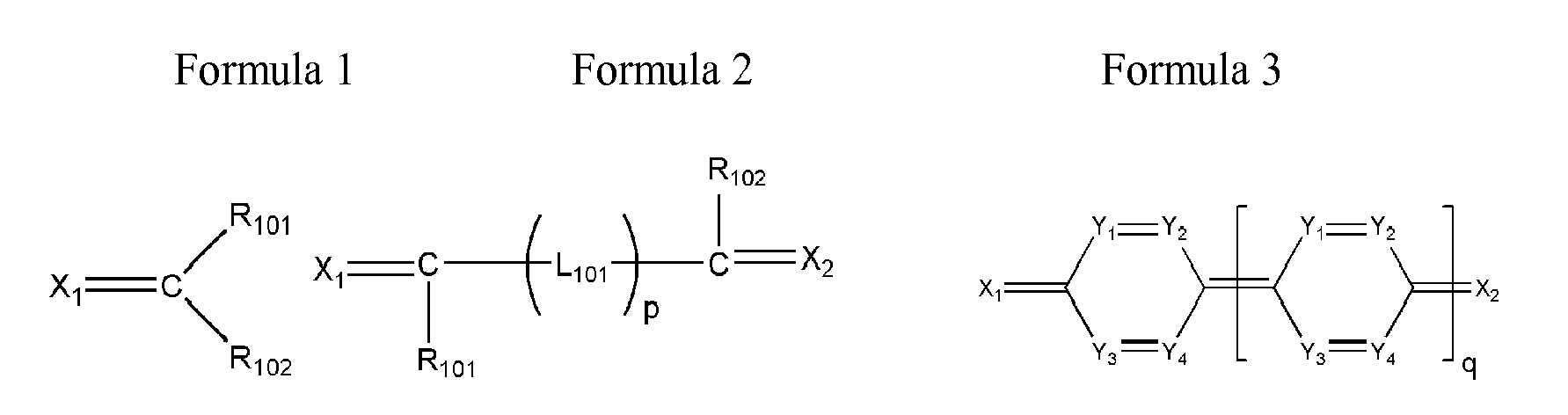


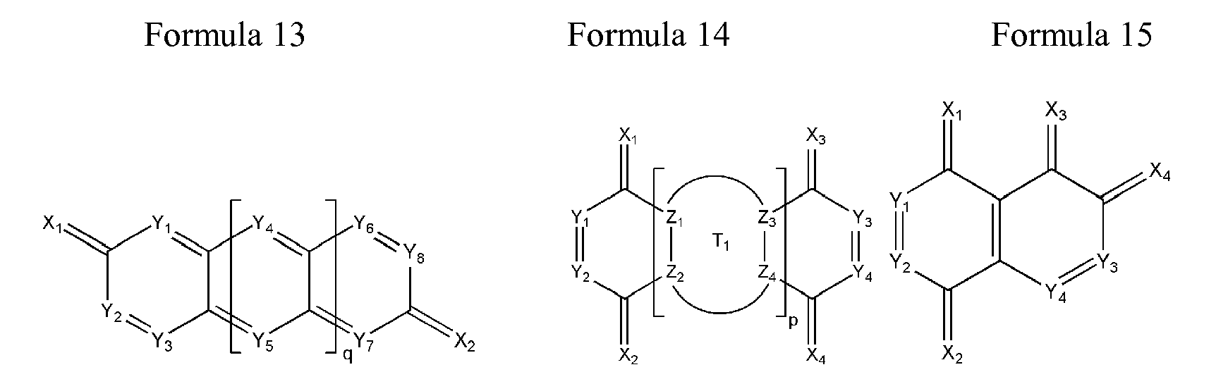


wherein, in Formulae 1 through 20,X1 through X4 are each independently compounds represented by Formulae 30A through 30D below;Y1 through Y8 are each independently N or C(R103);Z1 through Z4 are each independently C or N;A1 and A2 are each independently -O-, -S-, -N(R104), or -C(R105)(R106)-;Q101 and Q102 are each independently a C2-C10 alkylene group; a C2-C10 alkenylene group; or a substituted C2-C10 alkylene group or a substituted C2-C10 alkenylene group which have at least one substituent that is a halogen atom, a cyano group, a hydroxyl group, a C1-C10 alkyl group, or a C1-C10 alkoxy group;T1 and T2 are each independently a C5-C30 aromatic ring system; a C2-C30 heteroaromatic ring system; or a substituted C5-C30 aromatic ring system or a substituted C2-C30 heteroaromatic ring system which have at least one substituent that is a halogen atom, a cyano group, a hydroxyl group, a C1-C10 alkyl group, or a C1-C10 alkoxy group;p is an integer from 1 to 10;q is an integer from 0 to 10;R101 through R106 are each independently hydrogen; a halogen atom; a cyano group; a hydroxyl group; a C1-C10 alkyl group; a C1-C10 alkoxy group; a substituted C1-C10 alkyl group or a substituted C1-C10 alkoxy group which have at least one substituent that is a halogen atom, a cyano group, a hydroxyl group, a C5-C14 aryl group, or a C2-C14 heteroaryl group; L101 is a C5-C14 arylene group; a C5-C14 heteroarylene group; or a substituted C2-C10 alkenylene group, a substituted C5-C14 arylene group, or a substituted C5-C14 heteroarylene group which have at least one substituent that is a halogen atom, a cyano group, a hydroxyl group, a C1-C10 alkyl group, or a C1-C10 alkoxy group,
- The organic light-emitting device as claimed in claim 2, wherein X1 through X4 are each independently the compound represented by Formula 30A or the compound represented by Formula 30D.
- The organic light-emitting device as claimed in claim 2, wherein R103 is hydrogen; a halogen atom; a cyano group; a C1-C10 alkyl group; a C1-C10 alkoxy group; a substituted C1-C10 alkyl group or a substituted C1-C10 alkoxy group which have at least one substituent that is a halogen atom, a cyano group, a phenyl group, a naphthyl group, an anthryl group, a pyridinyl group, a thiophenyl group, or a benzothiophenyl group; or -N(R107)(R108), wherein R107 and R108 are each independently hydrogen, a C1-C10 alkyl group, a phenyl group, or a biphenyl group.
- The organic light-emitting device as claimed in claim 2, wherein T1 and T2 are each independently benzene; naphthalene; anthracene; thiophene; thiadiazole; oxadiazole; or a substituted benzene, a substituted naphthalene, a substituted anthracene, a substituted thiophene, a substituted thiadiazole, or a substituted oxadiazole which have at least one substituent that is a halogen atom, a cyano group, a C1-C10 alkyl group, or a C1-C10 alkoxy group.
- The organic light-emitting device as claimed in claim 2, wherein L101 is a thiophenylene group; a benzothiophenylene group; or a substituted thiophenylene group or a substituted benzothiophenylene group which have at least one substituent that is a halogen atom, a cyano group, or a C1-C10 alkyl group.
- The organic light-emitting device as claimed in claim 2, wherein the cyano group-containing compound is one of Formulae 1A through 20B:


- The organic light-emitting device as claimed in claim 1, wherein the layer (6) further includes a hole transporting compound.
- The organic light-emitting device as claimed in claim 8, wherein the hole transporting compound is one of Formula 41 or 42:

 R10 is represented by -(Ar1)n-Ar2;R16 is represented by -(Ar11)m-Ar12;Ar1, Ar11, L1, and L11 are each independently a substituted or unsubstituted C1-C30 alkylene group, a substituted or unsubstituted C2-C30 alkenylene group, a substituted or unsubstituted C5-C30 arylene group, a substituted or unsubstituted C4-C30 heteroarylene group, or -N(Q1)-;n, m, a, and b are each independently an integer from 0 to 10;R1 through R3, R11 through R15, R17, R18, R21 through R29, Ar2, Ar12, and Q1 are each independently hydrogen, a halogen atom, a hydroxyl group, a cyano group, a substituted or unsubstituted C1-C30 alkyl group, a substituted or unsubstituted C2-C30 alkenyl group, a substituted or unsubstituted C2-C30 alkynyl group, a substituted or unsubstituted C1-C30 alkoxy group, a substituted or unsubstituted C1-C30 alkylthiol group, a substituted or unsubstituted C5-C30 aryl group, a C4-C30 heteroaryl group, or -N(Q2)(Q3);Q2 and Q3 are each independently hydrogen, a halogen atom, a hydroxyl group, a cyano group, a substituted or unsubstituted C1-C30 alkyl group, a substituted or unsubstituted C2-C30 alkenyl group, a substituted or unsubstituted C2-C30 alkynyl group, a substituted or unsubstituted C1-C30 alkoxy group, a substituted or unsubstituted C1-C30 alkylthiol group, a substituted or unsubstituted C5-C30 aryl group, or a substituted or unsubstituted C4-C30 heteroaryl group; andn groups of Ar1 in -(Ar1)n- are identical to or different from each other, m groups of Ar11 in -(Ar11)m- are identical to or different from each other, a groups of L1 in -(L1)a- are identical to or different from each other, and b groups of L11 in -(L11)b- are identical to or different from each other.
 - The organic light-emitting device as claimed in claim 9, wherein Ar1 and Ar11 are each independently a C1-C10 alkylene group; a phenylene group; a naphthylene group; an anthrylene group; a fluorenylene group; a carbazolylene group; a pyrazolylene group; a pyridinylene group; a triazinylene group; -N(Q1)-; or a substituted C1-C10 alkylene group, a substituted phenylene group, a substituted naphthylene group, a substituted anthrylene group, a substituted fluorenylene group, a substituted carbazolylene group, a substituted pyrazolylene group, a substituted pyridinylene group, or a substituted triazinylene group which have at least one substituent that is a halogen atom, a cyano group, a hydroxyl group, a C1-C10 alkyl group, a C1-C10 alkoxy group, a phenyl group, a naphthyl group, or an anthryl group; and
Q1 is hydrogen; a C1-C10 alkyl group; a phenyl group; a naphthyl group; a carbazolyl group; a fluorenyl group; or a substituted C1-C10 alkyl group, a substituted C1-C10 alkoxy group, a substituted phenyl group, a substituted naphthyl group, a substituted carbazolyl group, or a substituted fluorenyl group which have at least one substituent that is a halogen atom, a cyano group, a hydroxyl group, a C1-C10 alkyl group, a C1-C10 alkoxy group, a phenyl group, a naphthyl group, or an anthryl group. - The organic light-emitting device as claimed in claim 9, wherein Ar2 and Ar12 are each independently hydrogen; a C1-C10 alkyl group; a phenyl group; a naphthyl group; a carbazolyl group; a fluorenyl group; a pyrenyl group; a substituted C1-C10 alkyl group, a substituted C1-C10 alkoxy group, a substituted phenyl group, a substituted naphthyl group, a substituted carbazolyl group, a substituted fluorenyl group, or a substituted pyrenyl group which have at least one substituent that is a halogen atom, a cyano group, a hydroxyl group, a C1-C10 alkyl group, a C1-C10 alkoxy group, a phenyl group, a naphthyl group, or an anthryl group; or -N(Q2)(Q3), wherein Q2 and Q3 are each independently hydrogen, a methyl group, an ethyl group, a phenyl group, a methylphenyl group, a biphenyl group, a naphthyl group, or a methylnaphthyl group.
- The organic light-emitting device of any of the preceding claims, wherein the amount of the cyano group-containing compound in the layer (6) is 0.1 to 20 parts by weight, based on 100 parts by weight of the layer (6).
- The organic light-emitting device of any of the preceding claims, wherein the layer (6) has a thickness of 10 Å to 2,100 Å.
- The organic light-emitting device of any of the preceding claims, wherein a distance between the layer (6) and the emission layer is 50 Å or greater.
- The organic light-emitting device of any of the preceding claims, wherein the electron transport layer (ETL) includes an anthracene-based compound and a quinolate-based compound..
- The organic light-emitting device as claimed in claim 15, wherein the anthracene-based compound is one of Formula 101 and Formula 102 below, and the quinolate-based compound is lithium quinolate (LiQ),

 R*1 through R*6 are each independently a hydrogen atom, a halogen atom, a hydroxy group, a cyano group, a substituted or unsubstituted C1-C30 alkyl group, a substituted or unsubstituted C1-C30 alkoxy group, a substituted or unsubstituted C1-C30 acyl group, a substituted or unsubstituted C2-C30 alkenyl group, a substituted or unsubstituted C2-C30 alkynyl group, a substituted or unsubstituted C6-C30 aryl group, or a substituted or unsubstituted C3-C30 heteroaryl group, wherein at least two adjacent groups of R* 1 through R*6 are linked to form a saturated or unsaturated ring;L*1 is a single bond, a substituted or unsubstituted C1-C30 alkylene group, a substituted or unsubstituted C6-C30 arylene group, or a substituted or unsubstituted C3-C30 hetero arylene group;Q*1 through Q*9 are each independently a hydrogen atom, a substituted or unsubstituted C6-C30 aryl group, or a substituted or unsubstituted C3-C30 heteroaryl group; anda* is an integer from 1 to 10.
 - The organic light-emitting device as claimed in claim 15, wherein the anthracene-based compound is one of Formula 103 and Formula 104 below, and the quinolate-based compound is lithium quinolate (LiQ),

- The organic light-emitting device of one of claims 15 through 17, wherein the amount of the anthracene-based compound is 50 to 150 parts by weight, based on 100 parts by weight of the quinolate-based compound.
- The organic light-emitting device of any of the preceding claims, wherein the emission layer (EML) includes a blue dopant and a blue host.
- The organic light-emitting device as claimed in claim 19, wherein the emission layer includes a blue dopant represented by Formula 201 below and a blue host represented by Formula 202 below,

 L21 is a substituted or unsubstituted C1-C30 alkylene group, a substituted or unsubstituted C2-C30 alkenylene group, a substituted or unsubstituted C5-C30 arylene group, or a substituted or unsubstituted C4-C30 heteroarylene group;c is an integer from 1 to 20;R31 through R34 are each independently a substituted or unsubstituted C1-C30 alkyl group, a substituted or unsubstituted C2-C30 alkenyl group, a substituted or unsubstituted C2-C30 alkynyl group, a substituted or unsubstituted C1-C30 alkoxy group, a substituted or unsubstituted C5-C30 aryl group, or a substituted or unsubstituted C4-C30 heteroaryl group.c groups of L21 in -(L21)c- are identical to or different from each other;Ar51, A52, Ar53, and Ar54 are each independently a phenylene group, a naphthylene group, an anthrylene group, or a phenyl-substituted anthrylene group,R51 through R56 are each independently a hydrogen atom, a methyl group, an ethyl group, a propyl group, a butyl group, a phenyl group, a naphthyl group, an anthryl group, a pyrenyl group, a carbazolyl group, or -N(Q2)(Q3), wherein Q2 and Q3 are each independently a methyl group, a phenyl group, a naphthyl group, or an anthryl group; andd, e, f, and g are each independently an integer from 0 to 10.
Applications Claiming Priority (1)
| Application Number | Priority Date | Filing Date | Title |
|---|---|---|---|
| KR1020100030502A KR101182446B1 (en) | 2010-04-02 | 2010-04-02 | Organic light emitting device |
Publications (3)
| Publication Number | Publication Date |
|---|---|
| EP2372807A2 true EP2372807A2 (en) | 2011-10-05 |
| EP2372807A3 EP2372807A3 (en) | 2012-02-22 |
| EP2372807B1 EP2372807B1 (en) | 2016-11-16 |
Family
ID=44146739
Family Applications (1)
| Application Number | Title | Priority Date | Filing Date |
|---|---|---|---|
| EP11160768.5A Active EP2372807B1 (en) | 2010-04-02 | 2011-04-01 | Organic light-emitting device |
Country Status (5)
| Country | Link |
|---|---|
| US (1) | US20110240969A1 (en) |
| EP (1) | EP2372807B1 (en) |
| JP (1) | JP2011222997A (en) |
| KR (1) | KR101182446B1 (en) |
| CN (1) | CN102214795B (en) |
Cited By (3)
| Publication number | Priority date | Publication date | Assignee | Title |
|---|---|---|---|---|
| EP2752907A4 (en) * | 2012-05-31 | 2015-07-29 | Lg Chemical Ltd | ORGANIC ELECTROLUMINESCENT DIODE |
| US11101432B2 (en) | 2016-01-29 | 2021-08-24 | Semiconductor Energy Laboratory Co., Ltd. | Light-emitting element, light-emitting device, electronic device, and lighting device |
| US12396075B2 (en) | 2020-12-17 | 2025-08-19 | Boe Technology Group Co., Ltd. | Blue organic electroluminescence device, display panel and display apparatus |
Families Citing this family (10)
| Publication number | Priority date | Publication date | Assignee | Title |
|---|---|---|---|---|
| JP5110198B1 (en) * | 2011-12-02 | 2012-12-26 | 東洋インキScホールディングス株式会社 | Material for organic electroluminescence device and use thereof |
| KR101952706B1 (en) * | 2012-07-24 | 2019-02-28 | 삼성디스플레이 주식회사 | Organic light-emitting device and organic light-emitting display apparatus including the same |
| KR20150119431A (en) * | 2013-02-22 | 2015-10-23 | 이데미쓰 고산 가부시키가이샤 | Anthracene derivative, material for organic electroluminescent elements, organic electroluminescent element, and electronic device |
| KR102178256B1 (en) | 2013-03-27 | 2020-11-12 | 가부시키가이샤 한도오따이 에네루기 켄큐쇼 | Light-emitting element, light-emitting device, electronic appliance, and lighting device |
| KR102269132B1 (en) | 2014-06-10 | 2021-06-25 | 삼성디스플레이 주식회사 | Antiaromatic compounds and organic light-emitting device comprising the same |
| US10084141B2 (en) | 2014-06-13 | 2018-09-25 | Samsung Display Co., Ltd. | Antiaromatic compound and organic light-emitting device including the same |
| KR102370354B1 (en) * | 2015-04-29 | 2022-03-07 | 삼성디스플레이 주식회사 | Organic light emitting device comprising the same |
| CN107188829B (en) * | 2017-05-17 | 2019-02-22 | 中节能万润股份有限公司 | A kind of OLED optoelectronic material with perfluorophenylene as the core and its application |
| KR102855273B1 (en) | 2018-07-31 | 2025-09-05 | 가부시키가이샤 한도오따이 에네루기 켄큐쇼 | Organic compounds, light-emitting elements, light-emitting devices, electronic devices, and lighting devices |
| CN113412438A (en) * | 2019-02-06 | 2021-09-17 | 株式会社半导体能源研究所 | Light-emitting device, light-emitting apparatus, electronic apparatus, display apparatus, and lighting apparatus |
Family Cites Families (18)
| Publication number | Priority date | Publication date | Assignee | Title |
|---|---|---|---|---|
| KR100691543B1 (en) * | 2002-01-18 | 2007-03-09 | 주식회사 엘지화학 | New material for electron transport and organic light emitting device using the same |
| JP2004063363A (en) * | 2002-07-31 | 2004-02-26 | Semiconductor Energy Lab Co Ltd | Electroluminescent device material and electroluminescent device using the same |
| JP2004091334A (en) * | 2002-08-29 | 2004-03-25 | Mitsubishi Chemicals Corp | 2,6-Arylaminoanthracene-based compound, charge transport material, and organic electroluminescent device |
| DE10357044A1 (en) * | 2003-12-04 | 2005-07-14 | Novaled Gmbh | Process for doping organic semiconductors with quinonediimine derivatives |
| US20050147844A1 (en) * | 2004-01-05 | 2005-07-07 | Eastman Kodak Company | White oled devices with color filter arrays |
| KR100573137B1 (en) * | 2004-04-02 | 2006-04-24 | 삼성에스디아이 주식회사 | Fluorene compound and organic electroluminescent device using same |
| KR100669790B1 (en) * | 2004-11-27 | 2007-01-16 | 삼성에스디아이 주식회사 | Organic electroluminescent element |
| US20060159953A1 (en) * | 2005-01-20 | 2006-07-20 | Labeltek Inc. | Diarylamino substituted arylvinyl naphthalene compounds and a blue-light electroluminescent device having the compounds |
| DE102005010979A1 (en) * | 2005-03-04 | 2006-09-21 | Technische Universität Dresden | Photoactive component with organic layers |
| US20060286405A1 (en) * | 2005-06-17 | 2006-12-21 | Eastman Kodak Company | Organic element for low voltage electroluminescent devices |
| KR100672535B1 (en) * | 2005-07-25 | 2007-01-24 | 엘지전자 주식회사 | Organic electroluminescence device and method for fabricating the same |
| US7919195B2 (en) * | 2007-01-11 | 2011-04-05 | Chimei Innolux Corporation | System for displaying images |
| US20080176099A1 (en) * | 2007-01-18 | 2008-07-24 | Hatwar Tukaram K | White oled device with improved functions |
| US20100133996A1 (en) * | 2007-05-09 | 2010-06-03 | Dongjin Semichem Co., Ltd | Novel anthracene typed compound and the organic electroluminescence display device using the same |
| US8367219B2 (en) * | 2007-10-30 | 2013-02-05 | Samsung Electronics Co., Ltd. | Anthracene-based compound and organic light emitting device employing the same |
| KR20090098585A (en) * | 2008-03-14 | 2009-09-17 | (주)그라쎌 | Organic electroluminescent device employing organic light emitting compound as light emitting material |
| JP2009289596A (en) * | 2008-05-29 | 2009-12-10 | Seiko Epson Corp | Method of manufacturing light-emitting device, and light-emitting device, display device, and electronic equipment |
| KR100924144B1 (en) * | 2008-06-05 | 2009-10-28 | 삼성모바일디스플레이주식회사 | Organic electroluminescent device and manufacturing method thereof |
-
2010
- 2010-04-02 KR KR1020100030502A patent/KR101182446B1/en active Active
-
2011
- 2011-04-01 EP EP11160768.5A patent/EP2372807B1/en active Active
- 2011-04-01 US US13/064,583 patent/US20110240969A1/en not_active Abandoned
- 2011-04-02 CN CN201110085826.9A patent/CN102214795B/en active Active
- 2011-04-04 JP JP2011082867A patent/JP2011222997A/en active Pending
Non-Patent Citations (1)
| Title |
|---|
| None |
Cited By (5)
| Publication number | Priority date | Publication date | Assignee | Title |
|---|---|---|---|---|
| EP2752907A4 (en) * | 2012-05-31 | 2015-07-29 | Lg Chemical Ltd | ORGANIC ELECTROLUMINESCENT DIODE |
| US9831457B2 (en) | 2012-05-31 | 2017-11-28 | Lg Display Co., Ltd. | Organic light emitting diode |
| US11101432B2 (en) | 2016-01-29 | 2021-08-24 | Semiconductor Energy Laboratory Co., Ltd. | Light-emitting element, light-emitting device, electronic device, and lighting device |
| US12089491B2 (en) | 2016-01-29 | 2024-09-10 | Semiconductor Energy Laboratory Co., Ltd. | Light-emitting element, light-emitting device, electronic device, and lighting device |
| US12396075B2 (en) | 2020-12-17 | 2025-08-19 | Boe Technology Group Co., Ltd. | Blue organic electroluminescence device, display panel and display apparatus |
Also Published As
| Publication number | Publication date |
|---|---|
| KR20110111103A (en) | 2011-10-10 |
| KR101182446B1 (en) | 2012-09-12 |
| JP2011222997A (en) | 2011-11-04 |
| CN102214795B (en) | 2015-07-22 |
| US20110240969A1 (en) | 2011-10-06 |
| EP2372807B1 (en) | 2016-11-16 |
| EP2372807A3 (en) | 2012-02-22 |
| CN102214795A (en) | 2011-10-12 |
Similar Documents
| Publication | Publication Date | Title |
|---|---|---|
| EP2372807B1 (en) | Organic light-emitting device | |
| KR101097315B1 (en) | Organic light emitting device | |
| KR101097316B1 (en) | organic light emitting device | |
| JP6192699B2 (en) | ORGANIC LIGHT EMITTING DEVICE AND MANUFACTURING METHOD THEREOF | |
| US9379334B2 (en) | Organic light-emitting device | |
| JP5420825B2 (en) | Organic light emitting device | |
| CN103904227B (en) | Organic light emitting diode | |
| KR102081281B1 (en) | Organic light emitting device | |
| US9786847B2 (en) | Compound for organic photoelectric device, and organic photoelectric device and image sensor including the same | |
| WO2022263531A1 (en) | Active-matrix oled display | |
| CN118742177A (en) | An organic electroluminescent device and a display device containing the same | |
| EP3435437A1 (en) | Organic light-emitting element | |
| EP4356449A1 (en) | Sheet resistance component | |
| KR20120001706A (en) | Organic light emitting device |
Legal Events
| Date | Code | Title | Description |
|---|---|---|---|
| PUAI | Public reference made under article 153(3) epc to a published international application that has entered the european phase |
Free format text: ORIGINAL CODE: 0009012 |
|
| AK | Designated contracting states |
Kind code of ref document: A2 Designated state(s): AL AT BE BG CH CY CZ DE DK EE ES FI FR GB GR HR HU IE IS IT LI LT LU LV MC MK MT NL NO PL PT RO RS SE SI SK SM TR |
|
| AX | Request for extension of the european patent |
Extension state: BA ME |
|
| PUAL | Search report despatched |
Free format text: ORIGINAL CODE: 0009013 |
|
| AK | Designated contracting states |
Kind code of ref document: A3 Designated state(s): AL AT BE BG CH CY CZ DE DK EE ES FI FR GB GR HR HU IE IS IT LI LT LU LV MC MK MT NL NO PL PT RO RS SE SI SK SM TR |
|
| AX | Request for extension of the european patent |
Extension state: BA ME |
|
| RIC1 | Information provided on ipc code assigned before grant |
Ipc: H01L 51/54 20060101AFI20120117BHEP |
|
| 17P | Request for examination filed |
Effective date: 20120622 |
|
| RAP1 | Party data changed (applicant data changed or rights of an application transferred) |
Owner name: SAMSUNG DISPLAY CO., LTD. |
|
| 17Q | First examination report despatched |
Effective date: 20150626 |
|
| RAP1 | Party data changed (applicant data changed or rights of an application transferred) |
Owner name: SAMSUNG DISPLAY CO., LTD. |
|
| RIC1 | Information provided on ipc code assigned before grant |
Ipc: H01L 51/54 20060101AFI20160705BHEP |
|
| GRAP | Despatch of communication of intention to grant a patent |
Free format text: ORIGINAL CODE: EPIDOSNIGR1 |
|
| INTG | Intention to grant announced |
Effective date: 20160819 |
|
| GRAS | Grant fee paid |
Free format text: ORIGINAL CODE: EPIDOSNIGR3 |
|
| GRAA | (expected) grant |
Free format text: ORIGINAL CODE: 0009210 |
|
| AK | Designated contracting states |
Kind code of ref document: B1 Designated state(s): AL AT BE BG CH CY CZ DE DK EE ES FI FR GB GR HR HU IE IS IT LI LT LU LV MC MK MT NL NO PL PT RO RS SE SI SK SM TR |
|
| REG | Reference to a national code |
Ref country code: GB Ref legal event code: FG4D |
|
| REG | Reference to a national code |
Ref country code: CH Ref legal event code: EP |
|
| REG | Reference to a national code |
Ref country code: IE Ref legal event code: FG4D |
|
| REG | Reference to a national code |
Ref country code: AT Ref legal event code: REF Ref document number: 846666 Country of ref document: AT Kind code of ref document: T Effective date: 20161215 |
|
| REG | Reference to a national code |
Ref country code: DE Ref legal event code: R096 Ref document number: 602011032372 Country of ref document: DE |
|
| REG | Reference to a national code |
Ref country code: NL Ref legal event code: FP |
|
| PG25 | Lapsed in a contracting state [announced via postgrant information from national office to epo] |
Ref country code: LV Free format text: LAPSE BECAUSE OF FAILURE TO SUBMIT A TRANSLATION OF THE DESCRIPTION OR TO PAY THE FEE WITHIN THE PRESCRIBED TIME-LIMIT Effective date: 20161116 |
|
| REG | Reference to a national code |
Ref country code: LT Ref legal event code: MG4D |
|
| REG | Reference to a national code |
Ref country code: AT Ref legal event code: MK05 Ref document number: 846666 Country of ref document: AT Kind code of ref document: T Effective date: 20161116 |
|
| REG | Reference to a national code |
Ref country code: FR Ref legal event code: PLFP Year of fee payment: 7 |
|
| PG25 | Lapsed in a contracting state [announced via postgrant information from national office to epo] |
Ref country code: NO Free format text: LAPSE BECAUSE OF FAILURE TO SUBMIT A TRANSLATION OF THE DESCRIPTION OR TO PAY THE FEE WITHIN THE PRESCRIBED TIME-LIMIT Effective date: 20170216 Ref country code: LT Free format text: LAPSE BECAUSE OF FAILURE TO SUBMIT A TRANSLATION OF THE DESCRIPTION OR TO PAY THE FEE WITHIN THE PRESCRIBED TIME-LIMIT Effective date: 20161116 Ref country code: SE Free format text: LAPSE BECAUSE OF FAILURE TO SUBMIT A TRANSLATION OF THE DESCRIPTION OR TO PAY THE FEE WITHIN THE PRESCRIBED TIME-LIMIT Effective date: 20161116 Ref country code: GR Free format text: LAPSE BECAUSE OF FAILURE TO SUBMIT A TRANSLATION OF THE DESCRIPTION OR TO PAY THE FEE WITHIN THE PRESCRIBED TIME-LIMIT Effective date: 20170217 |
|
| PG25 | Lapsed in a contracting state [announced via postgrant information from national office to epo] |
Ref country code: HR Free format text: LAPSE BECAUSE OF FAILURE TO SUBMIT A TRANSLATION OF THE DESCRIPTION OR TO PAY THE FEE WITHIN THE PRESCRIBED TIME-LIMIT Effective date: 20161116 Ref country code: AT Free format text: LAPSE BECAUSE OF FAILURE TO SUBMIT A TRANSLATION OF THE DESCRIPTION OR TO PAY THE FEE WITHIN THE PRESCRIBED TIME-LIMIT Effective date: 20161116 Ref country code: ES Free format text: LAPSE BECAUSE OF FAILURE TO SUBMIT A TRANSLATION OF THE DESCRIPTION OR TO PAY THE FEE WITHIN THE PRESCRIBED TIME-LIMIT Effective date: 20161116 Ref country code: PL Free format text: LAPSE BECAUSE OF FAILURE TO SUBMIT A TRANSLATION OF THE DESCRIPTION OR TO PAY THE FEE WITHIN THE PRESCRIBED TIME-LIMIT Effective date: 20161116 Ref country code: PT Free format text: LAPSE BECAUSE OF FAILURE TO SUBMIT A TRANSLATION OF THE DESCRIPTION OR TO PAY THE FEE WITHIN THE PRESCRIBED TIME-LIMIT Effective date: 20170316 Ref country code: RS Free format text: LAPSE BECAUSE OF FAILURE TO SUBMIT A TRANSLATION OF THE DESCRIPTION OR TO PAY THE FEE WITHIN THE PRESCRIBED TIME-LIMIT Effective date: 20161116 Ref country code: FI Free format text: LAPSE BECAUSE OF FAILURE TO SUBMIT A TRANSLATION OF THE DESCRIPTION OR TO PAY THE FEE WITHIN THE PRESCRIBED TIME-LIMIT Effective date: 20161116 |
|
| PG25 | Lapsed in a contracting state [announced via postgrant information from national office to epo] |
Ref country code: DK Free format text: LAPSE BECAUSE OF FAILURE TO SUBMIT A TRANSLATION OF THE DESCRIPTION OR TO PAY THE FEE WITHIN THE PRESCRIBED TIME-LIMIT Effective date: 20161116 Ref country code: SK Free format text: LAPSE BECAUSE OF FAILURE TO SUBMIT A TRANSLATION OF THE DESCRIPTION OR TO PAY THE FEE WITHIN THE PRESCRIBED TIME-LIMIT Effective date: 20161116 Ref country code: EE Free format text: LAPSE BECAUSE OF FAILURE TO SUBMIT A TRANSLATION OF THE DESCRIPTION OR TO PAY THE FEE WITHIN THE PRESCRIBED TIME-LIMIT Effective date: 20161116 Ref country code: CZ Free format text: LAPSE BECAUSE OF FAILURE TO SUBMIT A TRANSLATION OF THE DESCRIPTION OR TO PAY THE FEE WITHIN THE PRESCRIBED TIME-LIMIT Effective date: 20161116 Ref country code: RO Free format text: LAPSE BECAUSE OF FAILURE TO SUBMIT A TRANSLATION OF THE DESCRIPTION OR TO PAY THE FEE WITHIN THE PRESCRIBED TIME-LIMIT Effective date: 20161116 |
|
| REG | Reference to a national code |
Ref country code: DE Ref legal event code: R097 Ref document number: 602011032372 Country of ref document: DE |
|
| PG25 | Lapsed in a contracting state [announced via postgrant information from national office to epo] |
Ref country code: IT Free format text: LAPSE BECAUSE OF FAILURE TO SUBMIT A TRANSLATION OF THE DESCRIPTION OR TO PAY THE FEE WITHIN THE PRESCRIBED TIME-LIMIT Effective date: 20161116 Ref country code: BE Free format text: LAPSE BECAUSE OF FAILURE TO SUBMIT A TRANSLATION OF THE DESCRIPTION OR TO PAY THE FEE WITHIN THE PRESCRIBED TIME-LIMIT Effective date: 20161116 Ref country code: SM Free format text: LAPSE BECAUSE OF FAILURE TO SUBMIT A TRANSLATION OF THE DESCRIPTION OR TO PAY THE FEE WITHIN THE PRESCRIBED TIME-LIMIT Effective date: 20161116 Ref country code: BG Free format text: LAPSE BECAUSE OF FAILURE TO SUBMIT A TRANSLATION OF THE DESCRIPTION OR TO PAY THE FEE WITHIN THE PRESCRIBED TIME-LIMIT Effective date: 20170216 |
|
| PLBE | No opposition filed within time limit |
Free format text: ORIGINAL CODE: 0009261 |
|
| STAA | Information on the status of an ep patent application or granted ep patent |
Free format text: STATUS: NO OPPOSITION FILED WITHIN TIME LIMIT |
|
| 26N | No opposition filed |
Effective date: 20170817 |
|
| PG25 | Lapsed in a contracting state [announced via postgrant information from national office to epo] |
Ref country code: SI Free format text: LAPSE BECAUSE OF FAILURE TO SUBMIT A TRANSLATION OF THE DESCRIPTION OR TO PAY THE FEE WITHIN THE PRESCRIBED TIME-LIMIT Effective date: 20161116 |
|
| REG | Reference to a national code |
Ref country code: CH Ref legal event code: PL |
|
| REG | Reference to a national code |
Ref country code: IE Ref legal event code: MM4A |
|
| PG25 | Lapsed in a contracting state [announced via postgrant information from national office to epo] |
Ref country code: MC Free format text: LAPSE BECAUSE OF FAILURE TO SUBMIT A TRANSLATION OF THE DESCRIPTION OR TO PAY THE FEE WITHIN THE PRESCRIBED TIME-LIMIT Effective date: 20161116 |
|
| PG25 | Lapsed in a contracting state [announced via postgrant information from national office to epo] |
Ref country code: CH Free format text: LAPSE BECAUSE OF NON-PAYMENT OF DUE FEES Effective date: 20170430 Ref country code: LU Free format text: LAPSE BECAUSE OF NON-PAYMENT OF DUE FEES Effective date: 20170401 Ref country code: LI Free format text: LAPSE BECAUSE OF NON-PAYMENT OF DUE FEES Effective date: 20170430 |
|
| REG | Reference to a national code |
Ref country code: FR Ref legal event code: PLFP Year of fee payment: 8 |
|
| PG25 | Lapsed in a contracting state [announced via postgrant information from national office to epo] |
Ref country code: IE Free format text: LAPSE BECAUSE OF NON-PAYMENT OF DUE FEES Effective date: 20170401 |
|
| PG25 | Lapsed in a contracting state [announced via postgrant information from national office to epo] |
Ref country code: MT Free format text: LAPSE BECAUSE OF NON-PAYMENT OF DUE FEES Effective date: 20170401 |
|
| PG25 | Lapsed in a contracting state [announced via postgrant information from national office to epo] |
Ref country code: HU Free format text: LAPSE BECAUSE OF FAILURE TO SUBMIT A TRANSLATION OF THE DESCRIPTION OR TO PAY THE FEE WITHIN THE PRESCRIBED TIME-LIMIT; INVALID AB INITIO Effective date: 20110401 |
|
| PG25 | Lapsed in a contracting state [announced via postgrant information from national office to epo] |
Ref country code: CY Free format text: LAPSE BECAUSE OF NON-PAYMENT OF DUE FEES Effective date: 20161116 |
|
| PG25 | Lapsed in a contracting state [announced via postgrant information from national office to epo] |
Ref country code: MK Free format text: LAPSE BECAUSE OF FAILURE TO SUBMIT A TRANSLATION OF THE DESCRIPTION OR TO PAY THE FEE WITHIN THE PRESCRIBED TIME-LIMIT Effective date: 20161116 |
|
| PG25 | Lapsed in a contracting state [announced via postgrant information from national office to epo] |
Ref country code: TR Free format text: LAPSE BECAUSE OF FAILURE TO SUBMIT A TRANSLATION OF THE DESCRIPTION OR TO PAY THE FEE WITHIN THE PRESCRIBED TIME-LIMIT Effective date: 20161116 |
|
| PG25 | Lapsed in a contracting state [announced via postgrant information from national office to epo] |
Ref country code: AL Free format text: LAPSE BECAUSE OF FAILURE TO SUBMIT A TRANSLATION OF THE DESCRIPTION OR TO PAY THE FEE WITHIN THE PRESCRIBED TIME-LIMIT Effective date: 20161116 Ref country code: IS Free format text: LAPSE BECAUSE OF FAILURE TO SUBMIT A TRANSLATION OF THE DESCRIPTION OR TO PAY THE FEE WITHIN THE PRESCRIBED TIME-LIMIT Effective date: 20170316 |
|
| REG | Reference to a national code |
Ref country code: DE Ref legal event code: R079 Ref document number: 602011032372 Country of ref document: DE Free format text: PREVIOUS MAIN CLASS: H01L0051540000 Ipc: H10K0085000000 |
|
| P01 | Opt-out of the competence of the unified patent court (upc) registered |
Effective date: 20230515 |
|
| PGFP | Annual fee paid to national office [announced via postgrant information from national office to epo] |
Ref country code: DE Payment date: 20250320 Year of fee payment: 15 |
|
| PGFP | Annual fee paid to national office [announced via postgrant information from national office to epo] |
Ref country code: GB Payment date: 20260324 Year of fee payment: 16 |
|
| PGFP | Annual fee paid to national office [announced via postgrant information from national office to epo] |
Ref country code: NL Payment date: 20260324 Year of fee payment: 16 |
|
| PGFP | Annual fee paid to national office [announced via postgrant information from national office to epo] |
Ref country code: FR Payment date: 20260323 Year of fee payment: 16 |