EP2372754A1 - Spacer formation in the fabrication of planar bipolar transistors - Google Patents
Spacer formation in the fabrication of planar bipolar transistors Download PDFInfo
- Publication number
- EP2372754A1 EP2372754A1 EP10250714A EP10250714A EP2372754A1 EP 2372754 A1 EP2372754 A1 EP 2372754A1 EP 10250714 A EP10250714 A EP 10250714A EP 10250714 A EP10250714 A EP 10250714A EP 2372754 A1 EP2372754 A1 EP 2372754A1
- Authority
- EP
- European Patent Office
- Prior art keywords
- spacer
- layer
- base
- forming
- width
- Prior art date
- Legal status (The legal status is an assumption and is not a legal conclusion. Google has not performed a legal analysis and makes no representation as to the accuracy of the status listed.)
- Granted
Links
Images


Classifications
-
- H—ELECTRICITY
- H10—SEMICONDUCTOR DEVICES; ELECTRIC SOLID-STATE DEVICES NOT OTHERWISE PROVIDED FOR
- H10D—INORGANIC ELECTRIC SEMICONDUCTOR DEVICES
- H10D10/00—Bipolar junction transistors [BJT]
- H10D10/01—Manufacture or treatment
- H10D10/021—Manufacture or treatment of heterojunction BJTs [HBT]
-
- H—ELECTRICITY
- H10—SEMICONDUCTOR DEVICES; ELECTRIC SOLID-STATE DEVICES NOT OTHERWISE PROVIDED FOR
- H10D—INORGANIC ELECTRIC SEMICONDUCTOR DEVICES
- H10D62/00—Semiconductor bodies, or regions thereof, of devices having potential barriers
- H10D62/10—Shapes, relative sizes or dispositions of the regions of the semiconductor bodies; Shapes of the semiconductor bodies
- H10D62/13—Semiconductor regions connected to electrodes carrying current to be rectified, amplified or switched, e.g. source or drain regions
- H10D62/133—Emitter regions of BJTs
- H10D62/136—Emitter regions of BJTs of heterojunction BJTs
Definitions
- the present invention relates to planar bipolar transistors and in particular, though not exclusively, to the fabrication of heterojunction bipolar transistors such as those using a low-complexity SiGe:C architecture.
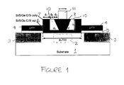
- FIG. 1 A schematic diagram of a conventional planar low-complexity heterojunction bipolar transistor (HBT) is shown in figure 1 .
- a semiconductor substrate 1 serves as a collector region 2 surrounded by a shallow trench isolation (STI) region 3.
- a polysilicon gate 4 provides an electrical connection to a base epitaxial layer 6 via a polysilicon base stack 7.
- the base stack 7 is the vertical portion of the base semiconductor region.
- the polysilicon gate layer 4 is separated from the STI region and substrate 1 by a gate oxide layer 5.
- An emitter 8 is in contact with the base at an emitter window 9 having an emitter window width W E .
- the emitter 8 is otherwise electrically isolated from the base epitaxial layer 6 and the polysilicon base stack 7 by spacers 10, formed in a suitable electrically insulating material such as silicon oxide.
- the emitter 8 has an electrical contact 11 formed on its surface. Electrical contacts for the base and collector are not shown on this schematic diagram but can be made to the polysilicon gate 4 and to the collector region 2 via the substrate 1 beyond the shallow trench isolation regions 3.
- the spacers 10 have a number of important design constraints.
- the spacer width d 2 at the top of the spacer 10 must not be too small or it will be bridged when a silicide layer is subsequently formed on the top surfaces of the polysilicon base stack 7 and the emitter 8. The formation of silicide on these surfaces is required to create good electrical contacts to the emitter and base.
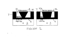
- increasing the width d 2 of the spacer 10 at the top results in an increase in the width d 5 of the spacer 10 at the bottom which in turn leads to a reduction in the emitter window size W E , an increase in the base link resistance (i.e. a longer base current path beneath the spacer 10) and a higher extrinsic base-collector capacitance, i.e.
- the spacers can be formed in an "L" shape. This is shown schematically in figure 3 where the structure of the transistor is shown using L-shaped spacers 20. These L-shaped spacers 20 can be formed using a process as shown with reference to figure 4 .
- a polysilicon base stack 7 has a first thin oxide layer 41, thin nitride layer 42 and second thin oxide layer 43 formed thereon.
- a polysilicon spacer layer 44 is deposited over that.
- An anisotropic etch of the polysilicon layer 44 creates a polysilicon spacer 45 as shown in figure 4b, consuming a bit of the second oxide layer 43 underneath.
- the nitride layer 42 is etched using the first oxide layer 41 as a hard mask.
- the polysilicon spacer 45 is also consumed leaving a thin L-shaped spacer 20 which will subsequently serve to separate the base 7 and the emitter 8 except in the emitter window 9.
- SEM scanning electron micrograph
- the present invention provides method of forming a bipolar transistor, comprising the steps of:
- the step of forming a base of the transistor may include: forming a first base layer on the substrate; forming a planarization layer on the first base layer; defining a base window through the planarization layer and the first base layer to expose the collector region, including etching the planarization layer to a greater lateral extent than the first base layer on which it is formed; depositing a base epitaxial layer on the exposed collector region and a base stack on sidewalls of the base window; the method further including the steps of: forming the spacer by forming an electrically insulating layer in the base window and etching the insulating layer so as to leave a residual portion thereof that covers the portion of the base stack that forms the sidewalls of the base window, wherein the greater lateral extent of the etch of the planarization layer results in a widening of the spacer or a sloping outward of the spacer at least part way up the spacer.
- the emitter region may be formed in the base window by depositing a semiconductor material over the first base layer and the spacer. Planarizing the structure may be by removing all layers down to a depth part way through the planarization layer. Planarizing the structure may comprise removing all layers down to a depth corresponding to a widest part of the spacer.
- a silicide layer may be formed on the base stack and the emitter region on either side of the spacer, the silicide layer being discontinuous over the top surface of the spacer.
- the base of the transistor may be formed by forming a cap layer on the planarization layer and defining the base window through said cap layer as well as said planarization layer and said base silicon layer, wherein the etching of the planarization layer is performed to a greater lateral extent than the etching of the cap layer so as to undercut the cap layer and form a recessed portion of the base window sidewall prior to forming the base stack thereon.
- the spacer may be formed by forming the electrically insulating layer as a three layer structure comprising a first silicon oxide layer, a silicon nitride layer and a second silicon oxide layer and wherein the etching of said layers to leave said residual portion comprises etching the second silicon layer to end point on the nitride layer, then removing the exposed nitride layer.
- the spacer may be formed so as to have one of a gamma-shaped or inverted L-shaped structure, or an oblique shape.
- the present invention provides a bipolar transistor structure having a collector formed in a substrate and a base and an emitter formed over the substrate, the base having a base stack region being laterally separated from the emitter on the substrate by an electrically insulating spacer, in which the insulating spacer has a width dimension at its top end at least as large as the width dimension at its bottom end.
- the spacer may have a width dimension at its top end larger than the width dimension at its bottom end.
- the spacer may be formed as a r-shaped or inverted L-shaped structure.
- the spacer may be formed as an oblique spacer in which the spacer has a generally uniform width or a width which increases slightly towards the top of the spacer, and where the top surface that has a width substantially the same as, or greater than, the width of the bottom surface, is displaced laterally outwardly from the bottom surface.
- the oblique spacer may have a curved profile, such that it presents a convex surface to the emitter and a concave surface to the base stack region.
- the spacer may be formed from a silicon oxide or from a silicon oxide and silicon nitride layered structure.
- the inventors have recognised that it would be advantageous to provide a spacer which separates parts of the base and emitter of the transistor in which the spacer is at least as wide at the top of the spacer as it is at the base of the spacer. More preferably, it would be advantageous to provide such a spacer which is wider at the top of the spacer than it is at the bottom of the spacer. A number of process techniques for the formation of such a spacer are now described.
- collector or “collector region”, “base region” and “emitter region” are used for convenience to respectively define (i) a first region in the semiconductor substrate that provides a first dopant level and dopant type, (ii) a second region of semiconductor disposed on the substrate and having a second dopant level and second dopant type to form a junction with the first region, and (iii) a third region of semiconductor disposed on the second region and having a third dopant level and third dopant type.
- the first and third dopant types could be the same.
- the first, second and third dopant types could be n, p, n respectively, or p, n, p respectively. It will be understood that the devices described here could be inverted so that an emitter region is formed in the substrate and a collector region formed over the substrate. The labels are to be construed accordingly.
- a first process for creating a r-shaped (gamma-shaped) spacer is described with reference to figures 6 to 11 .
- the process is shown with schematic cross-sections.
- an L-shaped spacer process as discussed in connection with figure 4 is illustrated on the left hand side of the respective figure and the modified process for producing a gamma-shaped spacer is illustrated on the right hand side of the figure, for easy comparison.
- a collector region 52 and shallow trench isolation regions 53 in conventional manner.
- a polysilicon gate layer 54 is deposited onto the substrate, followed by a silicon nitride planarization (CMP stopping) layer 55 and a polysilicon cap layer 56.
- CMP stopping silicon nitride planarization
- a photolithography stage follows to define a base window opening in photoresist (not shown) over the polysilicon cap layer 56.
- the base window 60 is then formed by etching through the polysilicon cap layer 56, the nitride layer 55 and the polysilicon gate layer 54. This is preferably performed using a single anisotropic etch, e.g. dry etch process.
- This dry etch is followed by a separate lateral etch of the nitride layer 55 to undercut the polysilicon cap layer to provide a somewhat re-entrant or recessed profile of the walls of the base window 60, as shown in figure 6 .
- This nitride etch is preferably a wet etch process, e.g. using H 3 PO 4 .
- the recess 61 in the nitride layer 55 is shown greatly exaggerated for clarity, as will become apparent later.
- the polysilicon cap layer 56 does not form part of an L-shaped spacer production process on the left hand side of the figure.
- the photoresist layer may be removed after the first (dry) etch process, or after the second (wet) etch process.
- etch strategies may be possible to obtain the required profile of base window, for example by a separate first etch through the polysilicon cap layer 56 followed by a second etch through the nitride layer 55 and a third etch through the polysilicon gate layer 54.
- a base stack 57 and epitaxial base layer 58 of Si/SiGe:C/Si is then formed over the etched base window profile resulting in the structure shown in figure 6 .
- a spacer 63 is formed by deposition of a suitable spacer material which fills the base window 60 and is then etched back using a process similar to that shown in figure 2 .
- the spacer formation process first forms a first thin layer of silicon oxide 41, followed by a layer of silicon nitride 42, followed by a second thin layer of silicon oxide 43 followed by a polysilicon spacer material which is then processed similar to that described for figure 2 .
- the spacer formation process first forms a first thin layer of silicon oxide 41, followed by a layer of silicon nitride 42, followed by a second much thicker layer of silicon oxide 43.
- a dielectric layer is preferred for the spacers, e.g. silicon oxide or silicon nitride.
- the layer of silicon oxide could be formed using a known TEOS deposition process.
- An anisotropic etch of the second oxide layer 43 to an endpoint of exposure of the nitride layer 42 leaves a wedge-shaped oxide spacer 63 as shown in figure 7 .
- the spacer could be formed using various processes, including use of only oxide layers, using the oxide and nitride layers as shown, or using a polysilicon-based spacer as shown in figure 2 .
- the use of an oxide-nitride-oxide sandwich is preferred as it allows for triggering an etch endpoint on exposure of the nitride layer.
- the spacer may be formed from any suitable electrically insulating material such as a dielectric material or combination of insulating layers which facilitate generally conformal coverage of the recessed or stepped base window profile and a subsequent etch that stops on the epitaxial base layer 58 in the emitter window 9 while leaving some coverage on the sidewalls of the base stack.
- the width of the lower part of the spacer is a function of the deposited thickness of the oxide (or other spacer material), the height of the step (sum of deposited polysilicon gate layer 54 + silicon nitride CMP stopping layer 55 + polysilicon cap layer 56) and the total etch time.
- the uncovered thin nitride layer 42 is removed using a suitable wet etch, with the remaining second oxide layer 43 acting as a hard mask.
- the remaining exposed first thin oxide layer 41 on the base stack layer 57 and epitaxial base layer 58 is removed and then a polysilicon emitter layer 59 is deposited, resulting in the structure shown in figure 8 .
- a planarization process follows that aims to stop halfway through the nitride planarization layer 55, as shown in figure 9 .
- all layers are removed in a planar fashion, e.g. using a chemical and/or mechanical removal process as known in the art, down to a level part way through the planarization layer 55.
- the nitride planarization layer 55 thickness (t nit ) can be tuned to meet the planarization within-wafer-uniformity requirements: a thicker nitride layer 55 creates a larger thickness of oxide (t ox ) in the recessed portion 61 of the spacer, as shown in figure 8 .
- the planarization process stops approximately at a midpoint of the planarization layer. More preferably, the planarization process stops approximately at the widest part of the spacer 63. The resulting structure is shown in figure 9 where a r-shaped spacer can clearly be seen.
- the remaining nitride planarization CMP stopping layer 55 is removed, e.g. with a wet etch of phosphoric acid, H 3 PO 4 .
- the resulting cross-section is shown in Figure 10 .
- the diagrams have been shown exaggerated so that the top portion 70 of the resulting gamma-shaped spacer 71 is much wider than in reality.
- a more proportionately drawn gamma-shaped spacer 71 is shown in figure 11 , compared with an L-shaped spacer 20.
- Figure 11 also shows a subsequent silicide layer 72 formed on the top of the polysilicon emitter layer 59 and the epitaxial base stack layer 57.
- the larger width of the top 70 of the gamma-shaped spacer 71 offers a substantially improved process margin to avoid silicide 72 bridging than does the L-shaped spacer 20, and also considerably reduces the width of the spacer at the bottom in contact with the epitaxial base layer 58. This results in a larger emitter window 9 width W E , with consequent improvement in base link resistance and base-collector capacitance, as explained earlier.
- the thin polycrystalline or amorphous silicon cap layer 56 that is used to enable a lateral etch of the silicon nitride layer 55 and thereby form a recess as shown in figure 6 can have a further benefit in reducing defect formation during epitaxial deposition of the epitaxial base layer 58 and base stack 57.
- the width of the spacer 71 at the top may be considered as the width of the spacer after planarization, i.e. the width of the top of the spacer as shown in figure 9 and therefore the width of the spacer in the plane on which the silicidation process is subsequently carried out.
- the width of the spacer at the bottom may be considered as the width of the spacer where it abuts the epitaxial base layer 58, i.e. the portion adjacent to the plane of the emitter / base interface or emitter window.
- This process is similar to process 1 described above, but does not require a thin polycrystalline or amorphous silicon cap layer 56 on top of the silicon nitride layer 55.
- the nitride layer 55 is etched briefly using an isotropic (e.g. wet) etch to cause lateral etching of the nitride window so that the nitride window is effectively larger than the underlying polysilicon gate layer window, as evident in figure 12 .
- an isotropic nitride etch will also slightly reduce the thickness of the nitride layer as shown since the top is not protected by a polysilicon cap layer. However, this can be factored into the thickness of nitride layer 55 initially deposited.
- Figure 12 shows the structure after deposition of the first thin oxide layer 41, the thin nitride layer 42 and the oxide spacer layer 43 and after the anisotropic etch of the oxide spacer layer 43 to leave the oxide spacer 63.
- the spacer does not fill a recess 61 as shown in figure 7 , but rather occupies a ledge 62 near the height of the base of the nitride layer 55.
- the structure is as shown in figure 13 , analogous to figure 9 .
- the remainder of the nitride planarization layer 55 is removed.
- the spacer width is still determined by the oxide spacer etch, and the extra margin created at the top by the ledge 62 again does not increase the width of the spacer 61 at the bottom.
- the width of the spacer at the top may be considered as the width of the spacer after planarization, i.e. the width of the top of the spacer as shown in figure 13 and therefore the width in the plane on which the silicidation process is subsequently carried out.
- the width of the spacer at the bottom may be considered as the width of the spacer where it abuts the epitaxial base layer 58.
- FIG. 14 shows a schematic diagram of the emitter-base region indicating the extrinsic region base resistance (R XB ), the link region base resistance (R link ) and the intrinsic region base resistance (R int ) part of the base resistance for an L-shaped spacer.
- R pinch 2.5 k ⁇ ⁇
- R XB 15 ⁇
- We eff / L e eff 0.5 / 20 (i.e. experimentally observed values) to estimate the total base resistance and demonstrate the different contributions of the total base resistance.
- W spacer L-spacer gamma-shaped spacer ( ⁇ 150 nm) ( ⁇ 50 nm) R int 5.2 ⁇ 5.2 ⁇ R XB 15 ⁇ 15 ⁇ R link 9.4 ⁇ 3.1 ⁇
- Figure 15 shows an estimate of the contribution to the total base resistance of the link under the spacer compared for the L-shaped spacer and the r-shaped spacer.
- d 1 is the width of the Si/SiGe:C/Si base stack 57
- d 2 is the spacer width at the top of the spacer after planarization
- d 3 is the distance between the spacer and the emitter contact 11
- d 4 is the emitter contact width
- d 7 is the width of the Si/SiGe:C/Si base stack 57 over the polysilicon gate layer 4
- h is the spacer height
- ⁇ is the angle of the spacer.
- the spacer profile may in practice move towards spacers having a generally outwardly sloping or "oblique" profile with a possible degree of outward curvature such that the spacer presents a convex surface to the emitter layer 59 and a concave surface to the gate stack 57.
- oblique profile is intended to encompass a spacer that has a generally uniform width or a width which increases slightly towards the top of the spacer, and where the top surface that has a width substantially the same as, or greater than, the width of the bottom surface, is displaced laterally outwardly from the bottom surface.
- FIG. 17 An example of such an oblique arrangement of spacer with a slightly outwardly curved profile is shown in a SEM in figure 17 , before planarization.
- the intended planarization level is indicated by horizontal line 80 approximately bisecting the nitride planarization layer 55.
- the width of the bottom of the spacers is of the order of 90 nm and the width of the spacers at the level of the planarization line 80 is at least as large as this.
- the spacer width at the planarization line 80 is approximately 120 nm.
- the emitter window width is approximately 300 nm.
- a top width of the spacer of at least about 50 nm is desirable to avoid silicide bridging between the emitter and the base.
- a width of 50 nm at the top of the spacer is typically achieved with a width at the bottom of the spacer of 150 nm.
- a reduction of spacer width from 150 nm down to 50 nm at the bottom of the spacer reduces total base resistance by about 10 to 15 %.
- Figure 18 shows a comparison of the two methods.
- an L-shaped spacer On the left hand side, an L-shaped spacer has a bottom width of 150 nm and a top width at the planarization level of halfway through the nitride layer of just slightly more than 50 nm.
- a gamma-shaped or oblique spacer On the right hand side of the figure, a gamma-shaped or oblique spacer having a top width at the same planarization level of about 60 - 70 nm but a base width of about 60 nm. This is achieved with a lateral nitride layer etch of 80 nm. This also adds approximately 160 nm to the top width of the emitter 8, which improves the process margin for aligning the emitter contact 11.
- a nitride etch e.g. wet etch
- the introduction of a nitride etch e.g. wet etch
- the epitaxial growth of the base layer 58 and base stack 57 provides a control of creation of a gamma- or oblique-shaped spacer with substantial benefits to control of the emitter window dimensions and avoidance of silicide shorts at the top of the spacers.
- the overall width of the spacers can be tuned using a wet etch in, e.g. hydrofluoric acid.
- the invention is particularly suitable to boost the performance of a low-complexity HBT that can be used in mixed signal applications.
Landscapes
- Bipolar Transistors (AREA)
Abstract
Description
- The present invention relates to planar bipolar transistors and in particular, though not exclusively, to the fabrication of heterojunction bipolar transistors such as those using a low-complexity SiGe:C architecture.
- A schematic diagram of a conventional planar low-complexity heterojunction bipolar transistor (HBT) is shown in
figure 1 . Asemiconductor substrate 1 serves as acollector region 2 surrounded by a shallow trench isolation (STI)region 3. Apolysilicon gate 4 provides an electrical connection to a baseepitaxial layer 6 via apolysilicon base stack 7. Thebase stack 7 is the vertical portion of the base semiconductor region. Thepolysilicon gate layer 4 is separated from the STI region andsubstrate 1 by agate oxide layer 5. Anemitter 8 is in contact with the base at anemitter window 9 having an emitter window width WE. Theemitter 8 is otherwise electrically isolated from the baseepitaxial layer 6 and thepolysilicon base stack 7 byspacers 10, formed in a suitable electrically insulating material such as silicon oxide. Theemitter 8 has an electrical contact 11 formed on its surface. Electrical contacts for the base and collector are not shown on this schematic diagram but can be made to thepolysilicon gate 4 and to thecollector region 2 via thesubstrate 1 beyond the shallowtrench isolation regions 3. - The
spacers 10 have a number of important design constraints. The spacer width d2 at the top of thespacer 10 must not be too small or it will be bridged when a silicide layer is subsequently formed on the top surfaces of thepolysilicon base stack 7 and theemitter 8. The formation of silicide on these surfaces is required to create good electrical contacts to the emitter and base. However, increasing the width d2 of thespacer 10 at the top results in an increase in the width d5 of thespacer 10 at the bottom which in turn leads to a reduction in the emitter window size WE, an increase in the base link resistance (i.e. a longer base current path beneath the spacer 10) and a higher extrinsic base-collector capacitance, i.e. a larger B-C junction that does not contribute to the device operation. These parameters are illustrated infigure 2 where it can be seen that the width d5 of the bottom of thespacer 10 leads to a high base-collector capacitance CBC and a high base link resistance RB link. Reducing the width of the spacer 10a yields a lower CBC and RB,link but at the expense of a narrower width d2 at the top of the spacer 10a. This can lead to bridging of the spacer during the subsequent silicidation process with consequent shorting of the emitter and base. - In some process technologies, to minimise the overall width of
spacers 10 as much as possible, the spacers can be formed in an "L" shape. This is shown schematically infigure 3 where the structure of the transistor is shown using L-shaped spacers 20. These L-shaped spacers 20 can be formed using a process as shown with reference tofigure 4 . As shown in figure 4a, apolysilicon base stack 7 has a firstthin oxide layer 41,thin nitride layer 42 and secondthin oxide layer 43 formed thereon. Apolysilicon spacer layer 44 is deposited over that. An anisotropic etch of thepolysilicon layer 44 creates apolysilicon spacer 45 as shown in figure 4b, consuming a bit of thesecond oxide layer 43 underneath. Following a very short HF-based wet oxide removal (figure 4c), thenitride layer 42 is etched using thefirst oxide layer 41 as a hard mask. During the etching of the exposednitride layer 42, thepolysilicon spacer 45 is also consumed leaving a thin L-shaped spacer 20 which will subsequently serve to separate thebase 7 and theemitter 8 except in theemitter window 9. The potential problem of silicide bridging still remains with this architecture and is illustrated in the scanning electron micrograph (SEM) offigure 5 (within the highlighted squares) where a subsequently deposited cobalt silicide layer tends to bridge over the top of the spacers. In this SEM, the electrical contacts to the collector, base and emitter regions are also clearly shown. - It is an object of the present invention to provide an improved process for fabricating spacers that separate parts of the base and emitter layers (except in the desired emitter window), to reduce the risk of silicide bridging while not increasing the width of the spacer at the bottom adjacent to the base-
emitter window 9. - It is a further object of the invention to provide improved devices incorporating such spacers.
- According to one aspect, the present invention provides method of forming a bipolar transistor, comprising the steps of:
- forming a collector region in a substrate;
- forming a base including a base stack region, and an emitter region, over the substrate;
- laterally separating the base stack region and the emitter region from one another by forming an electrically insulating spacer therebetween,
- the insulating spacer having a width dimension at its top end at least as large as the width dimension at its bottom end.
- The step of forming a base of the transistor may include: forming a first base layer on the substrate; forming a planarization layer on the first base layer; defining a base window through the planarization layer and the first base layer to expose the collector region, including etching the planarization layer to a greater lateral extent than the first base layer on which it is formed; depositing a base epitaxial layer on the exposed collector region and a base stack on sidewalls of the base window; the method further including the steps of: forming the spacer by forming an electrically insulating layer in the base window and etching the insulating layer so as to leave a residual portion thereof that covers the portion of the base stack that forms the sidewalls of the base window, wherein the greater lateral extent of the etch of the planarization layer results in a widening of the spacer or a sloping outward of the spacer at least part way up the spacer.
- The emitter region may be formed in the base window by depositing a semiconductor material over the first base layer and the spacer. Planarizing the structure may be by removing all layers down to a depth part way through the planarization layer. Planarizing the structure may comprise removing all layers down to a depth corresponding to a widest part of the spacer. A silicide layer may be formed on the base stack and the emitter region on either side of the spacer, the silicide layer being discontinuous over the top surface of the spacer. The base of the transistor may be formed by forming a cap layer on the planarization layer and defining the base window through said cap layer as well as said planarization layer and said base silicon layer, wherein the etching of the planarization layer is performed to a greater lateral extent than the etching of the cap layer so as to undercut the cap layer and form a recessed portion of the base window sidewall prior to forming the base stack thereon. The spacer may be formed by forming the electrically insulating layer as a three layer structure comprising a first silicon oxide layer, a silicon nitride layer and a second silicon oxide layer and wherein the etching of said layers to leave said residual portion comprises etching the second silicon layer to end point on the nitride layer, then removing the exposed nitride layer. The spacer may be formed so as to have one of a gamma-shaped or inverted L-shaped structure, or an oblique shape.
- According to another aspect, the present invention provides a bipolar transistor structure having a collector formed in a substrate and a base and an emitter formed over the substrate, the base having a base stack region being laterally separated from the emitter on the substrate by an electrically insulating spacer, in which the insulating spacer has a width dimension at its top end at least as large as the width dimension at its bottom end.
- The spacer may have a width dimension at its top end larger than the width dimension at its bottom end. The spacer may be formed as a r-shaped or inverted L-shaped structure. The spacer may be formed as an oblique spacer in which the spacer has a generally uniform width or a width which increases slightly towards the top of the spacer, and where the top surface that has a width substantially the same as, or greater than, the width of the bottom surface, is displaced laterally outwardly from the bottom surface. The oblique spacer may have a curved profile, such that it presents a convex surface to the emitter and a concave surface to the base stack region. The spacer may be formed from a silicon oxide or from a silicon oxide and silicon nitride layered structure.
- Embodiments of the present invention will now be described by way of example and with reference to the accompanying drawings in which:
-
Figure 1 is a schematic cross-sectional diagram of a portion of a planar heterojunction bipolar transistor (HBT) having spacers that are broader at the bottom than at the top; -
Figure 2 is a schematic cross-sectional diagram of wide and narrow spacers used in HBT fabrication illustrating the effects of the spacer dimensions on transistor characteristics; -
Figure 3 is a schematic cross-sectional diagram of a portion of an HBT fabricated using a BiCMOS process; -
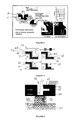
Figure 4 is a schematic cross-sectional diagram of four stages of the fabrication of an L-shaped spacer used within the HBT offigure 3 ; -
Figure 5 is a scanning electron micrograph of an HBT fabricated using L-shaped spacers; -
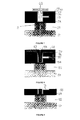
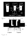
Figures 6 to 11 are schematic cross-sectional diagrams of a portion of an HBT fabricated with r-shaped (gamma-shaped) spacers (on the right hand side of the drawings) showing various stages in the fabrication sequence and compared with a corresponding L-shaped spacer (on the left hand side of the drawings); -
Figures 12 and 13 are schematic cross-sectional diagrams of a portion of an HBT fabricated with r-shaped spacers using a different process than shown infigures 6 to 11 ; -
Figure 14 is a cross-sectional schematic diagram illustrating properties of an HBT affected by L-shaped spacers; -
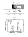
Figure 15 is a graph showing a comparison of the total base resistance for L-shaped and r-shaped spacers; -
Figure 16 is a schematic cross-sectional diagram of a portion of a generally oblique-shaped spacer; -
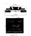
Figure 17 is a scanning electron micrograph of a gamma-shaped spacer formed using the processes described above; and -
Figure 18 is a schematic cross-sectional diagram and corresponding pair of scanning electron micrographs of L-shaped and gamma-shaped spacers. - The inventors have recognised that it would be advantageous to provide a spacer which separates parts of the base and emitter of the transistor in which the spacer is at least as wide at the top of the spacer as it is at the base of the spacer. More preferably, it would be advantageous to provide such a spacer which is wider at the top of the spacer than it is at the bottom of the spacer. A number of process techniques for the formation of such a spacer are now described.
- Throughout this specification, including the description, drawings, claims and abstract, the expressions "collector", "base" and "emitter" (or "collector region", "base region" and "emitter region") are used for convenience to respectively define (i) a first region in the semiconductor substrate that provides a first dopant level and dopant type, (ii) a second region of semiconductor disposed on the substrate and having a second dopant level and second dopant type to form a junction with the first region, and (iii) a third region of semiconductor disposed on the second region and having a third dopant level and third dopant type. The first and third dopant types could be the same. The first, second and third dopant types could be n, p, n respectively, or p, n, p respectively. It will be understood that the devices described here could be inverted so that an emitter region is formed in the substrate and a collector region formed over the substrate. The labels are to be construed accordingly.
- A first process for creating a r-shaped (gamma-shaped) spacer is described with reference to
figures 6 to 11 . The process is shown with schematic cross-sections. In each of the figures an L-shaped spacer process as discussed in connection withfigure 4 is illustrated on the left hand side of the respective figure and the modified process for producing a gamma-shaped spacer is illustrated on the right hand side of the figure, for easy comparison. - Within
substrate 51 is formed acollector region 52 and shallowtrench isolation regions 53 in conventional manner. Apolysilicon gate layer 54 is deposited onto the substrate, followed by a silicon nitride planarization (CMP stopping)layer 55 and apolysilicon cap layer 56. A photolithography stage follows to define a base window opening in photoresist (not shown) over thepolysilicon cap layer 56. Thebase window 60 is then formed by etching through thepolysilicon cap layer 56, thenitride layer 55 and thepolysilicon gate layer 54. This is preferably performed using a single anisotropic etch, e.g. dry etch process. This dry etch is followed by a separate lateral etch of thenitride layer 55 to undercut the polysilicon cap layer to provide a somewhat re-entrant or recessed profile of the walls of thebase window 60, as shown infigure 6 . This nitride etch is preferably a wet etch process, e.g. using H3PO4. Note that therecess 61 in thenitride layer 55 is shown greatly exaggerated for clarity, as will become apparent later. Note also that thepolysilicon cap layer 56 does not form part of an L-shaped spacer production process on the left hand side of the figure. The photoresist layer may be removed after the first (dry) etch process, or after the second (wet) etch process. Other etch strategies may be possible to obtain the required profile of base window, for example by a separate first etch through thepolysilicon cap layer 56 followed by a second etch through thenitride layer 55 and a third etch through thepolysilicon gate layer 54. - A
base stack 57 andepitaxial base layer 58 of Si/SiGe:C/Si is then formed over the etched base window profile resulting in the structure shown infigure 6 . - Turning now to
figure 7 , aspacer 63 is formed by deposition of a suitable spacer material which fills thebase window 60 and is then etched back using a process similar to that shown infigure 2 . In one arrangement, similar tofigure 2 , the spacer formation process first forms a first thin layer ofsilicon oxide 41, followed by a layer ofsilicon nitride 42, followed by a second thin layer ofsilicon oxide 43 followed by a polysilicon spacer material which is then processed similar to that described forfigure 2 . In a preferred process as shown infigure 7 , the spacer formation process first forms a first thin layer ofsilicon oxide 41, followed by a layer ofsilicon nitride 42, followed by a second much thicker layer ofsilicon oxide 43. A dielectric layer is preferred for the spacers, e.g. silicon oxide or silicon nitride. The layer of silicon oxide could be formed using a known TEOS deposition process. An anisotropic etch of thesecond oxide layer 43 to an endpoint of exposure of thenitride layer 42 leaves a wedge-shapedoxide spacer 63 as shown infigure 7 . - The spacer could be formed using various processes, including use of only oxide layers, using the oxide and nitride layers as shown, or using a polysilicon-based spacer as shown in
figure 2 . The use of an oxide-nitride-oxide sandwich is preferred as it allows for triggering an etch endpoint on exposure of the nitride layer. More generally, the spacer may be formed from any suitable electrically insulating material such as a dielectric material or combination of insulating layers which facilitate generally conformal coverage of the recessed or stepped base window profile and a subsequent etch that stops on theepitaxial base layer 58 in theemitter window 9 while leaving some coverage on the sidewalls of the base stack. - The width of the lower part of the spacer is a function of the deposited thickness of the oxide (or other spacer material), the height of the step (sum of deposited
polysilicon gate layer 54 + silicon nitrideCMP stopping layer 55 + polysilicon cap layer 56) and the total etch time. - Following the oxide spacer etch, the uncovered
thin nitride layer 42 is removed using a suitable wet etch, with the remainingsecond oxide layer 43 acting as a hard mask. The remaining exposed firstthin oxide layer 41 on thebase stack layer 57 andepitaxial base layer 58 is removed and then apolysilicon emitter layer 59 is deposited, resulting in the structure shown infigure 8 . - A planarization process follows that aims to stop halfway through the
nitride planarization layer 55, as shown infigure 9 . In the planarization process, all layers are removed in a planar fashion, e.g. using a chemical and/or mechanical removal process as known in the art, down to a level part way through theplanarization layer 55. Thenitride planarization layer 55 thickness (tnit) can be tuned to meet the planarization within-wafer-uniformity requirements: athicker nitride layer 55 creates a larger thickness of oxide (tox) in the recessedportion 61 of the spacer, as shown infigure 8 . The thicker thenitride planarization layer 55, the greater is the process window available for the planarization. A typical value for the within-wafer-uniformity is 30-50 nm. Preferably, the planarization process stops approximately at a midpoint of the planarization layer. More preferably, the planarization process stops approximately at the widest part of thespacer 63. The resulting structure is shown infigure 9 where a r-shaped spacer can clearly be seen. - After planarization, the remaining nitride planarization
CMP stopping layer 55 is removed, e.g. with a wet etch of phosphoric acid, H3PO4. The resulting cross-section is shown inFigure 10 . As mentioned earlier, the diagrams have been shown exaggerated so that thetop portion 70 of the resulting gamma-shapedspacer 71 is much wider than in reality. A more proportionately drawn gamma-shapedspacer 71 is shown infigure 11 , compared with an L-shapedspacer 20.Figure 11 also shows asubsequent silicide layer 72 formed on the top of thepolysilicon emitter layer 59 and the epitaxialbase stack layer 57. The larger width of the top 70 of the gamma-shapedspacer 71 offers a substantially improved process margin to avoidsilicide 72 bridging than does the L-shapedspacer 20, and also considerably reduces the width of the spacer at the bottom in contact with theepitaxial base layer 58. This results in alarger emitter window 9 width WE, with consequent improvement in base link resistance and base-collector capacitance, as explained earlier. - The thin polycrystalline or amorphous
silicon cap layer 56 that is used to enable a lateral etch of thesilicon nitride layer 55 and thereby form a recess as shown infigure 6 can have a further benefit in reducing defect formation during epitaxial deposition of theepitaxial base layer 58 andbase stack 57. - The width of the
spacer 71 at the top may be considered as the width of the spacer after planarization, i.e. the width of the top of the spacer as shown infigure 9 and therefore the width of the spacer in the plane on which the silicidation process is subsequently carried out. The width of the spacer at the bottom may be considered as the width of the spacer where it abuts theepitaxial base layer 58, i.e. the portion adjacent to the plane of the emitter / base interface or emitter window. - This process is similar to
process 1 described above, but does not require a thin polycrystalline or amorphoussilicon cap layer 56 on top of thesilicon nitride layer 55. - In this process, after the formation of the
base window 60 by etching through thenitride layer 55 and thepolysilicon gate layer 54 and removal of any photolithography resist, thenitride layer 55 is etched briefly using an isotropic (e.g. wet) etch to cause lateral etching of the nitride window so that the nitride window is effectively larger than the underlying polysilicon gate layer window, as evident infigure 12 . It will be understood that this isotropic nitride etch will also slightly reduce the thickness of the nitride layer as shown since the top is not protected by a polysilicon cap layer. However, this can be factored into the thickness ofnitride layer 55 initially deposited. -
Figure 12 shows the structure after deposition of the firstthin oxide layer 41, thethin nitride layer 42 and theoxide spacer layer 43 and after the anisotropic etch of theoxide spacer layer 43 to leave theoxide spacer 63. This is analogous tofigure 7 . However, in this case, the spacer does not fill arecess 61 as shown infigure 7 , but rather occupies aledge 62 near the height of the base of thenitride layer 55. - Following planarization down to approximately mid-way through the
nitride layer 55, the structure is as shown infigure 13 , analogous tofigure 9 . In similar manner to that shown and described with reference tofigures 10 and11 , the remainder of thenitride planarization layer 55 is removed. The spacer width is still determined by the oxide spacer etch, and the extra margin created at the top by theledge 62 again does not increase the width of thespacer 61 at the bottom. - Similar to that described for
process 1, the width of the spacer at the top may be considered as the width of the spacer after planarization, i.e. the width of the top of the spacer as shown infigure 13 and therefore the width in the plane on which the silicidation process is subsequently carried out. The width of the spacer at the bottom may be considered as the width of the spacer where it abuts theepitaxial base layer 58. - Using the gamma-shaped
spacers 71 described herein leads to a lower total base resistance by means of a reduction of the base link resistance part.Figure 14 shows a schematic diagram of the emitter-base region indicating the extrinsic region base resistance (RXB), the link region base resistance (Rlink) and the intrinsic region base resistance (Rint) part of the base resistance for an L-shaped spacer. - The total base resistance can be written (for standard double base contact devices) as RB = RXB + Rlink + Rint with


W spacer L-spacer gamma-shaped spacer (∼150 nm) (∼50 nm) R int 5.2 Ω 5.2 Ω R XB 15 Ω 15 Ω Rlink 9.4 Ω 3.1 Ω -
Figure 15 shows an estimate of the contribution to the total base resistance of the link under the spacer compared for the L-shaped spacer and the r-shaped spacer. - From
figure 15 it is clear that a optimized r-shaped spacer has a clear advantage in terms of the contribution of Rlink to the total base resistance. While for the L-shaped spacer, the link resistance is about 30% of the total base resistance, the contribution for the improved spacer is less than 15%. - The general geometrical properties of r-shaped spacers are shown schematically in
figure 16 , where d1 is the width of the Si/SiGe:C/Si base stack 57; d2 is the spacer width at the top of the spacer after planarization; d3 is the distance between the spacer and the emitter contact 11; d4 is the emitter contact width; d7 is the width of the Si/SiGe:C/Si base stack 57 over thepolysilicon gate layer 4; h is the spacer height; and θ is the angle of the spacer. Depending on the precise nature of the control over the downward and lateral etching of the base window through thenitride layer 55 and thegate layer 54, and the consequent rounding of corners of the layers being etched, the spacer profile may in practice move towards spacers having a generally outwardly sloping or "oblique" profile with a possible degree of outward curvature such that the spacer presents a convex surface to theemitter layer 59 and a concave surface to thegate stack 57. The expression "oblique" profile is intended to encompass a spacer that has a generally uniform width or a width which increases slightly towards the top of the spacer, and where the top surface that has a width substantially the same as, or greater than, the width of the bottom surface, is displaced laterally outwardly from the bottom surface. - An example of such an oblique arrangement of spacer with a slightly outwardly curved profile is shown in a SEM in
figure 17 , before planarization. The intended planarization level is indicated byhorizontal line 80 approximately bisecting thenitride planarization layer 55. As can be seen, the width of the bottom of the spacers is of the order of 90 nm and the width of the spacers at the level of theplanarization line 80 is at least as large as this. Specifically, by comparison with the scale markings of 87 and 83.8 nm at the top of the unplanarized spacers, the spacer width at theplanarization line 80 is approximately 120 nm. The emitter window width is approximately 300 nm. It has been found that a top width of the spacer of at least about 50 nm is desirable to avoid silicide bridging between the emitter and the base. Using spacers of the form offigure 1 , a width of 50 nm at the top of the spacer is typically achieved with a width at the bottom of the spacer of 150 nm. A reduction of spacer width from 150 nm down to 50 nm at the bottom of the spacer reduces total base resistance by about 10 to 15 %. -
Figure 18 shows a comparison of the two methods. On the left hand side, an L-shaped spacer has a bottom width of 150 nm and a top width at the planarization level of halfway through the nitride layer of just slightly more than 50 nm. On the right hand side of the figure, a gamma-shaped or oblique spacer having a top width at the same planarization level of about 60 - 70 nm but a base width of about 60 nm. This is achieved with a lateral nitride layer etch of 80 nm. This also adds approximately 160 nm to the top width of theemitter 8, which improves the process margin for aligning the emitter contact 11. - It can be seen from the foregoing process description that the introduction of a nitride etch (e.g. wet etch) after the base window etch but before the epitaxial growth of the
base layer 58 andbase stack 57 provides a control of creation of a gamma- or oblique-shaped spacer with substantial benefits to control of the emitter window dimensions and avoidance of silicide shorts at the top of the spacers. The overall width of the spacers can be tuned using a wet etch in, e.g. hydrofluoric acid. - The invention is particularly suitable to boost the performance of a low-complexity HBT that can be used in mixed signal applications.
- Other embodiments are intentionally within the scope of the accompanying claims.
Claims (15)
- A method of forming a bipolar transistor, comprising the steps of:forming a collector region (2) in a substrate (1);forming a base (57, 58) including a base stack region (57), and an emitter region (59), over the substrate;laterally separating the base stack region (57) and the emitter region (58) from one another by forming an electrically insulating spacer (71) therebetween,the insulating spacer (71) having a width dimension at its top end at least as large as the width dimension at its bottom end.
- The method of claim 1 in which the step of forming a base of the transistor comprises:forming a first base layer (4, 54) on the substrate (1);forming a planarization layer (55) on the first base layer (54);defining a base window (60) through the planarization layer (55) and the first base layer (54) to expose the collector region (2), including etching the planarization layer (55) to a greater lateral extent than the first base layer (54) on which it is formed;depositing a base epitaxial layer (58) on the exposed collector region and a base stack (57) on sidewalls of the base window (60);the method further including the steps of:forming the spacer (71) by forming an electrically insulating layer (41, 42, 43) in the base window (60) and etching the insulating layer so as to leave a residual portion thereof that covers the portion of the base stack that forms the sidewalls of the base window,wherein the greater lateral extent of the etch of the planarization layer results in a widening of the spacer (71) or a sloping outward of the spacer at least part way up the spacer.
- The method of claim 2 further including the step of forming an emitter region in the base window (60) by depositing a semiconductor material (59) over the first base layer (54) and the spacer (71).
- The method of claim 3 further including the step of planarizing the structure by removing all layers down to a depth part way through the planarization layer (55).
- The method of claim 4 in which the step of planarizing the structure comprises removing all layers down to a depth corresponding to a widest part of the spacer (71).
- The method of claim 4 or claim 5 further including forming a silicide layer (72) on the base stack (57) and the emitter region (59) on either side of the spacer (71), the silicide layer being discontinuous over the top surface of the spacer.
- The method of any of claims 2 to 6 in which the step of forming the base (57, 58) of the transistor further comprises the step of forming a cap layer (56) on the planarization layer (55) and defining the base window (60) through said cap layer as well as said planarization layer and said base silicon layer (54), wherein the etching of the planarization layer is performed to a greater lateral extent than the etching of the cap layer so as to undercut the cap layer and form a recessed portion (61) of the base window sidewall prior to forming the base stack (57) thereon.
- The method of claim 2 in which the step of forming the spacer (71) comprises forming said electrically insulating layer as a three layer structure comprising a first silicon oxide layer (41), a silicon nitride layer (42) and a second silicon oxide layer (43) and wherein the etching of said layers to leave said residual portion comprises etching the second silicon layer to end point on the nitride layer, then removing the exposed nitride layer.
- The method of claim 1 in which the spacer is formed so as to have one of a r-shaped or inverted L-shaped structure, or an oblique shape.
- A bipolar transistor structure having a collector (52) formed in a substrate (1) and a base (57, 58) and an emitter (59) formed over the substrate, the base having a base stack region (57) being laterally separated from the emitter (59) on the substrate (1) by an electrically insulating spacer (71), in which the insulating spacer (71) has a width dimension at its top end at least as large as the width dimension at its bottom end.
- The transistor structure of claim 10 in which the spacer (71) has a width dimension at its top end larger than the width dimension at its bottom end.
- The transistor structure of claim 10 or claim 11 in which the spacer (71) is formed as a r-shaped or inverted L-shaped structure.
- The transistor structure of claim 10 or claim 11 in which the spacer is formed as an oblique spacer in which the spacer has a generally uniform width or a width which increases slightly towards the top of the spacer, and where the top surface that has a width substantially the same as, or greater than, the width of the bottom surface, is displaced laterally outwardly from the bottom surface.
- The transistor structure of claim 13 in which the oblique spacer (71) has a curved profile, such that it presents a convex surface to the emitter (59) and a concave surface to the base stack region (57).
- The transistor structure of claim 10 in which the spacer (71) is formed from a silicon oxide or from a silicon oxide and silicon nitride layered structure.
Priority Applications (3)
| Application Number | Priority Date | Filing Date | Title |
|---|---|---|---|
| EP10250714.2A EP2372754B1 (en) | 2010-04-01 | 2010-04-01 | Spacer formation in the fabrication of planar bipolar transistors |
| US13/076,290 US8704335B2 (en) | 2010-04-01 | 2011-03-30 | Spacer formation in the fabrication of planar bipolar transistors |
| CN201110083001.3A CN102214572B (en) | 2010-04-01 | 2011-03-31 | Spacer formation in the fabrication of planar bipolar transistors |
Applications Claiming Priority (1)
| Application Number | Priority Date | Filing Date | Title |
|---|---|---|---|
| EP10250714.2A EP2372754B1 (en) | 2010-04-01 | 2010-04-01 | Spacer formation in the fabrication of planar bipolar transistors |
Publications (2)
| Publication Number | Publication Date |
|---|---|
| EP2372754A1 true EP2372754A1 (en) | 2011-10-05 |
| EP2372754B1 EP2372754B1 (en) | 2018-03-14 |
Family
ID=42358085
Family Applications (1)
| Application Number | Title | Priority Date | Filing Date |
|---|---|---|---|
| EP10250714.2A Active EP2372754B1 (en) | 2010-04-01 | 2010-04-01 | Spacer formation in the fabrication of planar bipolar transistors |
Country Status (3)
| Country | Link |
|---|---|
| US (1) | US8704335B2 (en) |
| EP (1) | EP2372754B1 (en) |
| CN (1) | CN102214572B (en) |
Cited By (2)
| Publication number | Priority date | Publication date | Assignee | Title |
|---|---|---|---|---|
| US9018681B2 (en) | 2010-11-26 | 2015-04-28 | Nxp B.V. | Method of manufacturing a bipolar transistor and bipolar transistor |
| CN115985774A (en) * | 2023-02-21 | 2023-04-18 | 上海华虹宏力半导体制造有限公司 | Bipolar transistor device and method of making the same |
Families Citing this family (5)
| Publication number | Priority date | Publication date | Assignee | Title |
|---|---|---|---|---|
| EP2418681B1 (en) | 2010-08-10 | 2017-10-11 | Nxp B.V. | Heterojunction Bipolar Transistor and Manufacturing Method |
| EP2458624A1 (en) | 2010-11-26 | 2012-05-30 | Nxp B.V. | Heterojunction Bipolar Transistor Manufacturing Method and Integrated Circuit Comprising a Heterojunction Bipolar Transistor |
| EP2747131B1 (en) | 2012-12-18 | 2015-07-01 | Nxp B.V. | Method of processing a silicon wafer |
| US9722057B2 (en) * | 2015-06-23 | 2017-08-01 | Global Foundries Inc. | Bipolar junction transistors with a buried dielectric region in the active device region |
| US20230178638A1 (en) * | 2021-12-06 | 2023-06-08 | Globalfoundries Singapore Pte. Ltd. | Bipolar transistors |
Citations (5)
| Publication number | Priority date | Publication date | Assignee | Title |
|---|---|---|---|---|
| EP0418185A1 (en) * | 1989-09-11 | 1991-03-20 | International Business Machines Corporation | Method of fabricating a narrow base transistor |
| US5235206A (en) * | 1990-10-24 | 1993-08-10 | International Business Machines Corporation | Vertical bipolar transistor with recessed epitaxially grown intrinsic base region |
| US6156595A (en) * | 1997-10-08 | 2000-12-05 | Sawada; Shigeki | Method of fabricating a Bi-CMOS IC device including a self-alignment bipolar transistor capable of high speed operation |
| EP1134797A2 (en) * | 2000-03-14 | 2001-09-19 | Nec Corporation | Bipolar transistor having recessed and rounded surface and its manufacturing method |
| US7687887B1 (en) * | 2006-12-01 | 2010-03-30 | National Semiconductor Corporation | Method of forming a self-aligned bipolar transistor structure using a selectively grown emitter |
Family Cites Families (8)
| Publication number | Priority date | Publication date | Assignee | Title |
|---|---|---|---|---|
| US5227316A (en) * | 1985-01-22 | 1993-07-13 | National Semiconductor Corporation | Method of forming self aligned extended base contact for a bipolar transistor having reduced cell size |
| JP2611640B2 (en) * | 1993-12-20 | 1997-05-21 | 日本電気株式会社 | Heterojunction bipolar transistor |
| US5866462A (en) * | 1995-09-29 | 1999-02-02 | Analog Devices, Incorporated | Double-spacer technique for forming a bipolar transistor with a very narrow emitter |
| US6239477B1 (en) * | 1998-10-07 | 2001-05-29 | Texas Instruments Incorporated | Self-aligned transistor contact for epitaxial layers |
| JP2005527979A (en) * | 2002-05-29 | 2005-09-15 | コーニンクレッカ フィリップス エレクトロニクス エヌ ヴィ | Method of manufacturing SiGe heterojunction bipolar transistor |
| US7022578B2 (en) | 2003-10-09 | 2006-04-04 | Chartered Semiconductor Manufacturing Ltd. | Heterojunction bipolar transistor using reverse emitter window |
| ATE496393T1 (en) * | 2005-11-21 | 2011-02-15 | Nxp Bv | METHOD FOR PRODUCING A SEMICONDUCTOR COMPONENT AND SEMICONDUCTOR COMPONENT OBTAINED BY SUCH A METHOD |
| US8405127B2 (en) * | 2008-02-20 | 2013-03-26 | International Business Machines Corporation | Method and apparatus for fabricating a heterojunction bipolar transistor |
-
2010
- 2010-04-01 EP EP10250714.2A patent/EP2372754B1/en active Active
-
2011
- 2011-03-30 US US13/076,290 patent/US8704335B2/en active Active
- 2011-03-31 CN CN201110083001.3A patent/CN102214572B/en active Active
Patent Citations (5)
| Publication number | Priority date | Publication date | Assignee | Title |
|---|---|---|---|---|
| EP0418185A1 (en) * | 1989-09-11 | 1991-03-20 | International Business Machines Corporation | Method of fabricating a narrow base transistor |
| US5235206A (en) * | 1990-10-24 | 1993-08-10 | International Business Machines Corporation | Vertical bipolar transistor with recessed epitaxially grown intrinsic base region |
| US6156595A (en) * | 1997-10-08 | 2000-12-05 | Sawada; Shigeki | Method of fabricating a Bi-CMOS IC device including a self-alignment bipolar transistor capable of high speed operation |
| EP1134797A2 (en) * | 2000-03-14 | 2001-09-19 | Nec Corporation | Bipolar transistor having recessed and rounded surface and its manufacturing method |
| US7687887B1 (en) * | 2006-12-01 | 2010-03-30 | National Semiconductor Corporation | Method of forming a self-aligned bipolar transistor structure using a selectively grown emitter |
Cited By (2)
| Publication number | Priority date | Publication date | Assignee | Title |
|---|---|---|---|---|
| US9018681B2 (en) | 2010-11-26 | 2015-04-28 | Nxp B.V. | Method of manufacturing a bipolar transistor and bipolar transistor |
| CN115985774A (en) * | 2023-02-21 | 2023-04-18 | 上海华虹宏力半导体制造有限公司 | Bipolar transistor device and method of making the same |
Also Published As
| Publication number | Publication date |
|---|---|
| US8704335B2 (en) | 2014-04-22 |
| US20120168908A1 (en) | 2012-07-05 |
| CN102214572B (en) | 2014-11-05 |
| EP2372754B1 (en) | 2018-03-14 |
| CN102214572A (en) | 2011-10-12 |
Similar Documents
| Publication | Publication Date | Title |
|---|---|---|
| EP2372754B1 (en) | Spacer formation in the fabrication of planar bipolar transistors | |
| EP3547371B1 (en) | Bipolar transistor and method of manufacturing a bipolar transistor | |
| US6472262B2 (en) | Method for fabricating a bipolar transistor of the self-aligned double-polysilicon type with a heterojunction base and corresponding transistor | |
| US8872237B2 (en) | Heterojunction bipolar transistor manufacturing method and integrated circuit comprising a heterojunction bipolar transistor | |
| US8101491B2 (en) | Heterojunction bipolar transistor | |
| US8431966B2 (en) | Method of manufacturing a bipolar transistor semiconductor device and semiconductor devices obtained thereby | |
| US20120119262A1 (en) | SiGe Heterojunction Bipolar Transistor and Method of Forming a SiGe Heterojunction Bipolar Transistor | |
| JP3890202B2 (en) | Manufacturing method of semiconductor device | |
| EP0147249B1 (en) | Method of manufacturing transistor structures having junctions bound by insulating layers, and resulting structures | |
| JP2002525874A (en) | Bipolar transistor and method of manufacturing the same | |
| JP2004518284A (en) | Semiconductor tiling structure and method of manufacturing the same | |
| US7192838B2 (en) | Method of producing complementary SiGe bipolar transistors | |
| US10032868B2 (en) | High performance super-beta NPN (SBNPN) | |
| CN117238770B (en) | Trench gate MOSFET device and manufacturing method thereof | |
| US6927118B2 (en) | Method of fabricating a bipolar transistor utilizing a dry etching and a wet etching to define a base junction opening | |
| US6444536B2 (en) | Method for fabricating bipolar transistors | |
| US20090212394A1 (en) | Bipolar transistor and method of fabricating the same | |
| EP2506297A1 (en) | Bi-CMOS Device and Method | |
| US8268688B2 (en) | Production of VDMOS-transistors having optimized gate contact | |
| US20040251515A1 (en) | Bipolar junction transistors and methods of manufacturing the same | |
| US20060011968A1 (en) | Semiconductor devices and methods of forming the same | |
| CN107785412B (en) | Method for manufacturing bipolar junction transistor and bipolar junction transistor | |
| EP1489662A2 (en) | Bipolar junction transistor and method of manufacturing the same | |
| US20040075119A1 (en) | Forming polysilicon structures | |
| HK1104667B (en) | Method of forming a self-aligned transistor and structure therefor |
Legal Events
| Date | Code | Title | Description |
|---|---|---|---|
| PUAI | Public reference made under article 153(3) epc to a published international application that has entered the european phase |
Free format text: ORIGINAL CODE: 0009012 |
|
| AK | Designated contracting states |
Kind code of ref document: A1 Designated state(s): AT BE BG CH CY CZ DE DK EE ES FI FR GB GR HR HU IE IS IT LI LT LU LV MC MK MT NL NO PL PT RO SE SI SK SM TR |
|
| AX | Request for extension of the european patent |
Extension state: AL BA ME RS |
|
| 17P | Request for examination filed |
Effective date: 20120405 |
|
| 17Q | First examination report despatched |
Effective date: 20130709 |
|
| GRAP | Despatch of communication of intention to grant a patent |
Free format text: ORIGINAL CODE: EPIDOSNIGR1 |
|
| STAA | Information on the status of an ep patent application or granted ep patent |
Free format text: STATUS: GRANT OF PATENT IS INTENDED |
|
| INTG | Intention to grant announced |
Effective date: 20170629 |
|
| GRAJ | Information related to disapproval of communication of intention to grant by the applicant or resumption of examination proceedings by the epo deleted |
Free format text: ORIGINAL CODE: EPIDOSDIGR1 |
|
| STAA | Information on the status of an ep patent application or granted ep patent |
Free format text: STATUS: EXAMINATION IS IN PROGRESS |
|
| INTC | Intention to grant announced (deleted) | ||
| GRAP | Despatch of communication of intention to grant a patent |
Free format text: ORIGINAL CODE: EPIDOSNIGR1 |
|
| STAA | Information on the status of an ep patent application or granted ep patent |
Free format text: STATUS: GRANT OF PATENT IS INTENDED |
|
| INTG | Intention to grant announced |
Effective date: 20170929 |
|
| GRAS | Grant fee paid |
Free format text: ORIGINAL CODE: EPIDOSNIGR3 |
|
| GRAA | (expected) grant |
Free format text: ORIGINAL CODE: 0009210 |
|
| STAA | Information on the status of an ep patent application or granted ep patent |
Free format text: STATUS: THE PATENT HAS BEEN GRANTED |
|
| AK | Designated contracting states |
Kind code of ref document: B1 Designated state(s): AT BE BG CH CY CZ DE DK EE ES FI FR GB GR HR HU IE IS IT LI LT LU LV MC MK MT NL NO PL PT RO SE SI SK SM TR |
|
| REG | Reference to a national code |
Ref country code: GB Ref legal event code: FG4D |
|
| REG | Reference to a national code |
Ref country code: CH Ref legal event code: EP Ref country code: AT Ref legal event code: REF Ref document number: 979632 Country of ref document: AT Kind code of ref document: T Effective date: 20180315 |
|
| REG | Reference to a national code |
Ref country code: IE Ref legal event code: FG4D |
|
| REG | Reference to a national code |
Ref country code: DE Ref legal event code: R096 Ref document number: 602010049146 Country of ref document: DE |
|
| REG | Reference to a national code |
Ref country code: FR Ref legal event code: PLFP Year of fee payment: 9 |
|
| REG | Reference to a national code |
Ref country code: NL Ref legal event code: MP Effective date: 20180314 |
|
| REG | Reference to a national code |
Ref country code: LT Ref legal event code: MG4D |
|
| PG25 | Lapsed in a contracting state [announced via postgrant information from national office to epo] |
Ref country code: NO Free format text: LAPSE BECAUSE OF FAILURE TO SUBMIT A TRANSLATION OF THE DESCRIPTION OR TO PAY THE FEE WITHIN THE PRESCRIBED TIME-LIMIT Effective date: 20180614 Ref country code: FI Free format text: LAPSE BECAUSE OF FAILURE TO SUBMIT A TRANSLATION OF THE DESCRIPTION OR TO PAY THE FEE WITHIN THE PRESCRIBED TIME-LIMIT Effective date: 20180314 Ref country code: LT Free format text: LAPSE BECAUSE OF FAILURE TO SUBMIT A TRANSLATION OF THE DESCRIPTION OR TO PAY THE FEE WITHIN THE PRESCRIBED TIME-LIMIT Effective date: 20180314 Ref country code: HR Free format text: LAPSE BECAUSE OF FAILURE TO SUBMIT A TRANSLATION OF THE DESCRIPTION OR TO PAY THE FEE WITHIN THE PRESCRIBED TIME-LIMIT Effective date: 20180314 Ref country code: ES Free format text: LAPSE BECAUSE OF FAILURE TO SUBMIT A TRANSLATION OF THE DESCRIPTION OR TO PAY THE FEE WITHIN THE PRESCRIBED TIME-LIMIT Effective date: 20180314 Ref country code: CY Free format text: LAPSE BECAUSE OF FAILURE TO SUBMIT A TRANSLATION OF THE DESCRIPTION OR TO PAY THE FEE WITHIN THE PRESCRIBED TIME-LIMIT Effective date: 20180314 |
|
| REG | Reference to a national code |
Ref country code: AT Ref legal event code: MK05 Ref document number: 979632 Country of ref document: AT Kind code of ref document: T Effective date: 20180314 |
|
| PG25 | Lapsed in a contracting state [announced via postgrant information from national office to epo] |
Ref country code: SE Free format text: LAPSE BECAUSE OF FAILURE TO SUBMIT A TRANSLATION OF THE DESCRIPTION OR TO PAY THE FEE WITHIN THE PRESCRIBED TIME-LIMIT Effective date: 20180314 Ref country code: LV Free format text: LAPSE BECAUSE OF FAILURE TO SUBMIT A TRANSLATION OF THE DESCRIPTION OR TO PAY THE FEE WITHIN THE PRESCRIBED TIME-LIMIT Effective date: 20180314 Ref country code: GR Free format text: LAPSE BECAUSE OF FAILURE TO SUBMIT A TRANSLATION OF THE DESCRIPTION OR TO PAY THE FEE WITHIN THE PRESCRIBED TIME-LIMIT Effective date: 20180615 Ref country code: BG Free format text: LAPSE BECAUSE OF FAILURE TO SUBMIT A TRANSLATION OF THE DESCRIPTION OR TO PAY THE FEE WITHIN THE PRESCRIBED TIME-LIMIT Effective date: 20180614 |
|
| PG25 | Lapsed in a contracting state [announced via postgrant information from national office to epo] |
Ref country code: PL Free format text: LAPSE BECAUSE OF FAILURE TO SUBMIT A TRANSLATION OF THE DESCRIPTION OR TO PAY THE FEE WITHIN THE PRESCRIBED TIME-LIMIT Effective date: 20180314 Ref country code: EE Free format text: LAPSE BECAUSE OF FAILURE TO SUBMIT A TRANSLATION OF THE DESCRIPTION OR TO PAY THE FEE WITHIN THE PRESCRIBED TIME-LIMIT Effective date: 20180314 Ref country code: IT Free format text: LAPSE BECAUSE OF FAILURE TO SUBMIT A TRANSLATION OF THE DESCRIPTION OR TO PAY THE FEE WITHIN THE PRESCRIBED TIME-LIMIT Effective date: 20180314 Ref country code: RO Free format text: LAPSE BECAUSE OF FAILURE TO SUBMIT A TRANSLATION OF THE DESCRIPTION OR TO PAY THE FEE WITHIN THE PRESCRIBED TIME-LIMIT Effective date: 20180314 Ref country code: NL Free format text: LAPSE BECAUSE OF FAILURE TO SUBMIT A TRANSLATION OF THE DESCRIPTION OR TO PAY THE FEE WITHIN THE PRESCRIBED TIME-LIMIT Effective date: 20180314 |
|
| PG25 | Lapsed in a contracting state [announced via postgrant information from national office to epo] |
Ref country code: CZ Free format text: LAPSE BECAUSE OF FAILURE TO SUBMIT A TRANSLATION OF THE DESCRIPTION OR TO PAY THE FEE WITHIN THE PRESCRIBED TIME-LIMIT Effective date: 20180314 Ref country code: SM Free format text: LAPSE BECAUSE OF FAILURE TO SUBMIT A TRANSLATION OF THE DESCRIPTION OR TO PAY THE FEE WITHIN THE PRESCRIBED TIME-LIMIT Effective date: 20180314 Ref country code: AT Free format text: LAPSE BECAUSE OF FAILURE TO SUBMIT A TRANSLATION OF THE DESCRIPTION OR TO PAY THE FEE WITHIN THE PRESCRIBED TIME-LIMIT Effective date: 20180314 Ref country code: SK Free format text: LAPSE BECAUSE OF FAILURE TO SUBMIT A TRANSLATION OF THE DESCRIPTION OR TO PAY THE FEE WITHIN THE PRESCRIBED TIME-LIMIT Effective date: 20180314 |
|
| REG | Reference to a national code |
Ref country code: CH Ref legal event code: PL |
|
| REG | Reference to a national code |
Ref country code: DE Ref legal event code: R097 Ref document number: 602010049146 Country of ref document: DE |
|
| REG | Reference to a national code |
Ref country code: BE Ref legal event code: MM Effective date: 20180430 |
|
| PG25 | Lapsed in a contracting state [announced via postgrant information from national office to epo] |
Ref country code: PT Free format text: LAPSE BECAUSE OF FAILURE TO SUBMIT A TRANSLATION OF THE DESCRIPTION OR TO PAY THE FEE WITHIN THE PRESCRIBED TIME-LIMIT Effective date: 20180716 |
|
| PLBE | No opposition filed within time limit |
Free format text: ORIGINAL CODE: 0009261 |
|
| STAA | Information on the status of an ep patent application or granted ep patent |
Free format text: STATUS: NO OPPOSITION FILED WITHIN TIME LIMIT |
|
| REG | Reference to a national code |
Ref country code: IE Ref legal event code: MM4A |
|
| PG25 | Lapsed in a contracting state [announced via postgrant information from national office to epo] |
Ref country code: DK Free format text: LAPSE BECAUSE OF FAILURE TO SUBMIT A TRANSLATION OF THE DESCRIPTION OR TO PAY THE FEE WITHIN THE PRESCRIBED TIME-LIMIT Effective date: 20180314 Ref country code: LU Free format text: LAPSE BECAUSE OF NON-PAYMENT OF DUE FEES Effective date: 20180401 Ref country code: MC Free format text: LAPSE BECAUSE OF FAILURE TO SUBMIT A TRANSLATION OF THE DESCRIPTION OR TO PAY THE FEE WITHIN THE PRESCRIBED TIME-LIMIT Effective date: 20180314 |
|
| 26N | No opposition filed |
Effective date: 20181217 |
|
| GBPC | Gb: european patent ceased through non-payment of renewal fee |
Effective date: 20180614 |
|
| PG25 | Lapsed in a contracting state [announced via postgrant information from national office to epo] |
Ref country code: CH Free format text: LAPSE BECAUSE OF NON-PAYMENT OF DUE FEES Effective date: 20180430 Ref country code: LI Free format text: LAPSE BECAUSE OF NON-PAYMENT OF DUE FEES Effective date: 20180430 Ref country code: BE Free format text: LAPSE BECAUSE OF NON-PAYMENT OF DUE FEES Effective date: 20180430 Ref country code: SI Free format text: LAPSE BECAUSE OF FAILURE TO SUBMIT A TRANSLATION OF THE DESCRIPTION OR TO PAY THE FEE WITHIN THE PRESCRIBED TIME-LIMIT Effective date: 20180314 |
|
| PG25 | Lapsed in a contracting state [announced via postgrant information from national office to epo] |
Ref country code: GB Free format text: LAPSE BECAUSE OF NON-PAYMENT OF DUE FEES Effective date: 20180614 Ref country code: IE Free format text: LAPSE BECAUSE OF NON-PAYMENT OF DUE FEES Effective date: 20180401 |
|
| PG25 | Lapsed in a contracting state [announced via postgrant information from national office to epo] |
Ref country code: MT Free format text: LAPSE BECAUSE OF NON-PAYMENT OF DUE FEES Effective date: 20180401 |
|
| PG25 | Lapsed in a contracting state [announced via postgrant information from national office to epo] |
Ref country code: TR Free format text: LAPSE BECAUSE OF FAILURE TO SUBMIT A TRANSLATION OF THE DESCRIPTION OR TO PAY THE FEE WITHIN THE PRESCRIBED TIME-LIMIT Effective date: 20180314 |
|
| PG25 | Lapsed in a contracting state [announced via postgrant information from national office to epo] |
Ref country code: HU Free format text: LAPSE BECAUSE OF FAILURE TO SUBMIT A TRANSLATION OF THE DESCRIPTION OR TO PAY THE FEE WITHIN THE PRESCRIBED TIME-LIMIT; INVALID AB INITIO Effective date: 20100401 |
|
| PG25 | Lapsed in a contracting state [announced via postgrant information from national office to epo] |
Ref country code: MK Free format text: LAPSE BECAUSE OF NON-PAYMENT OF DUE FEES Effective date: 20180314 |
|
| PG25 | Lapsed in a contracting state [announced via postgrant information from national office to epo] |
Ref country code: IS Free format text: LAPSE BECAUSE OF FAILURE TO SUBMIT A TRANSLATION OF THE DESCRIPTION OR TO PAY THE FEE WITHIN THE PRESCRIBED TIME-LIMIT Effective date: 20180714 |
|
| P01 | Opt-out of the competence of the unified patent court (upc) registered |
Effective date: 20230724 |
|
| REG | Reference to a national code |
Ref country code: DE Ref legal event code: R079 Ref document number: 602010049146 Country of ref document: DE Free format text: PREVIOUS MAIN CLASS: H01L0021331000 Ipc: H10D0012010000 |
|
| PGFP | Annual fee paid to national office [announced via postgrant information from national office to epo] |
Ref country code: DE Payment date: 20250319 Year of fee payment: 16 |
|
| PGFP | Annual fee paid to national office [announced via postgrant information from national office to epo] |
Ref country code: FR Payment date: 20260319 Year of fee payment: 17 |